DS405-00008-1v0-E - Fujitsu Global MB39C601 PIN ASSIGNMENT (TOP VIEW) 4 3 2 1 OTM PCL TZE FB VDD VCG...
32
Copyright©2012 FUJITSU SEMICONDUCTOR LIMITED All rights reserved 2012.12 FUJITSU SEMICONDUCTOR DATA SHEET DS405-00008-1v0-E Power Supply online Design Simulation Easy DesignSim This product supports the web-based design simulation tool. It can easily select external components and can display useful information. Please access from the following URL. http://edevice.fujitsu.com/pmic/en-easy/?m=ds ASSP TRIAC Dimmable LED Driver IC for LED Lighting MB39C601 DESCRIPTION MB39C601 is a flyback type switching regulator contorller IC. The LED current is regulated by controlling the switching on-time or controlling the switching frequency, depending on the LED load. It is most suitable for the general lighting applications, for example stocks of commercial and residential light bulbs and so on. FEATURES High power factor in single conversion High efficiency at the light load, at Low Power Mode (LPM) Burst Operation in switching frequency control Frequency setting depend on the FB pin current : 30 kHz to 130 kHz Control of the current of Primary Winding without the external sense resistor TRIAC Dimmable LED lighting Helps to achieve high efficiency and low EMI by detecting transformer zero energy Built-in under voltage lock out function Built-in over load protection function Built-in output over voltage protection function Built-in over temperature protection function LED load :25W (Max) Input voltage range VDD : 9V to 20V Input voltage range for LED lighting applications : AC110V RMS , AC230V RMS Package : SOP-8 (3.9mm × 5.05mm × 1.75mm [Max]) APPLICATIONS LED lighting TRIAC dimmable LED lighting etc.
Transcript of DS405-00008-1v0-E - Fujitsu Global MB39C601 PIN ASSIGNMENT (TOP VIEW) 4 3 2 1 OTM PCL TZE FB VDD VCG...

Copyright©2012 FUJITSU SEMICONDUCTOR LIMITED All rights reserved 2012.12
FUJITSU SEMICONDUCTOR DATA SHEET DS405-00008-1v0-E
FUJITSU SEMICONDUCTOR CONFIDENTIAL
Power Supply online Design Simulation Easy DesignSim
This product supports the web-based design simulation tool. It can easily select external components and can display useful information. Please access from the following URL.
http://edevice.fujitsu.com/pmic/en-easy/?m=ds
ASSP
TRIAC Dimmable LED Driver IC for LED Lighting
MB39C601
DESCRIPTION MB39C601 is a flyback type switching regulator contorller IC. The LED current is regulated by controlling the switching on-time or controlling the switching frequency, depending on the LED load. It is most suitable for the general lighting applications, for example stocks of commercial and residential light bulbs and so on.
FEATURES High power factor in single conversion High efficiency at the light load, at Low Power Mode (LPM) Burst Operation in switching frequency
control Frequency setting depend on the FB pin current : 30 kHz to 130 kHz Control of the current of Primary Winding without the external sense resistor TRIAC Dimmable LED lighting Helps to achieve high efficiency and low EMI by detecting transformer zero energy Built-in under voltage lock out function Built-in over load protection function Built-in output over voltage protection function Built-in over temperature protection function LED load :25W (Max) Input voltage range VDD : 9V to 20V Input voltage range for LED lighting applications : AC110VRMS, AC230VRMS Package : SOP-8 (3.9mm × 5.05mm × 1.75mm [Max])
APPLICATIONS LED lighting TRIAC dimmable LED lighting etc.

2
Limitation : development tool vendor use only FUJITSU SEMICONDUCTOR CONFIDENTIAL
DS405-00008-1v0-E
MB39C601
PIN ASSIGNMENT
(TOP VIEW)
4
3
2
1
OTM
PCL
TZE
VDDFB
VCG
GND
DRN
5
6
7
8
(FPT-8P-M02)
PIN DESCRIPTIONS Pin No. Pin Name I/O Description
1 FB I Switching frequency setting pin.
2 TZE I Transformer auxiliary winding zero energy detecting pin.
3 PCL I Pin for controlling peak current of transformer primary winding.
4 OTM I On-time setting pin.
5 VCG - External MOSFET gate bias pin.
6 DRN O External MOSFET source connection pin.
7 GND - Ground pin.
8 VDD - Power supply pin.

3
Limitation : development tool vendor use only FUJITSU SEMICONDUCTOR CONFIDENTIAL
DS405-00008-1v0-E
MB39C601
BLOCK DIAGRAM (On-time control application)
Rst
CV
DD
CB
UL
K
VIN
AC
CV
CG
D1
DB
IAS
Rs
Vs
Co
1
1
1 1
1
11
1
1
1
2
22
210
V/6
V
10V
/8V
VD
D8
FB
1
I FB
Fau
lt La
tch
Res
et
VV
DD
Sw
itch
13V
VV
CG
LDO
VV
CG
Shu
nt
Ena
ble
PW
M
14V
2V
HS
Driv
e
Driv
er
1/t S
W
I FB
Fre
q. M
odul
ator
I FB
VG
AT
E
Dis
char
ge
DQ Q
Ena
ble
PW
M
UV
LO
DR
N6
VC
G5
GN
D7
1.5μ
A<
IFB<
210µ
A
210µ
A<
I FB
I FB<
1.5µ
A
Mod
ulat
ors
Low
Pow
er M
ode
Ove
r Lo
ad
I FB
Fee
dbac
kP
roce
ssin
g
5V
TZ
E2
OV
Fau
lt
On-
Tim
e M
odul
atio
nan
d F
ault
Res
pons
eC
ontr
olF
ault
Tim
ing
and
Con
trol
Fau
lt
Latc
h or
Ret
ry
VG
AT
E
OT
M4
3VI O
TM
1VS
hutd
own
and
Res
tart
The
rmal
Shu
tdow
n
UV
LO
Fau
lt La
tch
Res
et
I P
IFB
PC
L3
Cur
rent
Mod
ulat
orI F
B
MB
39C
601
Cur
rent
Sen
se
20m
V
Zer
o E
nerg
yD
etec
t

4
Limitation : development tool vendor use only FUJITSU SEMICONDUCTOR CONFIDENTIAL
DS405-00008-1v0-E
MB39C601
ABSOLUTE MAXIMUM RATINGS Rating
Parameter Symbol Condition Min Max
Unit
Power supply voltage VVDD VDD pin -0.3 +25.0 V
VDRN DRN pin - +20.0 V
VVCG VCG pin -0.3 +16.0 V
VTZE TZE pin -0.3 +6.0 V
VOTM OTM pin -0.3 +6.0 V
VPCL PCL pin -0.3 +6.0 V
Input voltage
VFB FB pin -0.3 +2.0 V
IVCG VCG pin - 10 mA
IOTM OTM pin -1 0 mA
IPCL PCL pin -1 0 mA Input current
IFB FB pin 0 1 mA
IDRN DRN pin - 800 mA Output current
IDRN DRN pin Pulsed 400ns, 2% duty cycle
-1.5 +6.0 A
Power dissipation PD Ta ≤ +25°C - 800* mW
Storage temperature TSTG -55 +125 °C
*: The value when using two layers PCB. Reference: θja (wind speed 0m/s): 125°C/W
WARNING: Semiconductor devices can be permanently damaged by application of stress (voltage, current, temperature, etc.) in excess of absolute maximum ratings. Do not exceed these ratings.
5
Limitation : development tool vendor use only FUJITSU SEMICONDUCTOR CONFIDENTIAL
DS405-00008-1v0-E
MB39C601
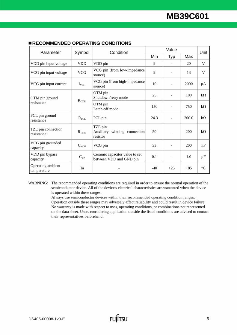
RECOMMENDED OPERATING CONDITIONS Value
Parameter Symbol Condition Min Typ Max
Unit
VDD pin input voltage VDD VDD pin 9 - 20 V
VCG pin input voltage VCG VCG pin (from low-impedance source)
9 - 13 V
VCG pin input current IVCG VCG pin (from high-impedance source)
10 - 2000 µA
OTM pin Shutdown/retry mode
25 - 100 kΩOTM pin ground resistance
ROTM OTM pin Latch-off mode
150 - 750 kΩ
PCL pin ground resistance
RPCL PCL pin 24.3 - 200.0 kΩ
TZE pin connection resistance
RTZE1
TZE pin Auxiliary winding connection resistor
50 - 200 kΩ
VCG pin grounded capacity
CVCG VCG pin 33 - 200 nF
VDD pin bypass capacity
CBP Ceramic capacitor value to set between VDD and GND pin
0.1 - 1.0 µF
Operating ambient temperature
Ta - -40 +25 +85 °C
WARNING: The recommended operating conditions are required in order to ensure the normal operation of the semiconductor device. All of the device's electrical characteristics are warranted when the device is operated within these ranges. Always use semiconductor devices within their recommended operating condition ranges. Operation outside these ranges may adversely affect reliability and could result in device failure. No warranty is made with respect to uses, operating conditions, or combinations not represented on the data sheet. Users considering application outside the listed conditions are advised to contact their representatives beforehand.

6
Limitation : development tool vendor use only FUJITSU SEMICONDUCTOR CONFIDENTIAL
DS405-00008-1v0-E
MB39C601
ELECTRICAL CHARACTERISTICS (Ta = +25°C, VVDD = 12V)
Value Parameter Symbol
Pin No.
Condition Min Typ Max
Unit
VCG voltage (Operating)
VCG
(OPERATING)5 VVDD=14V, IVCG=2.0mA 13 14 15 V
VCG voltage (Disable)
VCG
(DISABLED) 5
VVDD=12V, IVCG=26µA, IFB=350µA
15 16 17 V
VCG voltage difference
ΔVCG 5 VCG(DISABLED)- VCG(OPERATING)
1.75 2.00 2.15 V
VCG Shunt input current
IVCG(SREG) 5 VVCG=VCG(DISABLED)- 100mV, VVDD=12V
- 12 26 µA
VCG Shunt Load Regulation
ΔVCG(SREG) 5 26µA<IVCG ≤ 5mA, IFB=350µA
- 125 200 mV
VCG LDO regulation voltage
VCG(LREG) 5 VVDD=20V, IVCG=-2mA - 13 - V
VCG LDO Dropout voltage
VCG
(LREG, DO) -
VDD-VCG, VVDD=11V, IVCG=-2mA
- 2.0 2.8 V
UVLO Turn-on threshold voltage
VDD(ON) 8 - 9.7 10.2 10.7 V
UVLO Turn-off threshold voltage
VDD(OFF) 8 - 7.55 8.00 8.50 V
UVLO hysteresis ΔVDD(UVLO) 8 VDD(ON) - VDD(OFF) 1.9 2.2 2.5 V
VDD switch on-resistance
RDS, ON (VDD) 6,8VVCG=12V, VVDD=7V, IDRN=50mA
- 4* 10* Ω
VDD and VCG SUPPLY
Fault Latch Reset VDD voltage
VDD
(FAULT RESET)8 - 5.6 6.0 6.4 V

7
Limitation : development tool vendor use only FUJITSU SEMICONDUCTOR CONFIDENTIAL
DS405-00008-1v0-E
MB39C601
Value Parameter Symbol
Pin No.
Condition Min Typ Max
Unit
Minimum switching period
tSW(HF) 6 FM mode IFB=5µA 7.215 7.760 8.305 µs
Maximum switching period
tSW(LF) 6 IFB=IFB, CNR3 -20µA 31.5 35.0 38.5 µs
6 IFB=5µA, IPCL=100μA - 3* - ADRN peak current
IDRN(peak) 6 IFB=5µA, IPCL=30μA - 1* - A
Minimum peak current for RPCL open
IDRN (peak, absmin) 6 RPCL =OPEN - 0.45* - A
ILIM blanking time
tBLANK (ILIM) 6 IFB=5µA, RPCL=100kΩ, 1.2A pull-up on DRN
- 400* - ns
3 IFB=5µA 2.94 3.00 3.06 VPCL voltage VPCL
3 IFB=230µA 0.95 1.00 1.05 V
IFB range for FM mode
IFB, CNR1 1 tS=tS(LF), IDRN=IDRN(peak, max) 145 165 195 µA
IFB range for AM mode
IFB,CNR2- IFB,CNR1
1 tS=tS(LF) , IDRN(peak) variation range= IDRN(peak, max) to IDRN(peak, min)
35 45 65 µA
IFB range for LPM
IFB,CNR3- IFB,CNR2
1 - 50 70 90 µA
IFB hysteresis for LPM
IFB, LPM-HYST 1 - 10 25 40 µA
MODULATION
FB voltage VFB 1 IFB=10µA 0.34 0.70 0.84 V
Driver on-resistance
RDS(on)(DRN) 6,7 IDRN=4.0A - 200* 400* mΩ
Driver off leakage current
IDRN(OFF) 6,7 VDRN=12V - 1.5 20.0 µA
High-side driver on-resistance
RDS(on)(HS-DRV) 5,6High-side Driver current=50mA
- 6* 11* Ω
DRIVER
DRN discharge current
IDIS 6,7VDD=OPEN, DRN=12V, Fault latch set
2.38 3.40 4.42 mA
TZE zero energy threshold voltage
VTZE(TH) 2 - 5* 20* 50* mV
TZE clamp voltage
VTZE(CLAMP) 2 ITZE= -10µA -200 -160 -100 mV
Start timer operation threshold voltage
VTZE(START) 2 - 0.10 0.15 0.20 V
Driver turn-on Delay time
tDRY(TZE) 6 150Ω pull-up 12V on DRN - 150 - ns
Wait time for zero energy detection
tWAIT(TZE) 6 - 2.0 2.4 2.8 µs
TRANSFORMER ZERO ENERGY DETECTION
Start timer period tST 6 VTZE=0V 150 240 300 µs

8
Limitation : development tool vendor use only FUJITSU SEMICONDUCTOR CONFIDENTIAL
DS405-00008-1v0-E
MB39C601
Value Parameter Symbol
Pin No.
Condition Min Typ Max
Unit
OVP threshold voltage
VTZE(OVP) 2 - 4.85 5.00 5.15 V
OVP blanking time
tBLANK, OVP 6 - 0.6 1.0 1.7 µs
OVERVOLTAGE FAULT
Input bias current ITZE(bias) 2 VTZE=5V -0.1 0 +0.1 µA
Over Load detection current
IFB(OL) 1 - 0* 1.5* 3.0* µA
Over Load delay time
tOL 6 IFB=0A 200 250 300 ms
Retry time after Over Load
tRETRY 6 ROTM=76kΩ - 750 - ms
OVERLOAD FAULT
Over Load detection boundary resistance
ROTM(TH) 4 - 100 120 150 kΩ
Shutdown Threshold voltage
VOTM(Vth) 4 OTM=
0.7 1.0 1.3 VSHUTDOWN THRESHOLD
Shutdown OTM current
IOTM, PU 4 VOTM = VOTM(vth) -600 -450 -300 µA
6 ROTM=383kΩ 3.74 4.17 4.60 µsON-Time tOTM
6 ROTM=76kΩ 3.4 3.8 4.2 µsMAXIMUM ON TIME
OTM voltage VOTM 4 - 2.7 3.0 3.3 V
Protection temperature
TSD - Tj, temperature rising - +150* - °C
OTP Protection temperature hysteresis
TSD_HYS - Tj, temperature falling, degrees below TSD
- 25* - °C
IVDD
(STATIC) 8 VVDD=20V, VTZE=1V 1.36 1.80 2.34 mA
Power supply current IVDD
(OPERATING)8 VVDD=20V - 3.0* 3.7* mA
Power supply current for LPM
IVDD(LPM) 8 IFB=350µA - 550 900 µA
POWER SUPPLY CURRENT
Power supply current for UVLO
IVDD(UVLO) 8 VVDD= VDD(ON) - 100mV - 285 500 µA
*: Standard design value

9
Limitation : development tool vendor use only FUJITSU SEMICONDUCTOR CONFIDENTIAL
DS405-00008-1v0-E
MB39C601
FUNCTION EXPLANATION (1) LED Current Control Function
MB39C601 is a flyback type switching regulator controller. The LED current is regulated by controlling the switching on-time or controlling the switching frequency depending on the LED load. The LED current is converted into detecting voltage (Vs) by sense resistor (Rs) connected in series with LED. Vs is compared by an external error amplifier (Err AMP).When Vs falls below a reference voltage, Err AMP output rises and the current that flows into the Opto-Coupler is decreased.
The OTM pin current is controlled via the Opto-Coupler in the on-time control block. In on-time control, it controls on-time at OTM pin current. So, on-time increases when the current of the OTM pin decreases. And the average current supplied to LED is regulated, because on-time is regulated at the constant switching frequency.
The FB pin current is controlled via the Opto-Coupler in the switching frequency control block. In switching frequency control, it controls switching frequency at FB pin current. So, switching frequency becomes high when the current of the FB pin decreases. And the average current supplied to LED is regulated, because switching frequency is regulated at the constant on-time.
(2) Cascode Switching The switch in Primary Winding is a cascode connection.The gate of external MOSFET is connected with the VCG pin, and the source is connected with the drain of internal Driver MOSFET. When the swich is on-state, internal Driver MOSFET is turned on, HS Driver MOSFET is turned off, and the source voltage of external MOSFET goes down to GND. For this period the DC bias is supplied to the gate of external MOSFET from the VCG pin. Therefore external MOSFET is turned on.
When the switch is off-state, internal Driver MOSFET is turned off, HS Driver MOSFET is turned on, and the source voltage of external MOSFET goes up to VCG voltage. For this period the DC bias is supplied to the gate of external MOSFET from VCG pin. Therefore external MOSFET is turned off. Moreover, the current flowing into internal Driver MOSFET is equal to the current of Primary Winding. Therefore, the peak current into Primary Winding can be detected without the sense resistor.
(3) Natural PFC (Power Factor Correction) Function In the AC voltage input, when the input current waveform is brought close to the sine-wave, and the phase difference is brought close to Zero, Power Factor is improved. In the flyback method operating in discontinuous conduction mode, when the input capacitance is set small, the input current almost becomes equal with peak current of Primary Winding.
VBULK : Supply voltage of Primary Winding LMP : Inductance of Primary Winding
tON : On-time
In on-time control, if loop response of Error Amp. is set to lower than the AC frequency (below 1/10 of the AC frequency), on-time can be constant. Therefore, input current is proportional to input voltage, so Power Factor is regulated.
ON
MP
BULK
MP
BULKPEAK
t
L
V
L
V I = =ONt( )
)(( )

10
Limitation : development tool vendor use only FUJITSU SEMICONDUCTOR CONFIDENTIAL
DS405-00008-1v0-E
MB39C601
(4) Power-Up Sequencing When the voltage is input to VBULK, the electric charge is charged to capacitance of the VCG pin (CVCG) through starting resistor (Rst). So, the voltage of the VCG pin rises. The voltage of the DRN pin rises by source follower when the voltage of the VCG pin reaches the threshold voltage of the external HVMOSFET. The DRN pin is connected with the VDD pin through the internal VDD Switch, and VDD capacitor (CVDD) is charged from the DRN pin. When the voltage at the VDD pin reaches the threshold voltage of UVLO, the VDD Switch is turned off, and the internal Bias circuit operates, and the switching is started.
After the switching begins, the voltage at the VDD pin is supplied from Auxiliary Winding through the external diode (DBIAS). The voltage of an Auxiliary Winding is decided by rolling number ratio of Auxiliary Winding and Secondary Winding, and the voltage of Secondary Winding. Therefore, the voltage at the VDD pin is not supplied, until the voltage of Auxiliary Winding rises more than the voltage at the VDD pin. In this period, it is necessary to set the capacitor of the VDD pin to prevent the voltage of the VDD pin from falling below the threshold voltage of UVLO.
The external Schottky diode (D1) is required between the DRN pin and VDD pin. This diode is used to prevent the current that flows through the body diode of the VDD Switch.
Current Passing When Starting
10V/8V
VCGShunt
EnablePWM
14V
2V
UVLODRN
6
VCG5
Fault
8VDD
VDDSwitch HS
Drive
DriverGND
7PWMControl
D1
DBIAS
CVDD
Rst
CVCG
VBULK
VDD Start-up Current
VDD Operating and LPM Current
HV-MOSFET
PrimaryWinding
AuxiliaryWinding
Ist

11
Limitation : development tool vendor use only FUJITSU SEMICONDUCTOR CONFIDENTIAL
DS405-00008-1v0-E
MB39C601
Power-Up Sequencing
VDDVCG
VLED
10V
VAC
DRN
8V
(5) Power Down Sequencing When AC power is removed from the AC line, the current does not flow to Secondary Winding even if HV MOSFET is switching. The LED current is supplied from the output capacitance and decreases gradually. Similarly, the voltage at the VDD pin decreases because the current does not flow into Auxiliary Winding. The switching stops and MB39C601 becomes shutdown when the voltage at the VDD pin falls below the threshold voltage of UVLO.
Power Down Sequencing
VDD
VLED
VAC
DRN
VCG
UVLO threshold
UVLO threshold
UVLO threshold 8V
12
Limitation : development tool vendor use only FUJITSU SEMICONDUCTOR CONFIDENTIAL
DS405-00008-1v0-E
MB39C601
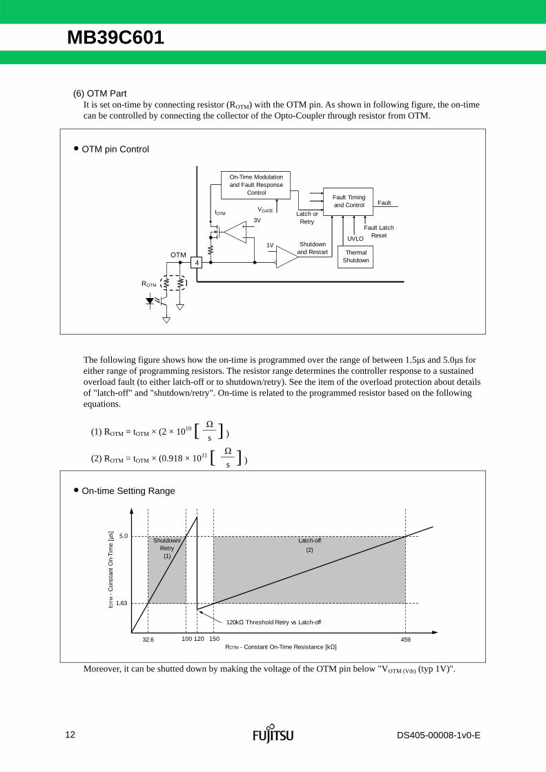
(6) OTM Part It is set on-time by connecting resistor (ROTM) with the OTM pin. As shown in following figure, the on-time can be controlled by connecting the collector of the Opto-Coupler through resistor from OTM.
OTM pin Control
On-Time Modulationand Fault Response
ControlFault Timingand Control Fault
Latch orRetry
VGATE
OTM
ROTM
4
3VIOTM
1V Shutdownand Restart Thermal
Shutdown
UVLO
Fault LatchReset
The following figure shows how the on-time is programmed over the range of between 1.5μs and 5.0μs for either range of programming resistors. The resistor range determines the controller response to a sustained overload fault (to either latch-off or to shutdown/retry). See the item of the overload protection about details of "latch-off" and "shutdown/retry". On-time is related to the programmed resistor based on the following equations.
Ω (1) ROTM = tOTM × (2 × 10¹⁰
[
s ] )
Ω(2) ROTM = tOTM × (0.918 × 10¹¹
[ s ] )
On-time Setting Range
Latch-off
(2)
Shutdown/Retry
(1)
120kΩ Threshold Retry vs Latch-off
32.6 100 120 150 459ROTM - Constant On-Time Resistance [kΩ]
tOT
M-
Con
stan
tO
n-T
ime
[µs]
1.63
5.0
Moreover, it can be shutted down by making the voltage of the OTM pin below "VOTM (Vth) (typ 1V)".

13
Limitation : development tool vendor use only FUJITSU SEMICONDUCTOR CONFIDENTIAL
DS405-00008-1v0-E
MB39C601
(7) PCL Part It is set the peak current of Primary Winding by connecting resistor with the PCL pin. The maximum peak current of Primary Side is set by connecting resistor (RPCL) between the PCL pin and GND.
100kV IDRN(pk) = (
RPCL )
An about 400ns blanking time of the beginning of switching cycle is masking the spike noise. As a result, it prevents the sense of current from malfunctioning (See the figure below.).
Peak Current Control with PCL pin
FB1
IFB
DriverVGATE
DRN6
GND7
PCL
RPCL
3
CurrentSense
IDRN
IPCL
Current Modulator
IFB, µA1
3
165 210
I DRNPK
1
3
165 210
VPCL, V
IFB, µA
IFB
tBLANKCL
FromOptocouplerEmitter
FromHigh-VoltageMOSFET Source
14
Limitation : development tool vendor use only FUJITSU SEMICONDUCTOR CONFIDENTIAL
DS405-00008-1v0-E
MB39C601
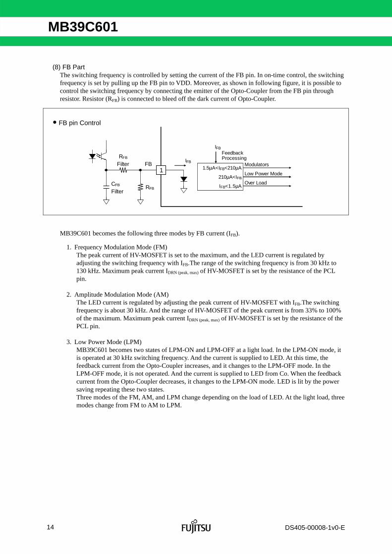
(8) FB Part The switching frequency is controlled by setting the current of the FB pin. In on-time control, the switching frequency is set by pulling up the FB pin to VDD. Moreover, as shown in following figure, it is possible to control the switching frequency by connecting the emitter of the Opto-Coupler from the FB pin through resistor. Resistor (RFB) is connected to bleed off the dark current of Opto-Coupler.
FB pin Control
FB1
IFB
1.5µA<IFB<210µA
210µA<IFB
IFB<1.5µA
Modulators
Low Power Mode
Over Load
IFBFeedbackProcessing
RFB
RFB
Filter
CFB
Filter
MB39C601 becomes the following three modes by FB current (IFB).
1. Frequency Modulation Mode (FM) The peak current of HV-MOSFET is set to the maximum, and the LED current is regulated by adjusting the switching frequency with IFB.The range of the switching frequency is from 30 kHz to 130 kHz. Maximum peak current IDRN (peak, max) of HV-MOSFET is set by the resistance of the PCL pin.
2. Amplitude Modulation Mode (AM)
The LED current is regulated by adjusting the peak current of HV-MOSFET with IFB.The switching frequency is about 30 kHz. And the range of HV-MOSFET of the peak current is from 33% to 100% of the maximum. Maximum peak current IDRN (peak, max) of HV-MOSFET is set by the resistance of the PCL pin.
3. Low Power Mode (LPM)
MB39C601 becomes two states of LPM-ON and LPM-OFF at a light load. In the LPM-ON mode, it is operated at 30 kHz switching frequency. And the current is supplied to LED. At this time, the feedback current from the Opto-Coupler increases, and it changes to the LPM-OFF mode. In the LPM-OFF mode, it is not operated. And the current is supplied to LED from Co. When the feedback current from the Opto-Coupler decreases, it changes to the LPM-ON mode. LED is lit by the power saving repeating these two states. Three modes of the FM, AM, and LPM change depending on the load of LED. At the light load, three modes change from FM to AM to LPM.

15
Limitation : development tool vendor use only FUJITSU SEMICONDUCTOR CONFIDENTIAL
DS405-00008-1v0-E
MB39C601
Switching Frequency and Peak Current Control Operation Based On FB pin
33
100
FM AM Low Power Mode
50 100 150 200 250
30
133
IFB - Feedback Current [µA]
tSW
(max
)-
Max
Sw
itchi
ngF
requ
ency
[kH
z]I D
RN
PK
(max
)-
%of
Max
Pea
kD
RN
Cur
rent
[%]
IFB, CNR1
(165µA)
IFB, CNR2
(210µA)
IFB, CNR3
(280µA)
IFB, CNR3 - IFB, CNR2
(70µA)
IFB, CNR2 - IFB, CNR1
(45µA)
IFB, LPM-HYST
(25µA)
LPM-ON LPM-OFF

16
Limitation : development tool vendor use only FUJITSU SEMICONDUCTOR CONFIDENTIAL
DS405-00008-1v0-E
MB39C601
(9) TZE Part MB39C601 requires all of the following three conditions in order to start the next switching cycle.
1. The time since the last turn-on edge must be equal to or longer than the switching time set by IFB. 2. The time since the last turn-on edge must be longer than the minimum switching period set by
MB39C601 (nominally 7.5µs which equals 133 kHz). 3. Immediately after zero energy detection at the TZE pin. Or, the time since the last zero energy
detection must be longer than tWAIT, (TZE) (2.4μs or less).
Starting switching cycle diagram
TZE≤150mV
TZE>150mV
TZE>150mV
The TZE pin is connected with Auxiliary Winding of the transformer through the resistance division, and detects zero energy as shown " TZE pin Connection".
A delay, 50ns to 200ns, can be added with CTZE to adjust the turn-on of the primary switch with the resonant bottom of Primarty Winding waveform.
Switching Waveform at detecting zero Energy
High VoltageMOSFET Drain
TZE Input
Switching Time
by IFB
Delay
Switching Time (tSW)
IDRN
CTZE - Based
Beginning Turn-on
of Next Period
VDD≥10.2V MB39C601 Enable
Startup CLK Tst = 240µs Forcing Switching
No startup Switching
Switching Freq. Timer ends
L-Edge of TZE ≤ 20mV
No L-Edge of TZE < 150mV,
TZE < 20mV
There are one or more L-Edge
of TZE ≤ 20mV, but L-Edge of
TZE ≤ 20mV is not generated
during period of 2.4µs, after
Switching Freq. Timer ends.
There are one or more L-Edge of TZE ≤ 20mV, but L-Edge of TZE ≤ 20mV is not generated during period of 2.4µs, after Switching Freq. Timer ends.
There are one or more L-Edge of TZE ≤ 20mV, but
L-Edge of TZE ≤ 20mV is not generated during
period of 2.4µs, after Switching Freq. Timer ends.
Switching Freq. Timer ends
L-Edge of TZE ≤ 20mV
Switching Freq. Timer ends L-Edge of TZE ≤ 20mV
Beginning Turn-on of
Next Period after 2.4µs
since the last TZE L-Edge

17
Limitation : development tool vendor use only FUJITSU SEMICONDUCTOR CONFIDENTIAL
DS405-00008-1v0-E
MB39C601
TZE pin Connection
CTZE
1
TZE2
RTZE2
RTZE1
NB
NP NS
5V
OVFault
20mV
Zero EnergyDetect
Fault Timingand Control

18
Limitation : development tool vendor use only FUJITSU SEMICONDUCTOR CONFIDENTIAL
DS405-00008-1v0-E
MB39C601
VARIOUS PROTECTION CIRCUITS Under voltage lockout protection (UVLO)
The under voltage lockout protection (UVLO) protects IC from malfunction and protects the system from destruction/deterioration during the transient state and momentary drop due to start up for the power supply pin voltage (VDD). The voltage decrease of the VDD pin is detected with comparator, and output HS DRIVER is turned off and output DRIVER is turned off, and the switching is stopped.The system returns if the VDD pin becomes more than the threshold voltage of the UVLO circuit.
Over voltage Proteciton (OVP) When LED is in the state of open and the output voltage rises too much, the voltage of Auxiliary Winding and the voltage of the TZE pin rise. The over voltage is detected by sampling this voltage of the TZE pin. When TZE pin voltage rises more than the threshold voltage of OVP, the over voltage is detected. Output HS DRIVER is turned off, and output DRIVER is turned off, and the switching is stopped. (latch-off)
If the VDD pin becomes below the voltage of Fault Latch Reset, OVP is released.
Over load protection (OL) When the cathode or the anode of LED is short to GND and it becomes an overloaded status at switching frequency control, the current does not flow into Rs and there is no current feedback to IFB. The current of the FB pin detects the overload with 1.5µA or less. OL state is decided to latch-off or shutdown/retry by ROTM.
Shutdown/retry … MB39C601 becomes two states of switching on for 250ms and switching off for 750ms. These states are repeated. If it is not OL status, it returns.
Latch-off … The switching is continued for 250ms. If it does not return from OL states for this period, output HS DRIVER is turned off, and output DRIVER is turned off, and the switching is stopped. If it returns from OL states after this time and the switching is still stopped (latch-off) and the VDD pin becomes below the voltage of Fault Latch Reset, Latch is released.
Over Load Protection Sequencing
1.5µA
DRN
OLNormal
Operation
ROTM = 32.6k to 100kΩ
1.5µA
NormalOperation
1.5µAIFB
IFB
DRN
OLNormal
Operation
ROTM = 150k to 459kΩ
1.5µA
NormalOperation OL
Shutdown / retry
250ms250ms
250ms 750ms 250ms 750ms
Latch - off
19
Limitation : development tool vendor use only FUJITSU SEMICONDUCTOR CONFIDENTIAL
DS405-00008-1v0-E
MB39C601
Over temperature protection (OTP) The over temperature protection (OTP) is a function to protect IC from the thermal destruction.When the junction temperature reaches +150°C,output HS DRIVER is turn off, and output DRIVER is turned off, and the switching is stopped.It returns again when the junction temperature falls to +125°C (automatic recovery).

20
Limitation : development tool vendor use only FUJITSU SEMICONDUCTOR CONFIDENTIAL
DS405-00008-1v0-E
MB39C601
VARIOUS FUNCTION TABLES DRN
Function LS_DRV HS_DRV VDD SW
Discharge SW
Detection Condition at Protected Operation
Return Condition
Remarks
Normal Operation
OFF OFF - - -
Under Voltage Lockout Protection (UVLO)
OFF OFF ON OFF VDD < 8.0V VDD > 10.2V Standby
OTM Shutdown
OFF OFF ON OFF OTM = GND OTM > 1V Standby
Over Voltage Protection (OVP)
OFF OFF ON ON TZE > 5V VDD < 6V
→ VDD > 10.2V
Latch-off
OFF OFF
Shutdown Retry OL
Timer (250ms)
Shutdown/ Retry Mode
OFF OFF ON OFF
IFB < 1.5µA 32.6k < ROTM <
100kΩ IFB > 1.5µA
Shutdown Retry Fault
(750ms)
Over Load Protection (OL)
Latch-Off Mode
OFF OFF ON ON IFB < 1.5µA
150k < ROTM < 459kΩ
VDD < 6V →
VDD > 10.2V Latch-off
Stopped state of Low Power Mode
OFF OFF ON OFF IFB > 280µA IFB < 255µA -
Over Temperature Protection (OTP)
OFF OFF ON OFF Tj > +150°C Tj < +125°C -

21
Limitation : development tool vendor use only FUJITSU SEMICONDUCTOR CONFIDENTIAL
DS405-00008-1v0-E
MB39C601
I/O PIN EQUIVALENT CIRCUIT DIAGRAM Pin No.
Pin Name
Equivalent Circuit Diagram
1 FB
FB
GND
Vref 5V
7
1
2 TZE
Vref 5V
TZE
GND 7
2
3 PCL Vref 5V
GND
PCL 3
7
4 OTM Vref 5V
GND
OTM 4
7

22
Limitation : development tool vendor use only FUJITSU SEMICONDUCTOR CONFIDENTIAL
DS405-00008-1v0-E
MB39C601
Pin No.
Pin Name
Equivalent Circuit Diagram
5 VCG
6 DRN
7
8
5
6
VCG
DRN
Vref 5V
VDD
GND

23
Limitation : development tool vendor use only FUJITSU SEMICONDUCTOR CONFIDENTIAL
DS405-00008-1v0-E
MB39C601
USAGE PRECAUTION 1. Do not configure the IC over the maximum ratings.
If the IC is used over the maximum ratings, the LSI may be permanently damaged. It is preferable for the device to normally operate within the recommended usage conditions. Usage outside of these conditions can have an adverse effect on the reliability of the LSI.
2. Use the device within the recommended operating conditions. The recommended values guarantee the normal LSI operation under the recommended operating conditions. The electrical ratings are guaranteed when the device is used within the recommended operating conditions and under the conditions stated for each item.
3. Printed circuit board ground lines should be set up with consideration for common impedance.
4. Take appropriate measures against static electricity. Containers for semiconductor materials should have anti-static protection or be made of conductive
material. After mounting, printed circuit boards should be stored and shipped in conductive bags or containers. Work platforms, tools, and instruments should be properly grounded. Working personnel should be grounded with resistance of 250 kΩ to 1 MΩ in serial between body and
ground.
5. Do not apply negative voltages. The use of negative voltages below - 0.3 V may make the parasitic transistor activated to the LSI, and can cause malfunctions.
24
Limitation : development tool vendor use only FUJITSU SEMICONDUCTOR CONFIDENTIAL
DS405-00008-1v0-E
MB39C601
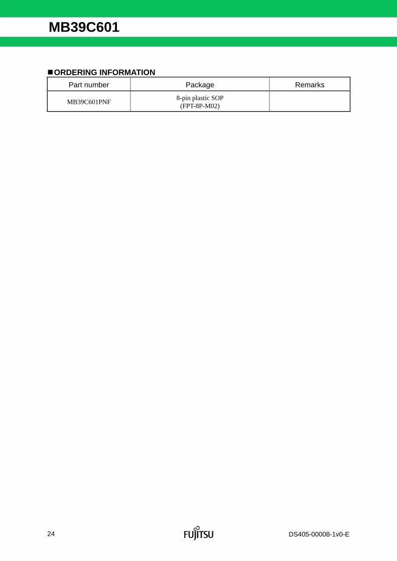
ORDERING INFORMATION
Part number Package Remarks
MB39C601PNF 8-pin plastic SOP
(FPT-8P-M02)

25
Limitation : development tool vendor use only FUJITSU SEMICONDUCTOR CONFIDENTIAL
DS405-00008-1v0-E
MB39C601
RoHS COMPLIANCE INFORMATION OF LEAD (Pb) FREE VERSION The LSI products of FUJITSU SEMICONDUCTOR with “E1” are compliant with RoHS Directive, and has observed the standard of lead, cadmium, mercury, Hexavalent chromium, polybrominated biphenyls (PBB), and polybrominated diphenyl ethers (PBDE). A product whose part number has trailing characters “E1” is RoHS compliant.
MARKING FORMAT (Lead Free version)
XXXXXXX
INDEX
Lead-free version

26
Limitation : development tool vendor use only FUJITSU SEMICONDUCTOR CONFIDENTIAL
DS405-00008-1v0-E
MB39C601
LABELING SAMPLE (Lead free version)
2006/03/01 ASSEMBLED IN JAPAN
G
QC PASS
(3N) 1MB123456P-789-GE1 1000
(3N)2 1561190005 107210
1,000 PCS
0605 - Z01A 10001/11561190005
MB123456P - 789 - GE1
MB123456P - 789 - GE1
MB123456P - 789 - GE1
Pb
Lead-free mark
JEITA logo JEDEC logo
The part number of a lead-free product has the trailing characters "E1".
"ASSEMBLED IN CHINA" is printed on the label of a product assembled in China.

27
Limitation : development tool vendor use only FUJITSU SEMICONDUCTOR CONFIDENTIAL
DS405-00008-1v0-E
MB39C601
MB39C601PNF RECOMMENDED CONDITIONS OF MOISTURE SENSITIVITY LEVEL
[FUJITSU SEMICONDUCTOR Recommended Mounting Conditions] Recommended Reflow Condition
Item Condition
Mounting Method IR (infrared reflow), warm air reflow
Mounting times 2 times
Before opening Please use it within two years after
manufacture.
From opening to the 2nd reflow Less than 8 days Storage period
When the storage period after opening was exceeded
Please process within 8 days after baking (125°C ±3°C, 24H+ 2H/0H) .Baking can be performed up to two times.
Storage conditions 5°C to 30°C, 70% RH or less (the lowest possible humidity)
[Mounting Conditions]
(1) Reflow Profile
260°C
(e)
(d')
(d)
255°C
170 °C
190 °C
RT (b)
(a)
(c)
to
(2) JEDEC Condition: Moisture Sensitivity Level 3 (IPC/JEDEC J-STD-020D)
Main heating
"H" rank : 260°C Max (a) Temperature Increase gradient : Average 1°C/s to 4°C /s (b) Preliminary heating : Temperature 170°C to 190°C, 60 s to 180 s (c) Temperature Increase gradient : Average 1°C /s to 4°C /s (d) Peak temperature : Temperature 260°C Max; 255°C or more, 10 s or less (d') Main Heating : Temperature 230°C or more, 40 s or less or Temperature 225°C or more, 60 s or less or Temperature 220°C or more, 80 s or less (e) Cooling : Natural cooling or forced cooling Note: Temperature : the top of the package bod

28
Limitation : development tool vendor use only FUJITSU SEMICONDUCTOR CONFIDENTIAL
DS405-00008-1v0-E
MB39C601
(3) Recommended manual soldering (partial heating method)
Item Condition
Before opening Within two years after manufacture
Storage period Between opening and mounting
Within two years after manufacture (No need to control moisture during the storage period because of the partial heating method.)
Storage conditions 5°C to 30°C, 70% RH or less (the lowest possible humidity)
Mounting conditions Temperature at the tip of a soldering iron: 400°C Max
Time: Five seconds or below per pin*
*: Make sure that the tip of a soldering iron does not come in contact with the package body.
(4) Recommended dip soldering
Item Condition
Mounting times 1 time
Before opening Please use it within two years after
manufacture.
From opening and mounting Less than 14 days Storage period
When the storage period after opening was exceeded
Please process within 14 days after baking (125°C ±3°C, 24H+ 2H/0H) .Baking can be performed up to two times.
Storage conditions 5°C to 30°C, 70% RH or less (the lowest possible humidity)
Mounting condition Temperature at soldering tub: 260°C Max
Time: Five seconds or below

29
Limitation : development tool vendor use only FUJITSU SEMICONDUCTOR CONFIDENTIAL
DS405-00008-1v0-E
MB39C601
PACKAGE DIMENSIONS
8-pin plastic SOP Lead pitch 1.27 mm
Package width×package length
3.9 mm × 5.05 mm
Lead shape Gullwing
Sealing method Plastic mold
Mounting height 1.75 mm MAX
Weight 0.06 g
8-pin plastic SOP(FPT-8P-M02)
(FPT-8P-M02)
C
1.27(.050)
3.90±0.30 6.00±0.20
.199–.008+.010
–0.20+0.255.05
0.13(.005) M
(.154±.012) (.236±.008)
0.10(.004)
1 4
58
0.44±0.08(.017±.003)
–0.07+0.03
0.22
.009+.001–.003
45°
0.40(.016)
"A" 0~8°
0.25(.010)
(Mounting height)
Details of "A" part
1.55±0.20(.061±.008)
0.50±0.20(.020±.008)0.60±0.15
(.024±.006)
0.15±0.10(.006±.004)(Stand off)
*1
*2
2002-2012 FUJITSU SEMICONDUCTOR LIMITED F08004S-c-5-10Dimensions in mm (inches).Note: The values in parentheses are reference values.
Note 1) 1 : These dimensions include resin protrusion.Note 2) 2 : These dimensions do not include resin protrusion.Note 3) Pins width and pins thickness include plating thickness.Note 4) Pins width do not include tie bar cutting remainder.
**
Please check the latest package dimension at the following URL. http://edevice.fujitsu.com/package/en-search/

30
Limitation : development tool vendor use only FUJITSU SEMICONDUCTOR CONFIDENTIAL
DS405-00008-1v0-E
MB39C601
MEMO

31
Limitation : development tool vendor use only FUJITSU SEMICONDUCTOR CONFIDENTIAL
DS405-00008-1v0-E
MB39C601
MEMO
32
Limitation : development tool vendor use only FUJITSU SEMICONDUCTOR CONFIDENTIAL
DS405-00008-1v0-E
MB39C601
FUJITSU SEMICONDUCTOR LIMITED Nomura Fudosan Shin-yokohama Bldg. 10-23, Shin-yokohama 2-Chome, Kohoku-ku Yokohama Kanagawa 222-0033, Japan Tel: +81-45-415-5858 http://jp.fujitsu.com/fsl/en/
For further information please contact:
North and South America FUJITSU SEMICONDUCTOR AMERICA, INC. 1250 E. Arques Avenue, M/S 333 Sunnyvale, CA 94085-5401, U.S.A. Tel: +1-408-737-5600 Fax: +1-408-737-5999 http://us.fujitsu.com/micro/ Europe FUJITSU SEMICONDUCTOR EUROPE GmbH Pittlerstrasse 47, 63225 Langen, Germany Tel: +49-6103-690-0 Fax: +49-6103-690-122 http://emea.fujitsu.com/semiconductor/ Korea FUJITSU SEMICONDUCTOR KOREA LTD. 902 Kosmo Tower Building, 1002 Daechi-Dong, Gangnam-Gu, Seoul 135-280, Republic of Korea Tel: +82-2-3484-7100 Fax: +82-2-3484-7111 http://kr.fujitsu.com/fsk/
Asia Pacific FUJITSU SEMICONDUCTOR ASIA PTE. LTD. 151 Lorong Chuan, #05-08 New Tech Park 556741 Singapore Tel : +65-6281-0770 Fax : +65-6281-0220 http://sg.fujitsu.com/semiconductor/ FUJITSU SEMICONDUCTOR SHANGHAI CO., LTD. 30F, Kerry Parkside, 1155 Fang Dian Road, Pudong District, Shanghai 201204, China Tel : +86-21-6146-3688 Fax : +86-21-6146-3660 http://cn.fujitsu.com/fss/ FUJITSU SEMICONDUCTOR PACIFIC ASIA LTD. 2/F, Green 18 Building, Hong Kong Science Park, Shatin, N.T., Hong Kong Tel : +852-2736-3232 Fax : +852-2314-4207 http://cn.fujitsu.com/fsp/
Specifications are subject to change without notice. For further information please contact each office. All Rights Reserved. The contents of this document are subject to change without notice. Customers are advised to consult with sales representatives before ordering. The information, such as descriptions of function and application circuit examples, in this document are presented solely for the purpose of reference to show examples of operations and uses of FUJITSU SEMICONDUCTOR device; FUJITSU SEMICONDUCTOR does not warrant proper operation of the device with respect to use based on such information. When you develop equipment incorporating the device based on such information, you must assume any responsibility arising out of such use of the information. FUJITSU SEMICONDUCTOR assumes no liability for any damages whatsoever arising out of the use of the information.Any information in this document, including descriptions of function and schematic diagrams, shall not be construed as license of the use or exercise of any intellectual property right, such as patent right or copyright, or any other right of FUJITSU SEMICONDUCTOR or any third party or does FUJITSU SEMICONDUCTOR warrant non-infringement of any third-party's intellectual property right or other right by using such information. FUJITSU SEMICONDUCTOR assumes no liability for any infringement of the intellectual property rights or other rights of third parties which would result from the use of information contained herein. The products described in this document are designed, developed and manufactured as contemplated for general use, including without limitation, ordinary industrial use, general office use, personal use, and household use, but are not designed, developed and manufactured as contemplated (1) for use accompanying fatal risks or dangers that, unless extremely high safety is secured, could have a serious effect to the public, and could lead directly to death, personal injury, severe physical damage or other loss (i.e., nuclear reaction control in nuclear facility, aircraft flight control, air traffic control, mass transport control, medical life support system, missile launch control in weapon system), or (2) for use requiring extremely high reliability (i.e., submersible repeater and artificial satellite). Please note that FUJITSU SEMICONDUCTOR will not be liable against you and/or any third party for any claims or damages arising in connection with above-mentioned uses of the products. Any semiconductor devices have an inherent chance of failure. You must protect against injury, damage or loss from such failures by incorporating safety design measures into your facility and equipment such as redundancy, fire protection, and prevention of over-current levels and other abnormal operating conditions. Exportation/release of any products described in this document may require necessary procedures in accordance with the regulations of the Foreign Exchange and Foreign Trade Control Law of Japan and/or US export control laws. The company names and brand names herein are the trademarks or registered trademarks of their respective owners.
Edited: Sales Promotion Department