Dry Transient Electronic Systems by Use of Materials that ... of Illinois at Urbana-Champaign...
8
FULL PAPER © 2017 WILEY-VCH Verlag GmbH & Co. KGaA, Weinheim wileyonlinelibrary.com (1 of 8) 1606008 1. Introduction The emerging field of transient electronics relies on the development of materials and device architectures that undergo controlled, physical self-elimination by processes ranging from water dissolution to enzymatic degradation to depolymeri- zation to mechanical fragmentation. [1–5] Such features are of interest for applica- tions not well served by conventional tech- nologies, such as temporary biomedical implants, [6–11] resorbable environmental monitors, [12] physically secure data storage systems, [13–15] and nonrecoverable sensitive electronics. [16–20] Most work in transient electronics involves the development of sys- tems that dissolve or are physically altered by the action of wet chemistries. Examples include biodegradable electronics, where Dry Transient Electronic Systems by Use of Materials that Sublime Bong Hoon Kim, Jae-Hwan Kim, Luana Persano, Suk-Won Hwang, Seungmin Lee, Jungyup Lee, Yongjoon Yu, Yongseon Kang, Sang M. Won, Jahyun Koo, Youn Kyoung Cho, Gyum Hur, Anthony Banks, Jun-Kyul Song, Phillip Won, Young Min Song, Kyung-In Jang, Daeshik Kang, Chi Hwan Lee, Dario Pisignano, and John A. Rogers* The recent emergence of materials for electronic systems that are capable of programmable self-destruction and/or bio/eco-resorption creates the potential for important classes of devices that cannot be easily addressed using conventional technologies, ranging from temporary biomedical implants to enviromentally benign environmental monitors to hardware secure data systems. Although most previous demonstrations rely on wet chemistry to initiate transient processes of degradation/decomposition, options in “dry transient electronic systems” could expand the range of possible uses. The work presented here introduces materials and composite systems in which sublimation under ambient conditions leads to mechanical fragmentation and disintegration of active devices upon disappearance of a supporting substrate, encapsulation layer, interlayer dielectric and/or gate dielectric. Examples span arrays of transistors based on silicon nanomembranes with specialized device designs to solar cells adapted from commercial components. DOI: 10.1002/adfm.201606008 Dr. B. H. Kim, Prof. J. A. Rogers Departments of Materials Science and Engineering Biomedical Engineering, Chemistry, Neurological Surgery Mechanical Engineering, Electrical Engineering and Computer Science Simpson Querrey Institute and Feinberg Medical School Center for Bio-Integrated Electronics Northwestern University Evanston, IL 60208, USA E-mail: [email protected] J.-H. Kim, Dr. S. Lee, J. Lee, Y. Yu, Y. Kang, S. M. Won, Dr. J. Koo, Y. K. Cho, G. Hur, A. Banks, J.-K. Song, P. Won Department of Materials Science and Engineering Frederick Seitz Materials Research Laboratory University of Illinois at Urbana-Champaign Urbana, IL 61801, USA Dr. L. Persano, Prof. D. Pisignano NEST Istituto Nanoscienze-CNR Piazza S. Silvestro 12, I-56127 Pisa, Italy Prof. S.-W. Hwang KU-KIST Graduate School of Converging Science and Technology Korea University Seoul 02841, Republic of Korea Prof. Y. M. Song School of Electrical Engineering and Computer Science Gwangju Institute of Science and Technology (GIST) Gwangju 61005, Republic of Korea Prof. K.-I. Jang Department of Robotics Engineering Daegu Gyeongbuk Institute of Science and Technology (DGIST) Daegu 42988, Republic of Korea Prof. D. Kang Department of Mechanical Engineering Ajou University Suwon 443–749, Republic of Korea Prof. C. H. Lee Weldon School of Biomedical Engineering School of Mechanical Engineering The Center for Implantable Devices, and Birck Nanotechnology Center Purdue University West Lafayette, IN 47907, USA Prof. D. Pisignano Dipartimento di Matematica e Fisica “Ennio De Giorgi” Università del Salento Via Arnesano, I-73100 Lecce, Italy www.afm-journal.de Adv. Funct. Mater. 2017, 1606008 www.advancedsciencenews.com
Transcript of Dry Transient Electronic Systems by Use of Materials that ... of Illinois at Urbana-Champaign...

FULL P
APER
© 2017 WILEY-VCH Verlag GmbH & Co. KGaA, Weinheim wileyonlinelibrary.com (1 of 8) 1606008
1. Introduction
The emerging field of transient electronics relies on the development of materials and device architectures that undergo controlled, physical self-elimination by processes ranging from water dissolution to enzymatic degradation to depolymeri-zation to mechanical fragmentation.[1–5] Such features are of interest for applica-tions not well served by conventional tech-nologies, such as temporary biomedical implants,[6–11] resorbable environmental monitors,[12] physically secure data storage systems,[13–15] and nonrecoverable sensitive electronics.[16–20] Most work in transient electronics involves the development of sys-tems that dissolve or are physically altered by the action of wet chemistries. Examples include biodegradable electronics, where
Dry Transient Electronic Systems by Use of Materials that Sublime
Bong Hoon Kim, Jae-Hwan Kim, Luana Persano, Suk-Won Hwang, Seungmin Lee, Jungyup Lee, Yongjoon Yu, Yongseon Kang, Sang M. Won, Jahyun Koo, Youn Kyoung Cho, Gyum Hur, Anthony Banks, Jun-Kyul Song, Phillip Won, Young Min Song, Kyung-In Jang, Daeshik Kang, Chi Hwan Lee, Dario Pisignano, and John A. Rogers*
The recent emergence of materials for electronic systems that are capable of programmable self-destruction and/or bio/eco-resorption creates the potential for important classes of devices that cannot be easily addressed using conventional technologies, ranging from temporary biomedical implants to enviromentally benign environmental monitors to hardware secure data systems. Although most previous demonstrations rely on wet chemistry to initiate transient processes of degradation/decomposition, options in “dry transient electronic systems” could expand the range of possible uses. The work presented here introduces materials and composite systems in which sublimation under ambient conditions leads to mechanical fragmentation and disintegration of active devices upon disappearance of a supporting substrate, encapsulation layer, interlayer dielectric and/or gate dielectric. Examples span arrays of transistors based on silicon nanomembranes with specialized device designs to solar cells adapted from commercial components.
DOI: 10.1002/adfm.201606008
Dr. B. H. Kim, Prof. J. A. RogersDepartments of Materials Science and EngineeringBiomedical Engineering, Chemistry, Neurological Surgery Mechanical Engineering, Electrical Engineering and Computer ScienceSimpson Querrey Institute and Feinberg Medical SchoolCenter for Bio-Integrated ElectronicsNorthwestern UniversityEvanston, IL 60208, USAE-mail: [email protected]. Kim, Dr. S. Lee, J. Lee, Y. Yu, Y. Kang, S. M. Won, Dr. J. Koo, Y. K. Cho, G. Hur, A. Banks, J.-K. Song, P. WonDepartment of Materials Science and EngineeringFrederick Seitz Materials Research LaboratoryUniversity of Illinois at Urbana-ChampaignUrbana, IL 61801, USADr. L. Persano, Prof. D. PisignanoNESTIstituto Nanoscienze-CNRPiazza S. Silvestro 12, I-56127 Pisa, ItalyProf. S.-W. HwangKU-KIST Graduate School of Converging Science and TechnologyKorea UniversitySeoul 02841, Republic of Korea
Prof. Y. M. SongSchool of Electrical Engineering and Computer ScienceGwangju Institute of Science and Technology (GIST)Gwangju 61005, Republic of KoreaProf. K.-I. JangDepartment of Robotics EngineeringDaegu Gyeongbuk Institute of Science and Technology (DGIST)Daegu 42988, Republic of KoreaProf. D. KangDepartment of Mechanical EngineeringAjou UniversitySuwon 443–749, Republic of KoreaProf. C. H. LeeWeldon School of Biomedical EngineeringSchool of Mechanical EngineeringThe Center for Implantable Devices, and Birck Nanotechnology CenterPurdue UniversityWest Lafayette, IN 47907, USAProf. D. PisignanoDipartimento di Matematica e Fisica “Ennio De Giorgi” Università del SalentoVia Arnesano, I-73100 Lecce, Italy
www.afm-journal.de
Adv. Funct. Mater. 2017, 1606008
www.advancedsciencenews.com

FULL
PAPER
© 2017 WILEY-VCH Verlag GmbH & Co. KGaA, Weinheimwileyonlinelibrary.com1606008 (2 of 8)
dissolution in biofluids eliminates device load on the body and self-destructing devices with cointegrated triggerable microflu-idic systems that contain etchants.[16,18,21] Certain applications could, however, benefit from transient operation in environ-ments where there is little or no ambient water or moisture, such as in the desert, at high altitudes, or in space, using device designs that avoid the need for microfluidics.
This paper presents materials and device designs for forms of transient electronics that undergo timed self-destruction induced by ambient sublimation of a supporting substrate, encapsulation layer, interlayer dielectric, and/or gate dielectric followed by resulting fragmentation of the remaining, ultrathin components of the circuit.[22] Such “dry” operation provides capabilities that complement those of more widely explored “wet” systems. Examples of these approaches include transis-tors and solar cells formed by transfer printing ultrathin, pre-formed silicon devices onto sublimating substrates, including demonstrations where the same material also serves as the dielectric layers. Sublimation leads to disintegration of the remaining materials into microscopic fragments due to loss of mechanical support and/or adjoining films. Cyclododecane (CDD), sometimes utilized as a temporary layer to protect fragile and sensitive surfaces during archeological recovery,[23,24] provides an excellent material for such purposes due to its low melting point (90 °C), high vapor pressure (0.1 hPa) at room temperature, and low viscosity at elevated temperatures (2.2 mPaS@95 °C). Other examples of materials include men-thol, camphor, perfluorododecane, and hexamethylcyclotrisi-loxane. Composites based on embedded nanoparticles provide a means to control the rate of sublimation by modulating the exposed interfacial area.
The dry mode of transience in the technology presented here has several advantages compared to wet alternatives: it avoids (1) the need for external or internal sources of liquid reactants whose availability might be limited either by the nature of the surrounding environment or the difficulty in forming hermeti-cally sealed, integrated microfluidic reservoirs, (2) challenges in semiconductor processing of materials that are susceptible to liquid exposure, and (3) variability in dissolution/reaction rates due to uncontrolled flows of dissolving liquids. The combina-tion of wet and dry approaches could create additional possi-bilities, where sublimating materials—many of which have extremely low water solubility and permeability rates—serve as an encapsulating layer for wet transient devices.
2. Results and Discussion
Applying mechanical forces to crystal grains (sample mass in the decigram range) can yield free-standing films of waxy sub-limating solids. Specifically, forces of 50–60 kN applied for 10–30 min through a two-column precision manual press at room temperature activate material transport and grain melting to facilitate film formation. Depending on the force, processing time ,and amount of starting material, films with 500–700 µm thickness and 3–4 cm diameter can be achieved in this manner.
Many factors, including thickness, shape, exposed surface area, and ambient conditions such as temperature and air venti-lation, affect the rate of sublimation in a material such as CDD.
The role of ventilation can be assessed by placing samples with identical shapes and masses under a fume hood under stable ambient conditions (temperature: 21 °C; humidity: 30%–40%), varying the face velocity of the hood through the position of the front sash, and measuring the sample thickness (at the center) and mass at several times (Figure 1a). Data collected under ambient laboratory conditions serve as points of com-parison (black dots in Figure 1a). In the absence of ventilation, the sublimation rate is about 1.3 µm h−1. This rate increases to 4.6 µm h−1 under ventilation with an air velocity of 1.9 m s−1. The corresponding mass losses are of 0.7 and 4 mg h−1, respec-tively (data linear fitting for 0 ≤ t ≤ 70 h). Photographs in the inset of Figure 1a display the morphological and dimensional changes of CDD samples, stored at the highest ventilation rate tested here.
An effective strategy to reduce the sublimation rate involves addition of titanium dioxide nanoparticles (TiO2 NPs, average diameter: 10 nm) with concentrations in the range 3%–15% w/w in the CDD. The result reduces the sublima-tion rate by a factor of 3 for the 15% w/w case during the first 100 h for samples that have a total surface area of ≈20 cm2 and a mass of ≈0.3 g (Figure 1b). Sublimation proceeds rapidly at the edges, and NPs deposit on the supporting substrate as the CDD disappears. For times beyond ≈100 h, the sublimation rate further decreases, particularly for formulations that involve high NP loading. After 500 h, the thicknesses of CDD samples doped with NPs at 8% are roughly twice as large as those of pure CDD. Photographs that capture the time dependence of the morphologies of samples with different NPs content appear in Figure 1c. The inclusion of NPs might reduce the mesoscale extension of more volatile, superficial molecular layers, and compete with sublimation by hydrophobic–hydrophobic inter-actions with the wax molecules, thus leading to sublimation enthalpy increase and to a reduced rate of mass loss.
A range of other materials can also be considered, as summarized in Figure 1d–g and Figures S1–3 (Supporting Information). For instance, menthol exhibits sublimation rates comparable to CDD (1.6 µm h−1), with values that are also strongly reduced by the addition of NPs (up to five times for 8% w/w doped samples). The inclusion of NPs appears to be a generally applicable strategy to reduce the sublimation rate.
The fabrication of dry transient electronic devices involves conventional microfabrication processes (e.g., thermal annealing, deposition, etching, and lithographic patterning) conducted prior to integration of the sublimating substrates or dielectric layers. This scheme is valuable because most subli-mating materials of interest for present purposes sublimate quickly and completely at 100 °C and continuously even under ambient temperature and pressure, thereby severely limiting the ability to perform any form of high temperature or vacuum pro-cessing. Figure 2a presents a schematic illustration of the pro-cess flow. The first step yields a temporary, or handle, substrate by thermally curing a spin-cast layer of diluted polydimethyl-siloxane (PDMS) (monomer: cross-linker: hexane: 10: 1: 10, weight ratio, 3000 rpm) on a glass wafer. Next, spin-casting and curing a layer of polyimide (PI: ≈ 6 µm; Sigma-Aldrich, Inc.) form a temporary support. Transfer printing delivers a collec-tion of silicon nanomembranes (Si NMs, ≈200 nm) with pat-terned regions of doping onto the PI layer in spatial layouts that
Adv. Funct. Mater. 2017, 1606008
www.afm-journal.de www.advancedsciencenews.com

FULL P
APER
© 2017 WILEY-VCH Verlag GmbH & Co. KGaA, Weinheim wileyonlinelibrary.com (3 of 8) 1606008
match device requirements.[27,28] Photolithography followed by reactive ion etching (RIE; SF6, 50 mtorr, 100 W, 40 sccm, and 120 s) structures the membranes to leave only silicon in the active regions of the devices. Plasma-enhanced chemical vapor deposition (PECVD) of SiO2 (100 nm) forms the gate
oxide layer, patterned by photolithography and buffered oxide etching. Electron beam evaporation of Au/Cr (≈100/5 nm) fol-lowed by photolithography and wet etching defines electrodes and interconnects. Spin-casting a thin film of a fluoropolymer (6 µm, OSCoR 2312 photoresist solution, Orthogonal, Inc.)
Adv. Funct. Mater. 2017, 1606008
www.afm-journal.dewww.advancedsciencenews.com
Figure 1. Rate of sublimation of CDD and dependence on loading ratio of TiO2 nanoparticles (NPs). The plots show thickness (top panel) and weight (bottom panel) of free-standing films made with different compositions and under different conditions. In all cases, data are normalized to the initial values. In the images, all scale bars are 1.5 cm. a) CDD films stored under a fume hood at different face velocities. Data collected at typical laboratory conditions serve as comparisons (insets: photographs of a film stored at 1.9 m s−1, at different times. From left to right: photograph of a just-produced sample, and after 24, 70, and 95 h, respectively). b) Pure CDD film and various CDD composites with TiO2 NPs stored under a fume hood at 0 m s−1 face velocity (insets: photographs of representative samples. From left to right: TiO2/CCD: 3%, 8%, and 15% w/w, respectively). c) Photographs of composite films at different times. d) Menthol and menthol/TiO2 NP films stored under a fume hood at 0 m s−1 face velocity (insets: photographs of representative samples. From left to right: pure menthol, TiO2/menthol: 3%, and TiO2/menthol: 8% w/w, respectively). e) Camphor and camphor/TiO2 NP films stored under a fume hood at 0 m s−1 face velocity (insets: photographs of representative samples. From left to right: pure camphor, TiO2/camphor: 3%, and TiO2/camphor: 8% w/w, respectively). f) Perfluorododecane and perfluorododecane/TiO2 NP films stored under a fume hood at 0 m s−1 face velocity (insets: photographs of representative samples. From left to right: pure perfluorododecane, TiO2/perfluorododecane: 3% and TiO2/perfluorododecane: 8% w/w, respectively). g) Hexamethylcyclotrisiloxane and hexamethylcyclotrisiloxane/TiO2 NP films stored under a fume hood at 0 m s−1 face velocity (insets: photographs of representative samples. From left to right: pure hexamethylcyclotrisiloxane: 3% and TiO2/hexamethylcyclotrisiloxane: 8% w/w, respectively).

FULL
PAPER
© 2017 WILEY-VCH Verlag GmbH & Co. KGaA, Weinheimwileyonlinelibrary.com1606008 (4 of 8)
onto the entire device stack allows retrieval onto a water-soluble cellulose tape. This layer is important because it conformally embeds the devices into its near surface region.[29] The very
low strength of adhesion between the PI and PDMS greatly enhances the yield of retrieval.[30] Next, RIE (O2 gas, 200 mtorr, 150 W, and 20 sccm) eliminates the PI from the bottom while
Adv. Funct. Mater. 2017, 1606008
www.afm-journal.de www.advancedsciencenews.com
Figure 2. Materials and procedures for fabricating dry transient electronic circuits on substrates that sublime. a) Schematic illustrations of the steps for fabrication. The process begins with a silicon nanomembrane (Si NM) on a handle substrate with patterns of doping in the configuration of the array (upper left). Deposition and patterning of a gate oxide and set of electrodes defines nMOS transistors (upper middle). Retrieving the array using a water-soluble tape allows exposure and removal of the bottom layer of polyimide by reactive ion etching (right). Transfer printing onto a CDD substrate (lower middle) and removing the fluoropolymer complete the process (lower left). b) Optical microscopic images of an Si NM on polyimide (left), after gate oxide deposition and metallization (middle); an array of transistors on a substrate of CDD (right). c) Linear and log scale plots of the transfer curves, and d) current–voltage characteristics of a representative device (channel length/width: 15/80 µm).

FULL P
APER
© 2017 WILEY-VCH Verlag GmbH & Co. KGaA, Weinheim wileyonlinelibrary.com (5 of 8) 1606008
the structure remains adhered to the cellulose.[31] The final pair of steps involves transfer onto a CDD substrate (diameter 1.5 cm, thickness 4–5 mm) formed by pouring molten CDD into a metal mold, and removing the cellulose and the fluoropolymer by immersion in deionized water and stripper solution (Orthog-onal stripper 700 solution, Orthogonal, Inc.),[32] respectively.
Optical micrographs in Figure 2b show (i) doped Si NM transfer printed onto PI, (ii) patterned Cr/Au metallization, and (iii) an array of n-channel metal-oxide-semiconductor field-effect transistors (MOSFETs) on CDD. As the CDD sublimes, the mechanical support for the fragile, ultrathin device struc-tures disappears, thereby leading to their mechanical fracture and fragmentation under naturally occurring, ambient environ-mental conditions (e.g., wind and rain).
The electrical properties (Figure 2c, linear and log scale plots of the transfer curves; Figure 2d, current–voltage characteris-tics) of a representative n-channel MOSFET with L (channel length): 15 µm and W (channel width): 80 µm indicate on/off ratios of 105, saturation and linear regime mobilities of ≈400 and ≈500 cm2 V−1s−1, respectively (Figure 2c; Figure S4, Supporting Information). Current–voltage characteristics meas-ured at various gate biases (0–5 V) are shown in Figure 2d. These electrical behaviors are similar to those of analogous devices on nontransient, rigid substrates.[31]
Figure 3a,b shows a time sequence of top and tilted-view images that illustrate the disintegration of a 5 × 5 array of transistors upon sublimation of the CDD in a dry environ-ment at elevated temperature (60 °C, humidity: 25%,). Within ≈12 d, the CDD substrate largely disappears and the supported electronics fragment into pieces with characteristic sizes of 200–300 µm, likely due to ambient air flow and rates of subli-mation that vary across the substrate according to the local cov-erage of the overlying electronic layers. Figure 3b shows that a peak forms at the center regions of each silicon device as time passes (red-dotted line at the center of Figure 3b). This effect follows from limited air exposure of the CDD that lies beneath the source, drain, and gate electrodes, which have dimensions that are relatively large compared to those of the intercon-nects. These differences lead to spatial variations in the rate of undercut removal of the CDD.
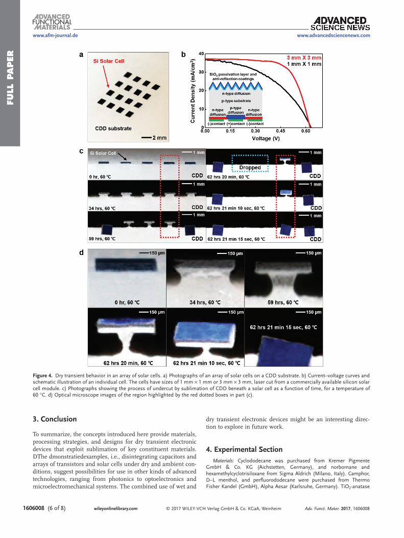
An important aspect of these ideas is that they are com-patible with commercial components, as shown in Figure 4a, for the case of a silicon solar cell module (DIY Professional Mono Sunpower Solar Cell, Dig Dog Bone Inc.). Here, laser dicing (see the Experimental Section) divides the module into small pieces to facilitate fragmentation in the transience process. Figure 4b shows the efficiencies of cells with dimen-sions of 1 mm × 1 mm (Voc: 0.63 V; Jsc: 36.97 mA cm−2; fill factor: 45%; Eff.: 10.4%) and 3 mm × 3 mm (Voc: 0.62 V; Jsc: 37.2 mA cm−2; fill factor: 68%; Eff.: 15.68%) formed in this manner, along with a schematic illustration. Figure 4c pre-sents photographs that capture the time evolution of the sub-limation of a CDD substrate for these components. Figure 4d is an enlarged image that corresponds to the region high-lighted by the red-dotted line in Figure 4c. Within 3 d, the cells collapse as the CDD disappears. By contrast to the tran-sistors and interconnects described previously, these solar cells are sufficiently rigid that they do not bend or fracture, as shown in Figure 4d, such that air can transport underneath the devices throughout most of the undercut process. The
cells begin to tilt as the sublimation proceeds such that dis-integration occurs due to failure of the interconnects, at rates that exceed those of the devices in Figure 3, where bending of the layers frustrates free access of air to the underlying CDD surfaces.
Sublimating materials can also be used as functional layers. Figure 5a shows an example of a variable capacitor, in which a layer of CDD with a thickness of 70–100 µm serves as the dielectric and Mg serves as the electrodes (bottom electrode: 2 µm; top electrode: 20 µm). Sublimation causes the capaci-tance to vary over time, as summarized in Figure 5b,c. The capacitance decreases by 0.07 pF within 40 h and by another 0.12 pF over the following 20 h. This mode, in which critical layers of the devices themselves disappear, provides additional options in the use of sublimation for transient devices.
Adv. Funct. Mater. 2017, 1606008
www.afm-journal.dewww.advancedsciencenews.com
Figure 3. Microscopic images of disintegration of an array of transistors as a result of sublimation of a supporting substrate of CDD. a) Images that illustrate the process of self-destruction after 1, 4, 10, and 12 d, at a temperature of 60 °C. b) Additional images corresponding to each case in part (a).
FULL
PAPER
© 2017 WILEY-VCH Verlag GmbH & Co. KGaA, Weinheimwileyonlinelibrary.com1606008 (6 of 8) Adv. Funct. Mater. 2017, 1606008
www.afm-journal.de www.advancedsciencenews.com
3. Conclusion
To summarize, the concepts introduced here provide materials, processing strategies, and designs for dry transient electronic devices that exploit sublimation of key constituent materials. DThe dmonstratiedexamples, i.e., disintegrating capacitors and arrays of transistors and solar cells under dry and ambient con-ditions, suggest possibilities for use in other kinds of advanced technologies, ranging from photonics to optoelectronics and microelectromechanical systems. The combined use of wet and
dry transient electronic devices might be an interesting direc-tion to explore in future work.
4. Experimental SectionMaterials: Cyclododecane was purchased from Kremer Pigmente
GmbH & Co. KG (Aichstetten, Germany), and norbornane and hexamethylcyclotrisiloxane from Sigma Aldrich (Milano, Italy). Camphor, D–L menthol, and perfluorododecane were purchased from Thermo Fisher Kandel (GmbH), Alpha Aesar (Karlsruhe, Germany). TiO2-anatase
Figure 4. Dry transient behavior in an array of solar cells. a) Photographs of an array of solar cells on a CDD substrate. b) Current–voltage curves and schematic illustration of an individual cell. The cells have sizes of 1 mm × 1 mm or 3 mm × 3 mm, laser cut from a commercially available silicon solar cell module. c) Photographs showing the process of undercut by sublimation of CDD beneath a solar cell as a function of time, for a temperature of 60 °C. d) Optical microscope images of the region highlighted by the red dotted boxes in part (c).

FULL P
APER
© 2017 WILEY-VCH Verlag GmbH & Co. KGaA, Weinheim wileyonlinelibrary.com (7 of 8) 1606008Adv. Funct. Mater. 2017, 1606008
www.afm-journal.dewww.advancedsciencenews.com
powder (99%, 10 nm) was purchased from Nanostructured and Amorphous Materials, Inc. (Houston, USA).
Fabrication of Dry Transient Silicon nMOS Transistors: Phosphorus doping at 950 °C defined highly doped areas for source and drain contacts on n-type silicon on insulator (SOI, top silicon ≈300 nm, SOITEC, France) wafers for n-type transistors. Removal of the buried oxide by wet etching with HF released the top device silicon from the SOI, and enabled transfer printing of the resulting Si NMs onto spin-casted films of polyimide/PDMS on a glass carrier substrate. Patterned regions of silicon resulted from RIE (Plasmatherm) with sulfur hexafluoride (SF6) gas. A thin layer of SiO2 (≈100 nm) formed by PECVD served as the gate dielectric. Etching openings in this layer using a buffered oxide etchant (Transene Company, Inc., USA) defined contact pads for source and drain electrodes. A 100/5 nm layer of Au/Cr, deposited by electron beam evaporation, was used for source, drain, gate electrodes, as well as interconnects. After metallization, spin casting yielded a thin film of a fluoropolymer (6 µm, OSCoR 2312 Photoresist Solution, Orthogonal, Inc.) across the entire sample. After retrieving the device stack with a water-soluble cellulose tape, RIE using oxygen (O2) gas removed the bottom layer of polyimide. Transfer printing delivered the device stacks onto a CDD substrate. Finally, DI water and stripper solution (Orthogonal stripper 700 solution, Orthogonal, Inc.) removed the water-soluble tape and fluoropolymer layer, respectively.
Fabrication of Dry Transient Silicon Solar Cells: Commercially available solar cell modules (DIY Professional Mono Sunpower Solar Cell, Dig Dog Bone, Inc.) were laser cut (diode pumped IR laser, wavelength: 790–820 nm; power: 0.5–1 W; pulse width: 15 ns; 20 times) into
1 mm × 1 mm and 3 mm × 3 mm sizes. Transfer printing delivered these components onto a CDD substrate heated to its glass temperature.
Fabrication of Dry Transient Capacitors: Photolithographic patterning of a film (≈2 µm thick) of Mg evaporated onto a clean silicon wafer defined bottom electrodes. Spray coating formed a uniform film of CDD. A mm-scale Mg metal film (≈20 µm) physically laminated on top served as the top electrode.
Supporting InformationSupporting Information is available from the Wiley Online Library or from the author.
AcknowledgementsB.H.K., J.-H.K., L.P., and S.-W.H. contributed equally to this work. This research was supported by the Defense Advanced Research Projects Agency (DARPA). S.-W.H. was supported by the Basic Science Research Program through the National Research Foundation of Korea (NRF) funded by the Ministry of Education (Grant NRF-2015R1C1A1A02037560).
Received: November 15, 2016Revised: December 16, 2016
Published online:
Figure 5. Dry transient capacitor that uses a sublimating dielectric layer. a) Photograph of a device composed of Mg top/bottom electrodes and a CDD dielectric layer. The device self-destructs by sublimation at ambient conditions. b,c) Plot of the capacitance as a function of time and graphs of voltage–capacitance at three representative times.

FULL
PAPER
© 2017 WILEY-VCH Verlag GmbH & Co. KGaA, Weinheimwileyonlinelibrary.com1606008 (8 of 8) Adv. Funct. Mater. 2017, 1606008
www.afm-journal.de www.advancedsciencenews.com
[1] M. Muskovich, C. J. Bettinger, Adv. Healthcare Mater. 2012, 1, 248.[2] C. J. Bettinger, Z. Bao, Polym. Int. 2010, 59, 563.[3] M. Irimia-Vladu, N. S. Sariciftci, S. Bauer, J. Mater. Chem. 2011, 21,
1350.[4] S. Hwang, J. A. Rogers, Science 2013, 337, 1640.[5] C. J. Bettinger, Trends Biotechnol. 2015, 33, 575.[6] H. Tao, S.-W. Hwang, B. Marelli, B. An, J. E. Moreau, M. Yang,
M. A. Brenckle, S. Kim, D. L. Kaplan, J. A. Rogers, F. G. Omenetto, Proc. Natl. Acad. Sci. USA 2014, 111, 17385.
[7] H. Tao, S. W. Hwang, B. Marelli, B. An, J. E. Moreau, M. Yang, M. A. Brenckle, S. Kim, D. L. Kaplan, J. A. Rogers, F. G. Omenetto, in 2015 28th IEEE Int. Conf. Micro Electro Mech. Syst. (Eds: J. Brugger, W. van der Wijngaart), IEEE 2015, p. 168.
[8] D. Son, J. Lee, D. J. Lee, R. Ghaffari, S. Yun, S. J. Kim, J. E. Lee, H. R. Cho, S. Yoon, S. Yang, S. Lee, S. Qiao, D. Ling, S. Shin, J. K. Song, J. Kim, T. Kim, H. Lee, J. Kim, M. Soh, N. Lee, C. S. Hwang, S. Nam, N. Lu, T. Hyeon, S. H. Choi, D. H. Kim, ACS Nano 2015, 9, 5937.
[9] Y. J. Kim, S.-E. Chun, J. Whitacre, C. J. Bettinger, J. Mater. Chem. B 2013, 1, 3781.
[10] C. H. Lee, H. Kim, D. V Harburg, G. Park, Y. Ma, T. Pan, J. S. Kim, N. Y. Lee, B. H. Kim, K.-I. Jang, S.-K. Kang, Y. Huang, J. Kim, K.-M. Lee, C. Leal, J. A. Rogers, NPG Asia Mater. 2015, 7, e227.
[11] C. J. Bettinger, Macromol. Biosci. 2011, 11, 467.[12] X. Huang, Y. Liu, S. W. Hwang, S. K. Kang, D. Patnaik, J. F. Cortes,
J. A. Rogers, Adv. Mater. 2014, 26, 7371.[13] H. Tao, B. Marelli, M. Yang, B. An, M. S. Onses, J. A. Rogers,
D. L. Kaplan, F. G. Omenetto, Adv. Mater. 2015, 27, 4273.[14] S. W. Hwang, S. K. Kang, X. Huang, M. A. Brenckle, F. G. Omenetto,
J. A. Rogers, Adv. Mater. 2015, 27, 47.[15] L. Yin, C. Bozler, D. V. Harburg, F. Omenetto, J. A. Rogers, Appl.
Phys. Lett. 2015, 106, 014105.[16] H. Acar, S. Çinar, M. Thunga, M. R. Kessler, N. Hashemi,
R. Montazami, Adv. Funct. Mater. 2014, 24, 4135.[17] M. Irimia-Vladu, E. D. Gåowacki, P. A. Troshin, G. Schwabegger,
L. Leonat, D. K. Susarova, O. Krystal, M. Ullah, Y. Kanbur, M. A. Bodea, V. F. Razumov, H. Sitter, S. Bauer, N. S. Sariciftci, Adv. Mater. 2012, 24, 375.
[18] Y. Chen, R. Jamshidi, K. White, S. Çınar, E. Gallegos, N. Hashemi, R. Montazami, J. Polym. Sci., Part B: Polym. Phys. 2016, 54, 2021.
[19] M. Irimia-Vladu, P. A. Troshin, M. Reisinger, L. Shmygleva, Y. Kanbur, G. Schwabegger, M. Bodea, R. Schwödiauer, A. Mumyatov, J. W. Fergus, V. F. Razumov, H. Sitter, N. S. Sariciftci, S. Bauer, Adv. Funct. Mater. 2010, 20, 4069.
[20] C. J. Bettinger, Z. Bao, Adv. Mater. 2010, 22, 651.[21] C. H. Lee, J. W. Jeong, Y. Liu, Y. Zhang, Y. Shi, S. K. Kang, J. Kim,
J. S. Kim, N. Y. Lee, B. H. Kim, K. I. Jang, L. Yin, M. K. Kim, A. Banks, U. Paik, Y. Huang, J. A. Rogers, Adv. Funct. Mater. 2015, 25, 1338.
[22] A. Hense, C. Fromm, D. Zielke, Procedia Eng. 2010, 5, 713.[23] M. Teresa, D. Carbó, J. De, C. Cañizares, J. Anal. and Appl. Pyrol.
2008, 85, 470.[24] S. Muñoz-Viñas, V. Vivancos-Ramón, P. Ruiz-Segura, Restaurator
2016, 37, 29.[25] L. Persano, S. Molle, S. Girardo, A. A. R. Neves, A. Camposeo,
R. Stabile, R. Cingolani, D. Pisignano, Adv. Funct. Mater. 2008, 18, 2692.
[26] H. J. Choi, S. G. Kim, Y. H. Hyun, M. S. Jhon, Macromol. Rapid Commun. 2001, 22, 320.
[27] A. Carlson, A. M. Bowen, Y. Huang, R. G. Nuzzo, J. A. Rogers, Adv. Mater. 2012, 24, 5284.
[28] M. A. Meitl, Z.-T. Zhu, V. Kumar, K. J. Lee, X. Feng, Y. Y. Huang, I. Adesida, R. G. Nuzzo, J. A. Rogers, Nat. Mater. 2006, 5, 33.
[29] B. H. Kim, S. Nam, N. Oh, S. Y. Cho, K. J. Yu, C. H. Lee, J. Zhang, K. Deshpande, P. Trefonas, J. H. Kim, J. Lee, J. H. Shin, Y. Yu, J. Bin Lim, S. M. Won, Y. K. Cho, N. H. Kim, K. J. Seo, H. Lee, T. Il Kim, M. Shim, J. A. Rogers, ACS Nano 2016, 10, 4920.
[30] J.-H. Moon, D. H. Baek, Y. Y. Choi, K. H. Lee, H. C. Kim, S.-H. Lee, J. Micromech. Microeng. 2010, 20, 25032.
[31] S. W. Hwang, D. H. Kim, H. Tao, T. Kim Il, S. Kim, K. J. Yu, B. Panilaitis, J. W. Jeong, J. K. Song, F. G. Omenetto, J. A. Rogers, Adv. Funct. Mater. 2013, 23, 4087.
[32] A. A. Zakhidov, J.-K. Lee, H. H. Fong, J. A. DeFranco, M. Chatzichristidi, P. G. Taylor, C. K. Ober, G. G. Malliaras, Adv. Mater. 2008, 20, 3481.