

DRV8818 Stepper Motor Controller IC (Rev. E) - TI.com · 8 to 35 V DRV8818 Stepper Motor Driver...
31
8 to 35 V DRV8818 Stepper Motor Driver STEP DIR HOMEn Controller Protection Step Size M 2.5 A 2.5 A Product Folder Sample & Buy Technical Documents Tools & Software Support & Community Reference Design An IMPORTANT NOTICE at the end of this data sheet addresses availability, warranty, changes, use in safety-critical applications, intellectual property matters and other important disclaimers. PRODUCTION DATA. DRV8818 SLVSAX9E – SEPTEMBER 2011 – REVISED JANUARY 2016 DRV8818 Stepper Motor Controller IC 1 1 Features 1• Pulse Width Modulation (PWM) Microstepping Motor Driver – Built-In Microstepping Indexer – Up to 8 Microsteps/Step – Step and Direction Control – Programmable Mixed Decay, Blanking, and Off Time • Up to 2.5-A Current Per Winding • Low 0.37-Ω (HS + LS) MOSFET R DS(ON) (25°C) • 8-V to 35-V Operating Supply Voltage Range • Pin to Pin Upgrade for DRV8811 With Lower R DS(ON) • Thermally-Enhanced Surface Mount Package • Protection Features – VM Undervoltage Lockout (UVLO) – Overcurrent Protection (OCP) – Thermal Shutdown (TSD) 2 Applications • Printers • Textile Machinery • Positioning/Tracking • Factory Automation • Robotics 3 Description The DRV8818 provides an integrated stepper motor driver solution for printers, scanners, and other automated equipment applications. The device has two H-bridge drivers, as well as microstepping indexer logic to control a stepper motor. The output driver block for each consists of N- channel power MOSFETs configured as full H- bridges to drive the motor windings. A simple STEP/DIRECTION interface allows easy interfacing to controller circuits. The mode pins allow for configuration of the motor in full-step, half-step, quarter-step, or eighth-step modes. Decay mode and PWM off time are programmable. Internal shutdown functions are provided for over current protection, short circuit protection, under- voltage lockout and overtemperature. The DRV8818 is packaged in a 28-pin HTSSOP package with PowerPAD™. Device Information (1) PART NUMBER PACKAGE BODY SIZE (NOM) DRV8818 HTSSOP (28) 9.70 mm x 4.40 mm (1) For all available packages, see the orderable addendum at the end of the datasheet. Simplified Schematic
Transcript of DRV8818 Stepper Motor Controller IC (Rev. E) - TI.com · 8 to 35 V DRV8818 Stepper Motor Driver...
8 to 35 V
DRV8818
Stepper Motor Driver
STEP
DIR
HOMEn
Controller
Protection
Step Size
M
2.5 A
2.5 A
Product
Folder
Sample &Buy
Technical
Documents
Tools &
Software
Support &Community
ReferenceDesign
An IMPORTANT NOTICE at the end of this data sheet addresses availability, warranty, changes, use in safety-critical applications,intellectual property matters and other important disclaimers. PRODUCTION DATA.
DRV8818SLVSAX9E –SEPTEMBER 2011–REVISED JANUARY 2016
DRV8818 Stepper Motor Controller IC
1
1 Features1• Pulse Width Modulation (PWM) Microstepping
Motor Driver– Built-In Microstepping Indexer– Up to 8 Microsteps/Step– Step and Direction Control– Programmable Mixed Decay, Blanking, and Off
Time• Up to 2.5-A Current Per Winding• Low 0.37-Ω (HS + LS) MOSFET RDS(ON) (25°C)• 8-V to 35-V Operating Supply Voltage Range• Pin to Pin Upgrade for DRV8811 With Lower
RDS(ON)
• Thermally-Enhanced Surface Mount Package• Protection Features
– VM Undervoltage Lockout (UVLO)– Overcurrent Protection (OCP)– Thermal Shutdown (TSD)
2 Applications• Printers• Textile Machinery• Positioning/Tracking• Factory Automation• Robotics
3 DescriptionThe DRV8818 provides an integrated stepper motordriver solution for printers, scanners, and otherautomated equipment applications. The device hastwo H-bridge drivers, as well as microsteppingindexer logic to control a stepper motor.
The output driver block for each consists of N-channel power MOSFETs configured as full H-bridges to drive the motor windings.
A simple STEP/DIRECTION interface allows easyinterfacing to controller circuits. The mode pins allowfor configuration of the motor in full-step, half-step,quarter-step, or eighth-step modes. Decay mode andPWM off time are programmable.
Internal shutdown functions are provided for overcurrent protection, short circuit protection, under-voltage lockout and overtemperature.
The DRV8818 is packaged in a 28-pin HTSSOPpackage with PowerPAD™.
Device Information(1)
PART NUMBER PACKAGE BODY SIZE (NOM)DRV8818 HTSSOP (28) 9.70 mm x 4.40 mm
(1) For all available packages, see the orderable addendum atthe end of the datasheet.
Simplified Schematic
2
DRV8818SLVSAX9E –SEPTEMBER 2011–REVISED JANUARY 2016 www.ti.com
Product Folder Links: DRV8818
Submit Documentation Feedback Copyright © 2011–2016, Texas Instruments Incorporated
Table of Contents1 Features .................................................................. 12 Applications ........................................................... 13 Description ............................................................. 14 Revision History..................................................... 25 Pin Configuration and Functions ......................... 36 Specifications......................................................... 4
6.1 Absolute Maximum Ratings ..................................... 46.2 ESD Ratings ............................................................ 46.3 Recommended Operating Conditions....................... 46.4 Thermal Information .................................................. 56.5 Electrical Characteristics........................................... 56.6 Timing Requirements ................................................ 66.7 Motor Driver Timing Switching Characteristics ......... 66.8 Typical Characteristics .............................................. 7
7 Detailed Description .............................................. 87.1 Overview ................................................................... 87.2 Functional Block Diagram ......................................... 97.3 Feature Description................................................. 10
7.4 Device Functional Modes........................................ 158 Application and Implementation ........................ 16
8.1 Application Information............................................ 168.2 Typical Application ................................................. 16
9 Power Supply Recommendations ...................... 199.1 Bulk Capacitance .................................................... 19
10 Layout................................................................... 2010.1 Layout Guidelines ................................................. 2010.2 Layout Example .................................................... 2110.3 Thermal Considerations ........................................ 21
11 Device and Documentation Support ................. 2311.1 Documentation Support ....................................... 2311.2 Community Resources.......................................... 2311.3 Trademarks ........................................................... 2311.4 Electrostatic Discharge Caution............................ 2311.5 Glossary ................................................................ 23
12 Mechanical, Packaging, and OrderableInformation ........................................................... 23
4 Revision HistoryNOTE: Page numbers for previous revisions may differ from page numbers in the current version.
Changes from Revision D (January 2015) to Revision E Page
• Removed nFAULT from Features ......................................................................................................................................... 1• Changed the minimum value for VREF input voltage .............................................................................................................. 4• Moved the motor driver timing to the Switching Characteristics table.................................................................................... 6• Added Community Resources ............................................................................................................................................. 23
Changes from Revision C (November 2013) to Revision D Page
• Added ESD Rating table, Feature Description section, Device Functional Modes, Application and Implementationsection, Power Supply Recommendations section, Layout section, Device and Documentation Support section, andMechanical, Packaging, and Orderable Information section ................................................................................................. 4
Changes from Revision B (Otober 2012) to Revision C Page
• Changed Features section ..................................................................................................................................................... 1• Changed Logic-Level Inputs test conditions in the ELECTRICAL CHARACTERISTICS ...................................................... 5• Changed Timing Requirements .............................................................................................................................................. 6

1234567891011121314 15
16171819
282726252423222120
ISENAHOME
DIRAOUT1DECAY
RCAGND
VREFRCBVCC
BOUT1USM1USM0ISENB
VMASLEEPnENABLEnAOUT2CP2CP1VCPGNDVGDSTEPBOUT2RESETnSRnVMB
GND(PPAD)
3
DRV8818www.ti.com SLVSAX9E –SEPTEMBER 2011–REVISED JANUARY 2016
Product Folder Links: DRV8818
Submit Documentation FeedbackCopyright © 2011–2016, Texas Instruments Incorporated
(1) Directions: I = input, O = output, OZ = 3-state output, OD = open-drain output, IO = input/output
5 Pin Configuration and Functions
PWP Package28-Pin HTSSOP
Top View
Pin FunctionsPIN
TYPE (1) DESCRIPTIONNAME NO.
POWER AND GROUND
CP1 23 IO Charge pump flying capacitor Connect a 0.22-μF capacitor between CP1 and CP2.
CP2 24 IO Charge pump flying capacitor Connect a 0.22-μF capacitor between CP1 and CP2.
GND 7, 21 — Device ground
VCC 10 — Logic supply voltage Connect to 3-V to 5-V logic supply. Bypass to GND with a 0.1-μF ceramiccapacitor.
VCP 22 IO High-side gate drive voltage Connect a 0.22-μF ceramic capacitor to VM.
VGD 20 IO Low-side gate drive voltage Bypass to GND with a 0.22-μF ceramic capacitor.
VMA 28 — Bridge A power supply Connect to motor supply (8 V to 35 V). Both VMA and VMB must be connected tosame supply.VMB 15 — Bridge B power supply
CONTROL
DECAY 5 I Decay mode select Voltage applied sets decay mode - see motor driver description for details. Bypassto GND with a 0.1-μF ceramic capacitor. Weak internal pulldown.
DIR 3 I Direction input Level sets the direction of stepping. Weak internal pulldown.
ENABLEn 26 I Enable input Logic high to disable device outputs, logic low to enable outputs. Weak internalpullup to VCC.
ISENA 1 — Bridge A ground / Isense Connect to current sense resistor for bridge A
ISENB 14 — Bridge B ground / Isense Connect to current sense resistor for bridge B
RCA 6 I Bridge A blanking and off time adjust Connect a parallel resistor and capacitor to GND - see motor driver description fordetails.
RCB 9 I Bridge B blanking and off time adjust Connect a parallel resistor and capacitor to GND - see motor driver description fordetails.
RESETn 17 I Reset input Active-low reset input initializes the indexer logic and disables the H-bridgeoutputs. Weak internal pullup to VCC.
SLEEPn 27 I Sleep mode input Logic high to enable device, logic low to enter low-power sleep mode. Weakinternal pulldown.
SRn 16 I Sync. Rect. enable input Active-low. When low, synchronous rectification is enabled. Weak internalpulldown.
STEP 19 I Step input Rising edge causes the indexer to move one step. Weak internal pulldown.
USM0 13 I Microstep mode 0 USM0 and USM1 set the step mode - full step, half step, quarter step, or eightmicrosteps/step. Weak internal pulldown.
USM1 12 I Microstep mode 1 USM0 and USM1 set the step mode - full step, half step, quarter step, or eightmicrosteps/step. Weak internal pulldown.
VREF 8 I Current set reference input Reference voltage for winding current set

4
DRV8818SLVSAX9E –SEPTEMBER 2011–REVISED JANUARY 2016 www.ti.com
Product Folder Links: DRV8818
Submit Documentation Feedback Copyright © 2011–2016, Texas Instruments Incorporated
Pin Functions (continued)PIN
TYPE (1) DESCRIPTIONNAME NO.
OUTPUTS
AOUT1 4 O Bridge A output 1 Connect to bipolar stepper motor winding
AOUT2 25 O Bridge A output 2 Positive current is AOUT1 → AOUT2
BOUT1 11 O Bridge B output 1 Connect to bipolar stepper motor winding
BOUT2 18 O Bridge B output 2 Positive current is BOUT1 → BOUT2
HOMEn 2 O Home position Logic low when at home state of step table, logic high at other states
(1) Stresses beyond those listed under Absolute Maximum Ratings may cause permanent damage to the device. These are stress ratingsonly, and functional operation of the device at these or any other conditions beyond those indicated under Recommended OperatingConditions is not implied. Exposure to absolute-maximum-rated conditions for extended periods may affect device reliability.
(2) All voltage values are with respect to network ground terminal.(3) Power dissipation and thermal limits must be observed.(4) Transients of ±1V for less than 25ns are acceptable.
6 Specifications
6.1 Absolute Maximum Ratingsover operating free-air temperature range (unless otherwise noted) (1) (2) (3)
MIN MAX UNITVMX Power supply voltage –0.3 35 VVCC Power supply voltage –0.3 7 V
Digital pin voltage –0.5 7 VVREF Input voltage 0 VCC VISENSEx (4) Pin voltage –0.875 0.875 VIO(peak) Peak motor drive output current Internally limitedPD Continuous total power dissipation See Thermal InformationTJ Operating junction temperature –40 150 °CTstg Storage temperature –60 150 °C
(1) JEDEC document JEP155 states that 500-V HBM allows safe manufacturing with a standard ESD control process.(2) JEDEC document JEP157 states that 250-V CDM allows safe manufacturing with a standard ESD control process.
6.2 ESD RatingsVALUE UNIT
V(ESD)Electrostaticdischarge
Human body model (HBM), per ANSI/ESDA/JEDEC JS-001, all pins (1) ±4000V
Charged device model (CDM), per JEDEC specification JESD22-C101, all pins (2) ±1000
(1) All VM pins must be connected to the same supply voltage.
6.3 Recommended Operating ConditionsTA = 25°C (unless otherwise noted)
MIN NOM MAX UNITVM Motor power supply voltage (1) 8 35 VVCC Logic power supply voltage 3 5.5 VVREF VREF input voltage 0 VCC VRX RX resistance value 12 56 100 kΩCX CX capacitance value 470 680 1500 pF
5
DRV8818www.ti.com SLVSAX9E –SEPTEMBER 2011–REVISED JANUARY 2016
Product Folder Links: DRV8818
Submit Documentation FeedbackCopyright © 2011–2016, Texas Instruments Incorporated
(1) For more information about traditional and new thermal metrics, see the Semiconductor and IC Package Thermal Metrics applicationreport, SPRA953.
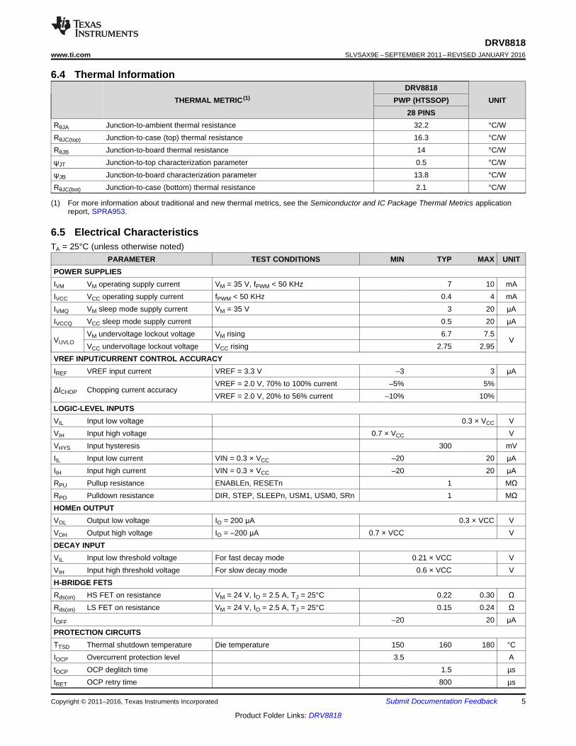
6.4 Thermal Information
THERMAL METRIC (1)DRV8818
UNITPWP (HTSSOP)28 PINS
RθJA Junction-to-ambient thermal resistance 32.2 °C/WRθJC(top) Junction-to-case (top) thermal resistance 16.3 °C/WRθJB Junction-to-board thermal resistance 14 °C/WψJT Junction-to-top characterization parameter 0.5 °C/WψJB Junction-to-board characterization parameter 13.8 °C/WRθJC(bot) Junction-to-case (bottom) thermal resistance 2.1 °C/W
6.5 Electrical CharacteristicsTA = 25°C (unless otherwise noted)
PARAMETER TEST CONDITIONS MIN TYP MAX UNITPOWER SUPPLIESIVM VM operating supply current VM = 35 V, fPWM < 50 KHz 7 10 mAIVCC VCC operating supply current fPWM < 50 KHz 0.4 4 mAIVMQ VM sleep mode supply current VM = 35 V 3 20 μAIVCCQ VCC sleep mode supply current 0.5 20 μA
VUVLOVM undervoltage lockout voltage VM rising 6.7 7.5
VVCC undervoltage lockout voltage VCC rising 2.75 2.95
VREF INPUT/CURRENT CONTROL ACCURACYIREF VREF input current VREF = 3.3 V –3 3 μA
ΔICHOP Chopping current accuracyVREF = 2.0 V, 70% to 100% current –5% 5%VREF = 2.0 V, 20% to 56% current –10% 10%
LOGIC-LEVEL INPUTSVIL Input low voltage 0.3 × VCC VVIH Input high voltage 0.7 × VCC VVHYS Input hysteresis 300 mVIIL Input low current VIN = 0.3 × VCC –20 20 μAIIH Input high current VIN = 0.3 × VCC –20 20 μARPU Pullup resistance ENABLEn, RESETn 1 MΩRPD Pulldown resistance DIR, STEP, SLEEPn, USM1, USM0, SRn 1 MΩHOMEn OUTPUTVOL Output low voltage IO = 200 μA 0.3 × VCC VVOH Output high voltage IO = –200 μA 0.7 × VCC VDECAY INPUTVIL Input low threshold voltage For fast decay mode 0.21 × VCC VVIH Input high threshold voltage For slow decay mode 0.6 × VCC VH-BRIDGE FETSRds(on) HS FET on resistance VM = 24 V, IO = 2.5 A, TJ = 25°C 0.22 0.30 ΩRds(on) LS FET on resistance VM = 24 V, IO = 2.5 A, TJ = 25°C 0.15 0.24 ΩIOFF –20 20 μAPROTECTION CIRCUITSTTSD Thermal shutdown temperature Die temperature 150 160 180 °CIOCP Overcurrent protection level 3.5 AtOCP OCP deglitch time 1.5 µstRET OCP retry time 800 µs
STEP
DIR, USMx
SLEEPn, ENABLEn, RESETn
1
2 3
4 5
6
OUTPUT
8
10
7
9
11
6
DRV8818SLVSAX9E –SEPTEMBER 2011–REVISED JANUARY 2016 www.ti.com
Product Folder Links: DRV8818
Submit Documentation Feedback Copyright © 2011–2016, Texas Instruments Incorporated
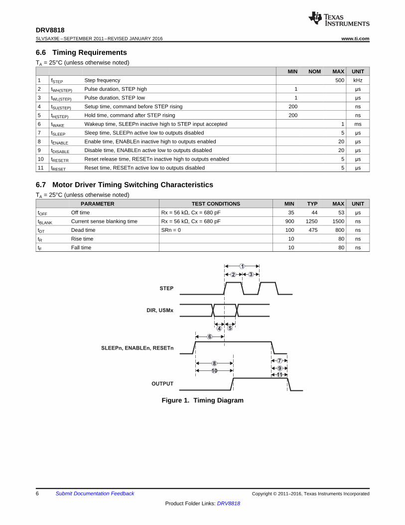
6.6 Timing RequirementsTA = 25°C (unless otherwise noted)
MIN NOM MAX UNIT1 fSTEP Step frequency 500 kHz2 tWH(STEP) Pulse duration, STEP high 1 μs3 tWL(STEP) Pulse duration, STEP low 1 μs4 tSU(STEP) Setup time, command before STEP rising 200 ns5 tH(STEP) Hold time, command after STEP rising 200 ns6 tWAKE Wakeup time, SLEEPn inactive high to STEP input accepted 1 ms7 tSLEEP Sleep time, SLEEPn active low to outputs disabled 5 μs8 tENABLE Enable time, ENABLEn inactive high to outputs enabled 20 μs9 tDISABLE Disable time, ENABLEn active low to outputs disabled 20 μs10 tRESETR Reset release time, RESETn inactive high to outputs enabled 5 μs11 tRESET Reset time, RESETn active low to outputs disabled 5 μs
6.7 Motor Driver Timing Switching CharacteristicsTA = 25°C (unless otherwise noted)
PARAMETER TEST CONDITIONS MIN TYP MAX UNITtOFF Off time Rx = 56 kΩ, Cx = 680 pF 35 44 53 μstBLANK Current sense blanking time Rx = 56 kΩ, Cx = 680 pF 900 1250 1500 nstDT Dead time SRn = 0 100 475 800 nstR Rise time 10 80 nstF Fall time 10 80 ns
Figure 1. Timing Diagram

Temperature (qC)
RD
S(o
n) H
S +
LS
(m:
)
-40 -20 0 20 40 60 80 100270
300
330
360
390
420
450
480
510
D003
8 V24 V35 V
VM (V)
RD
S(o
n) H
S
LS
(m:
)
6 9 12 15 18 21 24 27 30 33 36275
300
325
350
375
400
425
450
475
500
525
D004
±qC25qC85qC
Temperature (qC)
I VM
(m
A)
-40 -20 0 20 40 60 80 1004
4.5
5
5.5
6
6.5
7
7.5
D001
8 V24 V35 V
Temperature (qC)
I VM
Q (P
A)
-40 -20 0 20 40 60 80 1000
1
2
3
4
5
6
D002
8 V24 V35 V
7
DRV8818www.ti.com SLVSAX9E –SEPTEMBER 2011–REVISED JANUARY 2016
Product Folder Links: DRV8818
Submit Documentation FeedbackCopyright © 2011–2016, Texas Instruments Incorporated
6.8 Typical Characteristics
Figure 2. IVM vs Temperature Figure 3. IVMQ vs Temperature
Figure 4. RDS(ON) HS + LS vs Temperature Figure 5. RDS(ON) HS + LS vs VM

8
DRV8818SLVSAX9E –SEPTEMBER 2011–REVISED JANUARY 2016 www.ti.com
Product Folder Links: DRV8818
Submit Documentation Feedback Copyright © 2011–2016, Texas Instruments Incorporated
7 Detailed Description
7.1 OverviewThe DRV8818 is a highly configurable, integrated motor driver solution for bipolar stepper motors. The deviceintegrates two H-bridges, current sense and regulation circuitry, and a microstepping indexer. The DRV8818 canbe powered with a supply voltage between 8 V and 35 V and is capable of providing an output current up to 2.5A full-scale.
A simple STEP/DIR interface allows for easy interfacing to the controller. The internal indexer is able to executehigh-accuracy microstepping without requiring the controller to manage the current regulation loop.
The current regulation is highly configurable, with three decay modes of operation. They are fast, slow, andmixed decay, which can be selected depending on the application requirements. The DRV8818 also providesconfigurable mixed decay, blanking, and off time in order to adjust to a wide range of motors.
A low-power sleep mode is incorporated which allows for minimal power consumption when the system is idle.

GND GNDPPAD
HOMEn
SRn
RESETn
USM1
USM0
DIR
SLEEPn
RESETn
ENABLEn
Control Logic/
Indexer
STEP
Internal Logic Regulator and
References
Low Side Gate Drive
VREF
VCC
VCC
VCC
Thermal Shut Down
Motor Driver B
Motor Driver A
Charge Pump
ISENB
BOUT2
BOUT1
VMB
ISENA
AOUT2
AOUT1
VMA
VCP
CP2
CP1
VM
VMHS Gate
Drive
LS Gate Drive
VM
VM
+
+ -
-
Stepper Motor
+
VGD
VM
LS Gate Drive
DECAY
VCC
RCA
RCB
9
DRV8818www.ti.com SLVSAX9E –SEPTEMBER 2011–REVISED JANUARY 2016
Product Folder Links: DRV8818
Submit Documentation FeedbackCopyright © 2011–2016, Texas Instruments Incorporated
7.2 Functional Block Diagram
AOUT1
AOUT2
BOUT1
BOUT2
StepMotor
VMA
VMB
ISENA
ISENB
VREF
Pre-
drive
Pre-
drive
VCP
VM
VM
+
-
PWM
VCP
+
-
PWM
DAC
DAC
A=8
A=8
Control / Indexer
Logic
DECAY
RCB
RCA
VGD
VGD
+
+ -
-
10
DRV8818SLVSAX9E –SEPTEMBER 2011–REVISED JANUARY 2016 www.ti.com
Product Folder Links: DRV8818
Submit Documentation Feedback Copyright © 2011–2016, Texas Instruments Incorporated
7.3 Feature Description
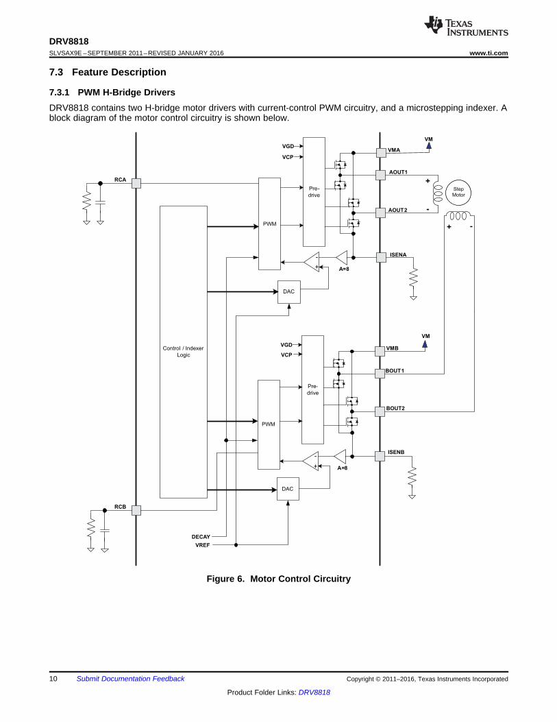
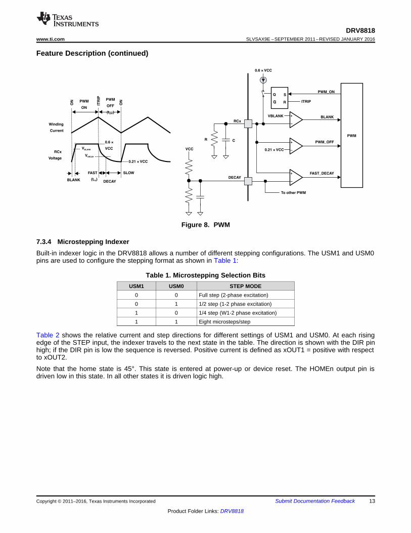
7.3.1 PWM H-Bridge DriversDRV8818 contains two H-bridge motor drivers with current-control PWM circuitry, and a microstepping indexer. Ablock diagram of the motor control circuitry is shown below.
Figure 6. Motor Control Circuitry

1400BLANK
t C= ·
OFFt R C= ·
8
REFX
CHOP
ISENSE
VI
R=
·
11
DRV8818www.ti.com SLVSAX9E –SEPTEMBER 2011–REVISED JANUARY 2016
Product Folder Links: DRV8818
Submit Documentation FeedbackCopyright © 2011–2016, Texas Instruments Incorporated
Feature Description (continued)7.3.2 Current RegulationThe PWM chopping current is set by a comparator, which compares the voltage across a current sense resistor,multiplied by a factor of 8, with a reference voltage. The reference voltage is input from the VREF pin. The full-scale (100%) chopping current is calculated as follows:
(1)
Example:
If a 0.22-Ω sense resistor is used and the VREFx pin is 3.3 V, the full-scale (100%) chopping current is3.3 V / (8 × 0.22 Ω) = 1.875 A.
The reference voltage is also scaled by an internal DAC that allows torque control for fractional stepping of abipolar stepper motor, as described in the Microstepping Indexer section.
When a winding is activated, the current through it rises until it reaches the chopping current threshold describedabove, then the current is switched off for a fixed off time. The off time is determined by the values of a resistorand capacitor connected to the RCA (for bridge A) and RCB (for bridge B) pins. The off time is approximated by:
(2)
To avoid falsely tripping on transient currents when the winding is first activated, a blanking period is usedimmediately after turning on the FETs, during which the state of the current sense comparator is ignored. Theblanking time is determined by the value of the capacitor connected to the RCx pin and is approximated by:
(3)
7.3.3 Decay ModeDuring PWM current chopping, the H-bridge is enabled to drive through the motor winding until the PWM currentchopping threshold is reached. This is shown in Figure 7, Item 1. The current flow direction shown indicatespositive current flow in the step table below.
Once the chopping current threshold is reached, the H-bridge can operate in two different states, fast decay orslow decay.
In fast decay mode, once the PWM chopping current level has been reached, the H-bridge reverses state toallow winding current to flow in a reverse direction. If synchronous rectification is enabled (SRn pin logic low), theopposite FETs are turned on; as the winding current approaches zero, the bridge is disabled to prevent anyreverse current flow. If SRn is high, current is recirculated through the body diodes, or through external Schottkydiodes. Fast-decay mode is shown in Figure 7, Item 2.
In slow-decay mode, winding current is re-circulated by enabling both of the low-side FETs in the bridge. This isshown in Figure 7, Item 3.
If SRn is high, current is recirculated only through the body diodes, or through external Schottky diodes. In thiscase fast decay is always used.

0.6CC
FD
DECAY
Vt R C In
V
æ ö·= · · ç ÷è ø
xOUT1 xOUT2
3
1
2
3
Drive current
Slow decay (brake)
Fast decay (reverse)
VM
1
2
12
DRV8818SLVSAX9E –SEPTEMBER 2011–REVISED JANUARY 2016 www.ti.com
Product Folder Links: DRV8818
Submit Documentation Feedback Copyright © 2011–2016, Texas Instruments Incorporated
Feature Description (continued)
Figure 7. Decay Mode
The DRV8818 also supports a mixed decay mode. Mixed decay mode begins as fast decay, but after a period oftime switches to slow decay mode for the remainder of the fixed off time.
Fast and mixed decay modes are only active if the current through the winding is decreasing; if the current isincreasing, then slow decay is always used.
Which decay mode is used is selected by the voltage on the DECAY pin. If the voltage is greater than 0.6 × VCC,slow decay mode is always used. If DECAY is less than 0.21 × VCC, the device operates in fast decay modewhen the current through the winding is decreasing. If the voltage is between these levels, mixed decay mode isenabled.
In mixed decay mode, the voltage on the DECAY pin sets the point in the cycle that the change to slow decaymode occurs. This time can be approximated by:
(4)
Mixed decay mode is only used while the current though the winding is decreasing; slow decay is used while thecurrent is increasing.
Operation of the blanking, fixed off time, and mixed decay mode is illustrated in Figure 8.
PWM
RCx
PWM_ON
DECAY
VCC
BLANK
PWM_OFF
VBLANK
SQ
Q R
FAST_DECAY
0.21 × VCC
CR
BLANK
ON
ITR
IP
ONPWM
ON
PWM
OFF
(tOFF)
Winding
Current
RCx
Voltage
ITRIP
0.6 × VCC
0.6 ×
VCC
0.21 × VCC
To other PWM
VDECAY
FAST
(tFD)
SLOW
DECAY
VBLANK
13
DRV8818www.ti.com SLVSAX9E –SEPTEMBER 2011–REVISED JANUARY 2016
Product Folder Links: DRV8818
Submit Documentation FeedbackCopyright © 2011–2016, Texas Instruments Incorporated
Feature Description (continued)
Figure 8. PWM
7.3.4 Microstepping IndexerBuilt-in indexer logic in the DRV8818 allows a number of different stepping configurations. The USM1 and USM0pins are used to configure the stepping format as shown in Table 1:
Table 1. Microstepping Selection BitsUSM1 USM0 STEP MODE
0 0 Full step (2-phase excitation)0 1 1/2 step (1-2 phase excitation)1 0 1/4 step (W1-2 phase excitation)1 1 Eight microsteps/step
Table 2 shows the relative current and step directions for different settings of USM1 and USM0. At each risingedge of the STEP input, the indexer travels to the next state in the table. The direction is shown with the DIR pinhigh; if the DIR pin is low the sequence is reversed. Positive current is defined as xOUT1 = positive with respectto xOUT2.
Note that the home state is 45°. This state is entered at power-up or device reset. The HOMEn output pin isdriven low in this state. In all other states it is driven logic high.

14
DRV8818SLVSAX9E –SEPTEMBER 2011–REVISED JANUARY 2016 www.ti.com
Product Folder Links: DRV8818
Submit Documentation Feedback Copyright © 2011–2016, Texas Instruments Incorporated
Table 2. Microstepping Indexer
FULL STEPUSM = 00
1/2 STEPUSM = 01
1/4 STEPUSM = 10
1/8 STEPUSM = 11
AOUTxCURRENT
(% FULL-SCALE)
BOUTxCURRENT
(% FULL-SCALE)STEP ANGLE
(°)
1 1 1 100 0 02 98 20 11.325
2 3 92 38 22.54 83 56 33.75
1 2 3 5 71 71 45 (home state)6 56 83 56.25
4 7 38 92 67.58 20 98 78.75
3 5 9 0 100 9010 –20 98 101.25
6 11 –38 92 112.512 –56 83 123.75
2 4 7 13 –71 71 13514 –83 56 146.25
8 15 –92 38 157.516 –98 20 168.75
5 9 17 –100 0 18018 –98 –20 191.25
10 19 –92 –38 202.520 –83 –56 213.75
3 6 11 21 –71 –71 22522 –56 –83 236.25
12 23 –38 –92 247.524 –20 –98 258.75
7 13 25 0 –100 27026 20 –98 281.25
14 27 38 –92 292.528 56 –83 303.75
4 8 15 29 71 –71 31530 83 –56 326.25
16 31 92 –38 337.532 98 –20 348.75
7.3.5 Protection Circuits
7.3.5.1 Overcurrent Protection (OCP)If the current through any FET exceeds the preset overcurrent threshold, all FETs in the H-bridge will be disabledfor a period of approximately 800 µs, or until the ENABLEn pin has been brought inactive high and then backlow, or power is removed and reapplied. Overcurrent conditions are sensed in both directions; that is, a short toground, supply, or across the motor winding will all result in an overcurrent shutdown.
Note that overcurrent protection does not use the current sense circuitry used for PWM current control and isindependent of the Isense resistor value or VREF voltage. Additionally, in the case of an overcurrent event, themicrostepping indexer will be reset to the home state.
7.3.5.2 Thermal Shutdown (TSD)If the die temperature exceeds safe limits, all drivers in the device are shut down and the indexer is reset to thehome state. Once the die temperature has fallen to a safe level operation resumes.
15
DRV8818www.ti.com SLVSAX9E –SEPTEMBER 2011–REVISED JANUARY 2016
Product Folder Links: DRV8818
Submit Documentation FeedbackCopyright © 2011–2016, Texas Instruments Incorporated
7.3.5.3 Undervoltage Lockout (UVLO)If at any time the voltage on the VM or VCC pins falls below the VM or VCC undervoltage lockout thresholdvoltage, all circuitry in the device will be disabled, and the indexer will be reset to the home state. Operation willresume when VM and VCC both rise above their UVLO thresholds.
7.4 Device Functional Modes
7.4.1 RESETn, ENABLEn, and SLEEPn OperationThe RESETn pin, when driven active low, resets the step table to the home position. It also disables the H-bridgedrivers. The STEP input is ignored while RESETn is active.
The ENABLEn pin is used to control the output drivers. When ENABLEn is low, the output H-bridges areenabled. When ENABLEn is high, the H-bridges are disabled and the outputs are in a high-impedance state.
Note that when ENABLEn is high, the input pins and control logic, including the indexer (STEP and DIR pins) arestill functional.
The SLEEPn pin is used to put the device into a low power state. If SLEEPn is low, the H-bridges are disabled,the gate drive charge pump is stopped, and all internal clocks are stopped. In this state all inputs are ignoreduntil the SLEEPn pin returns high.
7.4.2 Decay ModesThe DRV8818 supports three different decay modes: slow decay, fast decay, and mixed decay. The currentthrough the motor windings is regulated using a fixed off time scheme.
This means that the current will increase until it reaches the current chopping threshold (ITRIP), after which it willenter the set decay mode for a fixed period of time. The cycle will then repeat after the decay period expires.
The blanking time tBLANK defines the minimum drive time for the current chopping. ITRIP is ignored during tBLANK,so the winding current may overshoot the trip level.
VMA
SLEEPn
ENABLEn
AOUT2
CP2
CP1
VCP
GND
VGD
STEP
BOUT2
RESETn
SRn
VMB
ISENA
HOMEn
DIR
AOUT1
DECAY
RCA
GND
VREF
RCB
VCC
BOUT1
USM1
USM0
ISENB
DRV8818P
PA
D
0.22 µF
100 m
100 m
+ ±
Stepper Motor
+±
100 uF
VM
+
VM
VCC
10 k
10 k
1
2
3
4
5
6
7
8
9
10
11
12
13
14 15
16
17
18
19
20
21
22
23
24
25
26
27
28
0.1 µF
BOUT1
47 k
1000 pF
47 k
1000 pF
VCC
VCC
10 k
10 k
BOUT2
AOUT2
0.22 µF
0.22 µF
VM
0.1 µF
VM
0.1 µF
BO
UT
2
AOUT2
AOUT1
BO
UT
1
AOUT1
16
DRV8818SLVSAX9E –SEPTEMBER 2011–REVISED JANUARY 2016 www.ti.com
Product Folder Links: DRV8818
Submit Documentation Feedback Copyright © 2011–2016, Texas Instruments Incorporated
8 Application and Implementation
NOTEInformation in the following applications sections is not part of the TI componentspecification, and TI does not warrant its accuracy or completeness. TI’s customers areresponsible for determining suitability of components for their purposes. Customers shouldvalidate and test their design implementation to confirm system functionality.
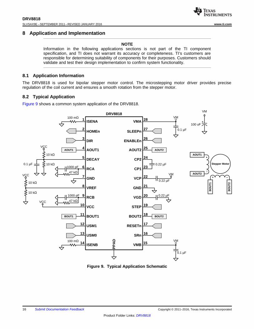
8.1 Application InformationThe DRV8818 is used for bipolar stepper motor control. The microstepping motor driver provides preciseregulation of the coil current and ensures a smooth rotation from the stepper motor.
8.2 Typical ApplicationFigure 9 shows a common system application of the DRV8818.
Figure 9. Typical Application Schematic
8 FS
v SENSE SENSE
VREF V VREF VI A
A x R x Rß ß
120 360 8
/
60 1.8
§ ·q§ · § ·u u¨ ¸ ¨ ¸ ¨ ¸© ¹ © ¹ © ¹
§ ·q§ · u¨ ¸ ¨ ¸© ¹ © ¹
step
rotations µsteps
minute rotation stepf µsteps second
seconds
minute step
step
360
/
60
§ ·q§ · § ·u u¨ ¸ ¨ ¸ ¨ ¸© ¹ © ¹ © ¹
§ ·q§ ·u¨ ¸ ¨ ¸© ¹ © ¹
m
step
rotations µstepsv n
minute rotation stepf µsteps second
seconds
minute step
17
DRV8818www.ti.com SLVSAX9E –SEPTEMBER 2011–REVISED JANUARY 2016
Product Folder Links: DRV8818
Submit Documentation FeedbackCopyright © 2011–2016, Texas Instruments Incorporated
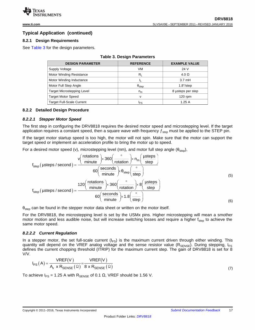
Typical Application (continued)8.2.1 Design RequirementsSee Table 3 for the design parameters.
Table 3. Design ParametersDESIGN PARAMETER REFERENCE EXAMPLE VALUE
Supply Voltage VM 24 VMotor Winding Resistance RL 4.0 ΩMotor Winding Inductance IL 3.7 mHMotor Full Step Angle θstep 1.8°/stepTarget Microstepping Level nm 8 µsteps per stepTarget Motor Speed v 120 rpmTarget Full-Scale Current IFS 1.25 A
8.2.2 Detailed Design Procedure
8.2.2.1 Stepper Motor SpeedThe first step in configuring the DRV8818 requires the desired motor speed and microstepping level. If the targetapplication requires a constant speed, then a square wave with frequency ƒstep must be applied to the STEP pin.
If the target motor startup speed is too high, the motor will not spin. Make sure that the motor can support thetarget speed or implement an acceleration profile to bring the motor up to speed.
For a desired motor speed (v), microstepping level (nm), and motor full step angle (θstep),
(5)
(6)
θstep can be found in the stepper motor data sheet or written on the motor itself.
For the DRV8818, the microstepping level is set by the USMx pins. Higher microstepping will mean a smothermotor motion and less audible noise, but will increase switching losses and require a higher fstep to achieve thesame motor speed.
8.2.2.2 Current RegulationIn a stepper motor, the set full-scale current (IFS) is the maximum current driven through either winding. Thisquantity will depend on the VREF analog voltage and the sense resistor value (RSENSE). During stepping, IFSdefines the current chopping threshold (ITRIP) for the maximum current step. The gain of DRV8818 is set for 8V/V.
(7)
To achieve IFS = 1.25 A with RSENSE of 0.1 Ω, VREF should be 1.56 V.

18
DRV8818SLVSAX9E –SEPTEMBER 2011–REVISED JANUARY 2016 www.ti.com
Product Folder Links: DRV8818
Submit Documentation Feedback Copyright © 2011–2016, Texas Instruments Incorporated
8.2.3 Application Curves
Figure 10. Mixed Decay Figure 11. Slow Decay on Increasing Steps
Figure 12. Mixed Decay on Decreasing Steps

Local
Bulk Capacitor
Parasitic Wire
Inductance
+–
Motor
Driver
Power Supply Motor Drive System
VM
GND
+
IC Bypass
Capacitor
19
DRV8818www.ti.com SLVSAX9E –SEPTEMBER 2011–REVISED JANUARY 2016
Product Folder Links: DRV8818
Submit Documentation FeedbackCopyright © 2011–2016, Texas Instruments Incorporated
9 Power Supply Recommendations
9.1 Bulk CapacitanceHaving an appropriate local bulk capacitance is an important factor in motor drive system design. It is generallybeneficial to have more bulk capacitance, while the disadvantages are increased cost and physical size.
The amount of local capacitance needed depends on a variety of factors, including:• The highest current required by the motor system• The power supply’s capacitance and ability to source current• The amount of parasitic inductance between the power supply and motor system• The acceptable voltage ripple• The type of motor used (brushed DC, brushless DC, stepper)• The motor braking method
The inductance between the power supply and the motor drive system limits the rate current can change fromthe power supply. If the local bulk capacitance is too small, the system responds to excessive current demandsor dumps from the motor with a change in voltage. When adequate bulk capacitance is used, the motor voltageremains stable and high current can be quickly supplied.
The data sheet generally provides a recommended value, but system-level testing is required to determine theappropriate sized bulk capacitor.
Figure 13. Example Setup of Motor Drive System With External Power Supply
The voltage rating for bulk capacitors should be higher than the operating voltage, to provide margin for caseswhen the motor transfers energy to the supply.
20
DRV8818SLVSAX9E –SEPTEMBER 2011–REVISED JANUARY 2016 www.ti.com
Product Folder Links: DRV8818
Submit Documentation Feedback Copyright © 2011–2016, Texas Instruments Incorporated
10 Layout
10.1 Layout GuidelinesThe VMA and VMB pins should be bypassed to GND using low-ESR ceramic bypass capacitors with arecommended value of 0.1μF rated for VM. This capacitor should be placed as close to the VMA and VMB pinsas possible with a thick trace or ground plane connection to the device GND pin.
The VMA and VMB pins must be bypassed to ground using an appropriate bulk capacitor. This component maybe an electrolytic and should be located close to the DRV8818.
A low-ESR ceramic capacitor must be placed in between the CP1 and CP2 pins. TI recommends a value of0.22-μF rated for VM. Place this component as close to the pins as possible.
A low-ESR ceramic capacitor must be placed in between the VM and VCP pins. TI recommends a value of0.22-μF rated for 16 V. Place this component as close to the pins as possible.
Ensure proper connection of the DRV8818 PowerPAD to the PCB. The PowerPAD should be connected to acopper plane that is connected to GND. The copper plane should have a large area to allow for thermaldissipation from the DRV8818.
10.1.1 HeatsinkingThe PowerPAD™ package uses an exposed pad to remove heat from the device. For proper operation, this padmust be thermally connected to copper on the PCB to dissipate heat. On a multi-layer PCB with a ground plane,this can be accomplished by adding a number of vias to connect the thermal pad to the ground plane. On PCBswithout internal planes, copper area can be added on either side of the PCB to dissipate heat. If the copper areais on the opposite side of the PCB from the device, thermal vias are used to transfer the heat between top andbottom layers.
For details about how to design the PCB, refer to TI Application Report SLMA002, PowerPAD™ ThermallyEnhanced Package and TI Application Brief SLMA004, PowerPAD™ Made Easy, available at www.ti.com.
In general, the more copper area that can be provided, the more power can be dissipated.

P = 4 R (I )TOT DS(ON) OUT(RMS)· ·2
0.22 µF
0.22 µF
ISENA VMA
HOMEn
DIR
AOUT1
DECAY
RCA
GND
VREF
RCB
VCC
BOUT1
USM1
SLEEPn
ENABLE
AOUT2
CP2
CP1
VCP
GND
VGD
STEP
BOUT2
RESETn
USM0
ISENB
SRn
VMB
+100 P
0.22 µF
VCC
VM
VM
GND
GND
GND
GND
GND
100 P
0.1 µF
0.1 µF
21
DRV8818www.ti.com SLVSAX9E –SEPTEMBER 2011–REVISED JANUARY 2016
Product Folder Links: DRV8818
Submit Documentation FeedbackCopyright © 2011–2016, Texas Instruments Incorporated
10.2 Layout Example
Figure 14. Layout Example Schematic
10.3 Thermal ConsiderationsThe DRV8818 has thermal shutdown (TSD) as described previously. If the die temperature exceedsapproximately 150°C, the device will be disabled until the temperature drops to a safe level.
Any tendency of the device to enter thermal shutdown is an indication of either excessive power dissipation,insufficient heatsinking, or too high an ambient temperature.
10.3.1 Power DissipationPower dissipation in the DRV8818 is dominated by the power dissipated in the output FET resistance, or RDS(ON).Average power dissipation when running a stepper motor can be roughly estimated by:
where• PTOT is the total power dissipation.• RDS(ON) is the resistance of each FET.• IOUT(RMS) is the RMS output current being applied to each winding. (8)
22
DRV8818SLVSAX9E –SEPTEMBER 2011–REVISED JANUARY 2016 www.ti.com
Product Folder Links: DRV8818
Submit Documentation Feedback Copyright © 2011–2016, Texas Instruments Incorporated
Thermal Considerations (continued)IOUT(RMS) is equal to the approximately 0.7x the full-scale output current setting. The factor of 4 comes from thefact that there are two motor windings, and at any instant two FETs are conducting winding current for eachwinding (one high-side and one low-side).
The maximum amount of power that can be dissipated in the DRV8818 is dependent on ambient temperatureand heatsinking. The thermal dissipation ratings table in the datasheet can be used to estimate the temperaturerise for typical PCB constructions.
Note that RDS(ON) increases with temperature, so as the device heats, the power dissipation increases. This mustbe taken into consideration when sizing the heatsink.

23
DRV8818www.ti.com SLVSAX9E –SEPTEMBER 2011–REVISED JANUARY 2016
Product Folder Links: DRV8818
Submit Documentation FeedbackCopyright © 2011–2016, Texas Instruments Incorporated
11 Device and Documentation Support
11.1 Documentation Support
11.1.1 Related Documentation1. PowerPAD™ Thermally Enhanced Package, SLMA0022. PowerPAD™ Made Easy, SLMA0043. Current Recirculation and Decay Modes, SLVA3214. Calculating Motor Driver Power Dissipation, SLVA5045. Understanding Motor Driver Current Ratings, SLVA505
11.2 Community ResourcesThe following links connect to TI community resources. Linked contents are provided "AS IS" by the respectivecontributors. They do not constitute TI specifications and do not necessarily reflect TI's views; see TI's Terms ofUse.
TI E2E™ Online Community TI's Engineer-to-Engineer (E2E) Community. Created to foster collaborationamong engineers. At e2e.ti.com, you can ask questions, share knowledge, explore ideas and helpsolve problems with fellow engineers.
Design Support TI's Design Support Quickly find helpful E2E forums along with design support tools andcontact information for technical support.
11.3 TrademarksPowerPAD, E2E are trademarks of Texas Instruments.All other trademarks are the property of their respective owners.
11.4 Electrostatic Discharge CautionThese devices have limited built-in ESD protection. The leads should be shorted together or the device placed in conductive foamduring storage or handling to prevent electrostatic damage to the MOS gates.
11.5 GlossarySLYZ022 — TI Glossary.
This glossary lists and explains terms, acronyms, and definitions.
12 Mechanical, Packaging, and Orderable InformationThe following pages include mechanical, packaging, and orderable information. This information is the mostcurrent data available for the designated devices. This data is subject to change without notice and revision ofthis document. For browser-based versions of this data sheet, refer to the left-hand navigation.

PACKAGE OPTION ADDENDUM
www.ti.com 9-Jul-2014
Addendum-Page 1
PACKAGING INFORMATION
Orderable Device Status(1)
Package Type PackageDrawing
Pins PackageQty
Eco Plan(2)
Lead/Ball Finish(6)
MSL Peak Temp(3)
Op Temp (°C) Device Marking(4/5)
Samples
DRV8818PWP ACTIVE HTSSOP PWP 28 50 Green (RoHS& no Sb/Br)
CU NIPDAU Level-3-260C-168 HR -40 to 85 DRV8818
DRV8818PWPR ACTIVE HTSSOP PWP 28 2000 Green (RoHS& no Sb/Br)
CU NIPDAU Level-3-260C-168 HR -40 to 85 DRV8818
(1) The marketing status values are defined as follows:ACTIVE: Product device recommended for new designs.LIFEBUY: TI has announced that the device will be discontinued, and a lifetime-buy period is in effect.NRND: Not recommended for new designs. Device is in production to support existing customers, but TI does not recommend using this part in a new design.PREVIEW: Device has been announced but is not in production. Samples may or may not be available.OBSOLETE: TI has discontinued the production of the device.
(2) Eco Plan - The planned eco-friendly classification: Pb-Free (RoHS), Pb-Free (RoHS Exempt), or Green (RoHS & no Sb/Br) - please check http://www.ti.com/productcontent for the latest availabilityinformation and additional product content details.TBD: The Pb-Free/Green conversion plan has not been defined.Pb-Free (RoHS): TI's terms "Lead-Free" or "Pb-Free" mean semiconductor products that are compatible with the current RoHS requirements for all 6 substances, including the requirement thatlead not exceed 0.1% by weight in homogeneous materials. Where designed to be soldered at high temperatures, TI Pb-Free products are suitable for use in specified lead-free processes.Pb-Free (RoHS Exempt): This component has a RoHS exemption for either 1) lead-based flip-chip solder bumps used between the die and package, or 2) lead-based die adhesive used betweenthe die and leadframe. The component is otherwise considered Pb-Free (RoHS compatible) as defined above.Green (RoHS & no Sb/Br): TI defines "Green" to mean Pb-Free (RoHS compatible), and free of Bromine (Br) and Antimony (Sb) based flame retardants (Br or Sb do not exceed 0.1% by weightin homogeneous material)
(3) MSL, Peak Temp. - The Moisture Sensitivity Level rating according to the JEDEC industry standard classifications, and peak solder temperature.
(4) There may be additional marking, which relates to the logo, the lot trace code information, or the environmental category on the device.
(5) Multiple Device Markings will be inside parentheses. Only one Device Marking contained in parentheses and separated by a "~" will appear on a device. If a line is indented then it is a continuationof the previous line and the two combined represent the entire Device Marking for that device.
(6) Lead/Ball Finish - Orderable Devices may have multiple material finish options. Finish options are separated by a vertical ruled line. Lead/Ball Finish values may wrap to two lines if the finishvalue exceeds the maximum column width.
Important Information and Disclaimer:The information provided on this page represents TI's knowledge and belief as of the date that it is provided. TI bases its knowledge and belief on informationprovided by third parties, and makes no representation or warranty as to the accuracy of such information. Efforts are underway to better integrate information from third parties. TI has taken andcontinues to take reasonable steps to provide representative and accurate information but may not have conducted destructive testing or chemical analysis on incoming materials and chemicals.TI and TI suppliers consider certain information to be proprietary, and thus CAS numbers and other limited information may not be available for release.
PACKAGE OPTION ADDENDUM
www.ti.com 9-Jul-2014
Addendum-Page 2
In no event shall TI's liability arising out of such information exceed the total purchase price of the TI part(s) at issue in this document sold by TI to Customer on an annual basis.
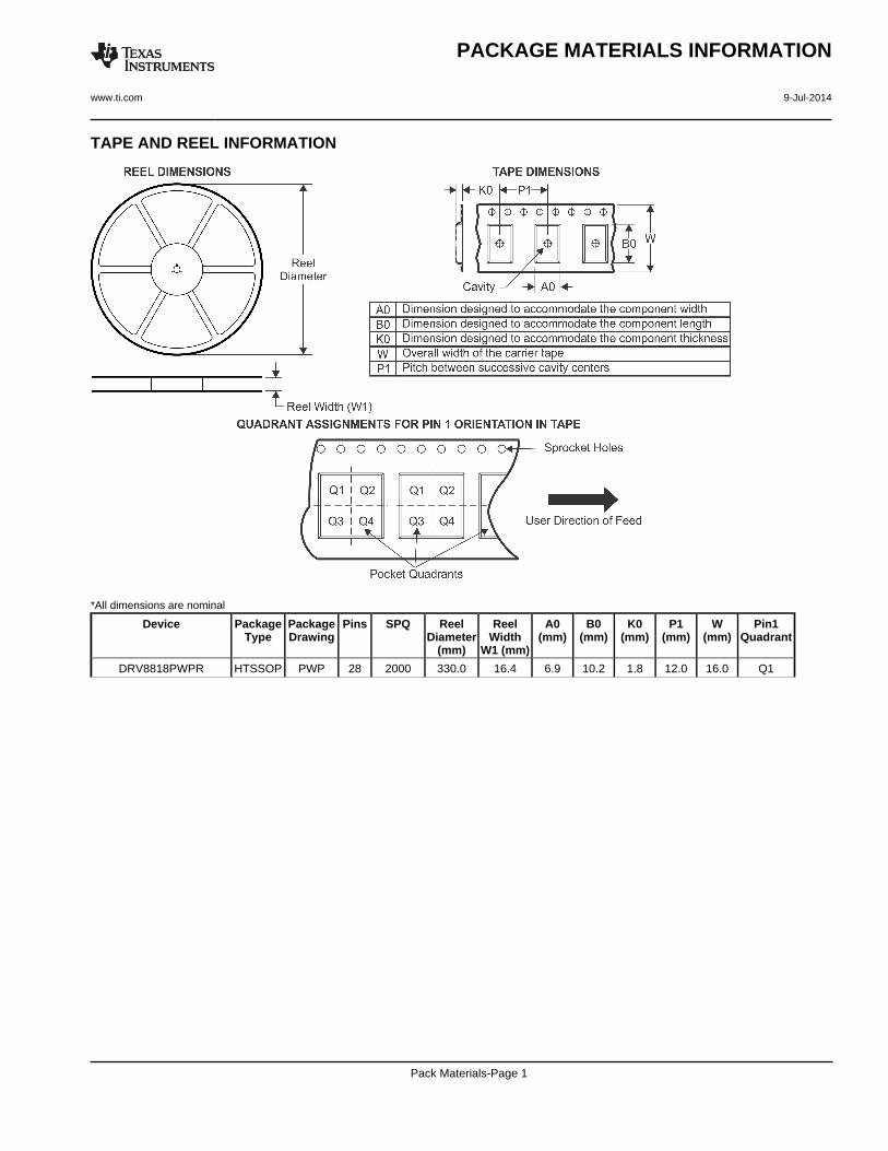
TAPE AND REEL INFORMATION
*All dimensions are nominal
Device PackageType
PackageDrawing
Pins SPQ ReelDiameter
(mm)
ReelWidth
W1 (mm)
A0(mm)
B0(mm)
K0(mm)
P1(mm)
W(mm)
Pin1Quadrant
DRV8818PWPR HTSSOP PWP 28 2000 330.0 16.4 6.9 10.2 1.8 12.0 16.0 Q1
PACKAGE MATERIALS INFORMATION
www.ti.com 9-Jul-2014
Pack Materials-Page 1

*All dimensions are nominal
Device Package Type Package Drawing Pins SPQ Length (mm) Width (mm) Height (mm)
DRV8818PWPR HTSSOP PWP 28 2000 367.0 367.0 38.0
PACKAGE MATERIALS INFORMATION
www.ti.com 9-Jul-2014
Pack Materials-Page 2
IMPORTANT NOTICE
Texas Instruments Incorporated and its subsidiaries (TI) reserve the right to make corrections, enhancements, improvements and otherchanges to its semiconductor products and services per JESD46, latest issue, and to discontinue any product or service per JESD48, latestissue. Buyers should obtain the latest relevant information before placing orders and should verify that such information is current andcomplete. All semiconductor products (also referred to herein as “components”) are sold subject to TI’s terms and conditions of salesupplied at the time of order acknowledgment.TI warrants performance of its components to the specifications applicable at the time of sale, in accordance with the warranty in TI’s termsand conditions of sale of semiconductor products. Testing and other quality control techniques are used to the extent TI deems necessaryto support this warranty. Except where mandated by applicable law, testing of all parameters of each component is not necessarilyperformed.TI assumes no liability for applications assistance or the design of Buyers’ products. Buyers are responsible for their products andapplications using TI components. To minimize the risks associated with Buyers’ products and applications, Buyers should provideadequate design and operating safeguards.TI does not warrant or represent that any license, either express or implied, is granted under any patent right, copyright, mask work right, orother intellectual property right relating to any combination, machine, or process in which TI components or services are used. Informationpublished by TI regarding third-party products or services does not constitute a license to use such products or services or a warranty orendorsement thereof. Use of such information may require a license from a third party under the patents or other intellectual property of thethird party, or a license from TI under the patents or other intellectual property of TI.Reproduction of significant portions of TI information in TI data books or data sheets is permissible only if reproduction is without alterationand is accompanied by all associated warranties, conditions, limitations, and notices. TI is not responsible or liable for such altereddocumentation. Information of third parties may be subject to additional restrictions.Resale of TI components or services with statements different from or beyond the parameters stated by TI for that component or servicevoids all express and any implied warranties for the associated TI component or service and is an unfair and deceptive business practice.TI is not responsible or liable for any such statements.Buyer acknowledges and agrees that it is solely responsible for compliance with all legal, regulatory and safety-related requirementsconcerning its products, and any use of TI components in its applications, notwithstanding any applications-related information or supportthat may be provided by TI. Buyer represents and agrees that it has all the necessary expertise to create and implement safeguards whichanticipate dangerous consequences of failures, monitor failures and their consequences, lessen the likelihood of failures that might causeharm and take appropriate remedial actions. Buyer will fully indemnify TI and its representatives against any damages arising out of the useof any TI components in safety-critical applications.In some cases, TI components may be promoted specifically to facilitate safety-related applications. With such components, TI’s goal is tohelp enable customers to design and create their own end-product solutions that meet applicable functional safety standards andrequirements. Nonetheless, such components are subject to these terms.No TI components are authorized for use in FDA Class III (or similar life-critical medical equipment) unless authorized officers of the partieshave executed a special agreement specifically governing such use.Only those TI components which TI has specifically designated as military grade or “enhanced plastic” are designed and intended for use inmilitary/aerospace applications or environments. Buyer acknowledges and agrees that any military or aerospace use of TI componentswhich have not been so designated is solely at the Buyer's risk, and that Buyer is solely responsible for compliance with all legal andregulatory requirements in connection with such use.TI has specifically designated certain components as meeting ISO/TS16949 requirements, mainly for automotive use. In any case of use ofnon-designated products, TI will not be responsible for any failure to meet ISO/TS16949.
Products ApplicationsAudio www.ti.com/audio Automotive and Transportation www.ti.com/automotiveAmplifiers amplifier.ti.com Communications and Telecom www.ti.com/communicationsData Converters dataconverter.ti.com Computers and Peripherals www.ti.com/computersDLP® Products www.dlp.com Consumer Electronics www.ti.com/consumer-appsDSP dsp.ti.com Energy and Lighting www.ti.com/energyClocks and Timers www.ti.com/clocks Industrial www.ti.com/industrialInterface interface.ti.com Medical www.ti.com/medicalLogic logic.ti.com Security www.ti.com/securityPower Mgmt power.ti.com Space, Avionics and Defense www.ti.com/space-avionics-defenseMicrocontrollers microcontroller.ti.com Video and Imaging www.ti.com/videoRFID www.ti-rfid.comOMAP Applications Processors www.ti.com/omap TI E2E Community e2e.ti.comWireless Connectivity www.ti.com/wirelessconnectivity
Mailing Address: Texas Instruments, Post Office Box 655303, Dallas, Texas 75265Copyright © 2016, Texas Instruments Incorporated