Draft Standard for a Mixed-Signal Test Bus
123
P1149.4 1 D26 18 May 1999 Copyright © 1999 IEEE. All rights reserved. This is an unapproved IEEE Standard Draft, subject to change. P1149.4/D26 Draft Standard for a Mixed-Signal Test Bus Prepared by the Mixed-Signal Working Group of the Test Technology Technical Committee of the IEEE Computer Society Copyright © 1999 by the Institute of Electrical and Electronics Engineers, Inc. 345 East 47th Street New York, NY 10017, USA All Rights Reserved. This is an IEEE Standards Project, subject to change. Permission is hereby granted for IEEE Standards Committee participants to reproduce this document for purposes of IEEE standardisation activities, including balloting and coordination. If this document is to be submitted to ISO or IEC, notification shall be given to the IEEE Copyrights Administrator. Permission is also granted for member bodies and technical committees of ISO and IEC to reproduce this document for purposes of developing a national position. Other entities seeking permission to reproduce portions of this document for these or other uses must contact the IEEE Standards Department for the appropriate license. Use of information contained in the unapproved draft is at your own risk. IEEE Standards Department Copyrights and Permissions 445 Hoes Lane, PO Box 1331 Piscataway, NJ 08855-1331, USA Abstract : The testability structure for digital circuits described in IEEE Std 1149.1 has been extended to provide similar facilities for mixed-signal circuits. The architecture is described, together with the means of control of and of access to both analog and digital test data. Sample implementation and application details (which are not part of the standard) are included for illustrative purposes. Keywords : analog test, mixed-signal test, boundary-scan, design for testability, board testing, in- circuit test.
Transcript of Draft Standard for a Mixed-Signal Test Bus
P1149.4 1 D26 18 May 1999
Copyright © 1999 IEEE. All rights reserved.This is an unapproved IEEE Standard Draft, subject to change.
P1149.4/D26Draft Standard for a Mixed-Signal Test Bus
Prepared by the Mixed-Signal Working Group of theTest Technology Technical Committee
of the IEEE Computer Society
Copyright © 1999 by the Institute of Electrical and Electronics Engineers, Inc.345 East 47th StreetNew York, NY 10017, USAAll Rights Reserved.
This is an IEEE Standards Project, subject to change. Permission is hereby granted for IEEEStandards Committee participants to reproduce this document for purposes of IEEE standardisationactivities, including balloting and coordination. If this document is to be submitted to ISO or IEC,notification shall be given to the IEEE Copyrights Administrator. Permission is also granted formember bodies and technical committees of ISO and IEC to reproduce this document for purposesof developing a national position. Other entities seeking permission to reproduce portions of thisdocument for these or other uses must contact the IEEE Standards Department for the appropriatelicense. Use of information contained in the unapproved draft is at your own risk.
IEEE Standards DepartmentCopyrights and Permissions445 Hoes Lane, PO Box 1331Piscataway, NJ 08855-1331, USA
Abstract : The testability structure for digital circuits described in IEEE Std 1149.1 has beenextended to provide similar facilities for mixed-signal circuits. The architecture is described, togetherwith the means of control of and of access to both analog and digital test data. Sampleimplementation and application details (which are not part of the standard) are included for illustrativepurposes.
Keywords : analog test, mixed-signal test, boundary-scan, design for testability, board testing, in-circuit test.

P1149.4 2 D26 18 May 1999
Copyright © 1999 IEEE. All rights reserved.This is an unapproved IEEE Standard Draft, subject to change.
Introduction
(This Introduction is not a part of P1149.4 - Mixed-Signal Test Bus)
The development of this standard began with a preliminary meeting in the summer of 1991, when theneed was recognized for a standardized structure to be incorporated into mixed-signal circuits tocombat the testability problems posed by such circuits. This meeting adopted as its mission
To define, document, and promote the use of a standard mixed-signal test busthat can be used at the device and assembly levels to improve the controllabilityand observability of mixed-signal designs and to support mixed-signal built-intest structures in order to reduce both test development time and testing costs,and to improve test quality.
The work received the support of the Test Technology Technical Committee of the Computer Societyin November 1991, and the Working Group started work under the Chairmanship of Prof. ManiSoma. In January 1995, Professor Soma resigned as chair and Adam Cron was elected chair of theWorking Group.
At the time of issue of this draft, the members of the Working Group were:
Adam Cron, Chair Stephen Sunter, Vice-Chair
Brian Wilkins, Editor Elbert Nhan, Secretary
John Andrews Allen Heiden Adam OsseiranTerry Borroz Katsuhiro Hirayama Kenneth P. ParkerC.J. Clark Terry Junge Adam SheppardBill Coombe Keith Lofstrom Mani Soma, Chair EmeritusRamaswami Dandapani Akira Matsuzawa Anthony J. SutoFrans de Jong John McDermid Lee WhetselTed Eaton
In the development of this Standard, the Working Group was supported by many other individualsfrom many different organizations who contributed time, administrative effort, and technicalsuggestions.

P1149.4 3 D26 18 May 1999
Copyright © 1999 IEEE. All rights reserved.This is an unapproved IEEE Standard Draft, subject to change.
In particular, the working group wishes to acknowledge the contributions made by the followingindividuals:
Jose C. Alves Mehdi Katoozi Luigi Napoli Keith Baker Mike Kondrat Mary Lynne Nielsen Cary Champlin Atsushi Kukutsu Franc Novak Bernard Courtois Robert Labelle Kozo NuriyaCraig Danes Tom Langford Stig OresjoSteven Dollens Ana C. Leao Michel ParotKathy A. Doty Nai Chi Lee Walter PienciakMarie English Adam Ley Robert RussellFirooz Farhoomand Jose Machado da Silva Bill SmithTom Fisher Charles P. Mangan Mick Tegethoff Ren Franse J. Silva Matos Carl ThatcherJoel Goldberg Colin Maunder Mike Topsakal Grady Giles Patrick McHugh Stefan Trost Dick Howell Charles Meyerson Rodham E. TullossJay Iorio Joseph A. Mielke Martin Viktil Madhuri Jarwala Naveena Nagi Thomas E. Wulling
P1149.4 4 D26 18 May 1999
Copyright © 1999 IEEE. All rights reserved.This is an unapproved IEEE Standard Draft, subject to change.
TABLE OF CONTENTS
1 Overview 71.1 Organization of the standard 71.2 Context 71.3 Scope of the standard 9
1.3.1 Aims 91.3.2 Interconnect testing 91.3.3 Parametric Test 101.3.4 Internal test 12
1.4 Background reading 122 References 143 Definitions, acronyms, and voltage symbols 15
3.1 Definitions 153.2 Acronyms 203.3 Voltage source symbols 21
4 Testability Architecture 224.1 Overview 224.2 TAP controller 24
4.2.1 State sequence 244.2.2 Initialization 244.2.3 Controller outputs 25
4.3 Analog test access port (ATAP) 264.4 Register architecture 26
5 Instructions 295.1 General 295.2 Response of test logic to instructions 305.3 Mandatory instructions 31
5.3.1 The BYPASS instruction 315.3.2 The SAMPLE/PRELOAD instruction 325.3.3 The EXTEST instruction 335.3.4 The PROBE instruction 34
5.4 Optional instructions 355.4.1 The INTEST instruction 355.4.2 Device identification register instructions 38
5.4.2.1 The IDCODE instruction 385.4.2.2 The USERCODE instruction 39
P1149.4 5 D26 18 May 1999
Copyright © 1999 IEEE. All rights reserved.This is an unapproved IEEE Standard Draft, subject to change.
5.4.3 The RUNBIST instruction 405.4.4 The CLAMP instruction 415.4.5 The HIGHZ instruction 41
6 The Test Bus Interface Circuit (TBIC) 436.1 General 436.2 Test bus and TBIC structure 436.3 Control of the TBIC 506.4 Differential I/O 556.5 Partitioned internal test bus structure 55
6.5.1 Switching 556.5.2 Control 58
7 The Boundary-Scan Register 607.1 Structure 607.2 Digital boundary modules (DBMs) 61
7.2.1 Specification 617.2.2 Description 63
7.3 Analog boundary modules (ABMs) 647.3.1 Specification 647.3.2 Description 667.3.3 Residual elements 687.3.4 ABM switch patterns 717.3.5 Control of the ABM 75
7.4 Differential analog boundary modules 788 Measurement Methodology 86
8.1 Interconnect testing 868.1.1 Simple interconnect testing 868.1.2 Differential interconnect testing 868.1.3 Differential I/O 88
8.2 Extended interconnect testing 898.2.1 Virtual probing 898.2.2 Extended interconnect measurements 90
8.3 Network measurements 949 Analog parametric limits 96
9.1 General 969.2 Switch limitations 969.3 Electrostatic protection 989.4 Performance specifications 999.5 Measuring performance 102
9.5.1 Delivering a defined current stimulus 102
P1149.4 6 D26 18 May 1999
Copyright © 1999 IEEE. All rights reserved.This is an unapproved IEEE Standard Draft, subject to change.
9.5.2 Explanations of the rules 1049.6 Calibration and errors 110
9.6.1 Characterizable errors 1109.6.2 Non-characterizable errors 112
10 Conformance and Documentation 11510.1 Conformance 115
10.1.1 Specification 11510.2 General documentation 115
10.2.1 Transmission pathways 11510.2.2 Specification 118
10.3 Documentation of residual elements 12010.3.1 Specification 12010.3.2 Description 121
P1149.4 7 D26 18 May 1999
Copyright © 1999 IEEE. All rights reserved.This is an unapproved IEEE Standard Draft, subject to change.
Standard for aMixed-Signal Test Bus
1 Overview
1.1 Organization of the standard
This standard is divided into ten clauses.
Clause 1 describes the scope and objectives of the standard, and explains how the material of thestandard is organized.
Clause 2 lists references to related standards necessary for the understanding of this standard, whileClause 3 defines terms and acronyms.
Clauses 4 to 8 contain specifications for the particular features of this standard, together withdescriptive material that illustrates the need for the specified features or their application. Thisdescriptive material is intended to place the details of various parts of the design in perspective andto provide examples of implementation and use.
Clause 9 addresses some of the practical issues that will arise in the implementation of the standard;in particular, it defines the performance required from a compliant part, and describes how theperformance limits can be measured.
Clause 10 summarizes the conditions under which any particular component can claim conformanceto the standard, and defines the documentation that must be provided by the manufacturer to allowtest equipment to make use of the test features.
1.2 Context
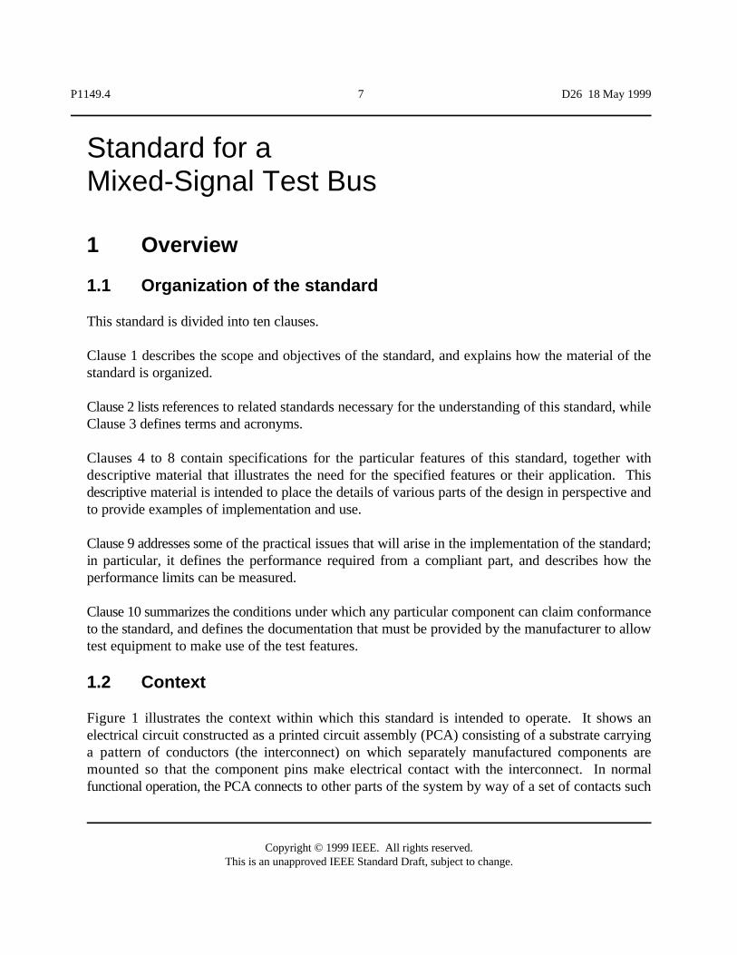
Figure 1 illustrates the context within which this standard is intended to operate. It shows anelectrical circuit constructed as a printed circuit assembly (PCA) consisting of a substrate carryinga pattern of conductors (the interconnect) on which separately manufactured components aremounted so that the component pins make electrical contact with the interconnect. In normalfunctional operation, the PCA connects to other parts of the system by way of a set of contacts such
P1149.4 8 D26 18 May 1999
Copyright © 1999 IEEE. All rights reserved.This is an unapproved IEEE Standard Draft, subject to change.
Figure 1: Mixed-signal printed circuit assembly
as the edge-connector shown in Figure 1.
In Figure 1, the component that is the subject of this standard is shown shaded. In a typical mixed-signal PCA, the pins of the component may be connected to
C other mixed-signal components (labelled M), which may or may not conform to thisstandard;
C digital components (labelled D), which may or may not conform to IEEE Std 1149.1;
C analog components (labelled A), which could be anything from a single transistor to anoperational amplifier or an analog signal processing circuit, but which would be unlikely tocontain any associated testability features;
C discrete components (labelled C), such as pull-up resistors or coupling capacitors, whichwill not have any associated testability features.
The PCA is tested, both in production (to verify correct manufacture) and in field service (to detectand locate faults), using automatic test equipment (ATE) to supply test signals to, and to collect testresponses from, some or all of the component pins. The aim of the test structures described in thisstandard is to provide test access to individual component pins from the edge-connector, so as toreduce or eliminate the need for the ATE to make direct physical contact via mechanical probes. Theextent to which this aim can be satisfied will depend on the make-up of the PCA : the pins of those
P1149.4 9 D26 18 May 1999
Copyright © 1999 IEEE. All rights reserved.This is an unapproved IEEE Standard Draft, subject to change.
components that conform either to this standard or to IEEE Std 1149.1 will be accessible from theedge-connector, and this will provide at least partial access to the pins of some non-conformantcomponents. If this is inadequate for testing purposes, additional probe access would need to beemployed.
1.3 Scope of the standard
1.3.1 Aims
This standard defines test features to be included in a mixed-signal (analog and digital) component,together with associated test protocols, to provide standardized approaches to :
P Interconnect Test : Testing for opens and shorts among the interconnections in a PCA;
P Parametric Test : Making analog characterization measurements, and testing for presenceand value of discrete components in a PCA;
P Internal Test : Testing the internal circuitry of the mixed-signal component itself whetheror not it is part of a PCA.
The standard does not mandate implementation details of the test circuitry, although examples ofconformant implementations are given for illustrative purposes.
1.3.2 Interconnect testing
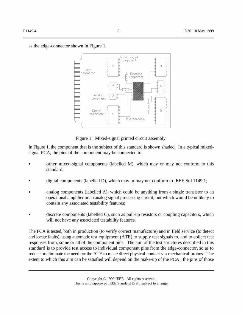
IEEE Std 1149.1 provides an effective mechanism for interconnect testing of a PCA populated withdigital components. The first objective of this new standard is to provide a similar capability for anassembly such as that illustrated in Figure 1, populated with analog, digital, and mixed-signalcomponents, together with discrete components. In seeking to satisfy this objective, one of the fundamental requirements is to provide the ability todetect open circuits in the interconnections between integrated circuits, and to detect and diagnosebridging faults anywhere in the interconnect regardless of whether they normally carry digital oranalog signals. The aim also is to provide a structure that allows testing in full compatibility withIEEE Std 1149.1, so as to permit mixed-signal interconnect testing to take place at the same time,and using the same procedures, as digital interconnect testing.
P1149.4 10 D26 18 May 1999
Copyright © 1999 IEEE. All rights reserved.This is an unapproved IEEE Standard Draft, subject to change.
Figure 2: Defects on a mixed-signal PCA
The range of problems is illustrated in Figure 2, which shows a group of interconnected componentsmounted on a board or other substrate, analog and digital pins being represented by “A” and “D”respectively. The left hand side of Figure 2 shows open circuits in analog and digital lines and alsoin an analog interconnection network. The right hand side of Figure 2 shows a number of shortcircuits : it should particularly be noticed that short circuits can occur between analog and analog,digital and digital, and analog and digital lines, as well as across discrete components ininterconnection networks.
1.3.3 Parametric Test
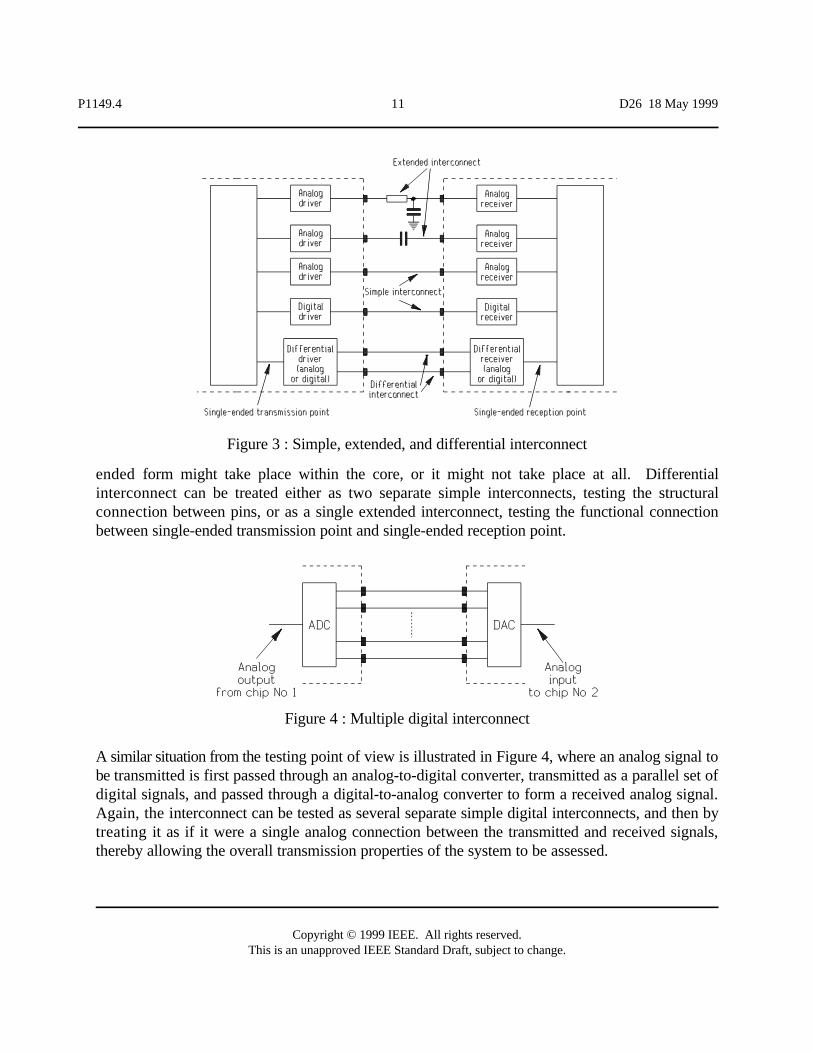
The second objective of this standard, parametric test, recognizes the fact that groups of one or morediscrete components are often interposed between integrated circuits, performing functions such aslevel shifting, passive filtering, and ac coupling. The inclusion of discrete components in theinterconnection pathway gives rise to the concept of “extended” (as opposed to “simple”)interconnect, as illustrated in Figure 3 : to provide for the testing of components in an extendedinterconnect, the standard defines a framework that will support analog measurements, allowing, forexample, impedances of discrete components to be computed. Meeting this objective also allowstesting of components such as pull-ups and filter capacitors associated with either analog or digitalcomponents.
Also illustrated in Figure 3 is an example of differential interconnect, which is a pair of pathwayscarrying signals whose information content is defined by the pair of signals rather than by either onesignal individually. In the case of digital differential interconnect, these pathways would normally beexcited by a single signal, and the activity would be converted back to a single signal after reception.Analog differential interconnect could follow the same pattern, but conversion from or to a single-
P1149.4 11 D26 18 May 1999
Copyright © 1999 IEEE. All rights reserved.This is an unapproved IEEE Standard Draft, subject to change.
Figure 3 : Simple, extended, and differential interconnect
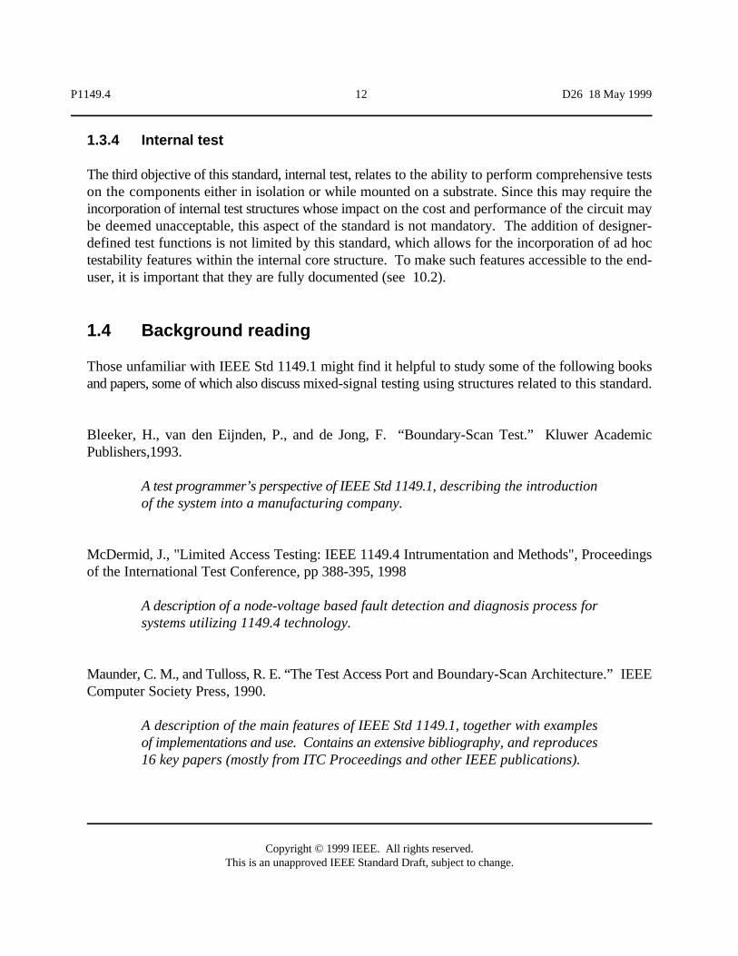
Figure 4 : Multiple digital interconnect
ended form might take place within the core, or it might not take place at all. Differentialinterconnect can be treated either as two separate simple interconnects, testing the structuralconnection between pins, or as a single extended interconnect, testing the functional connectionbetween single-ended transmission point and single-ended reception point.
A similar situation from the testing point of view is illustrated in Figure 4, where an analog signal tobe transmitted is first passed through an analog-to-digital converter, transmitted as a parallel set ofdigital signals, and passed through a digital-to-analog converter to form a received analog signal.Again, the interconnect can be tested as several separate simple digital interconnects, and then bytreating it as if it were a single analog connection between the transmitted and received signals,thereby allowing the overall transmission properties of the system to be assessed.
P1149.4 12 D26 18 May 1999
Copyright © 1999 IEEE. All rights reserved.This is an unapproved IEEE Standard Draft, subject to change.
1.3.4 Internal test
The third objective of this standard, internal test, relates to the ability to perform comprehensive testson the components either in isolation or while mounted on a substrate. Since this may require theincorporation of internal test structures whose impact on the cost and performance of the circuit maybe deemed unacceptable, this aspect of the standard is not mandatory. The addition of designer-defined test functions is not limited by this standard, which allows for the incorporation of ad hoctestability features within the internal core structure. To make such features accessible to the end-user, it is important that they are fully documented (see 10.2).
1.4 Background reading
Those unfamiliar with IEEE Std 1149.1 might find it helpful to study some of the following booksand papers, some of which also discuss mixed-signal testing using structures related to this standard.
Bleeker, H., van den Eijnden, P., and de Jong, F. “Boundary-Scan Test.” Kluwer AcademicPublishers,1993.
A test programmer’s perspective of IEEE Std 1149.1, describing the introductionof the system into a manufacturing company.
McDermid, J., "Limited Access Testing: IEEE 1149.4 Intrumentation and Methods", Proceedingsof the International Test Conference, pp 388-395, 1998
A description of a node-voltage based fault detection and diagnosis process forsystems utilizing 1149.4 technology.
Maunder, C. M., and Tulloss, R. E. “The Test Access Port and Boundary-Scan Architecture.” IEEEComputer Society Press, 1990.
A description of the main features of IEEE Std 1149.1, together with examplesof implementations and use. Contains an extensive bibliography, and reproduces16 key papers (mostly from ITC Proceedings and other IEEE publications).
P1149.4 13 D26 18 May 1999
Copyright © 1999 IEEE. All rights reserved.This is an unapproved IEEE Standard Draft, subject to change.
Parker, K. P., "The Boundary-Scan Handbook, 2nd Edition, Analog and Digital." Kluwer AcademicPublishers, 1998.
A description of the design and use of IEEE Std 1149.1 and of this standard,written from the point of view of practicing test engineers.
Parker, K.P., McDermid, J.E., and Oresjo, S. “Structure and Metrology for an Analog TestabilityBus.” Proceedings of the International Test Conference, pp 309 - 322, 1993.
A detailed description of a metrology whereby the values of componentsconnected between integrated circuits may be calculated, using a test structuresimilar to the one described in this standard.
P1149.4 14 D26 18 May 1999
Copyright © 1999 IEEE. All rights reserved.This is an unapproved IEEE Standard Draft, subject to change.
2 References
This standard shall be used in conjunction with the following publications.
IEEE Std 1149.1-1990 (includes IEEE Std 1149.1a-1993), IEEE Standard Test Access Port andBoundary-Scan Architecture.
IEEE Std 1149.1b-1994 Supplement to IEEE Std 1149.1-1990 IEEE Standard Test Access Po rtand Boundary-Scan Architecture.
NOTE - All IEEE standards are revised periodically. The next revision of IEEE Std 1149.1 will contain updated versions ofall the material at present contained in IEEE Std 1149.1a and IEEE Std 1149.1b, and is expected to be fully consistent withthe present standard.
IEEE Std 100-1996, IEEE Standard Dictionary of Electrical and Electronics Terms.
P1149.4 15 D26 18 May 1999
Copyright © 1999 IEEE. All rights reserved.This is an unapproved IEEE Standard Draft, subject to change.
3 Definitions, acronyms, and voltage symbols
3.1 Definitions
The following terms are used within this standard.
3.1.1 analog boundary module (ABM) : a circuit module connected between the core circuitand an analog function pin to provide facilities for test in a mixed-signal integrated circuit.See : core circuit, function pin, mixed-signal circuit.
NOTE -An ABM may be attached to a digital function pin in order to provide analog measurement capability tothe pin.
3.1.2 analog pin : a pin on an integrated circuit or other component that is intended to passinformation represented as a current or voltage that can have any value between the limitsdefined by the driver or receiver to which it is connected. Contrast with : digital pin.
NOTE 1 - Analog pins can have several forms. In addition to input, output, and bidirectional pins which areanalogous to corresponding digital forms, it is possible to have pins that do not readily fit into any of thesecategories (e.g., those supporting compensation elements for operational amplifiers). Any such pin that has noidentifiable drive capability should be regarded for the purposes of this standard as an input pin.
NOTE 2 - An analog pin may be put into a state in which no signals can pass in either direction between the pinand the core circuit. See : high-Z, core circuit, core disconnect.
NOTE 3 - An analog pin can pass digital data, using discrete levels that lie within its analog range.
3.1.3 analog test access port (ATAP) : a set of two mandatory and two optional pins on amixed-signal integrated circuit. The pins are connected to a bus allowing automatic testequipment to gain access to on-chip analog test facilities. The mandatory pins are labelledAT1 and AT2; the optional pins (labelled AT1N and AT2N) are normally used fordifferential testing.
3.1.4 CD State : the state of an analog pin when it is isolated from the core circuit and all testcircuits. See also : core disconnect, residual element.
NOTE - When a pin is in the CD state, there may be residual elements to which it remains connected.
3.1.5 compliance-enable pins : a set of one or more pins on a component such that fullcompliance with the rules of this standard is assured only when a defined pattern of enable
P1149.4 16 D26 18 May 1999
Copyright © 1999 IEEE. All rights reserved.This is an unapproved IEEE Standard Draft, subject to change.
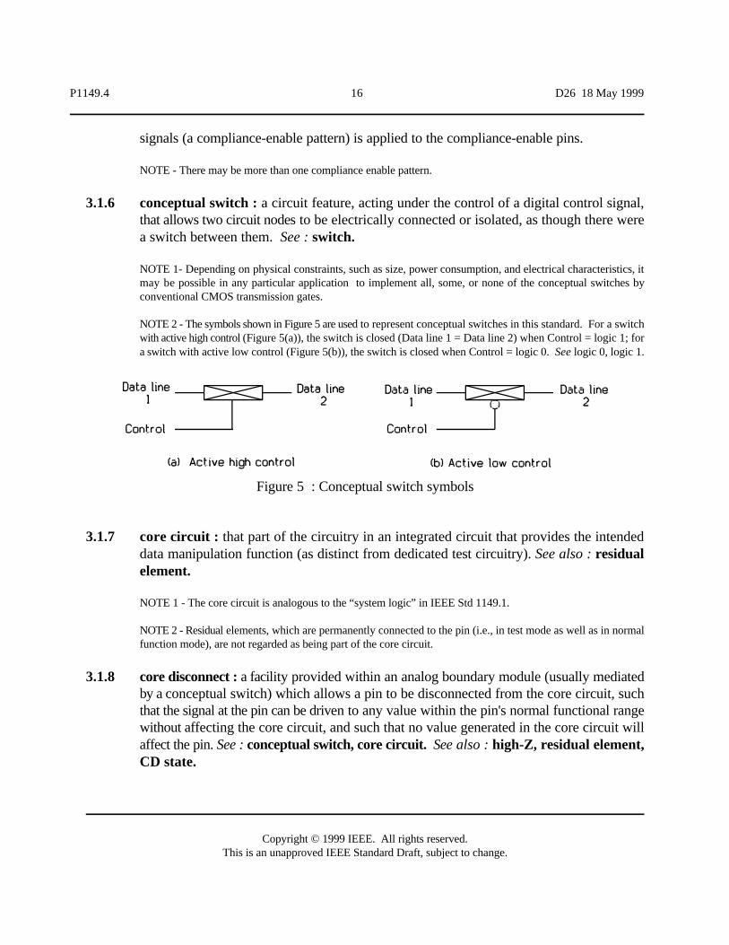
Figure 5 : Conceptual switch symbols
signals (a compliance-enable pattern) is applied to the compliance-enable pins.
NOTE - There may be more than one compliance enable pattern.
3.1.6 conceptual switch : a circuit feature, acting under the control of a digital control signal,that allows two circuit nodes to be electrically connected or isolated, as though there werea switch between them. See : switch.
NOTE 1- Depending on physical constraints, such as size, power consumption, and electrical characteristics, itmay be possible in any particular application to implement all, some, or none of the conceptual switches byconventional CMOS transmission gates.
NOTE 2 - The symbols shown in Figure 5 are used to represent conceptual switches in this standard. For a switchwith active high control (Figure 5(a)), the switch is closed (Data line 1 = Data line 2) when Control = logic 1; fora switch with active low control (Figure 5(b)), the switch is closed when Control = logic 0. See logic 0, logic 1.
3.1.7 core circuit : that part of the circuitry in an integrated circuit that provides the intendeddata manipulation function (as distinct from dedicated test circuitry). See also : residualelement.
NOTE 1 - The core circuit is analogous to the “system logic” in IEEE Std 1149.1.
NOTE 2 - Residual elements, which are permanently connected to the pin (i.e., in test mode as well as in normalfunction mode), are not regarded as being part of the core circuit.
3.1.8 core disconnect : a facility provided within an analog boundary module (usually mediatedby a conceptual switch) which allows a pin to be disconnected from the core circuit, suchthat the signal at the pin can be driven to any value within the pin's normal functional rangewithout affecting the core circuit, and such that no value generated in the core circuit willaffect the pin. See : conceptual switch, core circuit. See also : high-Z, residual element,CD state.
P1149.4 17 D26 18 May 1999
Copyright © 1999 IEEE. All rights reserved.This is an unapproved IEEE Standard Draft, subject to change.
NOTE 1 - The core disconnect facility could be provided as part of the functional driver or receiver attached to thepin, e.g., by implementing a driver with high-Z capability.
NOTE 2 - It is necessary to document all residual elements that remain connected to the pin when it enters the CDstate.
3.1.9 differential interconnect : a pair of connections carrying signals from a transmitter on onecomponent to a receiver on another component, where the transmitted information (whichmay be either analog or digital) is represented by the difference between two signals ratherthan by either signal individually. See also : simple interconnect; extended interconnect.
3.1.10 digital boundary module (DBM) : a circuit module connected between the digital corecircuit and a digital function pin to provide facilities for test in a digital or mixed-signalcomponent. A DBM serves the same function as, and conforms to the same rules as, theboundary-scan register cells defined in IEEE Std 1149.1.
NOTE 1 - A DBM may contain one or more boundary-scan register cells as explained in IEEE Std 1149.1.
NOTE 2 - A DBM may also be interposed at the boundary between the digital and analog portions of the corecircuit.
NOTE 3 - A control-and-observe DBM includes a switching function in the serial data path between pin and core;an observe-only DBM captures data from the data path without interrupting it.
3.1.11 digital pin : a pin on an integrated circuit or other component that is intended to pass datarepresented as a voltage or current that can have one of two discrete values. Contrastwith : analog pin.
NOTE 1 - In this standard the two discrete values are referred to as logic 0 and logic 1. See : logic 0, logic 1.
NOTE 2 - In addition to the set of discrete data values, a digital pin may be put into a state in which its driver isdisabled, so that it cannot actively sink or source current, and therefore cannot influence the state of the attachednet. See : high-Z, net.
NOTE 3 - If analog data is applied externally to a digital input pin, the internal circuitry will normally interpretthe data as digital. Use of the pin in this way will need to have due regard to possible adverse effects on theinternal circuitry (e.g., power consumption).
NOTE 4 - A digital function pin may have additional circuitry to allow analog signals to be applied or monitoredfor test purposes. This would not affect its status as a digital pin.
3.1.12 discrete component : an electrical element that is mounted on a printed circuit board orother substrate and connected to the interconnect wiring system, but which is not integratedto any significant extent with other elements, and does not contain boundary module test

P1149.4 18 D26 18 May 1999
Copyright © 1999 IEEE. All rights reserved.This is an unapproved IEEE Standard Draft, subject to change.
circuitry adjacent to its pins. See : interconnect.
3.1.13 extended interconnect : a connection pathway consisting of two or more nets that includesone or more discrete components. See : net. Contrast with : simple interconnect. Seealso : discrete component.
NOTE - The test requirement is to verify both the integrity of the connections and the values of the components.
3.1.14 function pin : an analog or digital pin on an integrated component that takes data intoand/or out of the core circuit when operating in normal function mode. Syn : mission pin,system pin.
NOTE : All pins carrying signals that affect the behaviour of the component, including reference supply pins butexcluding power supply pins and compliance-enable pins, are regarded as function pins.
3.1.15 high-Z : a condition in which the driver on a pin is inactive. The state of a net attached toa pin that is at high-Z is determined by values applied to other parts of the net. See : net.Contrast with : CD state. See also : core disconnect.
NOTE : For the purpose of this standard, the impedance looking in to a pin that is at high-Z must be > 1MS forany signal between V and V at any frequency up to 10 kHz.DD SS
3.1.16 in-circuit testing : A method of testing a printed circuit assembly by making direct physicalcontact between automatic test equipment and nets that are connected to the pins ofindividual components. See : net.
3.1.17 interconnect : the system of wiring that carries data and control signals between thedifferent components mounted on a printed circuit assembly. See also : simpleinterconnect; extended interconnect; differential interconnect.
3.1.18 internal test bus : the system of wiring that carries analog test signals around the interiorof an integrated circuit. See : test bus interface circuit.
3.1.19 logic 0, logic 1 : The two logic voltage levels for digital signals. In positive logic systems,the more positive of the two logic voltage levels is taken to be logic 1.
NOTE 1 - For convenience, positive logic is assumed throughout this standard.
NOTE 2 - The voltage levels representing logic 0 and logic 1 are not necessarily the same at every function pin.
NOTE 3 - logic 0 and 1 are often represented as LO and HI respectively.

P1149.4 19 D26 18 May 1999
Copyright © 1999 IEEE. All rights reserved.This is an unapproved IEEE Standard Draft, subject to change.
3.1.20 mixed-signal circuit : a circuit in which some variables are represented by analog(continuously variable) quantities, and some variables are represented by digital (discrete)quantities.
3.1.21 net : an interconnection path between component pins, where the resistance of the path isnot significantly different from zero.
3.1.22 reference quality voltage : dc source capable of sourcing and sinking current over adefined range without appreciable change of voltage, and whose stability over a given timeinterval is guaranteed.
NOTE - Whether or not a given voltage source is of reference quality has a major impact on the accuracy of themeasurement capabilities of the structures described in this standard.
3.1.23 residual element : a circuit element that is part of a network connected to one or morefunction pins, and that, for operational reasons, cannot be isolated from the pins in testmode. The network of residual elements can be connected to power supply pins as well asto function pins, provided it can be modelled, over a defined working range, by a networkof ideal resistors, capacitors, and inductors together with independent dc sources.
3.1.24 simple interconnect : a connection between two or more component pins consisting onlyof a net. Contrast with : extended interconnect.
3.1.25 switch : in the context of this standard, a switch is an electronic device connected betweentwo data lines. It can exist in one of two states, referred to as "open" and "closed", thestate at any time depending on a digital control variable. When the switch is open, thepathway between the two data lines has a very high impedance (ideally infinite), so thatsignals appearing on the data lines should be completely independent. When the switch isclosed, the pathway between the two data lines has a very low impedance (ideally zero), sothat signals on the two data lines should be identical.
NOTE 1 - Practical electronic switches implemented in silicon depart from the ideal in at least three ways.
(a) In the “on” state, the pathway between the two data lines may have significant impedance, or therelationship between voltage and current may be non-linear (e.g., a voltage-dependant “impedance”).
(b) In the “off” state, there may be significant interaction between the signals on the two data lines dueto (e.g.) stray capacitance.
(c) In either state there may be significant leakage pathways through which current can pass from the data
P1149.4 20 D26 18 May 1999
Copyright © 1999 IEEE. All rights reserved.This is an unapproved IEEE Standard Draft, subject to change.
lines to the surrounding circuitry or vice-versa.
The effects of all these characteristics will need to be considered as part of the detailed implementation, especiallyin a system containing multiple-switch networks.
NOTE 2 - A switching action effectively in series with the function signal pathway can sometimes be obtainedwithout a physically separate device by incorporating a high-Z or enable facility into the functional circuitry. See :conceptual switch, high-Z.
NOTE 3 - Data transmission through a switch is normally assumed to be bi-directional (as with electromechanicaldevices such as relays or semiconductor switches such as transmission gates). Some forms of switch canimplement only uni-directional voltage or current dependence.
3.1.26 test access port (TAP) : The test access port defined by IEEE Std 1149.1. Contrast with :ATAP.
3.1.27 test bus interface circuit (TBIC) : a circuit module that allows an internal analog test busin an integrated circuit to be isolated from or connected to the pins in the ATAP.See : ATAP.
3.1.28 test data : data that is entered into an electronic system of any kind (component, printedcircuit assembly, sub-system, system) for the purpose of verifying the integrity of part orall of the system. Test data may be entered through function pins or test pins or both.
3.1.29 test pin : a pin on a component or a printed circuit assembly that is provided solely orprimarily for use during test or maintenance operations.
3.2 Acronyms
ABM : Analog Boundary Module
ATAP : Analog Test Access Port
ATE : Automatic Test Equipment
CUT : Circuit Under Test
DBM : Digital Boundary Module
PCA : Printed Circuit Assembly
P1149.4 21 D26 18 May 1999
Copyright © 1999 IEEE. All rights reserved.This is an unapproved IEEE Standard Draft, subject to change.
TBIC : Test Bus Interface Circuit
TAP : Test Access Port
3.3 Voltage source symbols
Several voltage sources are required as part of the internal test structure described in this standard.The symbols used to denote these voltage sources are defined below. All of these sources are, ingeneral, pin-specific,
V : a fixed voltage that can be applied to internal test buses when not in use to reduce theclamppossibility of noise, crosstalk, or feedback.
V : a pin-specific reference quality voltage that is supplied to a component at a pin. AnyGfunction pin can be connected to V through its analog boundary module. See : referenceGquality voltage.
NOTE - V would normally be one of the power supply rail voltages.G
V ,V : two dc voltages used as test signals on analog pins during interconnect testing andH Lcomponent measurement.
NOTE 1 - V and V are pin-specific, and typically V > V . H L H L
NOTE 2 - At output pins, V and V will be supplied from the functional driver, and will correspond to logic 1 andH Llogic 0 respectively.
V : A pin-specific voltage to which the voltage at a function pin is compared. The result of theTHcomparison is a binary value that can be captured in the boundary-scan register.
The meaning of other terms used in this standard shall be as defined in IEEE Std 100-1996.
P1149.4 22 D26 18 May 1999
Copyright © 1999 IEEE. All rights reserved.This is an unapproved IEEE Standard Draft, subject to change.
4 Testability Architecture
4.1 Overview
4.1.1 Specification
Rules
(a) The component shall conform to all provisions of IEEE Std 1149.1 except wherespecifically noted herein.
NOTE 1 - This rule implies that a component conforming to this standard must contain a TAP to provide accessto the circuit for digital test signals. This TAP will contain three input lines (TDI, TCK, TMS), and one outputline (TDO); it may contain an optional fourth input line (TRST*).
NOTE 2 - In accordance with the rules of IEEE Std 1149.1, a component may require the application of aparticular pattern of signals (a compliance-enable pattern) to a set of one or more compliance-enable pins beforethe component is brought into full compliance with this standard. There may be more than one compliance-enablepattern for a particular component.
NOTE 3 - The version of IEEE Std 1149.1 referenced in Clause 2 makes little provision for testing the analogportions of a mixed-signal chip, and contains a few rules relating to analog pins that are not compatible with theprovisions of this standard. These inconsistencies are indicated in this standard, and may be resolved in a futurerevision of IEEE Std 1149.1.
(b) The interpretation of the rules governing those structures and facilities that are common tothis standard and to IEEE Std 1149.1 shall be determined by IEEE Std 1149.1.
NOTE - This rule implies that, when implementing this standard, the structure and performance of those elementsdescribed in IEEE Std 1149.1 must be in accordance with the specifications set out in IEEE Std 1149.1.
4.1.2 Description
This standard is an extension of IEEE Std 1149.1, and consists of additional structures to be addedto an IEEE Std 1149.1-conformant chip. Components that are conformant with this standard, whenmounted on a common substrate together with IEEE Std 1149.1-conformant chips, allow commontest operations (in particular, simple interconnect testing) to be performed in a consistent and co-ordinated manner.
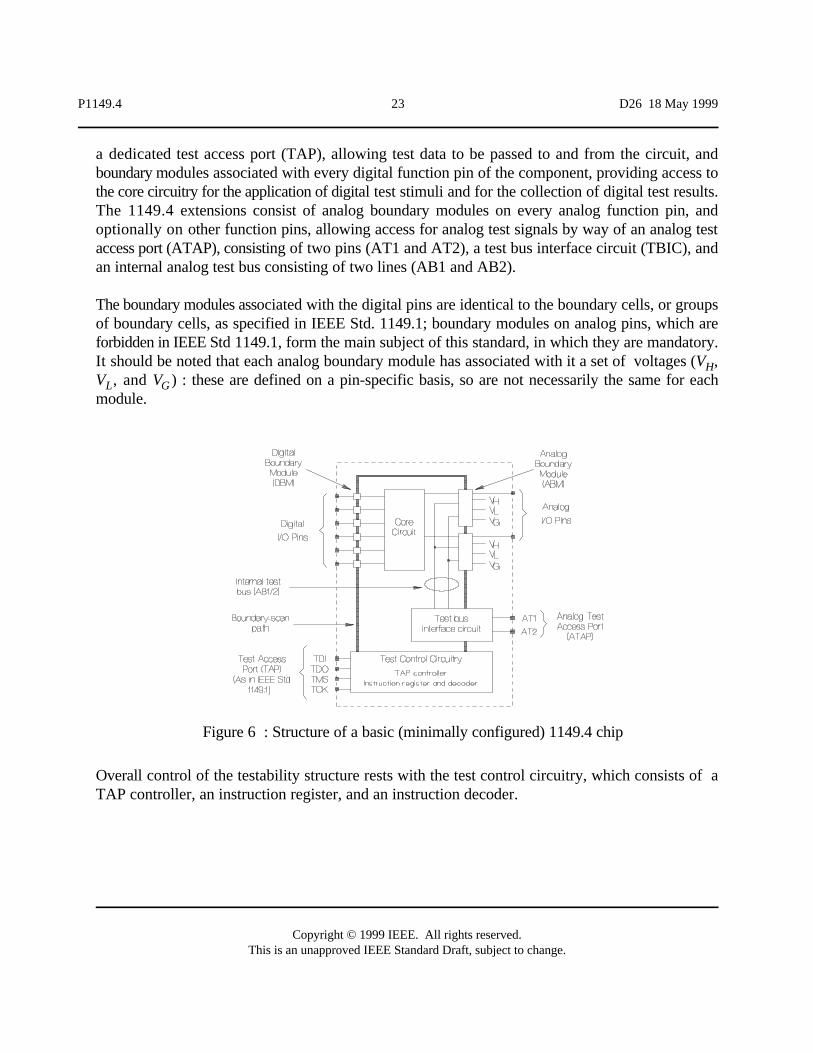
The overall structure of a basic 1149.4-conformant component is illustrated in Figure 6, which showsthe main mandatory elements of the standard. In IEEE Std 1149.1, the main testability features are
P1149.4 23 D26 18 May 1999
Copyright © 1999 IEEE. All rights reserved.This is an unapproved IEEE Standard Draft, subject to change.
Figure 6 : Structure of a basic (minimally configured) 1149.4 chip
a dedicated test access port (TAP), allowing test data to be passed to and from the circuit, andboundary modules associated with every digital function pin of the component, providing access tothe core circuitry for the application of digital test stimuli and for the collection of digital test results.The 1149.4 extensions consist of analog boundary modules on every analog function pin, andoptionally on other function pins, allowing access for analog test signals by way of an analog testaccess port (ATAP), consisting of two pins (AT1 and AT2), a test bus interface circuit (TBIC), andan internal analog test bus consisting of two lines (AB1 and AB2).
The boundary modules associated with the digital pins are identical to the boundary cells, or groupsof boundary cells, as specified in IEEE Std. 1149.1; boundary modules on analog pins, which areforbidden in IEEE Std 1149.1, form the main subject of this standard, in which they are mandatory.It should be noted that each analog boundary module has associated with it a set of voltages (V ,HV , and V ) : these are defined on a pin-specific basis, so are not necessarily the same for eachL Gmodule.
Overall control of the testability structure rests with the test control circuitry, which consists of aTAP controller, an instruction register, and an instruction decoder.
P1149.4 24 D26 18 May 1999
Copyright © 1999 IEEE. All rights reserved.This is an unapproved IEEE Standard Draft, subject to change.
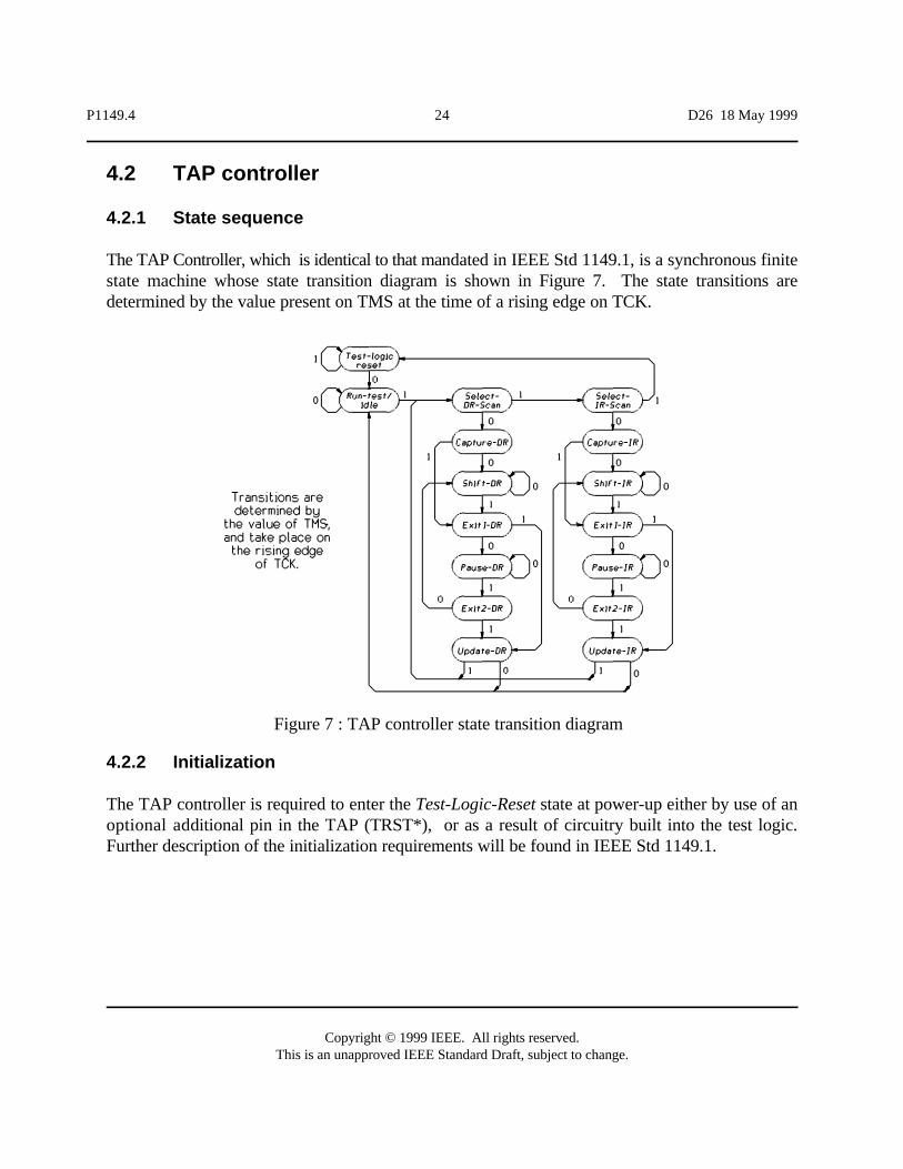
Figure 7 : TAP controller state transition diagram
4.2 TAP controller
4.2.1 State sequence
The TAP Controller, which is identical to that mandated in IEEE Std 1149.1, is a synchronous finitestate machine whose state transition diagram is shown in Figure 7. The state transitions aredetermined by the value present on TMS at the time of a rising edge on TCK.
4.2.2 Initialization
The TAP controller is required to enter the Test-Logic-Reset state at power-up either by use of anoptional additional pin in the TAP (TRST*), or as a result of circuitry built into the test logic.Further description of the initialization requirements will be found in IEEE Std 1149.1.
P1149.4 25 D26 18 May 1999
Copyright © 1999 IEEE. All rights reserved.This is an unapproved IEEE Standard Draft, subject to change.
4.2.3 Controller outputs
4.2.3.1 Specification
Rules
(a) The TAP controller shall generate signals to control the operation of the TBIC as definedin 6.3.
(b) The TAP controller shall generate signals to control the operation of the ABMs andassociated circuitry as defined in 7.3.5.
(c) When the TAP controller is in the Test-Logic-Reset state, all function pins shall be isolatedfrom the analog test buses, and from V , V , and V , irrespective of the state of the ABMH L Gcontrol register bits.
(d) When the TAP controller is in the Test-Logic-Reset state, all ATAP pins shall be isolatedfrom the analog test buses, and from V , V , and V , irrespective of the state of theH L clampTBIC control register bits.
4.2.3.2 Description
Control signals for routing data, reconfiguring the test circuitry, and exerting control over the TAP,the ATAP, and the TBIC, are derived partly from output logic of the TAP controller, and partly fromthe instruction register. In addition, the TBIC and each ABM contains an individual control register,so that its mode of operation can be individually controlled (see Clauses 6 and 7.3.) The instructionregister, the ABM control registers, and the TBIC control register are all loaded through the TAP.
The precise set of signals required to control the test structure and boundary modules associated withdigital function pins is not specified in IEEE Std 1149.1 except in terms of example implementations.Boundary modules are not required by the standard to support all instructions; the control signalsneeded will vary depending on the particular set of instructions supported by the individualcomponent. These signals occur on either the rising or the falling edge of TCK in each controllerstate as specified in IEEE Std 1149.1. All the example implementations of boundary-scan register cells described in IEEE Std 1149.1 usecontrol signals ShiftDR and ClockDR; all those that incorporate the update register also useUpdateDR. Other control signals needed for the correct operation of the analog test structure willneed to be generated by adding appropriate output logic to the TAP controller.
P1149.4 26 D26 18 May 1999
Copyright © 1999 IEEE. All rights reserved.This is an unapproved IEEE Standard Draft, subject to change.
NOTE - Some output signals named in the example implementations of IEEE Std 1149.1, and also referred to in this standard,have the same names as some controller states. Throughout this standard, where this applies, control signals are shown innormal case (e.g., ShiftDR), and controller states are shown in italics (e.g., Shift-DR).
4.3 Analog test access port (ATAP)
4.3.1 Specification
Rules
(a) Each component shall contain an ATAP.
(b) The ATAP shall include two analog test pins, AT1 and AT2 (defined in Clause 6).
(c) AT1 and AT2 shall be dedicated pins (i.e., they shall not be used for any other purpose).
Permission
(d) The ATAP may contain two further analog test pins, AT1N and AT2N, to allow for thetesting of differential input and/or output. In this case, AT1 and AT1N shall form onedifferential pair, and AT2 and AT2N shall form the other differential pair.
4.3.2 Description
The ATAP is an analog port that provides access for analog test signals. Dedicated connections arerequired to allow access to the full range of mandatory features of this standard. The ATAP iscomposed of a minimum of 1 analog input connection and 1 analog output connection. Optionaladditional analog lines can provide additional capability (e.g., differential stimulus and/ormeasurement : see 8.1.3). The definition and properties of the test bus interface circuit (TBIC) arespecified in Clause 6.
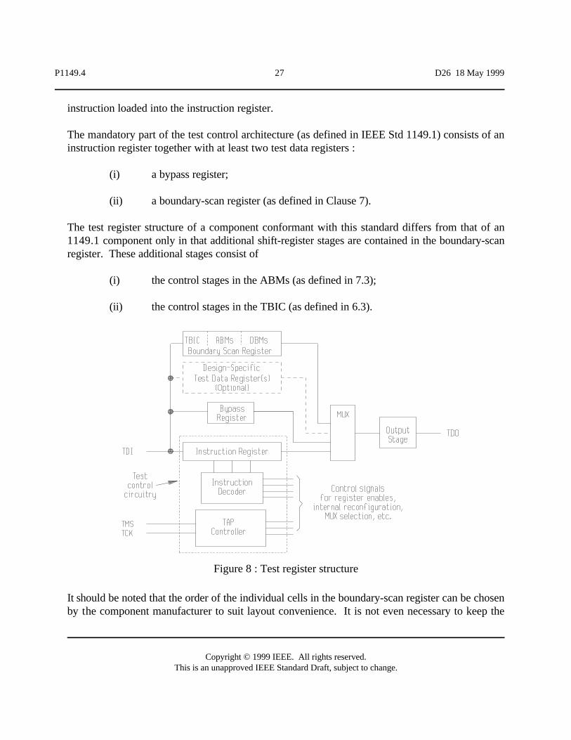
4.4 Register architecture
The test register architecture, shown in Figure 8, is essentially identical to that defined in IEEE Std1149.1. It is entirely digital, consisting essentially of a number of shift-register paths, connected inparallel with a common serial data input connected to TDI and a common serial data outputconnected to TDO. Control signals are required both for the transfer of data and for the choice ofwhich of the alternative parallel paths is active : these signals are supplied, as shown in Figure 8,partly by the TAP controller and partly by the instruction decoder, interpreting the particular
P1149.4 27 D26 18 May 1999
Copyright © 1999 IEEE. All rights reserved.This is an unapproved IEEE Standard Draft, subject to change.
Figure 8 : Test register structure
instruction loaded into the instruction register.
The mandatory part of the test control architecture (as defined in IEEE Std 1149.1) consists of aninstruction register together with at least two test data registers :
(i) a bypass register;
(ii) a boundary-scan register (as defined in Clause 7).
The test register structure of a component conformant with this standard differs from that of an1149.1 component only in that additional shift-register stages are contained in the boundary-scanregister. These additional stages consist of
(i) the control stages in the ABMs (as defined in 7.3);
(ii) the control stages in the TBIC (as defined in 6.3).
It should be noted that the order of the individual cells in the boundary-scan register can be chosenby the component manufacturer to suit layout convenience. It is not even necessary to keep the
P1149.4 28 D26 18 May 1999
Copyright © 1999 IEEE. All rights reserved.This is an unapproved IEEE Standard Draft, subject to change.
control stages belonging to a single ABM or to the TBIC together in a single block, since theindividual stages are identified by name.
An additional register (the device identification register) for part identification may be included, aswell as any number of design-specific test data registers to give access to design-specific testabilityfeatures. An example of a design-specific test register that could be included in a mixed-signal designwould be an internal scan register used to give access to internal nodes of the core.
Depending on the style of implementation of the test logic defined by this standard, circuitry may berequired to retime the signal passing through the output stage shown in Figure 8 to occur on thefalling edge of TCK.
P1149.4 29 D26 18 May 1999
Copyright © 1999 IEEE. All rights reserved.This is an unapproved IEEE Standard Draft, subject to change.
5 Instructions
5.1 General
5.1.1 Specification
Rule
(a) Each component shall provide a PROBE instruction. (See 5.3.4)
Permissions
(b) Additional instructions may be provided within the rules set out in this standard and inIEEE Std 1149.1.
(c) Any instruction code apart from all 1s and all 0s may be used to represent any instruction.
NOTE 1 - The instruction code consisting of all 1s is reserved for the BYPASS instruction.
NOTE 2 - The instruction code consisting of all 0s is reserved for the EXTEST instruction.
(d) Any instruction (including BYPASS and EXTEST) may be represented by more than oneinstruction code.
5.1.2 Description
An instruction is a bit-pattern that is loaded into the instruction register, and is then decoded by theinstruction decoder. It has two major functions : it defines the set of test data registers that mayoperate while the instruction is selected, and it defines the serial test data register path that is usedto shift data between TDI and TDO. The instruction set must include one instruction (PROBE)designed to support analog testing, together with the mandatory instructions from IEEE Std 1149.1(BYPASS, SAMPLE/PRELOAD, and EXTEST - some with extended facilities). It may also includeuser-defined instructions as well as optional instructions defined in IEEE Std 1149.1.
The remainder of this clause lists all defined instructions. Instructions that derive from IEEE Std1149.1 must satisfy the rules of IEEE Std 1149.1; the Rules, Recommendations, and Permissionslisted herein are additional to the specifications contained in IEEE Std 1149.1. The instruction thatis unique to this standard is fully specified and described; others are described in general terms forconvenience.
P1149.4 30 D26 18 May 1999
Copyright © 1999 IEEE. All rights reserved.This is an unapproved IEEE Standard Draft, subject to change.
5.2 Response of test logic to instructions
5.2.1 Specification
Rules
(a) Each component shall respond to the mandatory instructions of IEEE Std 1149.1 inaccordance with the rules contained in IEEE Std 1149.1, together with any additional ruleslisted herein.
(b) Each component shall respond to the PROBE instruction in accordance with the rules in thisstandard.
(c) If a component provides any optional instructions defined in IEEE Std 1149.1, its responseto those instructions shall be in accordance with the rules contained in IEEE Std 1149.1,together with any additional rules listed herein.
5.2.2 Description
The operation performed at any time by any particular DBM is determined in accordance with therules of IEEE Std 1149.1. The operation performed at any time by any particular ABM is determinednot only by the control signals supplied from the instruction decoder (which depend on the instructioncurrently loaded into the instruction register), but also by the control signals supplied by the TAPcontroller (which depend on the current state of the controller), and, depending on which instructionis selected, the values contained in the individual ABM control register.
The particular module design used in the test data registers (and the ABMs) will determine whatcontrol signals are required from the TAP controller and the instruction decoder. For the ABMdesign shown in Figure 23, for example, ShiftDR, ClockDR, and UpdateDR would be supplied bythe TAP controller; Mode1 and Mode2 would be supplied from the instruction decoder.
Each instruction is represented by one or more instruction codes, and defines a particular test dataregister to be selected for serial connection between TDI and TDO. All instructions are defined insuch a way that unselected test data registers have no effect on the operation of either the corecircuitry or the selected test data register, unless specifically mandated in the instruction definition.
When implementing the instruction decoder, it is important to consider possible effects of decodingspikes when changing from one instruction to another (e.g., from BYPASS to SAMPLE/PRELOAD),so that transitory instruction selections are avoided.
P1149.4 31 D26 18 May 1999
Copyright © 1999 IEEE. All rights reserved.This is an unapproved IEEE Standard Draft, subject to change.
5.3 Mandatory instructions
5.3.1 The BYPASS instruction
5.3.1.1 Specification
Rules
(a) When the BYPASS instruction is selected, all ATAP pins shall be isolated from the internalanalog test buses and from all test voltage sources, irrespective of the state of the boundaryregister bits.
(b) When the BYPASS instruction is selected, all analog function pins shall be connected to thecore circuit.
(c) When the BYPASS instruction is selected, all analog function pins shall be isolated from theinternal and external analog test buses and from all test voltage sources, irrespective of thestate of the boundary register bits.
5.3.1.2 Description
The BYPASS instruction selects the bypass register to be connected for serial access between TDIand TDO in the Shift-DR controller state. The BYPASS instruction can be selected by loading logic1 into every stage of the instruction register (this coding is mandatory; optionally, other codes mayalso be designed to select BYPASS).
When the BYPASS instruction is selected, test data registers that can operate in either system or testmode perform their system function, and the operation of the test logic has no effect on the actionof either the analog or the digital core circuitry.
P1149.4 32 D26 18 May 1999
Copyright © 1999 IEEE. All rights reserved.This is an unapproved IEEE Standard Draft, subject to change.
5.3.2 The SAMPLE/PRELOAD instruction
5.3.2.1 Specification
Rules
(a) When the SAMPLE/PRELOAD instruction is selected, all ATAP pins shall be isolated fromthe internal analog test buses and from all test voltage sources, irrespective of the state ofthe boundary register bits.
(b) When the SAMPLE/PRELOAD instruction is selected, all analog function pins shall beconnected to the core circuit.
(c) When the SAMPLE/PRELOAD instruction is selected, all analog function pins shall beisolated from the internal and external analog test buses and from all test voltage sources.
5.3.2.2 Description
This instruction has two functions. The first (SAMPLE) is to use the boundary-scan register to allowa snapshot to be taken of the data at the digital pins during normal operation. The snapshot is takenon the rising edge of TCK in the Capture-DR controller state, and can be examined serially by shiftingthrough TDO.
A digitized snapshot of the (analog) signal on an analog pin will be captured in SAMPLE/PRELOADby way of the one-bit digitizer in the ABM (see 7.3). The ability to monitor the analog signal itselfis provided by the PROBE instruction (see 5.3.4).
The second function of this instruction (PRELOAD) is to allow an initial digital data pattern to beloaded into the latched parallel outputs of the boundary-scan register prior to the selection of anotherboundary-scan test operation. The loading is performed on the falling edge of TCK in the Update-DRcontroller state. During the PRELOAD phase, the operation of the core circuit and the flow ofsignals between the function pins and the core circuit are unaffected by the test logic.
In the same way, a digital data pattern can be specified for each ABM, by loading the appropriatevalues into its control register, which is part of the boundary-scan register.
NOTE -A future revision of IEEE Std 1149.1may define SAMPLE and PRELOAD as separate instructions. In this case, theuser could effectively re-merge them by using the same instruction code for both.
P1149.4 33 D26 18 May 1999
Copyright © 1999 IEEE. All rights reserved.This is an unapproved IEEE Standard Draft, subject to change.
5.3.3 The EXTEST instruction
5.3.3.1 Specification
Rule
(a) When the EXTEST instruction is selected, each ABM shall be set so that the pin isdisconnected from the core (i.e., the core disconnect switch shall be open).
5.3.3.2 Description
The EXTEST instruction is used to test simple interconnect as in IEEE Std 1149.1 by applying logiclevels to all pins. It is also used to test extended interconnect by allowing automatic test equipment(ATE) to make measurements of discrete components connected to the pins. The facilitiesincorporated into the boundary-scan test structure allow the ATE to apply analog test signals andmonitor analog responses, and hence to obtain one of the major benefits of in-circuit testing withoutusing physical probing. This instruction is the central feature of this standard : the principlesunderlying its use for analog measurements are outlined in Clause 8.
The EXTEST instruction selects the boundary-scan register to be connected for serial access betweenTDI and TDO in the Shift-DR controller state. While the EXTEST instruction is selected, all functionoutput pins (analog and digital) are isolated from the core. This allows the signals driven from systemoutput pins to be completely defined by the data shifted into the corresponding boundary modules.Function input pins (analog and digital) are monitored by their boundary modules, and may beisolated from the core. If the facility to isolate input pins from the core during testing is notincorporated, the designer must ensure that signals appearing at an input pin during EXTESTexecution will not cause damage to the core, affect measurements on other pins, or be affected bycore signals.
The EXTEST instruction must be represented by the all 0s code, but may also be represented by othercode(s).
NOTE - Because it is mandatory for the all 0s code to represent EXTEST, a stuck-at-zero fault on TDI could then result in anunwanted selection of EXTEST. Future revisions of IEEE Std 1149.1 may remove the requirement for all 0s to representEXTEST.
P1149.4 34 D26 18 May 1999
Copyright © 1999 IEEE. All rights reserved.This is an unapproved IEEE Standard Draft, subject to change.
5.3.4 The PROBE instruction
5.3.4.1 Specification
Rules
(a) The PROBE instruction shall select the boundary-scan register to be connected for serialaccess between TDI and TDO in the Shift-DR controller state.
(b) When the PROBE instruction is selected, each DBM shall be set to allow core functions topropagate to and from the pins.
NOTE - This is similar to the requirements in SAMPLE/PRELOAD and BYPASS.
(c) When the PROBE instruction is selected, each ABM shall be set so that its pin is connectedto the core (i.e., the core disconnect switch shall be closed).
(d) When the PROBE instruction is selected, one or both of the ATAP pins shall be connectedto the corresponding internal analog test bus lines.
(e) When the PROBE instruction is selected, the internal analog test bus lines shall beconnected to individual function pins as determined by the contents of the correspondingABM control registers.
NOTE - The PRELOAD phase of the SAMPLE/PRELOAD instruction may be used to set up the contents of theABM and TBIC control registers before the PROBE instruction is activated.
5.3.4.2 Description
The PROBE instruction allows analog pins to be monitored on AB2, and/or stimulated from AB1,while the component is operating in its normal mission configuration, with all function pins connectedto the core.
P1149.4 35 D26 18 May 1999
Copyright © 1999 IEEE. All rights reserved.This is an unapproved IEEE Standard Draft, subject to change.
5.4 Optional instructions
5.4.1 The INTEST instruction
5.4.1.1 Specification
Rules
(a) While the INTEST instruction is selected, all inputs to the digital part of the core shall besupplied by data stored in the boundary-scan register, except clocks, which may be allowedto free-run provided that the component can be single-stepped through the test sequence.
NOTE - The PRELOAD phase of the SAMPLE/PRELOAD instruction may be used to set up the contents of theboundary-scan register (including the ABM control registers) before the INTEST instruction is selected.
(b) While the INTEST instruction is selected, all analog pins shall be connected to the analogcore.
NOTE - Because, in this mode of operation, much of the core is not isolated from the external circuitry, it may benecessary to control this external circuitry so as to avoid unwanted interference. Care should also be taken toensure that the core itself does not generate unwanted interference.
(c) While the INTEST instruction is selected, any analog pin shall be capable of being connectedto AB1.NOTE - Because there is normally only one analog test bus input line available, only one analog stimulus can besupplied, although, if desired, the signal at AB1 could be applied to more than one input pin.
(d) While the INTEST instruction is selected, those inputs to the analog core that are normallysupplied from the digital core shall receive data determined by the contents of thecorresponding DBMs.
NOTE - The PRELOAD phase of the SAMPLE/PRELOAD instruction may be used to set up the contents of theDBMs before the INTEST instruction is activated.
(e) While the INTEST instruction is selected, any analog pin shall be capable of beingmonitored by AB2.
NOTE - The signal monitored by AB2 may be affected by more than one input. It may be necessary to applyexternal control to those inputs that are not being driven by AB1.
P1149.4 36 D26 18 May 1999
Copyright © 1999 IEEE. All rights reserved.This is an unapproved IEEE Standard Draft, subject to change.
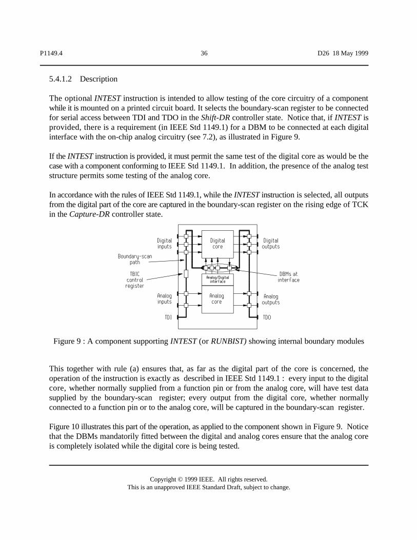
Figure 9 : A component supporting INTEST (or RUNBIST) showing internal boundary modules
5.4.1.2 Description
The optional INTEST instruction is intended to allow testing of the core circuitry of a componentwhile it is mounted on a printed circuit board. It selects the boundary-scan register to be connectedfor serial access between TDI and TDO in the Shift-DR controller state. Notice that, if INTEST isprovided, there is a requirement (in IEEE Std 1149.1) for a DBM to be connected at each digitalinterface with the on-chip analog circuitry (see 7.2), as illustrated in Figure 9.
If the INTEST instruction is provided, it must permit the same test of the digital core as would be thecase with a component conforming to IEEE Std 1149.1. In addition, the presence of the analog teststructure permits some testing of the analog core.
In accordance with the rules of IEEE Std 1149.1, while the INTEST instruction is selected, all outputsfrom the digital part of the core are captured in the boundary-scan register on the rising edge of TCKin the Capture-DR controller state.
This together with rule (a) ensures that, as far as the digital part of the core is concerned, theoperation of the instruction is exactly as described in IEEE Std 1149.1 : every input to the digitalcore, whether normally supplied from a function pin or from the analog core, will have test datasupplied by the boundary-scan register; every output from the digital core, whether normallyconnected to a function pin or to the analog core, will be captured in the boundary-scan register.
Figure 10 illustrates this part of the operation, as applied to the component shown in Figure 9. Noticethat the DBMs mandatorily fitted between the digital and analog cores ensure that the analog coreis completely isolated while the digital core is being tested.
P1149.4 37 D26 18 May 1999
Copyright © 1999 IEEE. All rights reserved.This is an unapproved IEEE Standard Draft, subject to change.
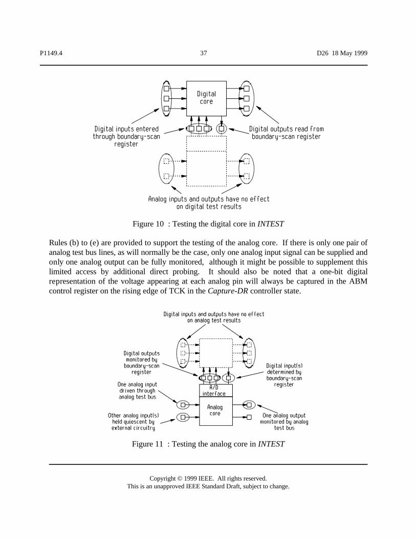
Figure 10 : Testing the digital core in INTEST
Figure 11 : Testing the analog core in INTEST
Rules (b) to (e) are provided to support the testing of the analog core. If there is only one pair ofanalog test bus lines, as will normally be the case, only one analog input signal can be supplied andonly one analog output can be fully monitored, although it might be possible to supplement thislimited access by additional direct probing. It should also be noted that a one-bit digitalrepresentation of the voltage appearing at each analog pin will always be captured in the ABMcontrol register on the rising edge of TCK in the Capture-DR controller state.
P1149.4 38 D26 18 May 1999
Copyright © 1999 IEEE. All rights reserved.This is an unapproved IEEE Standard Draft, subject to change.
A typical analog core test, as it might be applied to the circuit of Figure 9, is illustrated in Figure11. In this test, one of the analog outputs is being monitored through AT2 while one of the inputsis being supplied with an analog stimulus through AT1. Other inputs to the analog core include thesignals normally supplied by the digital core and those coming from other analog function pins. During INTEST, the digital signals will be supplied from the boundary-scan register (which will needto have appropriate data scanned in). Note 2 following rule (c) draws attention to the fact that allthe analog pins (including the one being stimulated by way of AB1) are connected to the externalcircuitry on the board. This circuitry may have to be controlled to provide appropriate operatingconditions, or to ensure that the input is rendered quiescent.
In addition to the analog output chosen for observation at AT2, digital test result data is captured inthe DBMs in the analog/digital interface, and digitized results are captured in the control registers ofall ABMs. This data is captured on the rising edge of TCK in the Capture-DR controller state.Further test results for the same stimulus conditions could be obtained by repeating the test whilemonitoring each analog output in turn.
5.4.2 Device identification register instructions
These instructions make use of the optional identification register to allow internally stored codes tobe read serially from TDO to identify the manufacturer, part number, and the version of the part. Asfar as the digital part is concerned, the behavior in response to these instructions of a componentclaiming conformance to this standard is identical to that of an IEEE Std 1149.1 component.Additional rules relating to the ATAP and the analog function pins are defined below.
5.4.2.1 The IDCODE instruction
5.4.2.1.1 Specification
Rules
(a) When the IDCODE instruction is selected, all ATAP pins shall be isolated from the analogtest buses, irrespective of the state of the boundary register bits.
(b) When the IDCODE instruction is selected, all analog function pins shall be connected to thecore.
(c) When the IDCODE instruction is selected, all analog function pins shall be isolated from
the internal and external analog test buses and from all test voltage sources.
P1149.4 39 D26 18 May 1999
Copyright © 1999 IEEE. All rights reserved.This is an unapproved IEEE Standard Draft, subject to change.
5.4.2.1.2 Description
If the device identification register is included in the design, then the IDCODE instruction must besupported. This instruction will then be loaded into the instruction register on the falling edge ofTCK following entry into the Test-Logic-Reset controller state. The instruction can also be loadedserially through TDI while in the Shift-IR controller state.
When the IDCODE instruction is selected, the manufacturer’s identification code is loaded into theidentification register on the rising edge of TCK following entry into the Capture-DR controller state,and can then be read serially through TDO.
5.4.2.2 The USERCODE instruction
5.4.2.2.1 Specification
Rules
(a) When the USERCODE instruction is selected, all ATAP pins shall be isolated from theanalog test buses, irrespective of the state of the boundary register bits.
(b) When the USERCODE instruction is selected, all analog function pins shall be connectedto the core.
(c) When the USERCODE instruction is selected, all analog function pins shall be isolated from
the internal and external analog test buses and from all test voltage sources.
5.4.2.2.2 Description
If the device identification register is included in the design, and if the component is user-programmable such that the programming cannot otherwise be determined by the test logic, then theUSERCODE instruction must be provided, and a user-programmed identification code must beincluded in the component. This code will, when the USERCODE instruction is selected, be loadedinto the identification register on the rising edge of TCK following entry into the Capture-DRcontroller state, and can then be read serially through TDO.
P1149.4 40 D26 18 May 1999
Copyright © 1999 IEEE. All rights reserved.This is an unapproved IEEE Standard Draft, subject to change.
5.4.3 The RUNBIST instruction
5.4.3.1 Specification
Rules
(a) The RUNBIST instruction shall be self-contained, and shall leave a single test resultsignature in the test data register selected by the RUNBIST instruction.
NOTE 1 - By self-contained is meant that no external stimulus is required apart from power and TAP signals.
NOTE 2 - The signature could be derived from a self-test conducted on the digital part of the core, whilemaintaining the analog part in a quiescent state; or the circuit could be designed to incorporate structures necessaryto support analog stimulus generation and result collection (and digitization) so as to produce a compositesignature.
NOTE 3 - The test data register will be selected by the designer. It could be the boundary-scan register.
(b) While RUNBIST is selected, analog function outputs shall behave in one of two ways.
(i) All output signals shall be defined by the data held in the boundary-scan register;
or (ii) Every output signal shall be placed in the inactive CD state, which may be High-Z.
NOTE - These options are the same as those offered in IEEE Std 1149.1 for digital output pins.
(c) The choice of output behavior ((b) above) shall be the same for analog and digital pins.
Recommendation
(d) The test result should be a multi-bit signature.
NOTE - The purpose of a multi-bit signature is to allow a failed self-test to record diagnostic information ratherthan a simple GO/NOGO decision.
5.4.3.2 Description
The RUNBIST instruction is optional but in IEEE Std 1149.1 it is recommended that either INTESTor RUNBIST should be supported. If RUNBIST is supported, it is required to be self-contained,executing while in the Run-Test/Idle controller state. It is required to leave, in the test data registerconnected between TDI and TDO (which could be the boundary-scan register), a test result signature
P1149.4 41 D26 18 May 1999
Copyright © 1999 IEEE. All rights reserved.This is an unapproved IEEE Standard Draft, subject to change.
that is independent of any external signals that may be present at any of the pins. A mixed-signalcircuit claiming conformance with this standard is required to provide exactly the same facilities.
5.4.4 The CLAMP instruction
5.4.4.1 Specification
Rules
(a) When the CLAMP instruction is selected, the state of all signals driven from analog functionoutput pins shall be defined by the data held in the corresponding ABMs.
(b) While the CLAMP instruction is selected, the data held in the ABMs shall not change.
(c) When the CLAMP instruction is selected, the state of the AT1/2 pins shall be defined by thedata held in the TBIC control register. (See 6.4).
5.4.4.2 Description
The optional CLAMP instruction selects the bypass register for connection between TDI and TDOin the Shift-DR controller state. While the CLAMP instruction is selected, the states of all signalsdriven from system output pins (analog and digital) are determined by the contents of the boundarymodules. (This data can be previously inserted, e.g. by using the PRELOAD phase of theSAMPLE/PRELOAD instruction.)
5.4.5 The HIGHZ instruction
5.4.5.1 Specification
Rules
(a) When the HIGHZ instruction is selected, all analog function pins shall be disconnected fromthe core and from all test circuitry (i.e., all switches in the ABM, including the coredisconnect switch, shall be open).
(b) When the HIGHZ instruction is selected, the AT1/2 pins shall be in the high impedancestate, regardless of the data held in the TBIC control register. (See 6.2).
P1149.4 42 D26 18 May 1999
Copyright © 1999 IEEE. All rights reserved.This is an unapproved IEEE Standard Draft, subject to change.
5.4.5.2 Description
The optional HIGHZ instruction selects the bypass register for connection between TDI and TDOin the Shift-DR controller state. While the HIGHZ instruction is selected, the component is put intoa state in which all the function outputs are placed in an inactive drive (CD or high impedance) state.The ATAP pins are also isolated from the internal test bus lines (see NOTE 2 of Table 2).
P1149.4 43 D26 18 May 1999
Copyright © 1999 IEEE. All rights reserved.This is an unapproved IEEE Standard Draft, subject to change.
6 The Test Bus Interface Circuit (TBIC)
6.1 General
The provision of facilities for the application and monitoring of analog test signals constitutes themain architectural feature of this standard. This clause describes the system of internal test buses tocarry signals within the circuit, and the analog test bus interface circuit (TBIC), which controls theconnections between the ATAP and the internal test buses. These elements provide a link betweenthe system of external test buses that carry signals to and from the automatic test equipment (ATE)by way of pins in the ATAP (see 4.3), and the analog boundary modules (ABMs) within thecomponent (see 7.3).
The simplest analog test structure that provides conformance with this standard consists of two pinsin the ATAP (AT1 and AT2) and two internal bus lines (AB1 and AB2). The specification of thisbus structure and its supporting TBIC is set out in 6.2 and 6.3. An optional extension that can beused for the testing of differential I/O is set out in 6.4 (although it should be noted that differentialI/O can be tested using modified boundary modules instead of using this optional extension - see 7.4);the use of partitioned internal buses is described in 6.5.
6.2 Test bus and TBIC structure
6.2.1 Specification
Rules
(a) There shall be two internal analog test bus lines (AB1 and AB2).
(b) The connection of the internal test bus lines to the ATAP pins shall be controlled by aTBIC.
(c) During normal (non-test) operation of the component, the internal analog test bus lines(AB1 and AB2) shall be isolated from the ATAP.
(d) While the internal analog test bus lines are isolated from the ATAP, they shall have no effecton the operation of the component.
(e) There shall be a switchable connection between AT1 and AB1 such that current derivedfrom an external source (e.g., an ATE) can be transmitted to AB1.
VH % VL
2±
VH & VL
4
P1149.4 44 D26 18 May 1999
Copyright © 1999 IEEE. All rights reserved.This is an unapproved IEEE Standard Draft, subject to change.
(f) There shall be a switchable connection between AB2 and AT2 such that a voltagedeveloped on AB2 can be monitored by an external measurement system (e.g., an ATE)connected to AT2.
(g) There shall be a switchable connection between AT1 and AT2 via AB1 such that currentderived from an external source (e.g., an ATE) can be transmitted to AT2 without any otherpaths being enabled.
(h) There shall be a switchable connection between AT1 and AT2 via AB2 such that a voltageapplied at AT1 can be monitored by an external measurement system (e.g., an ATE)connected to AT2 without any other paths being enabled.
(i) It shall be possible to connect AB1 to AT1 whether or not AB2 is connected to AT2.
(j) It shall be possible to connect AB2 to AT2 whether or not AB1 is connected to AT1.
(k) It shall be possible to apply either of two voltage levels (V or V ) to the external test busH Llines via the ATAP pins while they are isolated from their internal test bus lines.
(l) The TBIC shall be capable of monitoring one-bit digital representations of the voltagesappearing at each ATAP pin. The pin voltage is to be digitized with respect to a thresholdvoltage V (conceptual or actual) whose value lies in the rangeTH
NOTE 1 - The purpose of this digitization is to provide an unambiguous binary decision about the voltage at thepin during simple interconnect testing. It needs to be borne in mind that when two pins driven to different logicvalues are short-circuited, the voltage appearing on the combined net is likely to be at some value intermediatebetween logic 0 and logic 1. The value for V , therefore, needs be chosen to be clearly different from any suchTHintermediate values.
NOTE 2 - A digitizer could in many cases be formed out of a simple logic gate, with its inherent threshold actingas a conceptual V .TH
NOTE 3 - The monitored value is captured in the TBIC control register (see 6.3).
Recommendations
(m) Wherever possible, the switching structure should be implemented in such a way as to
P1149.4 45 D26 18 May 1999
Copyright © 1999 IEEE. All rights reserved.This is an unapproved IEEE Standard Draft, subject to change.
support both current and voltage transmission.
NOTE - CMOS transmission gates inherently provide both current and voltage drive capability.
(n) Wherever possible, the switching structure should be implemented in such a way as tosupport bidirectional transmission.
NOTE - Optional design-specific features should be selected for use by design-specific instructions.
(o) Whenever an internal analog test bus line is disconnected from all ATAP pins, it should beconnected to an internal source to ensure that it does not introduce noise into the corecircuitry. This source (V ) could be, but is not necessarily, GND.clamp
Permissions
(p) Any internal test bus may be partitioned. (See 6.5.)
(q) Additional switches may be included to support additional instructions and modes ofoperation. Any such additional switches shall not interfere with the operation of any of theprovisions of this standard or of IEEE Std 1149.1.
6.2.2 Description The ATAP, TBIC, and internal and external analog test buses together provide the structure thatsupports parametric testing. In particular, measurements of impedance and other analog parameterscan be derived from networks consisting of one or more discrete components mounted on a printedcircuit board to form extended interconnect between two 1149.4-conformant components (see Figure1 and Figure 2). The same structure also provides for parametric testing of the analog core of thecomponent or (if appropriate internal test structures are included, and corresponding design-specifictest instructions are supported) selected individual sub-circuits within the component.
During testing, an analog test input signal is supplied by the ATE to AT1, and analog test output ismonitored at AT2; signals passing through AT1 and AT2 are distributed to the remainder of thecomponent by way of a two-wire internal analog test bus (AB1 and AB2). From AB1 the test signalcan be routed either to the core circuitry or through a function pin to the external circuitry; responsesare directed to AB2 either from the core circuitry or from the external circuitry through a functionpin.
At board level, external test bus lines will be distributed to the ATAP pins of every component
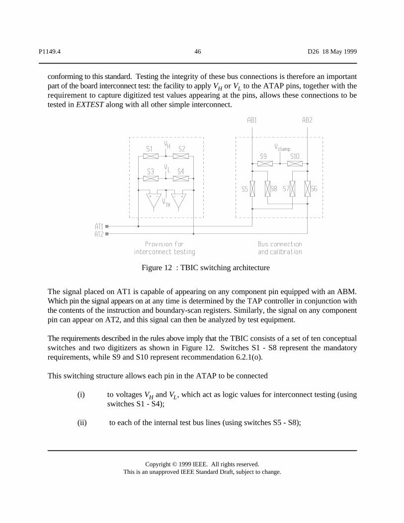
P1149.4 46 D26 18 May 1999
Copyright © 1999 IEEE. All rights reserved.This is an unapproved IEEE Standard Draft, subject to change.
Figure 12 : TBIC switching architecture
conforming to this standard. Testing the integrity of these bus connections is therefore an importantpart of the board interconnect test: the facility to apply V or V to the ATAP pins, together with theH Lrequirement to capture digitized test values appearing at the pins, allows these connections to betested in EXTEST along with all other simple interconnect.
The signal placed on AT1 is capable of appearing on any component pin equipped with an ABM.Which pin the signal appears on at any time is determined by the TAP controller in conjunction withthe contents of the instruction and boundary-scan registers. Similarly, the signal on any componentpin can appear on AT2, and this signal can then be analyzed by test equipment.
The requirements described in the rules above imply that the TBIC consists of a set of ten conceptualswitches and two digitizers as shown in Figure 12. Switches S1 - S8 represent the mandatoryrequirements, while S9 and S10 represent recommendation 6.2.1(o).
This switching structure allows each pin in the ATAP to be connected
(i) to voltages V and V , which act as logic values for interconnect testing (usingH Lswitches S1 - S4);
(ii) to each of the internal test bus lines (using switches S5 - S8);
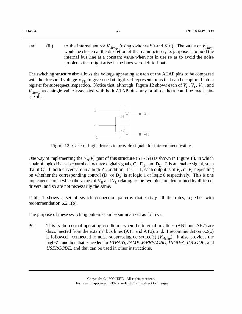
P1149.4 47 D26 18 May 1999
Copyright © 1999 IEEE. All rights reserved.This is an unapproved IEEE Standard Draft, subject to change.
Figure 13 : Use of logic drivers to provide signals for interconnect testing
and (iii) to the internal source V (using switches S9 and S10). The value of Vclamp clampwould be chosen at the discretion of the manufacturer; its purpose is to hold theinternal bus line at a constant value when not in use so as to avoid the noiseproblems that might arise if the lines were left to float.
The switching structure also allows the voltage appearing at each of the ATAP pins to be comparedwith the threshold voltage V to give one-bit digitized representations that can be captured into aTHregister for subsequent inspection. Notice that, although Figure 12 shows each of V , V , V andH L THV as a single value associated with both ATAP pins, any or all of them could be made pin-clampspecific.
One way of implementing the V /V part of this structure (S1 - S4) is shown in Figure 13, in whichH La pair of logic drivers is controlled by three digital signals, C, D , and D . C is an enable signal, such1 2that if C = 0 both drivers are in a high-Z condition. If C = 1, each output is at V or V dependingH Lon whether the corresponding control (D or D ) is at logic 1 or logic 0 respectively. This is one1 2implementation in which the values of V and V relating to the two pins are determined by differentH Ldrivers, and so are not necessarily the same.
Table 1 shows a set of switch connection patterns that satisfy all the rules, together withrecommendation 6.2.1(o).
The purpose of these switching patterns can be summarized as follows.
P0 : This is the normal operating condition, when the internal bus lines (AB1 and AB2) aredisconnected from the external bus lines (AT1 and AT2), and, if recommendation 6.2(o)is followed, connected to noise-suppressing dc source(s) (V ). It also provides theclamphigh-Z condition that is needed for BYPASS, SAMPLE/PRELOAD, HIGH-Z, IDCODE, andUSERCODE, and that can be used in other instructions.
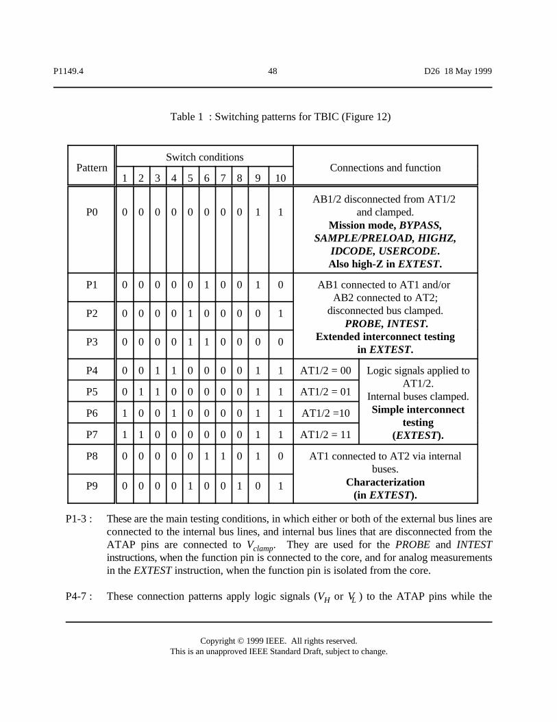
P1149.4 48 D26 18 May 1999
Copyright © 1999 IEEE. All rights reserved.This is an unapproved IEEE Standard Draft, subject to change.
PatternSwitch conditions
Connections and function1 2 3 4 5 6 7 8 9 10
P0 0 0 0 0 0 0 0 0 1 1AB1/2 disconnected from AT1/2
and clamped.Mission mode, BYPASS,
SAMPLE/PRELOAD, HIGHZ,IDCODE, USERCODE.Also high-Z in EXTEST.
P1 0 0 0 0 0 1 0 0 1 0 AB1 connected to AT1 and/or AB2 connected to AT2;
disconnected bus clamped. PROBE, INTEST.
Extended interconnect testingin EXTEST.
P2 0 0 0 0 1 0 0 0 0 1
P3 0 0 0 0 1 1 0 0 0 0
P4 0 0 1 1 0 0 0 0 1 1 AT1/2 = 00 Logic signals applied toAT1/2.
Internal buses clamped.Simple interconnect
testing(EXTEST).
P5 0 1 1 0 0 0 0 0 1 1 AT1/2 = 01
P6 1 0 0 1 0 0 0 0 1 1 AT1/2 =10
P7 1 1 0 0 0 0 0 0 1 1 AT1/2 = 11
P8 0 0 0 0 0 1 1 0 1 0 AT1 connected to AT2 via internalbuses.
Characterization(in EXTEST).
P9 0 0 0 0 1 0 0 1 0 1
Table 1 : Switching patterns for TBIC (Figure 12)
P1-3 : These are the main testing conditions, in which either or both of the external bus lines areconnected to the internal bus lines, and internal bus lines that are disconnected from theATAP pins are connected to V . They are used for the PROBE and INTESTclampinstructions, when the function pin is connected to the core, and for analog measurementsin the EXTEST instruction, when the function pin is isolated from the core.
P4-7 : These connection patterns apply logic signals (V or V ) to the ATAP pins while theH L
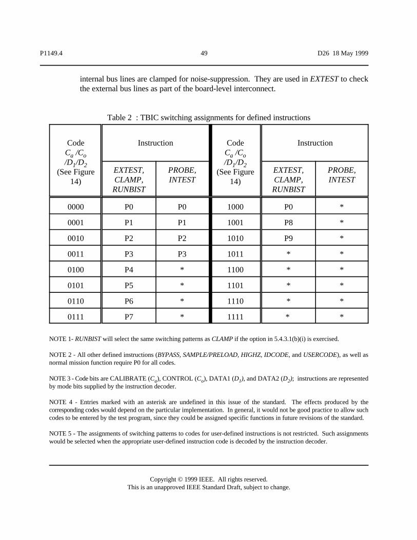
P1149.4 49 D26 18 May 1999
Copyright © 1999 IEEE. All rights reserved.This is an unapproved IEEE Standard Draft, subject to change.
CodeC /Ca o/D /D1 2
(See Figure14)
Instruction CodeC /Ca o/D /D1 2
(See Figure14)
Instruction
EXTEST,CLAMP,RUNBIST
PROBE,INTEST
EXTEST,CLAMP,RUNBIST
PROBE,INTEST
0000 P0 P0 1000 P0 *
0001 P1 P1 1001 P8 *
0010 P2 P2 1010 P9 *
0011 P3 P3 1011 * *
0100 P4 * 1100 * *
0101 P5 * 1101 * *
0110 P6 * 1110 * *
0111 P7 * 1111 * *
Table 2 : TBIC switching assignments for defined instructions
internal bus lines are clamped for noise-suppression. They are used in EXTEST to checkthe external bus lines as part of the board-level interconnect.
NOTE 1- RUNBIST will select the same switching patterns as CLAMP if the option in 5.4.3.1(b)(i) is exercised.
NOTE 2 - All other defined instructions (BYPASS, SAMPLE/PRELOAD, HIGHZ, IDCODE, and USERCODE), as well asnormal mission function require P0 for all codes.
NOTE 3 - Code bits are CALIBRATE (C ), CONTROL (C ), DATA1 (D ), and DATA2 (D ); instructions are representeda o 1 2by mode bits supplied by the instruction decoder.
NOTE 4 - Entries marked with an asterisk are undefined in this issue of the standard. The effects produced by thecorresponding codes would depend on the particular implementation. In general, it would not be good practice to allow suchcodes to be entered by the test program, since they could be assigned specific functions in future revisions of the standard.
NOTE 5 - The assignments of switching patterns to codes for user-defined instructions is not restricted. Such assignmentswould be selected when the appropriate user-defined instruction code is decoded by the instruction decoder.
P1149.4 50 D26 18 May 1999
Copyright © 1999 IEEE. All rights reserved.This is an unapproved IEEE Standard Draft, subject to change.
P8-9: These patterns are used to permit the measurement of the characteristics of the test buses(and internal switches) by applying test signals at the ATAP, passing them through AB1 orAB2, and monitoring the resulting output at the ATAP without the signal passing throughany other internal circuitry.
Additional connection patterns could be provided to support optional instructions; additional switchesmay also be fitted to increase flexibility, but the consequential effects on parasitic loading of the testbuses will need to be taken into account. These patterns will be invoked as appropriate to serve theneeds of the various instructions, as shown in Table 2.
6.3 Control of the TBIC
The TBIC consists of the switching structure (Figure 12) designed in accordance with the rules in6.2.1, together with a control circuit that allows the various connection patterns (Table 2) to beselected.
6.3.1 Specification
Rules
(a) The TBIC shall contain a control register and an update register.
(b) The control register shall consist of a shift register with four stages identified by the labelsCALIBRATE, CONTROL, DATA1, and DATA2.
(c) The control register shall form part of the boundary-scan register.
(d) The DATA1 and DATA2 stages of the control register shall capture the results of thedigitizations of the pin voltages at AT1 and AT2 respectively on the rising edge of TCKwhile the TAP controller is in the Capture-DR state.
(e) The update register shall be parallel loaded from the control register and any necessarycombinational logic in response to the falling edge of TCK while the TAP controller is inthe Update-DR state, such that serial shifting in the control register has no effect on thestate of the switches.
(f) The control circuit shall be designed to support the operating patterns shown in Table 1 andTable 2.
P1149.4 51 D26 18 May 1999
Copyright © 1999 IEEE. All rights reserved.This is an unapproved IEEE Standard Draft, subject to change.
Permissions
(g) The CALIBRATE and CONTROL stages of the control register may be used at thedesigner's discretion to capture other internal states on the rising edge of TCK while theTAP controller is in the Capture-DR state, provided that no rules of this standard areviolated.
(h) The positioning of individual stages of the control register within the boundary-scan registeris entirely at the discretion of the manufacturer.
(i) Additional switching pattern assignments may be incorporated at the manufacturer’sdiscretion to support user-defined instructions.
6.3.2 Description
One possible implementation of a TBIC controller is shown in Figure 14, which provides the controlneeded for the TBIC of Figure 12 (including the optional (recommended) switches S9 and S10), andsupports the switch connection patterns in Table 2. It should be noted that it is the designer’sresponsibility to ensure that any particular realization of a TBIC will perform correctly according tothe rules when implemented within a particular fabrication facility. It may be necessary, for example,to control the skew of the UpdateDR signal.
Because the TBIC control register is included as part of the boundary-scan register, appropriatecontrol codes can be entered serially in response to rising edges on TCK while the TAP controlleris in Shift-DR, at the same time that the boundary modules are being loaded with data.
The control signals for the individual switches are derived by the control logic from the contents ofthe update register together with a set of Mode signals, which would be supplied by the instructiondecoder. In the circuit of Figure 14, the mode signals used (Mode1 and Mode2) are those definedin Table 3, which are sufficient to support all the mandatory and optional instructions defined in IEEEStd 1149.1 and this standard. If additional user-defined instructions are supported, additional modesignals will probably need to be generated by the instruction decoder to allow the appropriate switchpatterns to be selected.
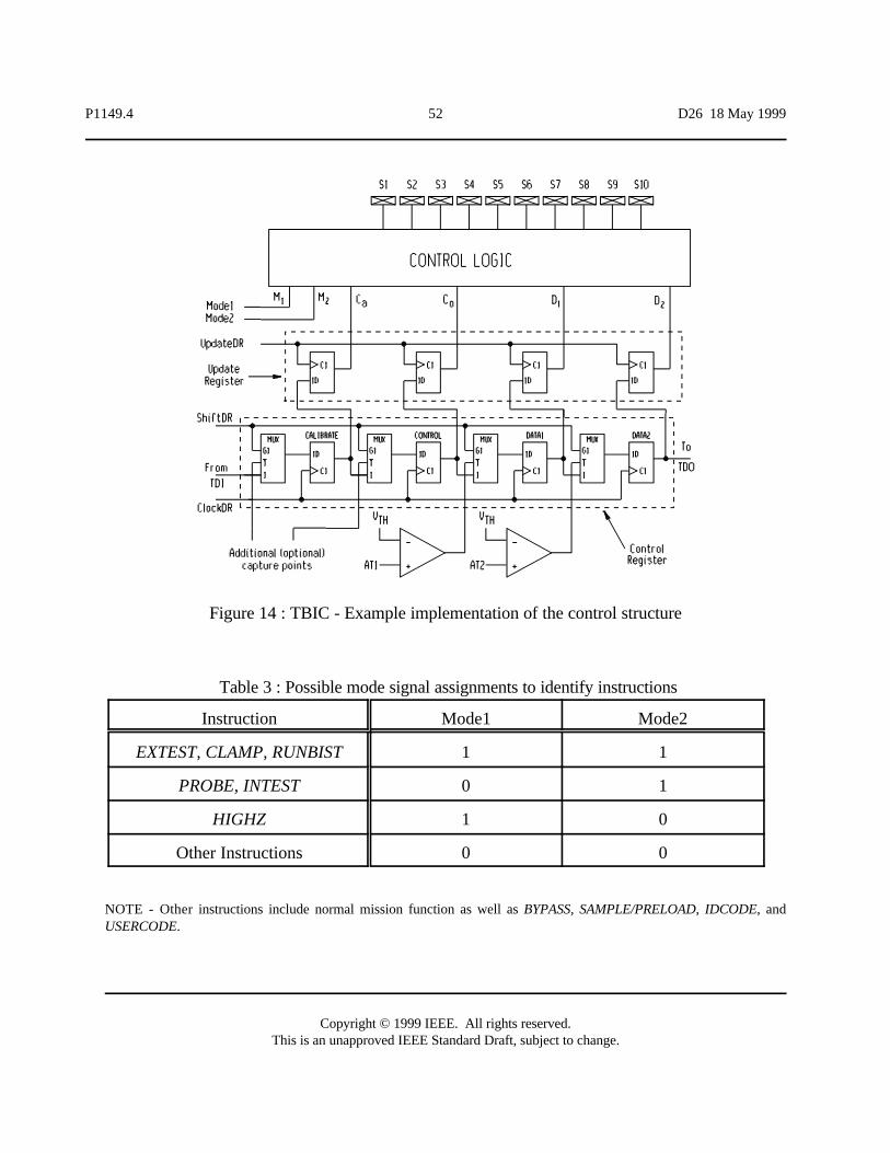
P1149.4 52 D26 18 May 1999
Copyright © 1999 IEEE. All rights reserved.This is an unapproved IEEE Standard Draft, subject to change.
Figure 14 : TBIC - Example implementation of the control structure
Instruction Mode1 Mode2
EXTEST, CLAMP, RUNBIST 1 1
PROBE, INTEST 0 1
HIGHZ 1 0
Other Instructions 0 0
Table 3 : Possible mode signal assignments to identify instructions
NOTE - Other instructions include normal mission function as well as BYPASS, SAMPLE/PRELOAD, IDCODE, andUSERCODE.

S5 ' Ca Co D1 D2 M1 M2
% Ca Co D1 D2 M1 M2
% Ca Co D1 D2 M1 M2
% Ca Co D1 D2 M1 M2
% Ca Co D1 D2 M1 M2
P1149.4 53 D26 18 May 1999
Copyright © 1999 IEEE. All rights reserved.This is an unapproved IEEE Standard Draft, subject to change.
The detailed design of the TBIC therefore requires that versions of Tables 1, 2, and 3 must first beprepared, taking into account the instructions that are to be supported (i.e., mandatory + optional +user-defined). Table 1 could include additional switching patterns for user-defined purposes; Table2 could include additional columns (for user-defined instructions) and/or could use different codingsto select the patterns; Table 3 could need additional mode signals to identify instructions and/or couldcode them differently.
To design the control logic needed (see Figure 14) to control a particular switch, it is necessary toidentify (from Table 1) which patterns require that switch to be closed. Table 2 then shows whichcodings under which instructions select those patterns, and Table 3 shows the appropriate modesignals that identify the instructions.
The procedure can be illustrated using the tables as they are (i.e., implementing a TBIC for acomponent supporting all defined instructions (mandatory and optional) but no user-definedinstructions) and finding the logic to drive switch S5. Note that in the equations the control signalfor switch SN is denoted by S , and that the code and mode bits are denoted by CALIBRATE = C ;N aCONTROL = C ; DATA1 = D ; DATA2 = D ; Mode1 = M ; Mode2 = M .o 1 2 1 2
1. From Table 1 we find that S5 is required to be closed for P2, P3, and P9.
2. From Table 2 we find that P2 is required in EXTEST, CLAMP, RUNBIST, PROBE, andINTEST for code C C D D = 0010; P3 is required in EXTEST, CLAMP, RUNBIST,a o 1 2PROBE, and INTEST for code C C D D = 0011; and P9 is required in EXTEST, CLAMP,a o 1 2and RUNBIST for code C C D D = 1010.a o 1 2
3. From Table 3 we find that the group of instructions EXTEST, CLAMP, and RUNBIST isrepresented by M M = 11, and that the group PROBE and INTEST is represented by1 2M M = 01.1 2
4. Putting these together we then get
which can be simplified to
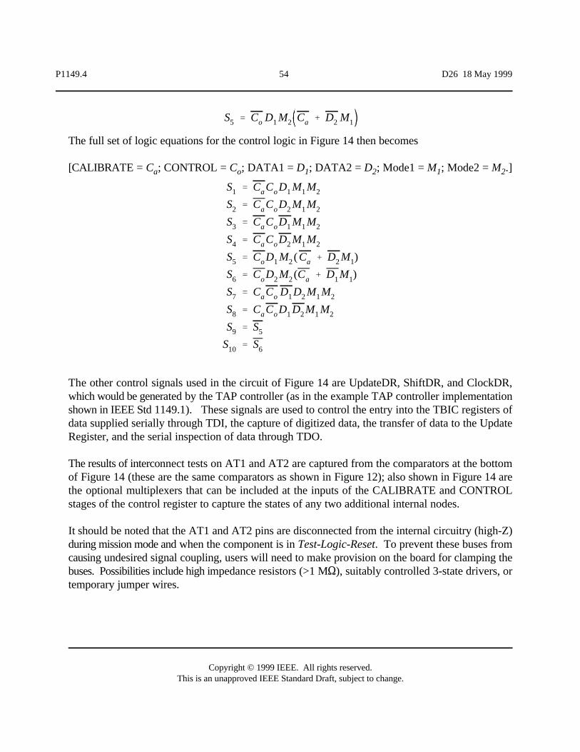
S1 ' Ca Co D1 M1 M2
S2 ' Ca Co D2 M1 M2
S3 ' Ca Co D1 M1 M2
S4 ' Ca Co D2 M1 M2
S5 ' Co D1 M2 ( Ca % D2 M1)
S6 ' Co D2 M2 (Ca % D1 M1)
S7 ' Ca Co D1 D2 M1 M2
S8 ' Ca Co D1 D2 M1 M2
S9 ' S5
S10 ' S6
S5 ' Co D1 M2 Ca % D2 M1
P1149.4 54 D26 18 May 1999
Copyright © 1999 IEEE. All rights reserved.This is an unapproved IEEE Standard Draft, subject to change.
The full set of logic equations for the control logic in Figure 14 then becomes
[CALIBRATE = C ; CONTROL = C ; DATA1 = D ; DATA2 = D ; Mode1 = M ; Mode2 = M .]a o 1 2 1 2
The other control signals used in the circuit of Figure 14 are UpdateDR, ShiftDR, and ClockDR,which would be generated by the TAP controller (as in the example TAP controller implementationshown in IEEE Std 1149.1). These signals are used to control the entry into the TBIC registers ofdata supplied serially through TDI, the capture of digitized data, the transfer of data to the UpdateRegister, and the serial inspection of data through TDO.
The results of interconnect tests on AT1 and AT2 are captured from the comparators at the bottomof Figure 14 (these are the same comparators as shown in Figure 12); also shown in Figure 14 arethe optional multiplexers that can be included at the inputs of the CALIBRATE and CONTROLstages of the control register to capture the states of any two additional internal nodes.
It should be noted that the AT1 and AT2 pins are disconnected from the internal circuitry (high-Z)during mission mode and when the component is in Test-Logic-Reset. To prevent these buses fromcausing undesired signal coupling, users will need to make provision on the board for clamping thebuses. Possibilities include high impedance resistors (>1 MS), suitably controlled 3-state drivers, ortemporary jumper wires.
P1149.4 55 D26 18 May 1999
Copyright © 1999 IEEE. All rights reserved.This is an unapproved IEEE Standard Draft, subject to change.
6.4 Differential I/O
6.4.1 Specification
Rules
(a) If additional ATAP pins (AT1N and AT2N) are provided in accordance with Permission4.3.1(d), corresponding additional internal analog test bus lines (AB1N and AB2N) shallbe provided.
(b) The additional pair of ATAP pins shall be connected to its corresponding pair of internalbus lines by a second TBIC that conforms to the rules set out in 6.2 and 6.3.
6.4.2 Description
If some of the function pins carry differential input or output signals, the manufacturer may chooseto include additional test structures to provide for differential testing, or may choose to omit theadditional structure and accept a reduced level of test function.
The optional additional structure consists of two additional pins in the ATAP (AT1N and AT2N),and two corresponding additional internal buses (AB1N and AB2N). The control of this additionalstructure is exercised by an additional TBIC, identical to that shown in Figure 12. The options withregard to boundary modules are described in 7.4, and the options with regard to test methodologiesare described in 8.1.2 and 8.1.3.
6.5 Partitioned internal test bus structure
In the simplest form of the test bus structure that has been described so far, a two-wire internal testbus will be distributed to all analog pins in the component. There are some designs (particularly thosewith multiple power supply voltages) for which this structure could lead to performance problemsbecause of cross-talk, leakage, feedback, or loading. One way of alleviating some of these problemsis to partition the internal test buses.
6.5.1 Switching
A general partitioning scheme consists of a two-pin ATAP (AT1/2) and n partitions each consistingof a pair of internal buses (AB1n and AB2n).
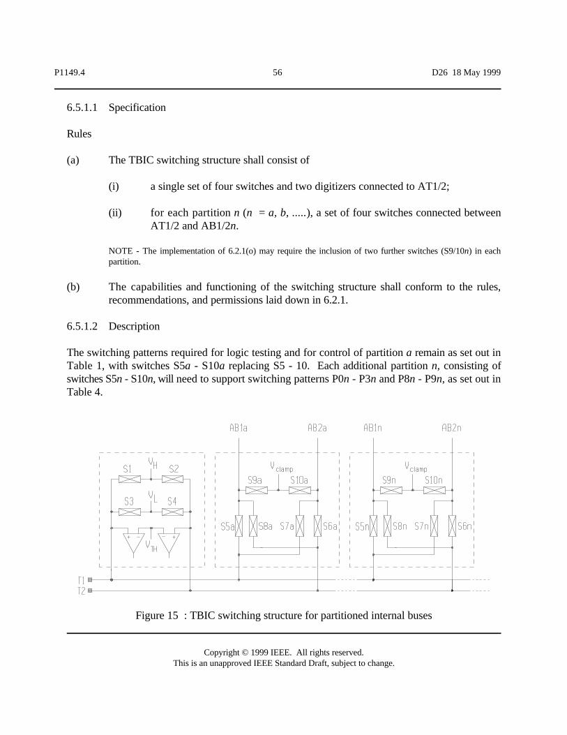
P1149.4 56 D26 18 May 1999
Copyright © 1999 IEEE. All rights reserved.This is an unapproved IEEE Standard Draft, subject to change.
Figure 15 : TBIC switching structure for partitioned internal buses
6.5.1.1 Specification
Rules
(a) The TBIC switching structure shall consist of
(i) a single set of four switches and two digitizers connected to AT1/2;
(ii) for each partition n (n = a, b, .....), a set of four switches connected betweenAT1/2 and AB1/2n.
NOTE - The implementation of 6.2.1(o) may require the inclusion of two further switches (S9/10n) in eachpartition.
(b) The capabilities and functioning of the switching structure shall conform to the rules,recommendations, and permissions laid down in 6.2.1.
6.5.1.2 Description
The switching patterns required for logic testing and for control of partition a remain as set out inTable 1, with switches S5a - S10a replacing S5 - 10. Each additional partition n, consisting ofswitches S5n - S10n, will need to support switching patterns P0n - P3n and P8n - P9n, as set out inTable 4.
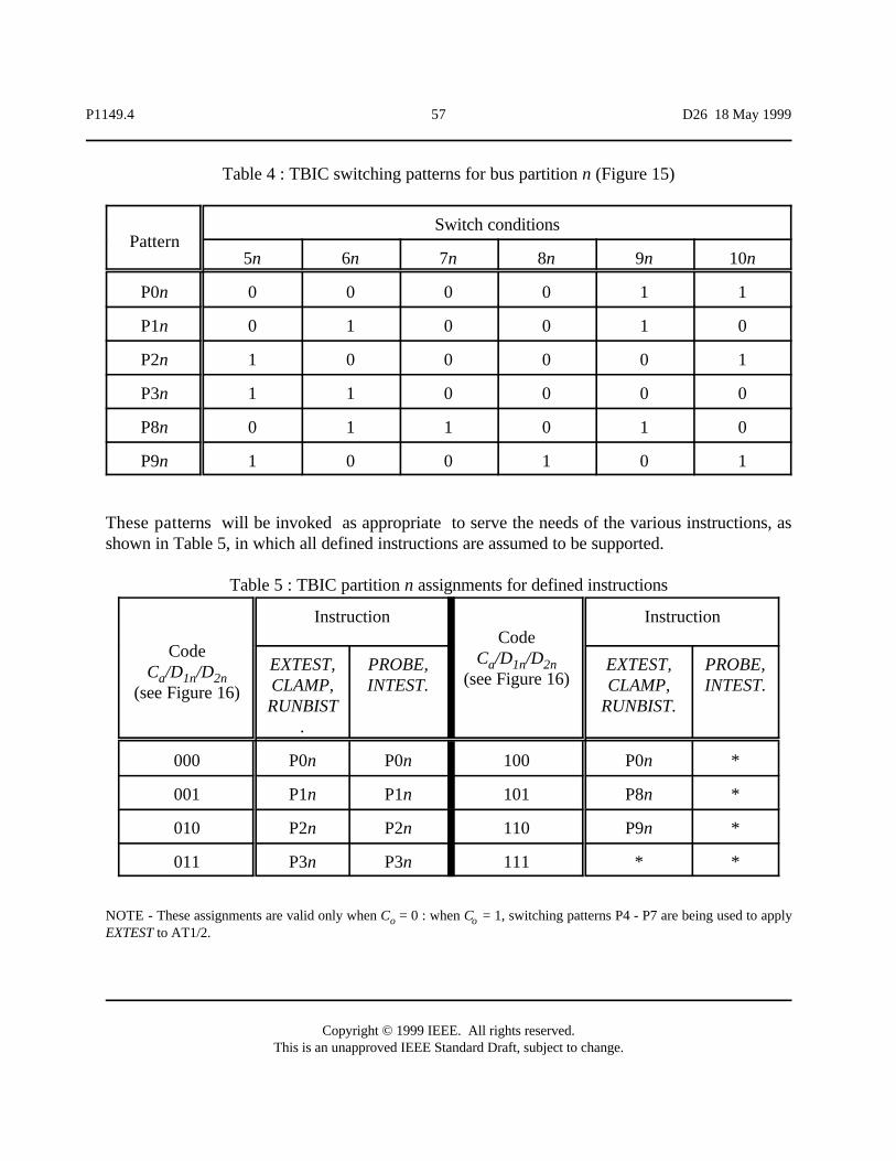
P1149.4 57 D26 18 May 1999
Copyright © 1999 IEEE. All rights reserved.This is an unapproved IEEE Standard Draft, subject to change.
PatternSwitch conditions
5n 6n 7n 8n 9n 10n
P0n 0 0 0 0 1 1
P1n 0 1 0 0 1 0
P2n 1 0 0 0 0 1
P3n 1 1 0 0 0 0
P8n 0 1 1 0 1 0
P9n 1 0 0 1 0 1
Table 4 : TBIC switching patterns for bus partition n (Figure 15)
CodeC /D /Da 1n 2n
(see Figure 16)
InstructionCode
C /D /Da 1n 2n(see Figure 16)
Instruction
EXTEST,CLAMP,RUNBIST
.
PROBE,INTEST.
EXTEST,CLAMP,
RUNBIST.
PROBE,INTEST.
000 P0n P0n 100 P0n *
001 P1n P1n 101 P8n *
010 P2n P2n 110 P9n *
011 P3n P3n 111 * *
Table 5 : TBIC partition n assignments for defined instructions
These patterns will be invoked as appropriate to serve the needs of the various instructions, asshown in Table 5, in which all defined instructions are assumed to be supported.
NOTE - These assignments are valid only when C = 0 : when C = 1, switching patterns P4 - P7 are being used to applyo oEXTEST to AT1/2.
P1149.4 58 D26 18 May 1999
Copyright © 1999 IEEE. All rights reserved.This is an unapproved IEEE Standard Draft, subject to change.
6.5.2 Control
6.5.2.1 Specification
Rules
(a) For a component whose internal test bus structure has n partitions, the TBIC shall containa control register and an update register, the structure and functioning of which (e.g., themechanism for the transfer of data through the control register, and from the controlregister to the update register) shall be identical to that of the single partition case, as laiddown in 6.3.
(b) The TBIC control and update registers shall consist of a base section together with (n - 1)extensions.
(c) The base section of the TBIC shall consist of four stages labelled CALIBRATE,CONTROL, DATA1a, and DATA2a, and the contents of these stages shall control theinterconnect test facility (switches S1 - S4 in Figure 15) and partition a (switches S5a -S10a in Figure 15). The function and performance of the base section of the TBIC shallconform to the rules laid down in 6.2.
(d) Each additional partition shall be associated with a two-bit extension to the TBIC; the bitsassociated with partition n being labelled DATA1n and DATA2n.
(e) The control register stages of the extension(s) to the TBIC shall be incorporated into theboundary-scan register.
(f) The contents of the TBIC extension, together with the contents of the CALIBRATE andCONTROL stages of the base section, shall provide the switching patterns P0n - P3nand P8n - P9n as defined in Table 4.
(g) The control circuit associated with extension n shall be designed to produce the operatingpatterns required by the instruction set (e.g.,Table 5).
Permission
(h) The DATAln and DATA2n stages of the TBIC extension may be used at the designer'sdiscretion to capture internal states on the rising edge of TCK while the TAP controller isin the Capture-DR state, provided that no rules of this standard are violated.
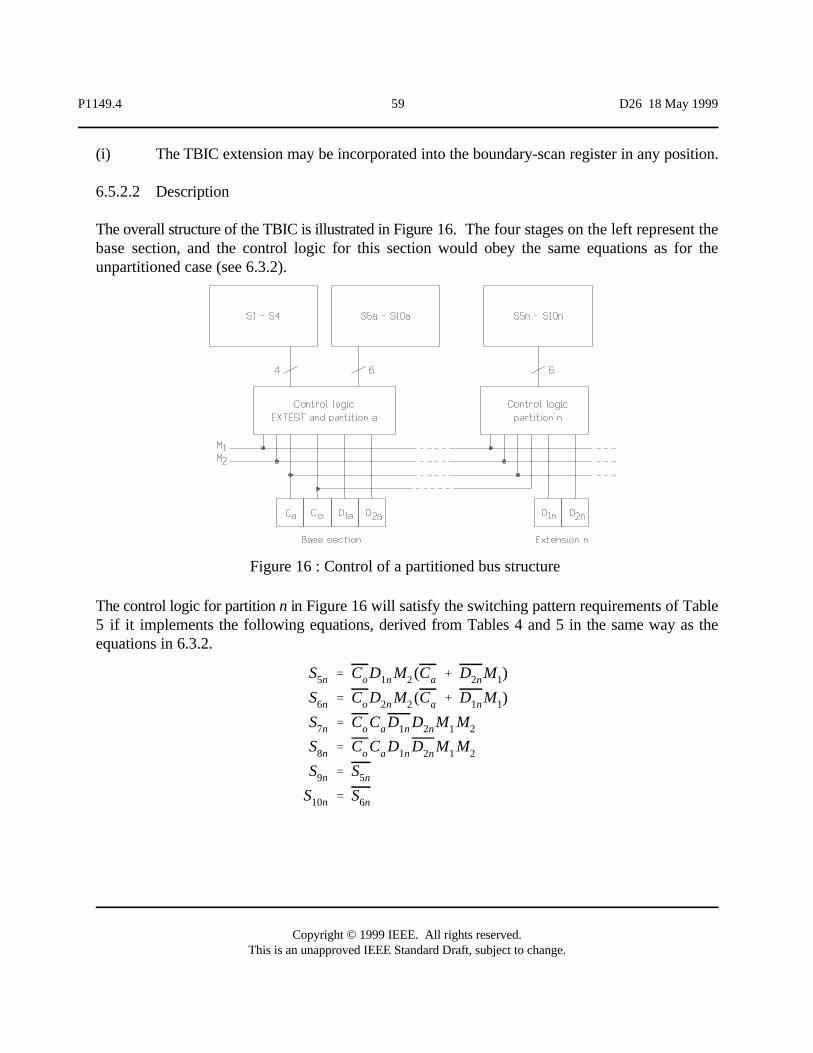
S5n ' Co D1n M2 (Ca % D2n M1)
S6n ' Co D2n M2 (Ca % D1n M1)
S7n ' Co Ca D1n D2n M1 M2
S8n ' Co Ca D1n D2n M1 M2
S9n ' S5n
S10n ' S6n
P1149.4 59 D26 18 May 1999
Copyright © 1999 IEEE. All rights reserved.This is an unapproved IEEE Standard Draft, subject to change.
Figure 16 : Control of a partitioned bus structure
(i) The TBIC extension may be incorporated into the boundary-scan register in any position.
6.5.2.2 Description
The overall structure of the TBIC is illustrated in Figure 16. The four stages on the left represent thebase section, and the control logic for this section would obey the same equations as for theunpartitioned case (see 6.3.2).
The control logic for partition n in Figure 16 will satisfy the switching pattern requirements of Table5 if it implements the following equations, derived from Tables 4 and 5 in the same way as theequations in 6.3.2.
P1149.4 60 D26 18 May 1999
Copyright © 1999 IEEE. All rights reserved.This is an unapproved IEEE Standard Draft, subject to change.
7 The Boundary-Scan Register
7.1 Structure
7.1.1 Introduction
Each function pin has associated with it a boundary module, containing one or more register stages.The boundary-scan register consists of the concatenation of register stages from each of the boundarymodules, together with the TBIC control register, into a single shift register.
The analog boundary modules (ABMs) are mixed-signal elements, in which a digital control registerdetermines the flow of analog and digital signals into and out of the analog function pins. The controlregisters in the ABMs are connected as part of the boundary-scan register.
The digital boundary modules (DBMs) (termed boundary-scan register cells in IEEE Std 1149.1) canbe of many different forms. Each DBM is a logic element contributing one or more stages to theboundary-scan register, which can be loaded serially from the TAP, or can be loaded in parallel,capturing the value being delivered at an input pin by the off-chip circuitry, or being produced at anoutput from the core. A control-and-observe DBM is one with parallel output capability; an observe-only DBM is one without parallel output capability. The distinction between these two types of DBMis important when dealing with differential I/O.
7.1.2 Specification
Rule
(a) The boundary-scan register shall consist of a concatenation of the shift register stages of allthe DBMs, the control registers of all the ABMs, and the control register(s) of the TBIC(s).
NOTE - The individual stages may be concatenated in any order.
7.1.3 Description
The boundary-scan register allows signals to be applied to the function pins without having to passthrough the core circuitry, and optionally allows signals to be applied to the core circuitry withouthaving to pass these signals in through the function pins. These signals are applied using serial digitalaccess to the boundary-scan register, and analog stimulus access to the AT1 pin. For a componentconforming to this standard, there are two forms that the boundary-scan register can take, illustrated
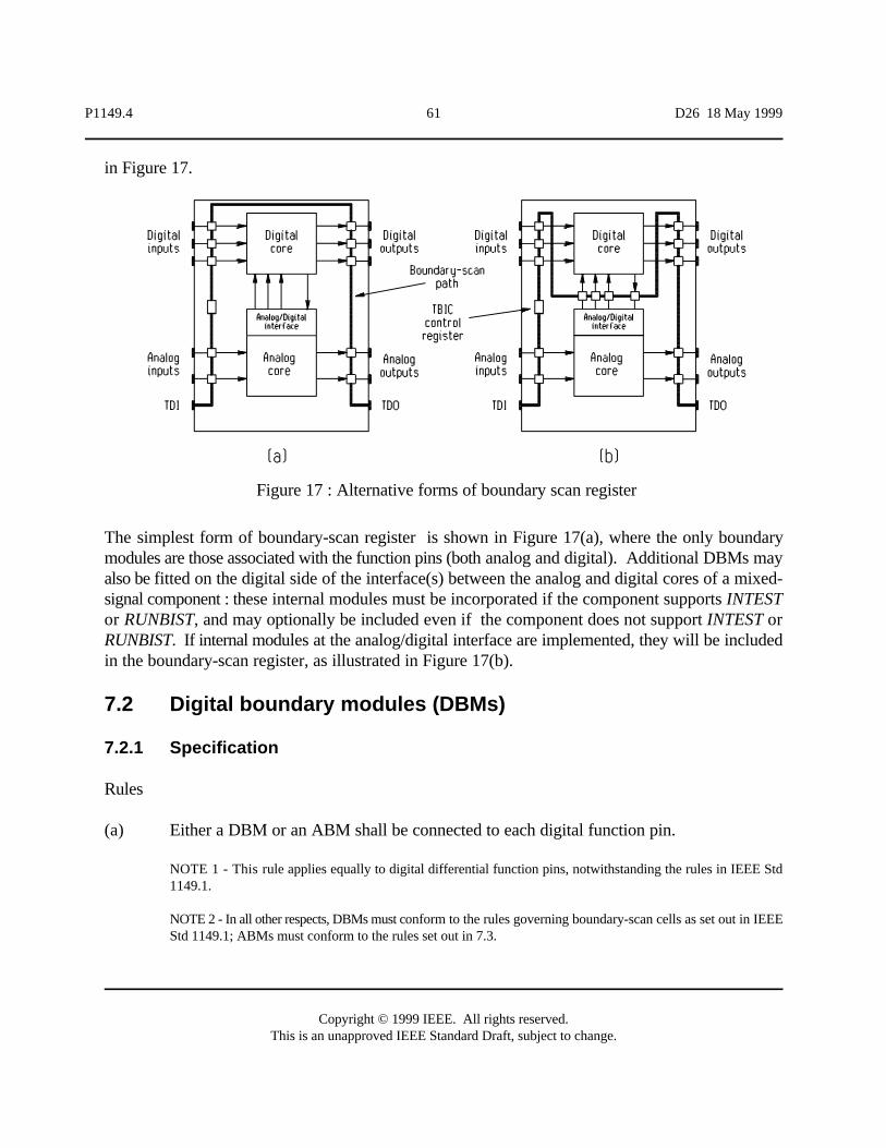
P1149.4 61 D26 18 May 1999
Copyright © 1999 IEEE. All rights reserved.This is an unapproved IEEE Standard Draft, subject to change.
Figure 17 : Alternative forms of boundary scan register
in Figure 17.
The simplest form of boundary-scan register is shown in Figure 17(a), where the only boundarymodules are those associated with the function pins (both analog and digital). Additional DBMs mayalso be fitted on the digital side of the interface(s) between the analog and digital cores of a mixed-signal component : these internal modules must be incorporated if the component supports INTESTor RUNBIST, and may optionally be included even if the component does not support INTEST orRUNBIST. If internal modules at the analog/digital interface are implemented, they will be includedin the boundary-scan register, as illustrated in Figure 17(b).
7.2 Digital boundary modules (DBMs)
7.2.1 Specification
Rules
(a) Either a DBM or an ABM shall be connected to each digital function pin.
NOTE 1 - This rule applies equally to digital differential function pins, notwithstanding the rules in IEEE Std1149.1.
NOTE 2 - In all other respects, DBMs must conform to the rules governing boundary-scan cells as set out in IEEEStd 1149.1; ABMs must conform to the rules set out in 7.3.
P1149.4 62 D26 18 May 1999
Copyright © 1999 IEEE. All rights reserved.This is an unapproved IEEE Standard Draft, subject to change.
(b) Where it is possible for the pair of output signals from a digital differential driver to be usedindependently, the two output pins shall each be connected to a control-and-observe DBM.
(c) Where it is not possible for the pair of output signals from a digital differential driver to beused independently, the two output pins shall each be connected to an observe-only DBM.
(d) Where it is not possible for the pair of output signals from a digital differential driver to beused independently, the driver input shall be connected to an observe-and-control DBM.
(e) A DBM shall be connected to the output of any digital differential receiver whose inputsare driven from function pins.
(f) If INTEST or RUNBIST is supported, a DBM shall be connected at the digital interface withon-chip analog circuitry.
NOTE - Notwithstanding the rules contained in IEEE Std 1149.1, DBMs need not be fitted at the digital interfacewith on-chip analog circuitry if neither INTEST nor RUNBIST is supported.
Recommendation
(g) Where it is possible for the pair of output signals from a digital differential driver to be usedindependently, the driver input should be connected to a DBM.
Permissions
(h) The DBMs connected at the inputs of a digital differential receiver may be either control-and-observe or observe-only.
NOTE - If control-and-observe DBMs are used, this will require a user-defined instruction to make full use of thefacilities.
(i) If a DBM is connected at the input of a digital differential driver whose outputs can be usedindependently, it may be either control-and-observe or observe-only.
NOTE - If a control-and-observe DBM is used, this will require a user-defined instruction to make full use of thefacilities.
(j) The DBM connected at the output of a digital differential receiver may be either control-and-observe or observe-only.
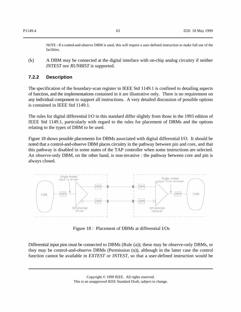
P1149.4 63 D26 18 May 1999
Copyright © 1999 IEEE. All rights reserved.This is an unapproved IEEE Standard Draft, subject to change.
Figure 18 : Placement of DBMs at differential I/Os
NOTE - If a control-and-observe DBM is used, this will require a user-defined instruction to make full use of thefacilities.
(k) A DBM may be connected at the digital interface with on-chip analog circuitry if neitherINTEST nor RUNBIST is supported.
7.2.2 Description
The specification of the boundary-scan register in IEEE Std 1149.1 is confined to detailing aspectsof function, and the implementations contained in it are illustrative only. There is no requirement onany individual component to support all instructions. A very detailed discussion of possible optionsis contained in IEEE Std 1149.1.
The rules for digital differential I/O in this standard differ slightly from those in the 1993 edition ofIEEE Std 1149.1, particularly with regard to the rules for placement of DBMs and the optionsrelating to the types of DBM to be used.
Figure 18 shows possible placements for DBMs associated with digital differential I/O. It should benoted that a control-and-observe DBM places circuitry in the pathway between pin and core, and thatthis pathway is disabled in some states of the TAP controller when some instructions are selected.An observe-only DBM, on the other hand, is non-invasive : the pathway between core and pin isalways closed.
Differential input pins must be connected to DBMs (Rule (a)); these may be observe-only DBMs, orthey may be control-and-observe DBMs (Permission (n)), although in the latter case the controlfunction cannot be available in EXTEST or INTEST, so that a user-defined instruction would be
P1149.4 64 D26 18 May 1999
Copyright © 1999 IEEE. All rights reserved.This is an unapproved IEEE Standard Draft, subject to change.
required to provide access to it. A third DBM is required to capture the signal at the output of thereceiver; this can be either observe-only or control-and-observe (Rule (e) and Permission (j)).
For differential output pins, the placement of DBMs depends on the design of the differential driver:
(i) Where it is possible to inject test control such that the output signals can be controlledindependently to either of two logic states, the output pins must be connected to control-and-observe DBMs (Rule (b)). This provides the highest degree of controllability andconsequent test coverage. It also ensures testability of board-level interconnections whereone of the output signals from a pair is used to drive a single-ended input pin on anothercomponent. Optionally, a third DBM, which can be either observe-only or control-and-observe, may be provided at the input to the differential driver (Recommendation (g) andPermission (i)). Again the the use of a control-and-observe DBM would require a user-defined instruction : in this case, the facility would be used to control the differential driverfrom its single-ended input to allow test control of the signal when the differential signalingis required for proper transmission.
(ii) Where such control is not possible (i.e., the signals are always, in test and function modes,inherently driven to opposing states), three DBMs must be provided for each differentialdriver. In addition to two observe-only DBMs at the output pins, a control-and-observeDBM must be provided at the driver input (Rules (c) and (d)).
Permission (k) allows the incorporation of test structures to test on-chip ADCs and DACs.
Fitting an ABM rather than a DBM at a particular digital output pin allows the designer to takeadvantage of the analog test features provided by this standard so that (e.g.) pull-up resistors on buslines can be measured. The use of this Permission effectively requires the designer to regard the digitalpin as though it were analog, and to attach to it an ABM, complete with its four-bit control andupdate registers (see 7.3).
7.3 Analog boundary modules (ABMs)
7.3.1 Specification
Rules
(a) An ABM shall be connected to each analog function pin.
NOTE 1 - This rule applies notwithstanding the provisions of IEEE Std 1149.1, in which boundary modules on
VH % VL
2±
VH & VL
4
P1149.4 65 D26 18 May 1999
Copyright © 1999 IEEE. All rights reserved.This is an unapproved IEEE Standard Draft, subject to change.
analog pins are forbidden.
NOTE 2 - The ABMs attached to differential pins are subject to additional rules (see 7.4).
(b) Each ABM shall be designed with a “core disconnect” facility.
NOTE 1 - Core disconnect is intended to allow the pin to be effectively isolated from all internal ac and dc sources,and to allow it to be driven externally without adversely affecting the core circuitry. When this facility is invoked,the pin is said to be in the CD state.
NOTE 2 - The most straightforward way of satisfying this rule is to include a conceptual switch between the pinand the core. The core disconnect facility may, in many cases, be integrated into the core circuitry.
(c) The ABM shall be designed so that the pin is capable of being connected to neither, eitheror both of two internal analog test bus lines.
NOTE 1 - The two test bus lines shall be AB1 and AB2 except when additional analog test bus lines are suppliedfor differential stimulus and/or measurements (see 6.4), or when the internal bus lines are partitioned (see 6.5).
NOTE 2 - When additional analog test bus lines are supplied for differential stimulus and/or measurements (see6.4), an ABM attached to a positive input or output shall be associated with AB1 and AB2, while an ABMattached to a negative input or output shall be associated with AB1N and AB2N.
(d) The ABM shall be capable of transmitting current received from AB1 through its functionpin to an external circuit.
(e) The ABM shall be capable of transmitting to AB2 the voltage appearing on its function pin.
(f) The ABM shall be capable of monitoring a one-bit digital representation of the voltageappearing at the pin. The pin voltage is to be digitized with respect to a voltage VTH(conceptual or actual) whose value lies in the range
NOTE - The choice of V in this case is subject to the same conditions as expressed in the notes attached to ruleTH6.2.1(l).
(g) The ABM shall be designed so that the pin is capable of delivering either of two voltagelevels (V or V ) to the external circuitry.H L
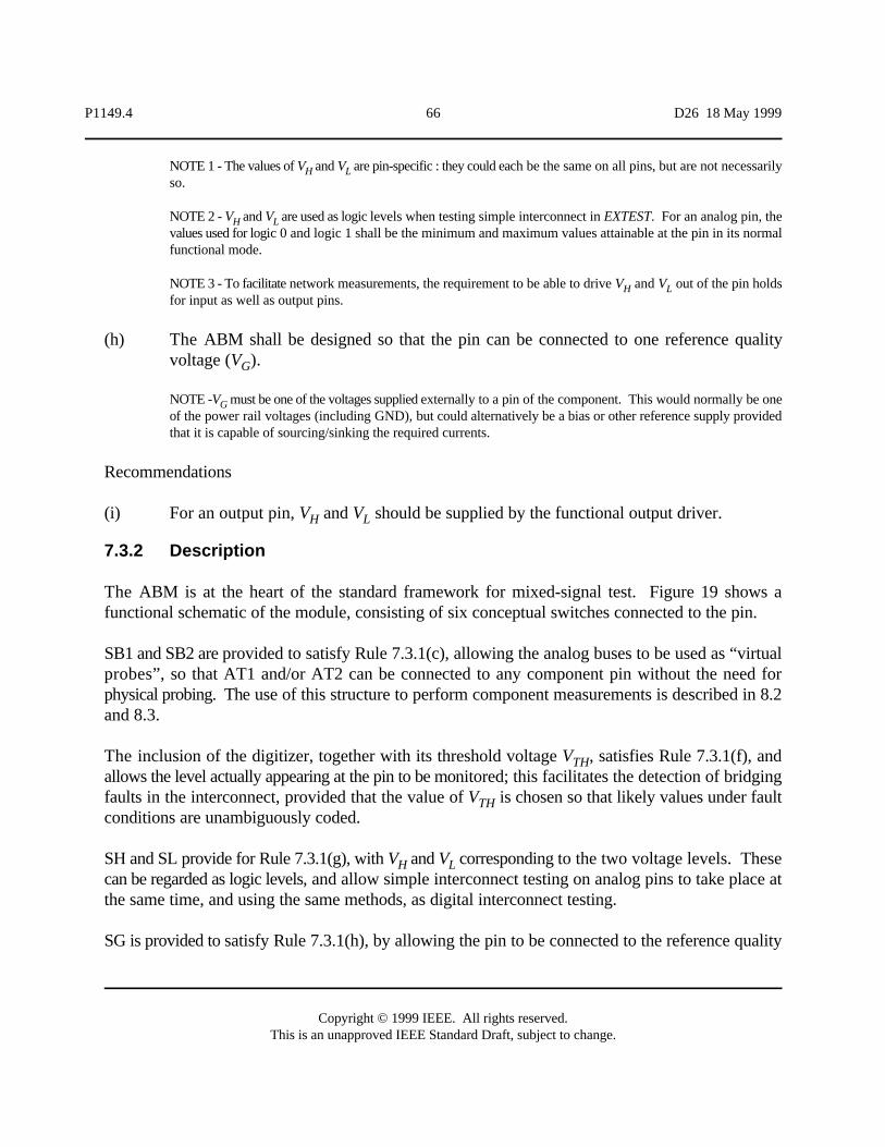
P1149.4 66 D26 18 May 1999
Copyright © 1999 IEEE. All rights reserved.This is an unapproved IEEE Standard Draft, subject to change.
NOTE 1 - The values of V and V are pin-specific : they could each be the same on all pins, but are not necessarilyH Lso.
NOTE 2 - V and V are used as logic levels when testing simple interconnect in EXTEST. For an analog pin, theH Lvalues used for logic 0 and logic 1 shall be the minimum and maximum values attainable at the pin in its normalfunctional mode.
NOTE 3 - To facilitate network measurements, the requirement to be able to drive V and V out of the pin holdsH Lfor input as well as output pins.
(h) The ABM shall be designed so that the pin can be connected to one reference qualityvoltage (V ).G
NOTE -V must be one of the voltages supplied externally to a pin of the component. This would normally be oneGof the power rail voltages (including GND), but could alternatively be a bias or other reference supply providedthat it is capable of sourcing/sinking the required currents.
Recommendations
(i) For an output pin, V and V should be supplied by the functional output driver.H L
7.3.2 Description
The ABM is at the heart of the standard framework for mixed-signal test. Figure 19 shows afunctional schematic of the module, consisting of six conceptual switches connected to the pin.
SB1 and SB2 are provided to satisfy Rule 7.3.1(c), allowing the analog buses to be used as “virtualprobes”, so that AT1 and/or AT2 can be connected to any component pin without the need forphysical probing. The use of this structure to perform component measurements is described in 8.2and 8.3.
The inclusion of the digitizer, together with its threshold voltage V , satisfies Rule 7.3.1(f), andTHallows the level actually appearing at the pin to be monitored; this facilitates the detection of bridgingfaults in the interconnect, provided that the value of V is chosen so that likely values under faultTHconditions are unambiguously coded.
SH and SL provide for Rule 7.3.1(g), with V and V corresponding to the two voltage levels. TheseH Lcan be regarded as logic levels, and allow simple interconnect testing on analog pins to take place atthe same time, and using the same methods, as digital interconnect testing.
SG is provided to satisfy Rule 7.3.1(h), by allowing the pin to be connected to the reference quality
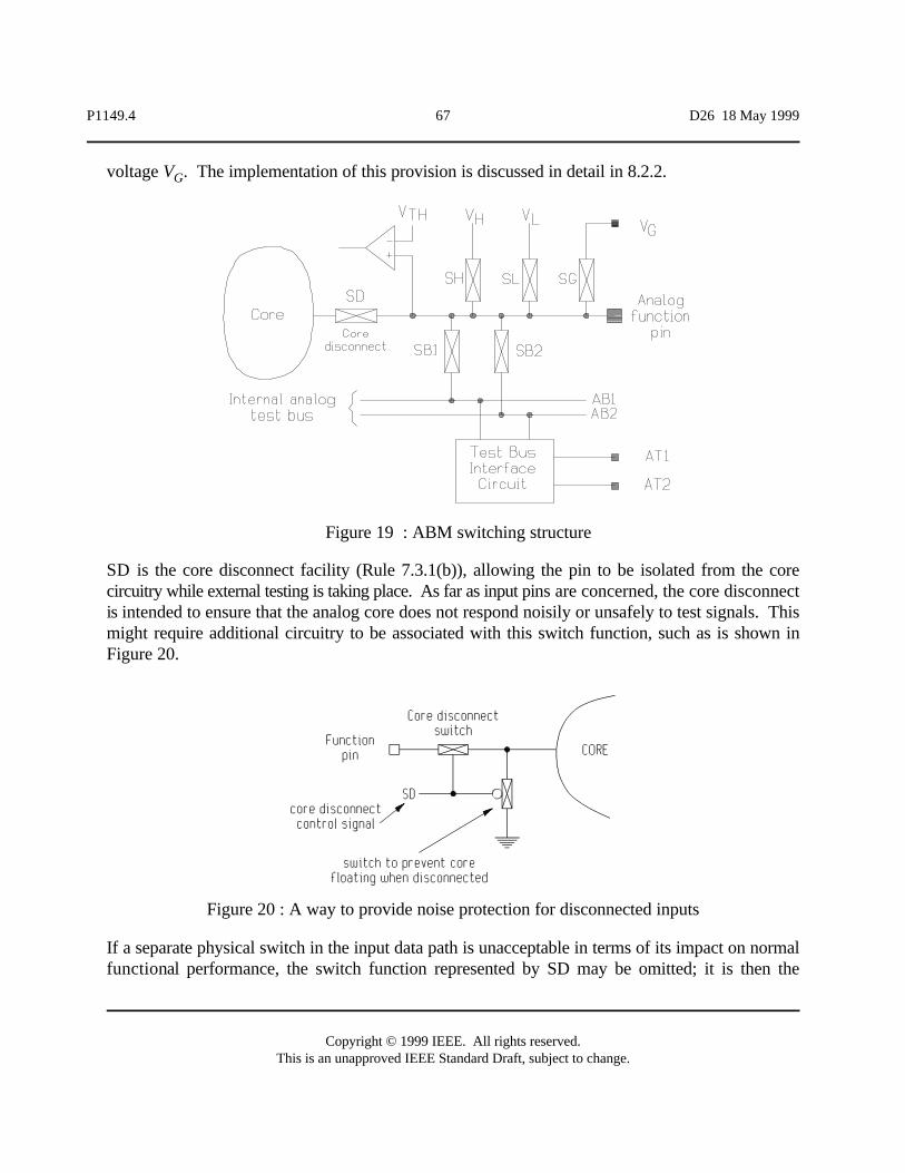
P1149.4 67 D26 18 May 1999
Copyright © 1999 IEEE. All rights reserved.This is an unapproved IEEE Standard Draft, subject to change.
Figure 19 : ABM switching structure
Figure 20 : A way to provide noise protection for disconnected inputs
voltage V . The implementation of this provision is discussed in detail in 8.2.2.G
SD is the core disconnect facility (Rule 7.3.1(b)), allowing the pin to be isolated from the corecircuitry while external testing is taking place. As far as input pins are concerned, the core disconnectis intended to ensure that the analog core does not respond noisily or unsafely to test signals. Thismight require additional circuitry to be associated with this switch function, such as is shown inFigure 20.
If a separate physical switch in the input data path is unacceptable in terms of its impact on normalfunctional performance, the switch function represented by SD may be omitted; it is then the
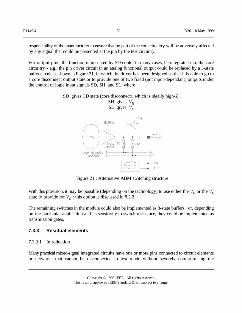
P1149.4 68 D26 18 May 1999
Copyright © 1999 IEEE. All rights reserved.This is an unapproved IEEE Standard Draft, subject to change.
Figure 21 : Alternative ABM switching structure
responsibility of the manufacturer to ensure that no part of the core circuitry will be adversely affectedby any signal that could be presented at the pin by the test circuitry.
For output pins, the function represented by SD could, in many cases, be integrated into the corecircuitry - e.g., the pin driver circuit in an analog functional output could be replaced by a 3-statebuffer circuit, as shown in Figure 21, in which the driver has been designed so that it is able to go toa core disconnect output state or to provide one of two fixed (not input-dependant) outputs underthe control of logic input signals SD, SH, and SL, where
SD gives CD state (core disconnect), which is ideally high-Z SH gives VHSL gives VL
With this provision, it may be possible (depending on the technology) to use either the V or the VH Lstate to provide for V : this option is discussed in 8.2.2.G
The remaining switches in the module could also be implemented as 3-state buffers, or, dependingon the particular application and its sensitivity to switch resistance, they could be implemented astransmission gates.
7.3.3 Residual elements
7.3.3.1 Introduction
Many practical mixed-signal integrated circuits have one or more pins connected to circuit elementsor networks that cannot be disconnected in test mode without severely compromising the
P1149.4 69 D26 18 May 1999
Copyright © 1999 IEEE. All rights reserved.This is an unapproved IEEE Standard Draft, subject to change.
component’s performance in mission mode. Examples are :
C A line driver may have an on-chip 50 S termination resistor. To disconnect this wouldrequire a switch that could add unacceptable capacitance.
C High precision circuits may contain resistors connected directly to a pin for accuracy ormatching reasons. A series switch could result in unacceptable mismatch or non-linearity.
In such cases, the core circuitry, which is isolated from the pin by the core disconnect switch, isconsidered to exclude these “residual elements”, which remain permanently connected to the pin. Theterm 'CD state' is used to indicate that the pin is effectively disconnected from the core but is notnecessarily in the high-impedance state. Provided the residual elements are restricted in type andconnectivity, the measurements made in test mode can be corrected to allow for their effects.
7.3.3.2 Specification of residual elements
Rules
(a) If any circuitry cannot be isolated from the function pins in test mode, it shall be capable ofbeing modeled as a network of residual elements.
(b) Residual elements shall consist exclusively of linear passive components (resistors,capacitors, and inductors) together with independent dc voltage and current sources.
(c) If one end of a residual element is connected to an analog function pin, the other end shallbe connected either to another analog function pin, or to a power supply pin, or to otherresidual elements.
NOTE - Reference supply pins are considered to be analog function pins.
(d) If one end of a residual element is connected to a digital function pin, the other end shall beconnected to a power supply pin.
(e) Residual elements shall not connect to the core circuitry.
(f) All residual elements shall be documented.
NOTE - The documentation required for residual elements is detailed in Clause 10, which also specifies the wayin which it must be presented.
P1149.4 70 D26 18 May 1999
Copyright © 1999 IEEE. All rights reserved.This is an unapproved IEEE Standard Draft, subject to change.
Recommendation
(g) The use of residual elements should be avoided as far as possible without compromisingmission function or performance.
Permission
(h) The residual element network may contain networks or devices whose model in terms oflinear networks (as in 7.3.3.2(b) above) is valid only over a specified range of pin currentsand voltages.
7.3.3.3 Description
Ideally, every pin, both input and output, would have the facility to be completely isolated from theinternal circuitry while the component is in test mode : in other words, there would be coredisconnect on every pin and there would be no residual components. The pins would then be drivenby test signals applied through the ABM without either being influenced by signals from the corecircuitry or injecting signals into the core circuitry. Allowing residual elements on output pins, andallowing input pins not to be equipped with core disconnect, are relaxations from the ideal that shouldbe applied only when it is essential for operational reasons.
If residual elements are to be included in the component, it is important that their effects can becalculated so that measurements can be corrected and accuracy maintained. For this reason, residualelements must be documented (see 10.3), and they are restricted to linear networks : controlledsources are disallowed, since they are often particularly sensitive to measurement errors (small offsetscan be multiplied and propagated through the system). It is, however, permitted for the residual“element” to take the form of a network rather than just a single element, provided that it can bemodelled, over an appropriate range of current and voltage, as a network of linear passive elementsand independent dc sources.
As well as restricting the types of permitted residual elements, the rules also restrict the connectivity.
Figure 22 illustrates some of the permitted and forbidden connections, with respect to a componentwith three analog pins, F1 - F3, one digital pin, F4, and a power supply pin, V . The CD switchSSbetween each analog pin and the core is shown, but the rest of the (standard) ABM is omitted forclarity. Each of the seven elements, E1 - E7, represents a passive element or an independent dcsource.
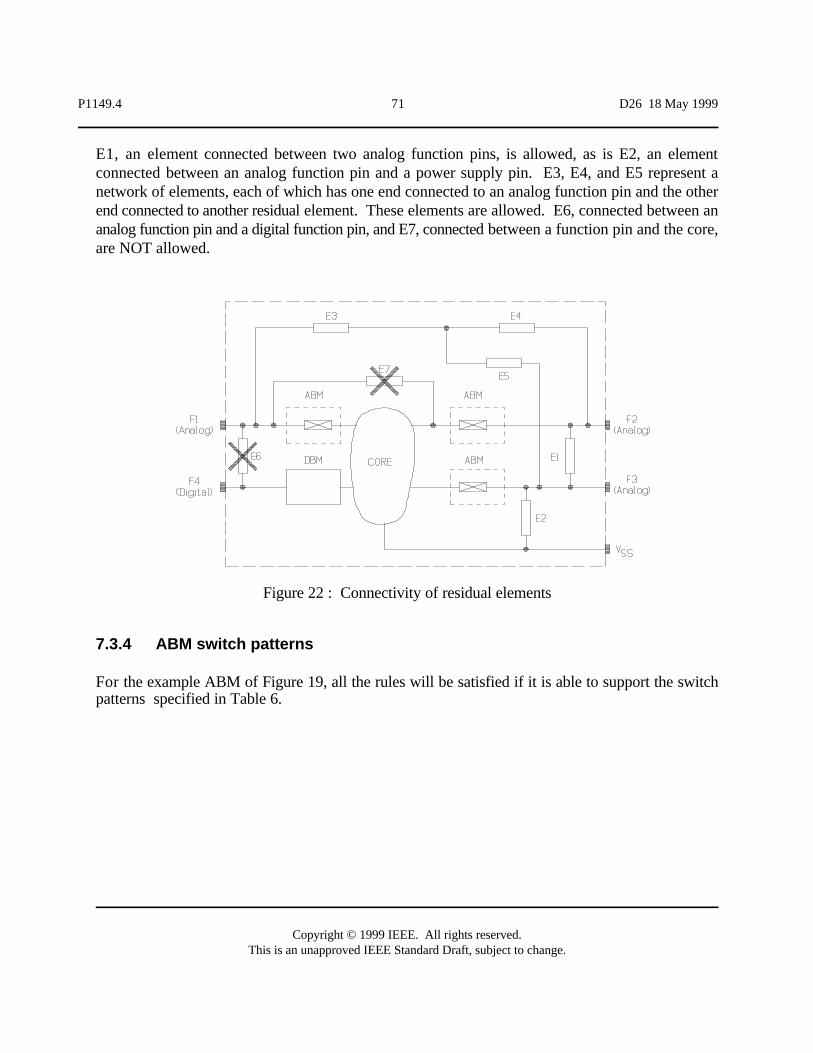
P1149.4 71 D26 18 May 1999
Copyright © 1999 IEEE. All rights reserved.This is an unapproved IEEE Standard Draft, subject to change.
Figure 22 : Connectivity of residual elements
E1, an element connected between two analog function pins, is allowed, as is E2, an elementconnected between an analog function pin and a power supply pin. E3, E4, and E5 represent anetwork of elements, each of which has one end connected to an analog function pin and the otherend connected to another residual element. These elements are allowed. E6, connected between ananalog function pin and a digital function pin, and E7, connected between a function pin and the core,are NOT allowed.
7.3.4 ABM switch patterns
For the example ABM of Figure 19, all the rules will be satisfied if it is able to support the switchpatterns specified in Table 6.
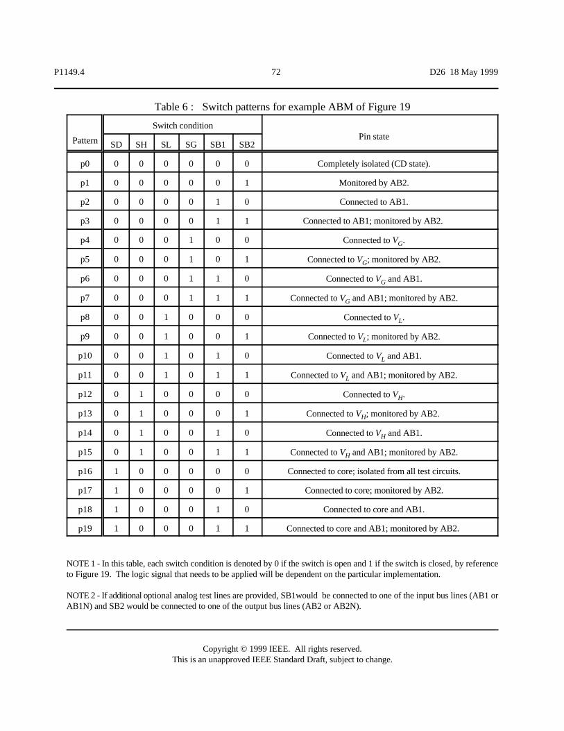
P1149.4 72 D26 18 May 1999
Copyright © 1999 IEEE. All rights reserved.This is an unapproved IEEE Standard Draft, subject to change.
Pattern
Switch conditionPin state
SD SH SL SG SB1 SB2
p0 0 0 0 0 0 0 Completely isolated (CD state).
p1 0 0 0 0 0 1 Monitored by AB2.
p2 0 0 0 0 1 0 Connected to AB1.
p3 0 0 0 0 1 1 Connected to AB1; monitored by AB2.
p4 0 0 0 1 0 0 Connected to V .G
p5 0 0 0 1 0 1 Connected to V ; monitored by AB2.G
p6 0 0 0 1 1 0 Connected to V and AB1.G
p7 0 0 0 1 1 1 Connected to V and AB1; monitored by AB2.G
p8 0 0 1 0 0 0 Connected to V .L
p9 0 0 1 0 0 1 Connected to V ; monitored by AB2.L
p10 0 0 1 0 1 0 Connected to V and AB1.L
p11 0 0 1 0 1 1 Connected to V and AB1; monitored by AB2.L
p12 0 1 0 0 0 0 Connected to V .H
p13 0 1 0 0 0 1 Connected to V ; monitored by AB2. H
p14 0 1 0 0 1 0 Connected to V and AB1.H
p15 0 1 0 0 1 1 Connected to V and AB1; monitored by AB2.H
p16 1 0 0 0 0 0 Connected to core; isolated from all test circuits.
p17 1 0 0 0 0 1 Connected to core; monitored by AB2.
p18 1 0 0 0 1 0 Connected to core and AB1.
p19 1 0 0 0 1 1 Connected to core and AB1; monitored by AB2.
Table 6 : Switch patterns for example ABM of Figure 19
NOTE 1 - In this table, each switch condition is denoted by 0 if the switch is open and 1 if the switch is closed, by referenceto Figure 19. The logic signal that needs to be applied will be dependent on the particular implementation.
NOTE 2 - If additional optional analog test lines are provided, SB1would be connected to one of the input bus lines (AB1 orAB1N) and SB2 would be connected to one of the output bus lines (AB2 or AB2N).
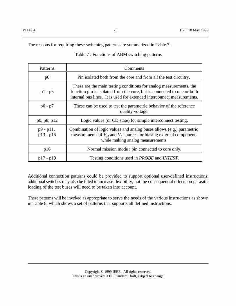
P1149.4 73 D26 18 May 1999
Copyright © 1999 IEEE. All rights reserved.This is an unapproved IEEE Standard Draft, subject to change.
Patterns Comments
p0 Pin isolated both from the core and from all the test circuitry.
p1 - p5These are the main testing conditions for analog measurements, the
function pin is isolated from the core, but is connected to one or bothinternal bus lines. It is used for extended interconnect measurements.
p6 - p7 These can be used to test the parametric behavior of the referencequality voltage.
p0, p8, p12 Logic values (or CD state) for simple interconnect testing.
p9 - p11, p13 - p15
Combination of logic values and analog buses allows (e.g.) parametric measurements of V and V sources, or biasing external componentsH L
while making analog measurements.
p16 Normal mission mode : pin connected to core only.
p17 - p19 Testing conditions used in PROBE and INTEST.
Table 7 : Functions of ABM switching patterns
The reasons for requiring these switching patterns are summarized in Table 7.
Additional connection patterns could be provided to support optional user-defined instructions;additional switches may also be fitted to increase flexibility, but the consequential effects on parasiticloading of the test buses will need to be taken into account.
These patterns will be invoked as appropriate to serve the needs of the various instructions as shownin Table 8, which shows a set of patterns that supports all defined instructions.
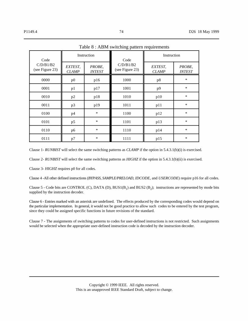
P1149.4 74 D26 18 May 1999
Copyright © 1999 IEEE. All rights reserved.This is an unapproved IEEE Standard Draft, subject to change.
CodeC/D/B1/B2
(see Figure 23)
InstructionCode
C/D/B1/B2(see Figure 23)
Instruction
EXTEST,CLAMP
PROBE,INTEST
EXTEST,CLAMP
PROBE,INTEST
0000 p0 p16 1000 p8 *
0001 p1 p17 1001 p9 *
0010 p2 p18 1010 p10 *
0011 p3 p19 1011 p11 *
0100 p4 * 1100 p12 *
0101 p5 * 1101 p13 *
0110 p6 * 1110 p14 *
0111 p7 * 1111 p15 *
Table 8 : ABM switching pattern requirements
Clause 1- RUNBIST will select the same switching patterns as CLAMP if the option in 5.4.3.1(b)(i) is exercised.
Clause 2- RUNBIST will select the same switching patterns as HIGHZ if the option in 5.4.3.1(b)(ii) is exercised.
Clause 3- HIGHZ requires p0 for all codes.
Clause 4 -All other defined instructions (BYPASS, SAMPLE/PRELOAD, IDCODE, and USERCODE) require p16 for all codes.
Clause 5 - Code bits are CONTROL (C), DATA (D), BUS1(B ) and BUS2 (B ); instructions are represented by mode bits1 2supplied by the instruction decoder.
Clause 6 - Entries marked with an asterisk are undefined. The effects produced by the corresponding codes would depend onthe particular implementation. In general, it would not be good practice to allow such codes to be entered by the test program,since they could be assigned specific functions in future revisions of the standard.
Clause 7 - The assignments of switching patterns to codes for user-defined instructions is not restricted. Such assignmentswould be selected when the appropriate user-defined instruction code is decoded by the instruction decoder.
P1149.4 75 D26 18 May 1999
Copyright © 1999 IEEE. All rights reserved.This is an unapproved IEEE Standard Draft, subject to change.
7.3.5 Control of the ABM
7.3.5.1 Specification
Rules
(a) Each ABM shall contain a control register and an update register.
(b) The control register shall consist of four stages, identified by the labels BUS1, BUS2,CONTROL, and DATA.
(c) The control register shall form part of the boundary-scan register.
(d) The update register shall be parallel loaded from the control register and any necessarycombinational logic in response to the falling edge of TCK while the TAP controller is inthe Update-DR state.
(e) The control circuitry of the ABM shall be designed so that the contents of the updateregister together with signals derived from the TAP controller and the instruction decoderallow operation in accordance with the operating modes specified in 7.3.4, Table 6 andTable 8.
(f) The result of the digitization of the pin voltage shall be captured in the DATA stage of thecontrol register on the rising edge of TCK while the TAP controller is in the Capture-DRstate.
Permissions
(g) Other stages of the ABM control register may be used at the designer's discretion to captureinternal states on a rising edge of TCK while the TAP controller is in the Capture-DR state,provided that no rules of this standard are violated.
NOTE - Values captured into the control register could be transferred into the update register with unforseenconsequences if particular sequences of TAP controller states are executed (e.g., CAPTURE-DR, EXIT1-DR,UPDATE-DR).
(h) When the control register stages are incorporated into the boundary-scan register, they maybe grouped and ordered in any way to suit the convenience of the manufacturer.
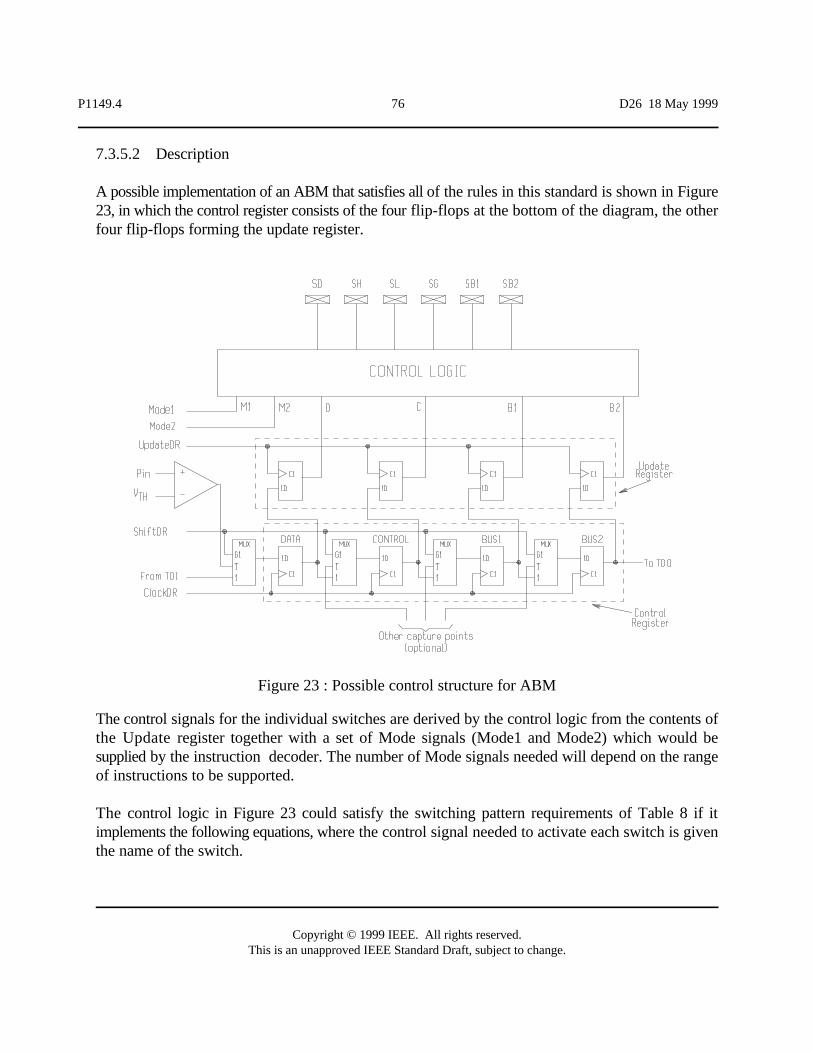
P1149.4 76 D26 18 May 1999
Copyright © 1999 IEEE. All rights reserved.This is an unapproved IEEE Standard Draft, subject to change.
Figure 23 : Possible control structure for ABM
7.3.5.2 Description
A possible implementation of an ABM that satisfies all of the rules in this standard is shown in Figure23, in which the control register consists of the four flip-flops at the bottom of the diagram, the otherfour flip-flops forming the update register.
The control signals for the individual switches are derived by the control logic from the contents ofthe Update register together with a set of Mode signals (Mode1 and Mode2) which would besupplied by the instruction decoder. The number of Mode signals needed will depend on the rangeof instructions to be supported.
The control logic in Figure 23 could satisfy the switching pattern requirements of Table 8 if itimplements the following equations, where the control signal needed to activate each switch is giventhe name of the switch.
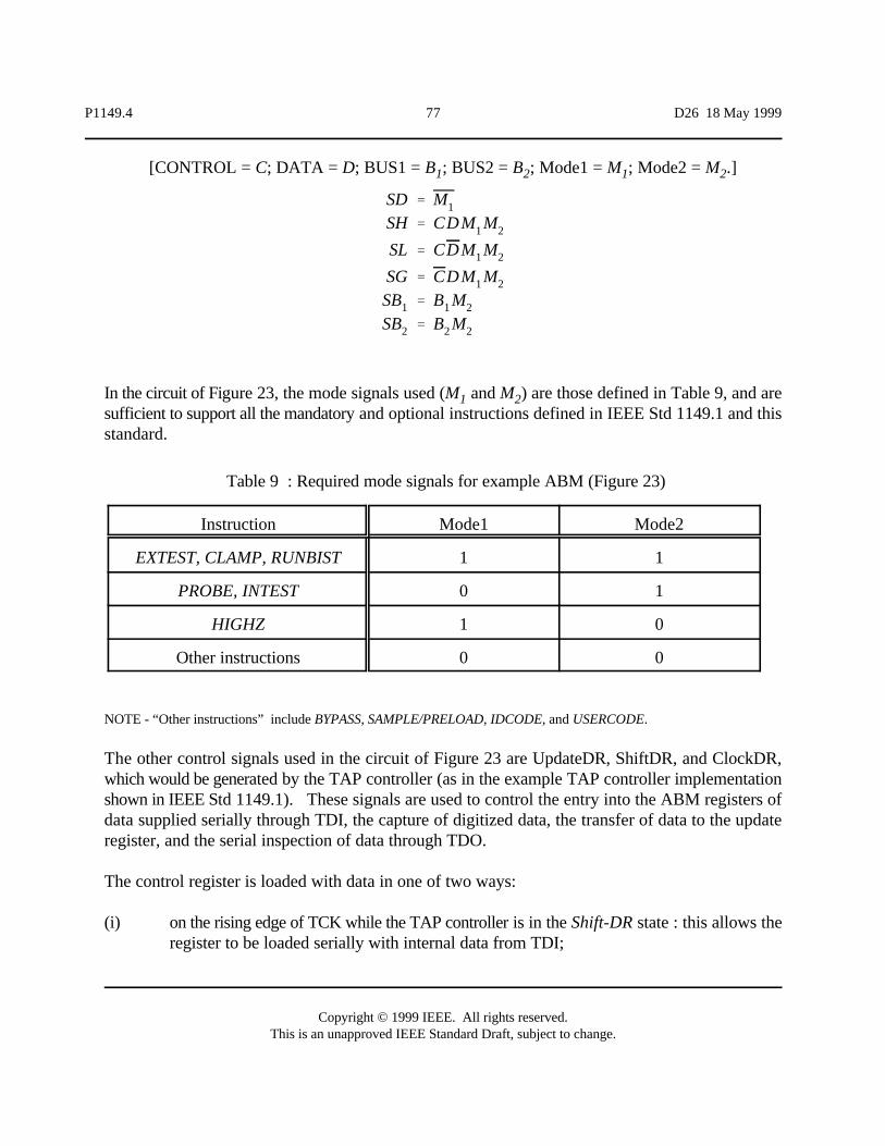
SD ' M1
SH ' CDM1 M2
SL ' CDM1 M2
SG ' CDM1 M2
SB1 ' B1 M2
SB2 ' B2 M2
P1149.4 77 D26 18 May 1999
Copyright © 1999 IEEE. All rights reserved.This is an unapproved IEEE Standard Draft, subject to change.
Instruction Mode1 Mode2
EXTEST, CLAMP, RUNBIST 1 1
PROBE, INTEST 0 1
HIGHZ 1 0
Other instructions 0 0
Table 9 : Required mode signals for example ABM (Figure 23)
[CONTROL = C; DATA = D; BUS1 = B ; BUS2 = B ; Mode1 = M ; Mode2 = M .]1 2 1 2
In the circuit of Figure 23, the mode signals used (M and M ) are those defined in Table 9, and are1 2sufficient to support all the mandatory and optional instructions defined in IEEE Std 1149.1 and thisstandard.
NOTE - “Other instructions” include BYPASS, SAMPLE/PRELOAD, IDCODE, and USERCODE.
The other control signals used in the circuit of Figure 23 are UpdateDR, ShiftDR, and ClockDR,which would be generated by the TAP controller (as in the example TAP controller implementationshown in IEEE Std 1149.1). These signals are used to control the entry into the ABM registers ofdata supplied serially through TDI, the capture of digitized data, the transfer of data to the updateregister, and the serial inspection of data through TDO.
The control register is loaded with data in one of two ways:
(i) on the rising edge of TCK while the TAP controller is in the Shift-DR state : this allows theregister to be loaded serially with internal data from TDI;
P1149.4 78 D26 18 May 1999
Copyright © 1999 IEEE. All rights reserved.This is an unapproved IEEE Standard Draft, subject to change.
(ii) on the rising edge of TCK while the TAP controller is in the Capture-DR state : this allowsthe register to be loaded in parallel with external data, which can subsequently be shiftedout serially through TDO.
When it comes to the physical layout of a component, because the individual stages of the controlregister are identified by name, the ordering of the stages within the boundary-scan register is at thediscretion of the designer, and they do not even need to be kept as a single group.
If access to other internal nodes for test purposes is not required, the additional capture points, andtheir associated multiplexers, need not be provided. However, they do provide an opportunity toaccess other internal nodes in the component, and for the cost of a multiplexer it may well be seenas a worthwhile testability enhancement. Good candidates for capture, for example, would be theBUS1 and BUS2 update register stage outputs, which are not otherwise accessible.
7.4 Differential analog boundary modules
7.4.1 Specification
Rules
(a) An ABM shall be connected to each analog differential pin.
(b) The ABM connected to a differential pin shall provide the same facilities, and obey the samerules, as an ABM connected to a single-ended analog pin.
NOTE 1 - This implies that each ABM has a control register and an update register, and that the switch patternsin Table 6 are applicable.
NOTE 2 - The two control registers are both part of the boundary-scan register, and the individual stages areidentified in each case as BUS1, BUS2, CONTROL, and DATA.
NOTE 3 - Codes are entered independently into the two control registers, as in Table 8, to identify required switchpatterns.
(c) The ABMs connected to a pair of differential output pins shall be controlled jointly suchthat
(i) Either, neither, or both pins can be isolated from the core and from all dc testsignals (i.e., with SD, SG, SH, and SL switches all open).
P1149.4 79 D26 18 May 1999
Copyright © 1999 IEEE. All rights reserved.This is an unapproved IEEE Standard Draft, subject to change.
(ii) Either pin can be connected to V (i.e., with SG closed and SD, SH, and SLGopen) while the other pin is isolated from the core (i.e., with SG, SD, SH, and SLall open).
(iii) Either pin can be connected to V (i.e., with SH closed and SD, SG, and SLHopen) while the other pin is connected to V (i.e., with SL closed and SD, SH,Land SG open).
(d) The ABMs connected to a pair of differential input pins where a core disconnect facility isimplemented shall be controlled jointly as in (c) above.
(e) The ABMs connected to a pair of differential input pins where a core disconnect facility isnot implemented shall be controlled jointly such that
(i) Either pin can be connected to V (i.e., with SG closed and SH and SL open)Gwhile the other pin is isolated from all dc test signals (i.e., with SG, SH, and SLopen).
(ii) Either pin can be connected to V (i.e., with SH closed and SG and SL open)Hwhile the other pin is connected to V (i.e., with SL closed and SH and SG open).L
(f) In all of the conditions (c) to (e) above, it shall be possible also to connect either pin toeither or both of AB1 and AB2 (i.e., with SB1 and/or SB2 closed).
NOTE: If the optional buses AB1N or AB2N exist, then the inverting pin shall connect to AB1N and AB2Ninstead of AB1 and AB2.
(g) If the codes entered into the two ABMs correspond to a pair of pin-states other than thosedefined in (c) to (f) above, the states assumed by the pins shall be at the discretion of themanufacturer.
(h) The BUS1 bit in the ABM control register attached to the non-inverting input of adifferential receiver shall capture either the digitized voltage difference between the pins,or (if it would give the same result) the output of the differential receiver.
(i) The BUS1 bit in the ABM control register attached to the non-inverting output of adifferential driver shall capture the digitized voltage difference between the pins.
(j) If INTEST or RUNBIST is supported, a control and observe DBM shall be connectedbetween each differential receiver/driver and the core circuitry.
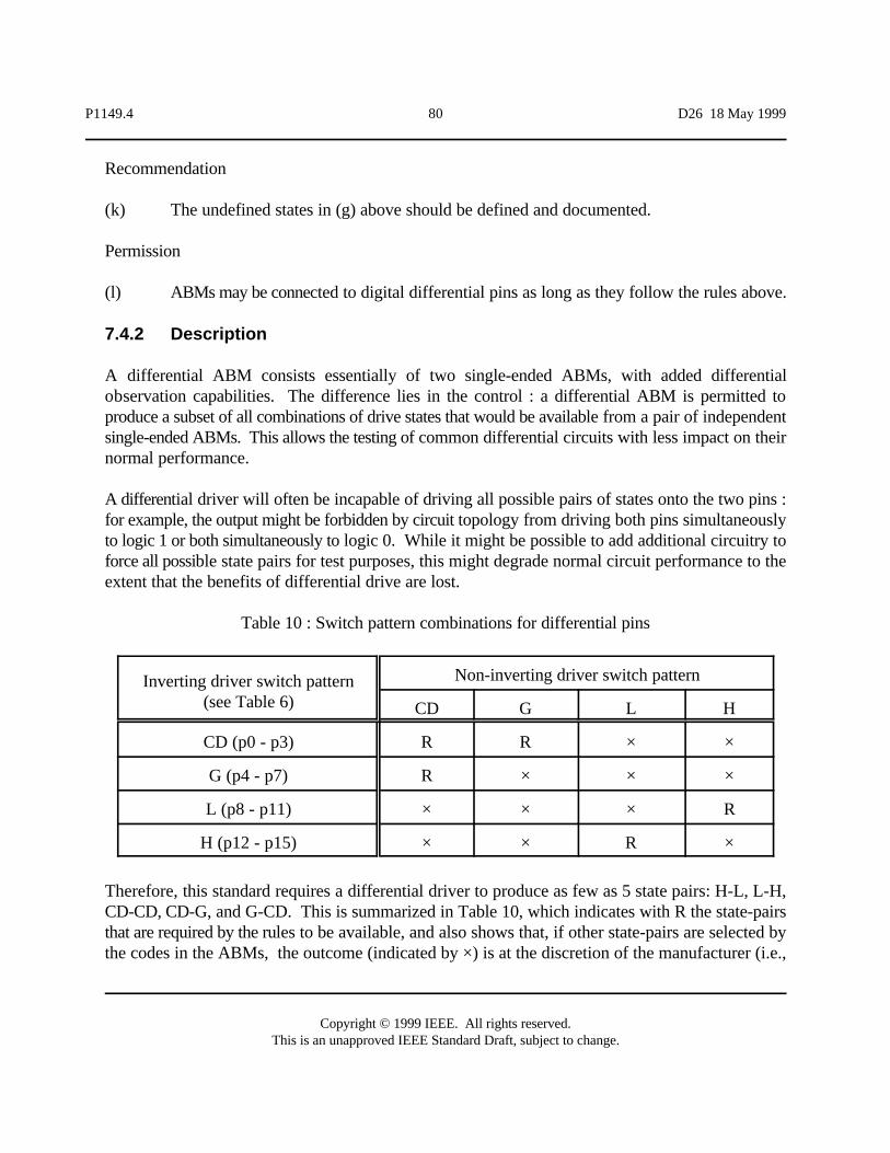
P1149.4 80 D26 18 May 1999
Copyright © 1999 IEEE. All rights reserved.This is an unapproved IEEE Standard Draft, subject to change.
Inverting driver switch pattern(see Table 6)
Non-inverting driver switch pattern
CD G L H
CD (p0 - p3) R R × ×
G (p4 - p7) R × × ×
L (p8 - p11) × × × R
H (p12 - p15) × × R ×
Table 10 : Switch pattern combinations for differential pins
Recommendation
(k) The undefined states in (g) above should be defined and documented.
Permission
(l) ABMs may be connected to digital differential pins as long as they follow the rules above.
7.4.2 Description
A differential ABM consists essentially of two single-ended ABMs, with added differentialobservation capabilities. The difference lies in the control : a differential ABM is permitted toproduce a subset of all combinations of drive states that would be available from a pair of independentsingle-ended ABMs. This allows the testing of common differential circuits with less impact on theirnormal performance.
A differential driver will often be incapable of driving all possible pairs of states onto the two pins :for example, the output might be forbidden by circuit topology from driving both pins simultaneouslyto logic 1 or both simultaneously to logic 0. While it might be possible to add additional circuitry toforce all possible state pairs for test purposes, this might degrade normal circuit performance to theextent that the benefits of differential drive are lost.
Therefore, this standard requires a differential driver to produce as few as 5 state pairs: H-L, L-H,CD-CD, CD-G, and G-CD. This is summarized in Table 10, which indicates with R the state-pairsthat are required by the rules to be available, and also shows that, if other state-pairs are selected bythe codes in the ABMs, the outcome (indicated by ×) is at the discretion of the manufacturer (i.e.,
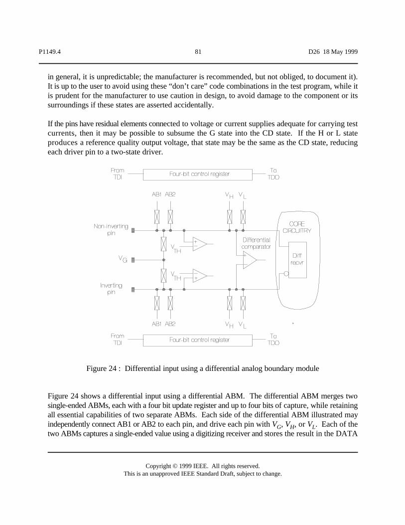
P1149.4 81 D26 18 May 1999
Copyright © 1999 IEEE. All rights reserved.This is an unapproved IEEE Standard Draft, subject to change.
Figure 24 : Differential input using a differential analog boundary module
in general, it is unpredictable; the manufacturer is recommended, but not obliged, to document it).It is up to the user to avoid using these “don’t care” code combinations in the test program, while itis prudent for the manufacturer to use caution in design, to avoid damage to the component or itssurroundings if these states are asserted accidentally.
If the pins have residual elements connected to voltage or current supplies adequate for carrying testcurrents, then it may be possible to subsume the G state into the CD state. If the H or L stateproduces a reference quality output voltage, that state may be the same as the CD state, reducingeach driver pin to a two-state driver.
Figure 24 shows a differential input using a differential ABM. The differential ABM merges twosingle-ended ABMs, each with a four bit update register and up to four bits of capture, while retainingall essential capabilities of two separate ABMs. Each side of the differential ABM illustrated mayindependently connect AB1 or AB2 to each pin, and drive each pin with V , V , or V . Each of theG H Ltwo ABMs captures a single-ended value using a digitizing receiver and stores the result in the DATA
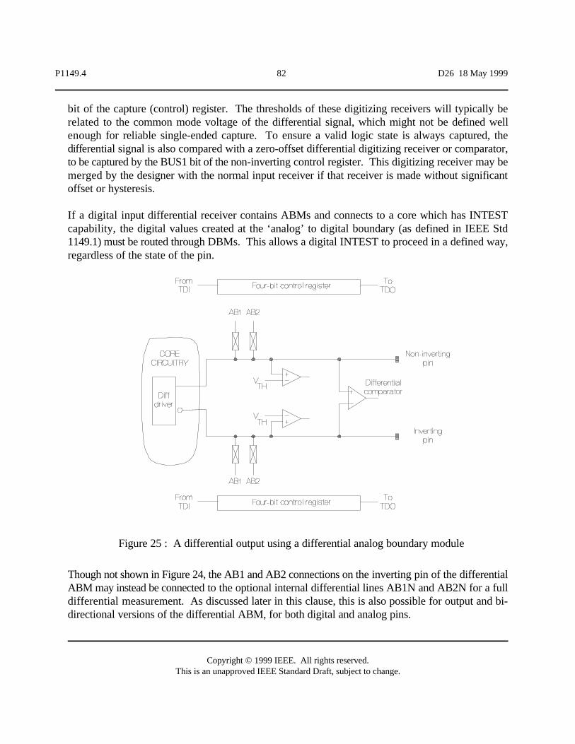
P1149.4 82 D26 18 May 1999
Copyright © 1999 IEEE. All rights reserved.This is an unapproved IEEE Standard Draft, subject to change.
Figure 25 : A differential output using a differential analog boundary module
bit of the capture (control) register. The thresholds of these digitizing receivers will typically berelated to the common mode voltage of the differential signal, which might not be defined wellenough for reliable single-ended capture. To ensure a valid logic state is always captured, thedifferential signal is also compared with a zero-offset differential digitizing receiver or comparator,to be captured by the BUS1 bit of the non-inverting control register. This digitizing receiver may bemerged by the designer with the normal input receiver if that receiver is made without significantoffset or hysteresis.
If a digital input differential receiver contains ABMs and connects to a core which has INTESTcapability, the digital values created at the ‘analog’ to digital boundary (as defined in IEEE Std1149.1) must be routed through DBMs. This allows a digital INTEST to proceed in a defined way,regardless of the state of the pin.
Though not shown in Figure 24, the AB1 and AB2 connections on the inverting pin of the differentialABM may instead be connected to the optional internal differential lines AB1N and AB2N for a fulldifferential measurement. As discussed later in this clause, this is also possible for output and bi-directional versions of the differential ABM, for both digital and analog pins.
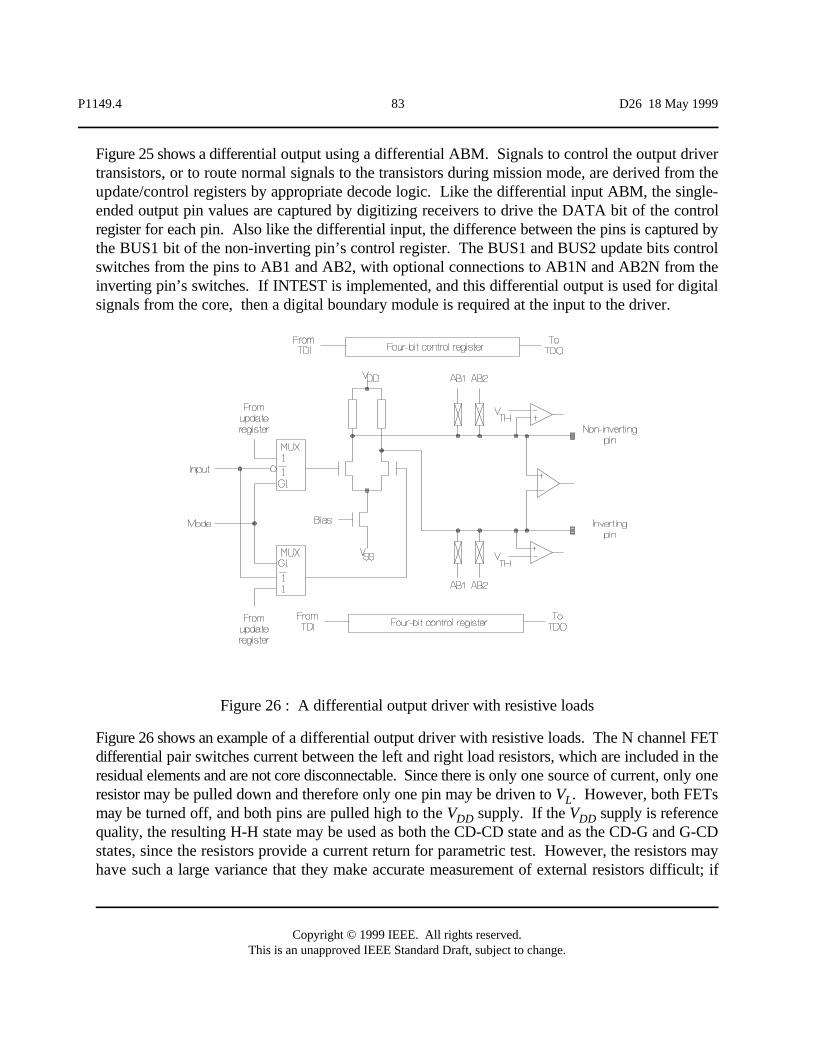
P1149.4 83 D26 18 May 1999
Copyright © 1999 IEEE. All rights reserved.This is an unapproved IEEE Standard Draft, subject to change.
Figure 26 : A differential output driver with resistive loads
Figure 25 shows a differential output using a differential ABM. Signals to control the output drivertransistors, or to route normal signals to the transistors during mission mode, are derived from theupdate/control registers by appropriate decode logic. Like the differential input ABM, the single-ended output pin values are captured by digitizing receivers to drive the DATA bit of the controlregister for each pin. Also like the differential input, the difference between the pins is captured bythe BUS1 bit of the non-inverting pin’s control register. The BUS1 and BUS2 update bits controlswitches from the pins to AB1 and AB2, with optional connections to AB1N and AB2N from theinverting pin’s switches. If INTEST is implemented, and this differential output is used for digitalsignals from the core, then a digital boundary module is required at the input to the driver.
Figure 26 shows an example of a differential output driver with resistive loads. The N channel FETdifferential pair switches current between the left and right load resistors, which are included in theresidual elements and are not core disconnectable. Since there is only one source of current, only oneresistor may be pulled down and therefore only one pin may be driven to V . However, both FETsLmay be turned off, and both pins are pulled high to the V supply. If the V supply is referenceDD DDquality, the resulting H-H state may be used as both the CD-CD state and as the CD-G and G-CDstates, since the resistors provide a current return for parametric test. However, the resistors mayhave such a large variance that they make accurate measurement of external resistors difficult; if
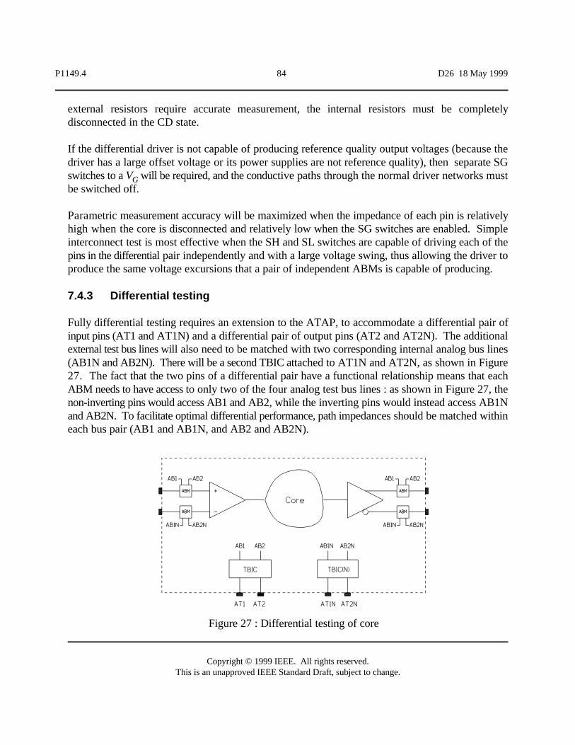
P1149.4 84 D26 18 May 1999
Copyright © 1999 IEEE. All rights reserved.This is an unapproved IEEE Standard Draft, subject to change.
Figure 27 : Differential testing of core
external resistors require accurate measurement, the internal resistors must be completelydisconnected in the CD state.
If the differential driver is not capable of producing reference quality output voltages (because thedriver has a large offset voltage or its power supplies are not reference quality), then separate SGswitches to a V will be required, and the conductive paths through the normal driver networks mustGbe switched off.
Parametric measurement accuracy will be maximized when the impedance of each pin is relativelyhigh when the core is disconnected and relatively low when the SG switches are enabled. Simpleinterconnect test is most effective when the SH and SL switches are capable of driving each of thepins in the differential pair independently and with a large voltage swing, thus allowing the driver toproduce the same voltage excursions that a pair of independent ABMs is capable of producing.
7.4.3 Differential testing
Fully differential testing requires an extension to the ATAP, to accommodate a differential pair ofinput pins (AT1 and AT1N) and a differential pair of output pins (AT2 and AT2N). The additionalexternal test bus lines will also need to be matched with two corresponding internal analog bus lines(AB1N and AB2N). There will be a second TBIC attached to AT1N and AT2N, as shown in Figure27. The fact that the two pins of a differential pair have a functional relationship means that eachABM needs to have access to only two of the four analog test bus lines : as shown in Figure 27, thenon-inverting pins would access AB1 and AB2, while the inverting pins would instead access AB1Nand AB2N. To facilitate optimal differential performance, path impedances should be matched withineach bus pair (AB1 and AB1N, and AB2 and AB2N).
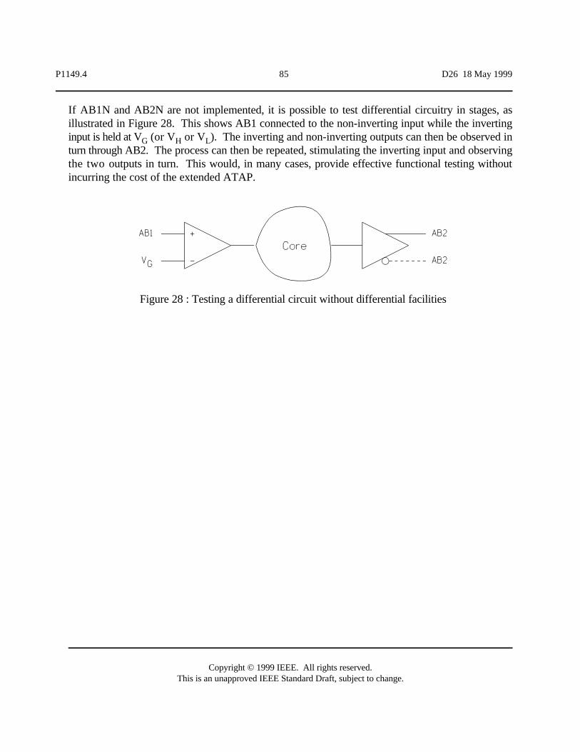
P1149.4 85 D26 18 May 1999
Copyright © 1999 IEEE. All rights reserved.This is an unapproved IEEE Standard Draft, subject to change.
Figure 28 : Testing a differential circuit without differential facilities
If AB1N and AB2N are not implemented, it is possible to test differential circuitry in stages, asillustrated in Figure 28. This shows AB1 connected to the non-inverting input while the invertinginput is held at V (or V or V ). The inverting and non-inverting outputs can then be observed inG H Lturn through AB2. The process can then be repeated, stimulating the inverting input and observingthe two outputs in turn. This would, in many cases, provide effective functional testing withoutincurring the cost of the extended ATAP.
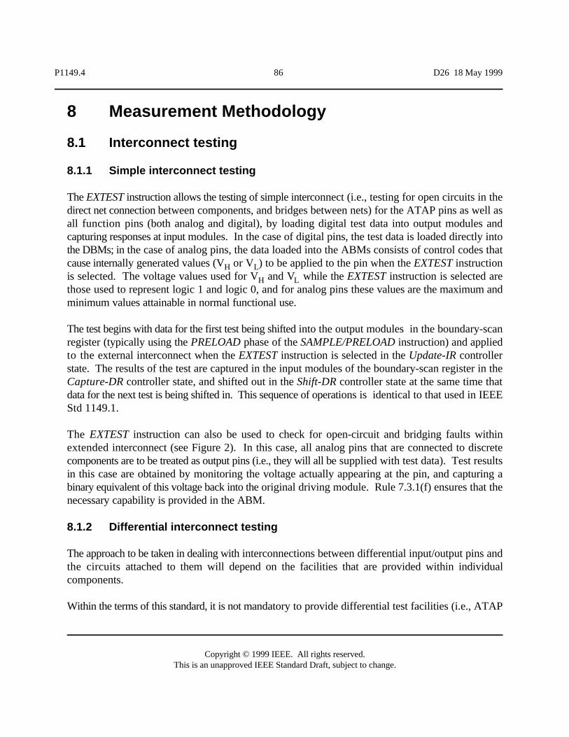
P1149.4 86 D26 18 May 1999
Copyright © 1999 IEEE. All rights reserved.This is an unapproved IEEE Standard Draft, subject to change.
8 Measurement Methodology
8.1 Interconnect testing
8.1.1 Simple interconnect testing
The EXTEST instruction allows the testing of simple interconnect (i.e., testing for open circuits in thedirect net connection between components, and bridges between nets) for the ATAP pins as well asall function pins (both analog and digital), by loading digital test data into output modules andcapturing responses at input modules. In the case of digital pins, the test data is loaded directly intothe DBMs; in the case of analog pins, the data loaded into the ABMs consists of control codes thatcause internally generated values (V or V ) to be applied to the pin when the EXTEST instructionH Lis selected. The voltage values used for V and V while the EXTEST instruction is selected areH Lthose used to represent logic 1 and logic 0, and for analog pins these values are the maximum andminimum values attainable in normal functional use.
The test begins with data for the first test being shifted into the output modules in the boundary-scanregister (typically using the PRELOAD phase of the SAMPLE/PRELOAD instruction) and appliedto the external interconnect when the EXTEST instruction is selected in the Update-IR controllerstate. The results of the test are captured in the input modules of the boundary-scan register in theCapture-DR controller state, and shifted out in the Shift-DR controller state at the same time thatdata for the next test is being shifted in. This sequence of operations is identical to that used in IEEEStd 1149.1.
The EXTEST instruction can also be used to check for open-circuit and bridging faults withinextended interconnect (see Figure 2). In this case, all analog pins that are connected to discretecomponents are to be treated as output pins (i.e., they will all be supplied with test data). Test resultsin this case are obtained by monitoring the voltage actually appearing at the pin, and capturing abinary equivalent of this voltage back into the original driving module. Rule 7.3.1(f) ensures that thenecessary capability is provided in the ABM.
8.1.2 Differential interconnect testing
The approach to be taken in dealing with interconnections between differential input/output pins andthe circuits attached to them will depend on the facilities that are provided within individualcomponents.
Within the terms of this standard, it is not mandatory to provide differential test facilities (i.e., ATAP
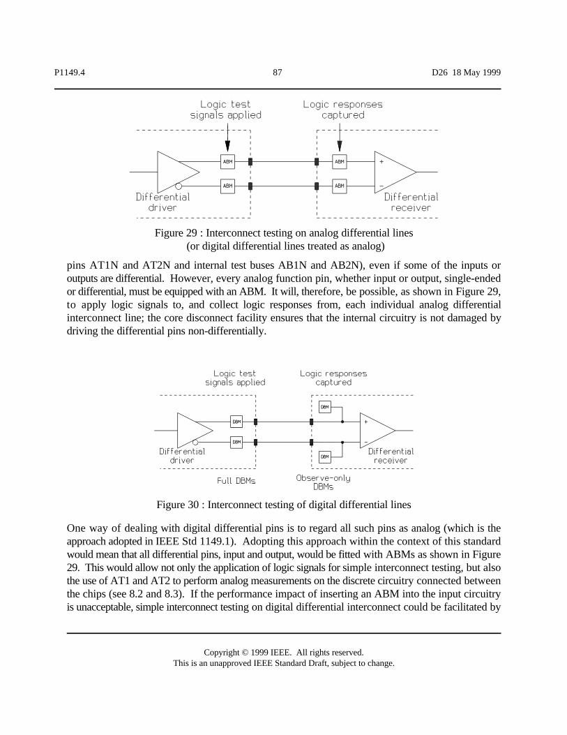
P1149.4 87 D26 18 May 1999
Copyright © 1999 IEEE. All rights reserved.This is an unapproved IEEE Standard Draft, subject to change.
Figure 29 : Interconnect testing on analog differential lines (or digital differential lines treated as analog)
Figure 30 : Interconnect testing of digital differential lines
pins AT1N and AT2N and internal test buses AB1N and AB2N), even if some of the inputs oroutputs are differential. However, every analog function pin, whether input or output, single-endedor differential, must be equipped with an ABM. It will, therefore, be possible, as shown in Figure 29,to apply logic signals to, and collect logic responses from, each individual analog differentialinterconnect line; the core disconnect facility ensures that the internal circuitry is not damaged bydriving the differential pins non-differentially.
One way of dealing with digital differential pins is to regard all such pins as analog (which is theapproach adopted in IEEE Std 1149.1). Adopting this approach within the context of this standardwould mean that all differential pins, input and output, would be fitted with ABMs as shown in Figure29. This would allow not only the application of logic signals for simple interconnect testing, but alsothe use of AT1 and AT2 to perform analog measurements on the discrete circuitry connected betweenthe chips (see 8.2 and 8.3). If the performance impact of inserting an ABM into the input circuitryis unacceptable, simple interconnect testing on digital differential interconnect could be facilitated by
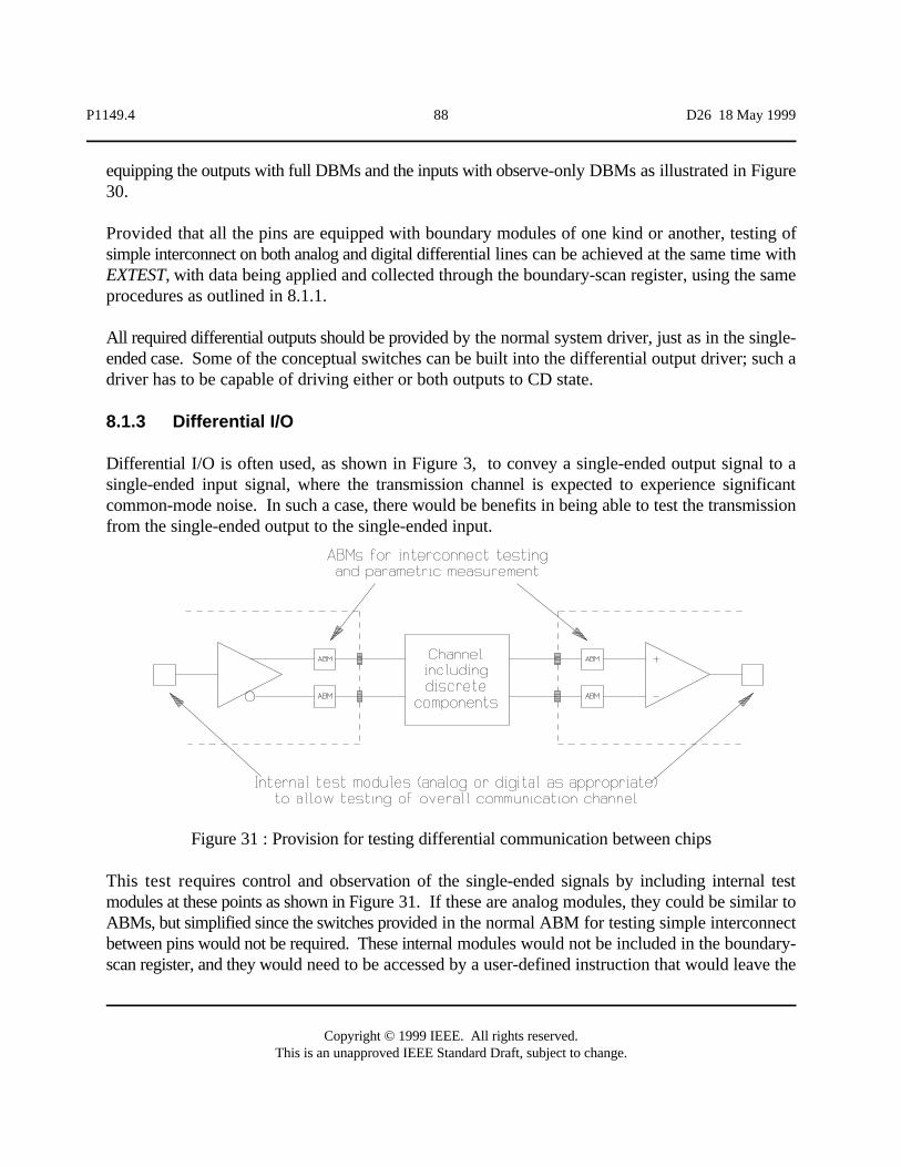
P1149.4 88 D26 18 May 1999
Copyright © 1999 IEEE. All rights reserved.This is an unapproved IEEE Standard Draft, subject to change.
Figure 31 : Provision for testing differential communication between chips
equipping the outputs with full DBMs and the inputs with observe-only DBMs as illustrated in Figure30.
Provided that all the pins are equipped with boundary modules of one kind or another, testing ofsimple interconnect on both analog and digital differential lines can be achieved at the same time withEXTEST, with data being applied and collected through the boundary-scan register, using the sameprocedures as outlined in 8.1.1.
All required differential outputs should be provided by the normal system driver, just as in the single-ended case. Some of the conceptual switches can be built into the differential output driver; such adriver has to be capable of driving either or both outputs to CD state.
8.1.3 Differential I/O
Differential I/O is often used, as shown in Figure 3, to convey a single-ended output signal to asingle-ended input signal, where the transmission channel is expected to experience significantcommon-mode noise. In such a case, there would be benefits in being able to test the transmissionfrom the single-ended output to the single-ended input.
This test requires control and observation of the single-ended signals by including internal testmodules at these points as shown in Figure 31. If these are analog modules, they could be similar toABMs, but simplified since the switches provided in the normal ABM for testing simple interconnectbetween pins would not be required. These internal modules would not be included in the boundary-scan register, and they would need to be accessed by a user-defined instruction that would leave the
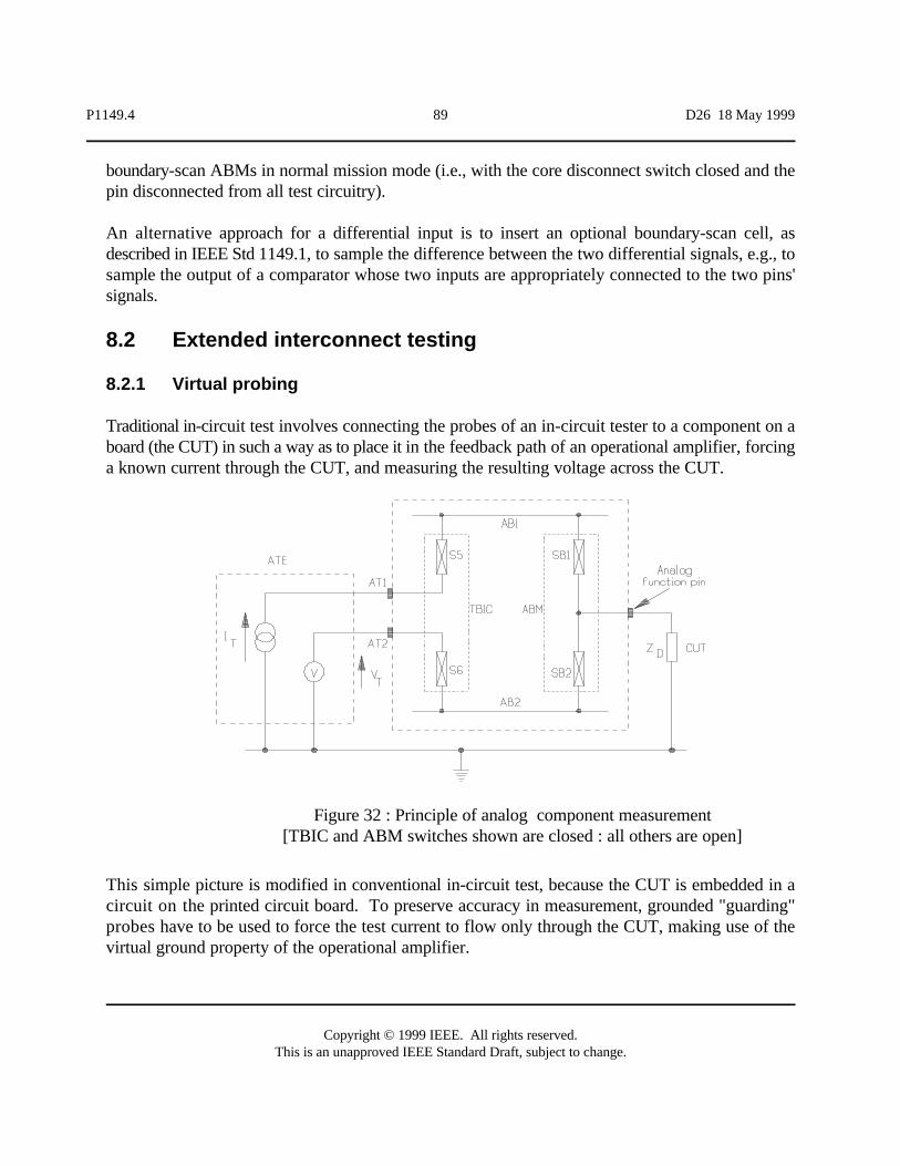
P1149.4 89 D26 18 May 1999
Copyright © 1999 IEEE. All rights reserved.This is an unapproved IEEE Standard Draft, subject to change.
Figure 32 : Principle of analog component measurement[TBIC and ABM switches shown are closed : all others are open]
boundary-scan ABMs in normal mission mode (i.e., with the core disconnect switch closed and thepin disconnected from all test circuitry).
An alternative approach for a differential input is to insert an optional boundary-scan cell, asdescribed in IEEE Std 1149.1, to sample the difference between the two differential signals, e.g., tosample the output of a comparator whose two inputs are appropriately connected to the two pins'signals.
8.2 Extended interconnect testing
8.2.1 Virtual probing
Traditional in-circuit test involves connecting the probes of an in-circuit tester to a component on aboard (the CUT) in such a way as to place it in the feedback path of an operational amplifier, forcinga known current through the CUT, and measuring the resulting voltage across the CUT.
This simple picture is modified in conventional in-circuit test, because the CUT is embedded in acircuit on the printed circuit board. To preserve accuracy in measurement, grounded "guarding"probes have to be used to force the test current to flow only through the CUT, making use of thevirtual ground property of the operational amplifier.
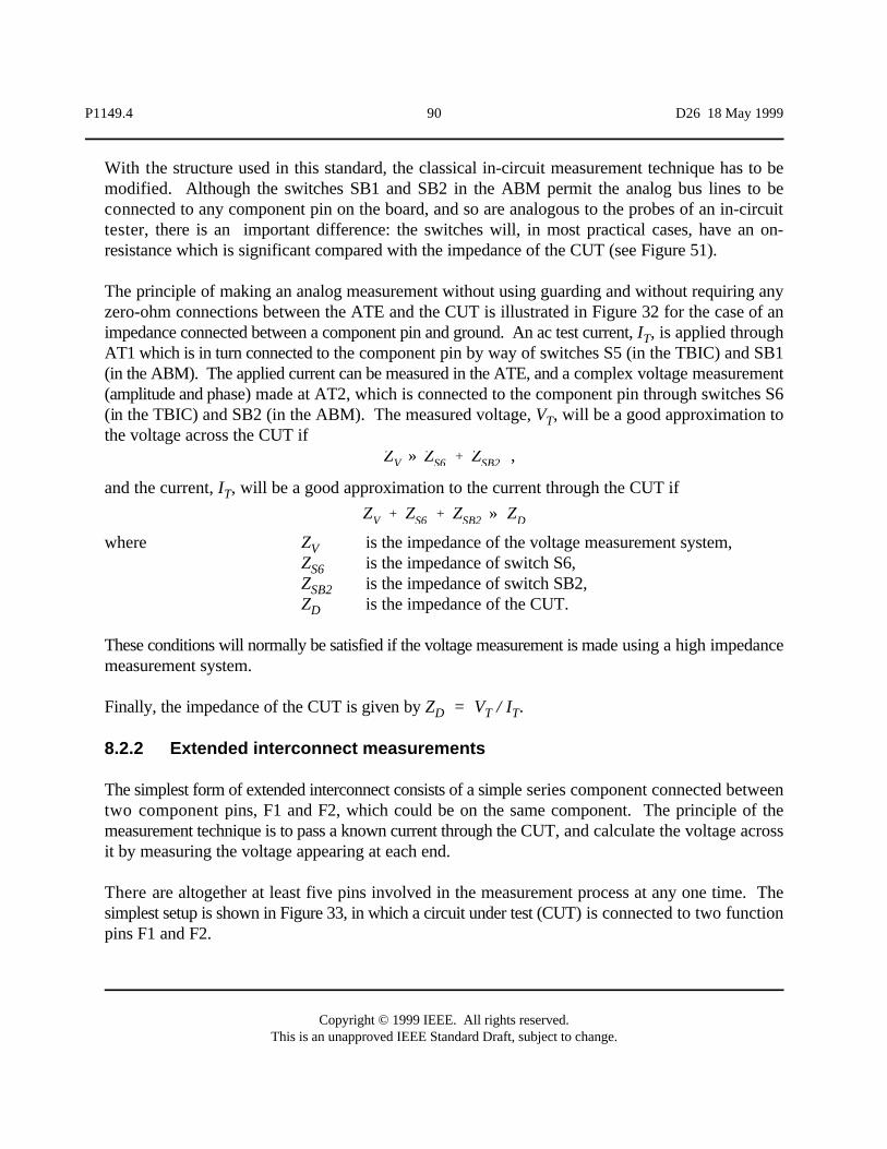
ZV » ZS6 % ZSB2
ZV % ZS6 % ZSB2 » ZD
P1149.4 90 D26 18 May 1999
Copyright © 1999 IEEE. All rights reserved.This is an unapproved IEEE Standard Draft, subject to change.
With the structure used in this standard, the classical in-circuit measurement technique has to bemodified. Although the switches SB1 and SB2 in the ABM permit the analog bus lines to beconnected to any component pin on the board, and so are analogous to the probes of an in-circuittester, there is an important difference: the switches will, in most practical cases, have an on-resistance which is significant compared with the impedance of the CUT (see Figure 51).
The principle of making an analog measurement without using guarding and without requiring anyzero-ohm connections between the ATE and the CUT is illustrated in Figure 32 for the case of animpedance connected between a component pin and ground. An ac test current, I , is applied throughTAT1 which is in turn connected to the component pin by way of switches S5 (in the TBIC) and SB1(in the ABM). The applied current can be measured in the ATE, and a complex voltage measurement(amplitude and phase) made at AT2, which is connected to the component pin through switches S6(in the TBIC) and SB2 (in the ABM). The measured voltage, V , will be a good approximation toTthe voltage across the CUT if
,
and the current, I , will be a good approximation to the current through the CUT ifT
where Z is the impedance of the voltage measurement system,VZ is the impedance of switch S6,S6Z is the impedance of switch SB2,SB2Z is the impedance of the CUT.D
These conditions will normally be satisfied if the voltage measurement is made using a high impedancemeasurement system.
Finally, the impedance of the CUT is given by Z = V / I .D T T
8.2.2 Extended interconnect measurements
The simplest form of extended interconnect consists of a simple series component connected betweentwo component pins, F1 and F2, which could be on the same component. The principle of themeasurement technique is to pass a known current through the CUT, and calculate the voltage acrossit by measuring the voltage appearing at each end.
There are altogether at least five pins involved in the measurement process at any one time. Thesimplest setup is shown in Figure 33, in which a circuit under test (CUT) is connected to two functionpins F1 and F2.
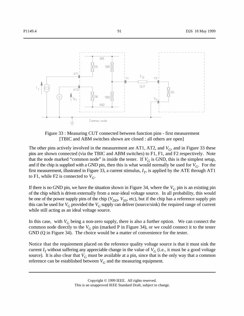
P1149.4 91 D26 18 May 1999
Copyright © 1999 IEEE. All rights reserved.This is an unapproved IEEE Standard Draft, subject to change.
Figure 33 : Measuring CUT connected between function pins - first measurement[TBIC and ABM switches shown are closed : all others are open]
The other pins actively involved in the measurement are AT1, AT2, and V , and in Figure 33 theseGpins are shown connected (via the TBIC and ABM switches) to F1, F1, and F2 respectively. Notethat the node marked “common node” is inside the tester. If V is GND, this is the simplest setup,Gand if the chip is supplied with a GND pin, then this is what would normally be used for V . For theGfirst measurement, illustrated in Figure 33, a current stimulus, I , is applied by the ATE through AT1Tto F1, while F2 is connected to V .G
If there is no GND pin, we have the situation shown in Figure 34, where the V pin is an existing pinGof the chip which is driven externally from a near-ideal voltage source. In all probability, this wouldbe one of the power supply pins of the chip (V , V , etc), but if the chip has a reference supply pinDD SSthis can be used for V provided the V supply can deliver (source/sink) the required range of currentG Gwhile still acting as an ideal voltage source.
In this case, with V being a non-zero supply, there is also a further option. We can connect theGcommon node directly to the V pin (marked P in Figure 34), or we could connect it to the testerGGND (Q in Figure 34). The choice would be a matter of convenience for the tester.
Notice that the requirement placed on the reference quality voltage source is that it must sink thecurrent I without suffering any appreciable change in the value of V (i.e., it must be a good voltageT Gsource). It is also clear that V must be available at a pin, since that is the only way that a commonGreference can be established between V and the measuring equipment.G
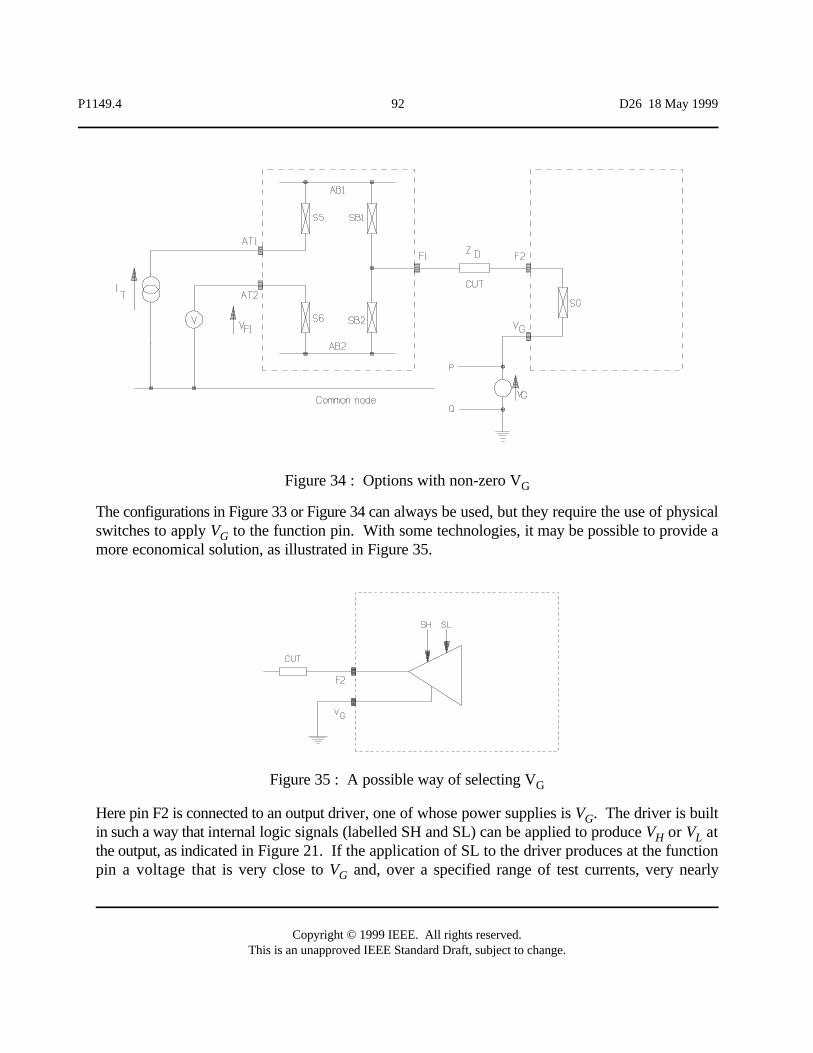
P1149.4 92 D26 18 May 1999
Copyright © 1999 IEEE. All rights reserved.This is an unapproved IEEE Standard Draft, subject to change.
Figure 34 : Options with non-zero VG
Figure 35 : A possible way of selecting VG
The configurations in Figure 33 or Figure 34 can always be used, but they require the use of physicalswitches to apply V to the function pin. With some technologies, it may be possible to provide aGmore economical solution, as illustrated in Figure 35.
Here pin F2 is connected to an output driver, one of whose power supplies is V . The driver is builtGin such a way that internal logic signals (labelled SH and SL) can be applied to produce V or V atH Lthe output, as indicated in Figure 21. If the application of SL to the driver produces at the functionpin a voltage that is very close to V and, over a specified range of test currents, very nearlyG
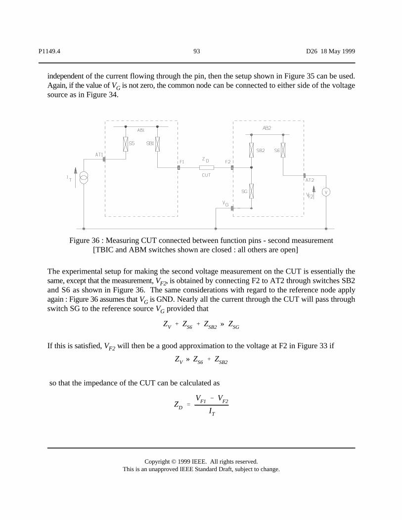
ZV % ZS6 % ZSB2 » ZSG
ZV » ZS6 % ZSB2
ZD 'VF1 & VF2
IT
P1149.4 93 D26 18 May 1999
Copyright © 1999 IEEE. All rights reserved.This is an unapproved IEEE Standard Draft, subject to change.
Figure 36 : Measuring CUT connected between function pins - second measurement[TBIC and ABM switches shown are closed : all others are open]
independent of the current flowing through the pin, then the setup shown in Figure 35 can be used.Again, if the value of V is not zero, the common node can be connected to either side of the voltageGsource as in Figure 34.
The experimental setup for making the second voltage measurement on the CUT is essentially thesame, except that the measurement, V , is obtained by connecting F2 to AT2 through switches SB2F2and S6 as shown in Figure 36. The same considerations with regard to the reference node applyagain : Figure 36 assumes that V is GND. Nearly all the current through the CUT will pass throughGswitch SG to the reference source V provided that G
If this is satisfied, V will then be a good approximation to the voltage at F2 in Figure 33 if F2
so that the impedance of the CUT can be calculated as
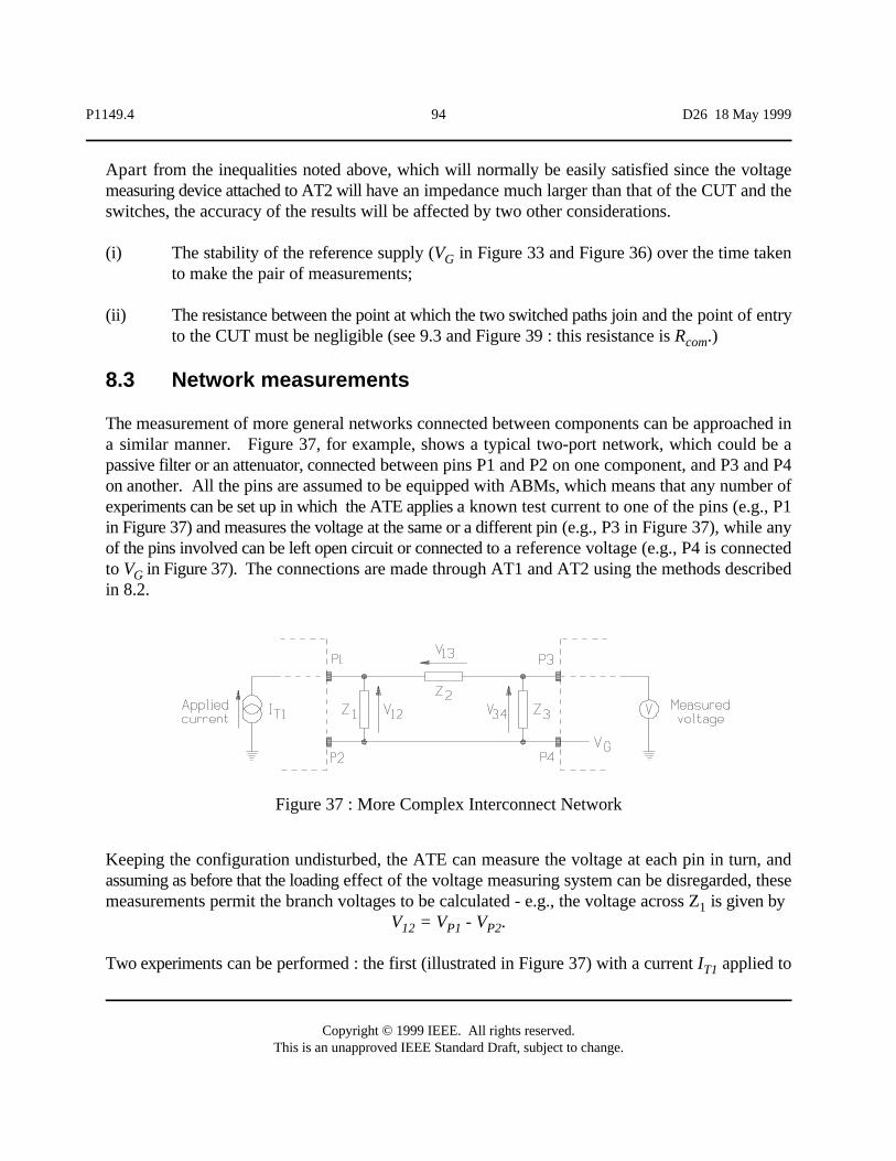
P1149.4 94 D26 18 May 1999
Copyright © 1999 IEEE. All rights reserved.This is an unapproved IEEE Standard Draft, subject to change.
Figure 37 : More Complex Interconnect Network
Apart from the inequalities noted above, which will normally be easily satisfied since the voltagemeasuring device attached to AT2 will have an impedance much larger than that of the CUT and theswitches, the accuracy of the results will be affected by two other considerations.
(i) The stability of the reference supply (V in Figure 33 and Figure 36) over the time takenGto make the pair of measurements;
(ii) The resistance between the point at which the two switched paths join and the point of entryto the CUT must be negligible (see 9.3 and Figure 39 : this resistance is R .)com
8.3 Network measurements
The measurement of more general networks connected between components can be approached ina similar manner. Figure 37, for example, shows a typical two-port network, which could be apassive filter or an attenuator, connected between pins P1 and P2 on one component, and P3 and P4on another. All the pins are assumed to be equipped with ABMs, which means that any number ofexperiments can be set up in which the ATE applies a known test current to one of the pins (e.g., P1in Figure 37) and measures the voltage at the same or a different pin (e.g., P3 in Figure 37), while anyof the pins involved can be left open circuit or connected to a reference voltage (e.g., P4 is connectedto V in Figure 37). The connections are made through AT1 and AT2 using the methods describedGin 8.2.
Keeping the configuration undisturbed, the ATE can measure the voltage at each pin in turn, andassuming as before that the loading effect of the voltage measuring system can be disregarded, thesemeasurements permit the branch voltages to be calculated - e.g., the voltage across Z is given by 1
V = V - V .12 P1 P2
Two experiments can be performed : the first (illustrated in Figure 37) with a current I applied toT1
P1149.4 95 D26 18 May 1999
Copyright © 1999 IEEE. All rights reserved.This is an unapproved IEEE Standard Draft, subject to change.
P1 with P3 open circuit and P2 (or P4) connected to a reference (V ); and the second with currentGI (where I could be, but is not necessarily, the same as I ) applied to P3 with P1 open circuit.T2 T2 T1
With this particular network, there are five unknowns : the three impedances Z , Z , and Z the1 2 3,applied reference voltage, V , and the switch impedance associated with V . With three voltageG Gmeasurements obtained from each of the two experiments, we therefore have enough data with whichto calculate the three branch impedances of interest. For more complicated networks, where thenumber of elements exceeds the number of measurements that are available, a special metrology hasbeen developed using simulation to supply additional data. This metrology is fully described in thepaper by Parker et al (see 1.4).
P1149.4 96 D26 18 May 1999
Copyright © 1999 IEEE. All rights reserved.This is an unapproved IEEE Standard Draft, subject to change.
9 Analog parametric limits
9.1 General
An objective of this standard is to facilitate measurement of complex impedances with an accuracybetter than ±1% when measuring impedances between 10 S and 100 kS, with a 1 kHz bandwidthanywhere between 100 Hz and 10 kHz. Many systematic sources of error can be characterized andhence may not contribute to this error. Other sources cannot be measured and must be minimized.The ability to achieve this level of accuracy ultimately depends upon the analog characteristics of thebuses, the switches, the CUT, and the ATE. These in turn depend on the way the standard isimplemented, and also on details of the layout and design. This clause defines performance limits thatneed to be met if the required accuracy is to be achieved, based on measurements that can be madeusing the test bus structure itself.
Factors that affect performance include the way in which the switches in the TBIC and the ABMs areimplemented, and also the measures taken to provide electrostatic protection to the chip. The rulesthat follow try to anticipate a large variety of power supply voltages, switch implementations, and busarchitectures, while assuming use of state-of-the-art measurement equipment and techniques.
The standard provides facilities for calibration, which allows some potential errors to be cancelled orcompensated, but there will be other errors due to inevitable practical limitations; these will have tobe minimized by careful design.
In the remainder of this clause, the most positive and negative pin-specific power supply voltages aredenoted by V and V respectively. Some voltages and resistances are only measurable in certainDD SSABM and/or TBIC states, and may not correspond to a specific pin or element. For example, V isHthe unloaded voltage present at a function pin, and might be equal to the voltage (V ) at the VDD DDpin minus some offset voltage; R is the resistance across two switches (S6 and SB1) and issw1measurable only as the sum of the switch resistances, R + R .S6 SB1
9.2 Switch limitations
The key architectural features of this standard are the TBIC and the ABM, both of which are definedas consisting largely of conceptual switches. When the standard is implemented, these conceptualswitches can be realized in a number of ways. It might be convenient, for example, particularly inCMOS circuits, to use transmission gates; in some cases the necessary switching functions can beintegrated with system drivers or receivers; and any or all of the switches may be implemented using3-state voltage buffers and/or current buffers, as shown in Figure 38.
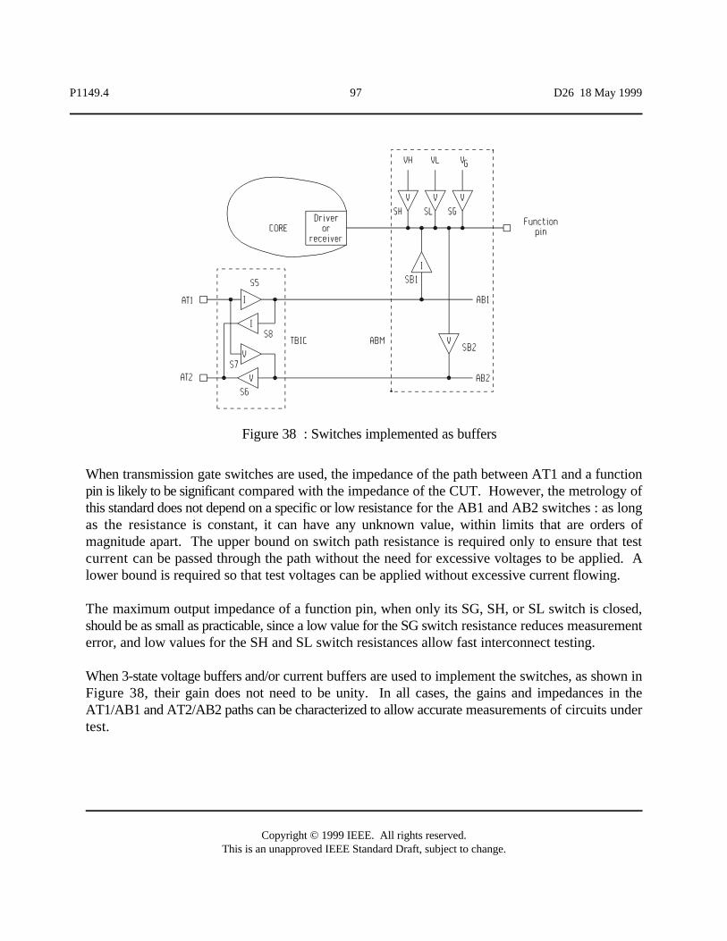
P1149.4 97 D26 18 May 1999
Copyright © 1999 IEEE. All rights reserved.This is an unapproved IEEE Standard Draft, subject to change.
Figure 38 : Switches implemented as buffers
When transmission gate switches are used, the impedance of the path between AT1 and a functionpin is likely to be significant compared with the impedance of the CUT. However, the metrology ofthis standard does not depend on a specific or low resistance for the AB1 and AB2 switches : as longas the resistance is constant, it can have any unknown value, within limits that are orders ofmagnitude apart. The upper bound on switch path resistance is required only to ensure that testcurrent can be passed through the path without the need for excessive voltages to be applied. Alower bound is required so that test voltages can be applied without excessive current flowing.
The maximum output impedance of a function pin, when only its SG, SH, or SL switch is closed,should be as small as practicable, since a low value for the SG switch resistance reduces measurementerror, and low values for the SH and SL switch resistances allow fast interconnect testing.
When 3-state voltage buffers and/or current buffers are used to implement the switches, as shown inFigure 38, their gain does not need to be unity. In all cases, the gains and impedances in theAT1/AB1 and AT2/AB2 paths can be characterized to allow accurate measurements of circuits undertest.
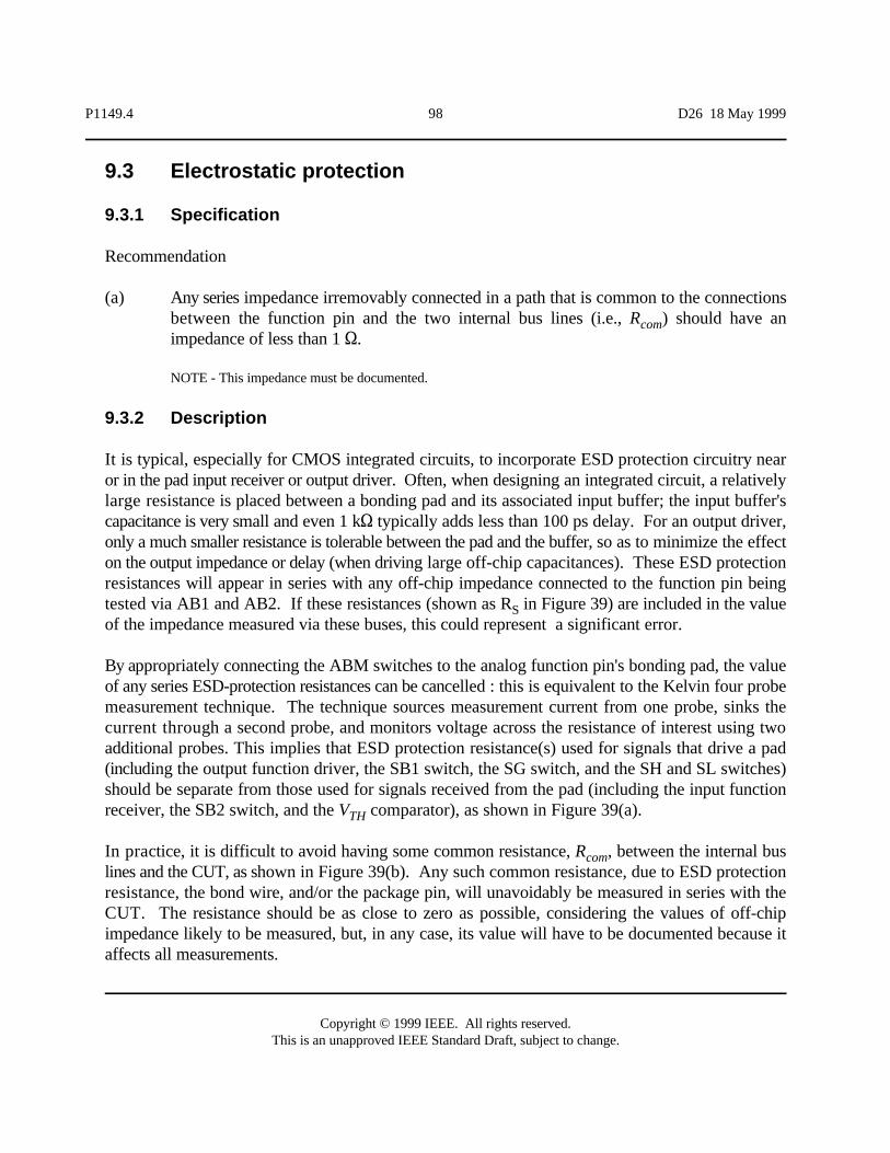
P1149.4 98 D26 18 May 1999
Copyright © 1999 IEEE. All rights reserved.This is an unapproved IEEE Standard Draft, subject to change.
9.3 Electrostatic protection
9.3.1 Specification
Recommendation
(a) Any series impedance irremovably connected in a path that is common to the connectionsbetween the function pin and the two internal bus lines (i.e., R ) should have ancomimpedance of less than 1 S.
NOTE - This impedance must be documented.
9.3.2 Description
It is typical, especially for CMOS integrated circuits, to incorporate ESD protection circuitry nearor in the pad input receiver or output driver. Often, when designing an integrated circuit, a relativelylarge resistance is placed between a bonding pad and its associated input buffer; the input buffer'scapacitance is very small and even 1 kS typically adds less than 100 ps delay. For an output driver,only a much smaller resistance is tolerable between the pad and the buffer, so as to minimize the effecton the output impedance or delay (when driving large off-chip capacitances). These ESD protectionresistances will appear in series with any off-chip impedance connected to the function pin beingtested via AB1 and AB2. If these resistances (shown as R in Figure 39) are included in the valueSof the impedance measured via these buses, this could represent a significant error.
By appropriately connecting the ABM switches to the analog function pin's bonding pad, the valueof any series ESD-protection resistances can be cancelled : this is equivalent to the Kelvin four probemeasurement technique. The technique sources measurement current from one probe, sinks thecurrent through a second probe, and monitors voltage across the resistance of interest using twoadditional probes. This implies that ESD protection resistance(s) used for signals that drive a pad(including the output function driver, the SB1 switch, the SG switch, and the SH and SL switches)should be separate from those used for signals received from the pad (including the input functionreceiver, the SB2 switch, and the V comparator), as shown in Figure 39(a).TH
In practice, it is difficult to avoid having some common resistance, R , between the internal buscomlines and the CUT, as shown in Figure 39(b). Any such common resistance, due to ESD protectionresistance, the bond wire, and/or the package pin, will unavoidably be measured in series with theCUT. The resistance should be as close to zero as possible, considering the values of off-chipimpedance likely to be measured, but, in any case, its value will have to be documented because itaffects all measurements.
VDD&VSS&200 mV
200 µA
P1149.4 99 D26 18 May 1999
Copyright © 1999 IEEE. All rights reserved.This is an unapproved IEEE Standard Draft, subject to change.
Figure 39 : Switch connections to bonding pad/pin
9.4 Performance specifications
Rules
(a) When transmission gate switches are used, R , the maximum incremental switchsw1resistance in the AT1 path (measured between AT1 and each function pin while thefunction pin is driven to any dc voltage between V and V ), shall beDD SS
or 10 kS , whichever is less.
NOTE -This will include the TBIC AT1-AB1 switch ( S5 in Figure 12 and Figure 42).
(b) When transmission gate switches are used, R , the maximum incremental switch resistancesw2in the AT2 path (measured between AT2 and each function pin while the function pin isdriven to any dc voltage between V and V ), shall be 10 kS. DD SS
NOTE - This will include the TBIC AB2-AT2 switch (S6 in Figure 12 and Figure 43).
(c) When the function output driver for an output pin is not used for driving V and V , theH L

VDD&VSS&200 mV
200 µA
P1149.4 100 D26 18 May 1999
Copyright © 1999 IEEE. All rights reserved.This is an unapproved IEEE Standard Draft, subject to change.
maximum output resistance for V and V , measured between the function pin and V orH L DDV respectively shall be 10 kS.SS
NOTE - This will include the ABM switch between the function pin and V or V (SH or SL in Figure 19).H L
(d) The maximum output resistance for V , measured between each function pin and the pinGused to supply (see10.2.1), using a 100 µA amplitude, 1 kHz sine wave stimulus current,
shall be or 10 kS , whichever is less.
(e) When a current buffer is used as a switch in the AT1 to AB1 path, or in the AB1 to functionpin path,
(i) it shall be capable of delivering a 1kHz sine wave stimulus of 100 µA peakamplitude at the function pin;
(ii) the absolute value of the current gain shall be between 0.5 and 2;
(iii) input currents that exceed the capability of the buffer shall cause the buffer tosaturate.
NOTE - Since the current gain is not necessarily unity, the current range at AT1 may be less than ±100 µA.
(f) When a voltage buffer is used as a switch in the function pin to AB2 path, or in the AB2 toAT2 path,
(i) it shall be capable of monitoring a 1 kHz sine wave stimulus of 100 mV peakamplitude with a bias of any voltage between V and V at the function pin;DD SS
(ii) the maximum absolute value of the voltage gain shall be unity;
(iii) input voltages that exceed the capability of the buffer shall cause the buffer tosaturate.
NOTE - Because the voltage gain may be less than unity, the voltage range at AT2 may be less than its V -V .DD SS
(g) When delivering, via AT1, a 1 kHz sinusoidal current of 100 µA amplitude to a 1 kSresistor connected to a function pin, and measuring the voltage via AT2 using a voltmeter
P1149.4 101 D26 18 May 1999
Copyright © 1999 IEEE. All rights reserved.This is an unapproved IEEE Standard Draft, subject to change.
with a -3 dB bandwidth greater than 1 kHz, the measurement error shall be less than 1%.This shall be true when the resistor is connected to any voltage between V and V , forSS DDall operating conditions, while applying pattern P3 (see 7.3.2) to the pin and pattern P0 toall other function pins. Parasitic impedance values that are documented (see 10.2) or thatcan be measured via AT1 and AT2 without involving any function pins may be used toadjust the measured value before calculating the measurement error. (See 9.6.)
(h) When delivering a 1 kHz sinusoidal current of 100 µA amplitude to a function pin, andmeasuring the voltage via AT2, using a voltmeter with a -3 dB bandwidth greater than1 kHz, the measured voltage shall vary by no more than 1 mV over a time interval of 1 sec.
(i) When an ATAP pin is not specified elsewhere in this standard to be connected to V , V ,H LV , AB1, AB1N, AB2, or AB2N, the resistance measured between the ATAP pin and theGV pin, for any applied voltage between V and V shall be greater than 2 MS, and theG DD SScapacitance shall be less than 10 pF.
(j) When an ATAP pin is not specified elsewhere in this standard to be connected to V , V ,H LV , AB1, or AB2, the resistance measured between AT1 and AT2, for any applied voltageGbetween V and V , shall be greater than 20 MS, and the capacitance shall be less thanDD SS1 pF. If the differential ATAP pins (AT1N and AT2N) are provided, the same resistanceand capacitance limits shall apply between AT1 and AT2N, between AT1N and AT2, andbetween AT1N and AT2N.
NOTE - It is desirable to separate AT1 from AT2, and AT1N from AT2N, with at least one other pin, so that theyare not adjacent. This minimizes coupling between these pins, and also helps separate the board traces that connectto them. Minimizing the coupling between these lines facilitates the measurement of small impedances.
Recommendations
(k) If the chip has differential pins and does not have the optional pins AT1N and AT2N, thenthe AT1 switch path resistance (R ) should be the same as the AT2 switch path resistancesw1(R ).sw2
(l) If the transmission gate switch resistance of AT1 and AB1 is less than that specified in (a),or if the current carrying capability of AT1 and AB1 is more than that specified in (e), whileachieving the requirements of all other rules, then the current limit should be documentedso that a user of the component may use larger stimulus current to achieve greater accuracyfor some measurements.
(m) Any buffers used in the AT1/AB1 or AT2/AB2 paths should have less than ±0.5% gain
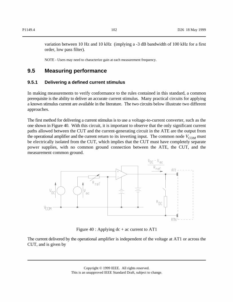
P1149.4 102 D26 18 May 1999
Copyright © 1999 IEEE. All rights reserved.This is an unapproved IEEE Standard Draft, subject to change.
Figure 40 : Applying dc + ac current to AT1
variation between 10 Hz and 10 kHz (implying a -3 dB bandwidth of 100 kHz for a firstorder, low pass filter).
NOTE - Users may need to characterize gain at each measurement frequency.
9.5 Measuring performance
9.5.1 Delivering a defined current stimulus
In making measurements to verify conformance to the rules contained in this standard, a commonprerequisite is the ability to deliver an accurate current stimulus. Many practical circuits for applyinga known stimulus current are available in the literature. The two circuits below illustrate two differentapproaches.
The first method for delivering a current stimulus is to use a voltage-to-current converter, such as theone shown in Figure 40. With this circuit, it is important to observe that the only significant currentpaths allowed between the CUT and the current-generating circuit in the ATE are the output fromthe operational amplifier and the current return to its inverting input. The common node V mustCOMbe electrically isolated from the CUT, which implies that the CUT must have completely separatepower supplies, with no common ground connection between the ATE, the CUT, and themeasurement common ground.
The current delivered by the operational amplifier is independent of the voltage at AT1 or across theCUT, and is given by
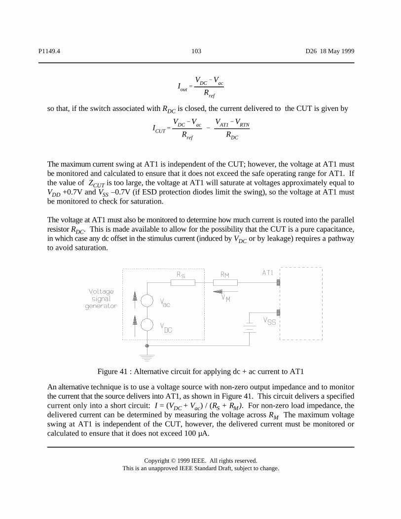
ICUT'VDC&Vac
Rref
&VAT1&VRTN
RDC
Iout'VDC&Vac
Rref
P1149.4 103 D26 18 May 1999
Copyright © 1999 IEEE. All rights reserved.This is an unapproved IEEE Standard Draft, subject to change.
Figure 41 : Alternative circuit for applying dc + ac current to AT1
so that, if the switch associated with R is closed, the current delivered to the CUT is given byDC
The maximum current swing at AT1 is independent of the CUT; however, the voltage at AT1 mustbe monitored and calculated to ensure that it does not exceed the safe operating range for AT1. Ifthe value of Z is too large, the voltage at AT1 will saturate at voltages approximately equal toCUTV +0.7V and V –0.7V (if ESD protection diodes limit the swing), so the voltage at AT1 mustDD SSbe monitored to check for saturation.
The voltage at AT1 must also be monitored to determine how much current is routed into the parallelresistor R . This is made available to allow for the possibility that the CUT is a pure capacitance,DCin which case any dc offset in the stimulus current (induced by V or by leakage) requires a pathwayDCto avoid saturation.
An alternative technique is to use a voltage source with non-zero output impedance and to monitorthe current that the source delivers into AT1, as shown in Figure 41. This circuit delivers a specifiedcurrent only into a short circuit: I = (V + V ) / (R + R ). For non-zero load impedance, theDC ac S Mdelivered current can be determined by measuring the voltage across R The maximum voltageMswing at AT1 is independent of the CUT, however, the delivered current must be monitored orcalculated to ensure that it does not exceed 100 µA.
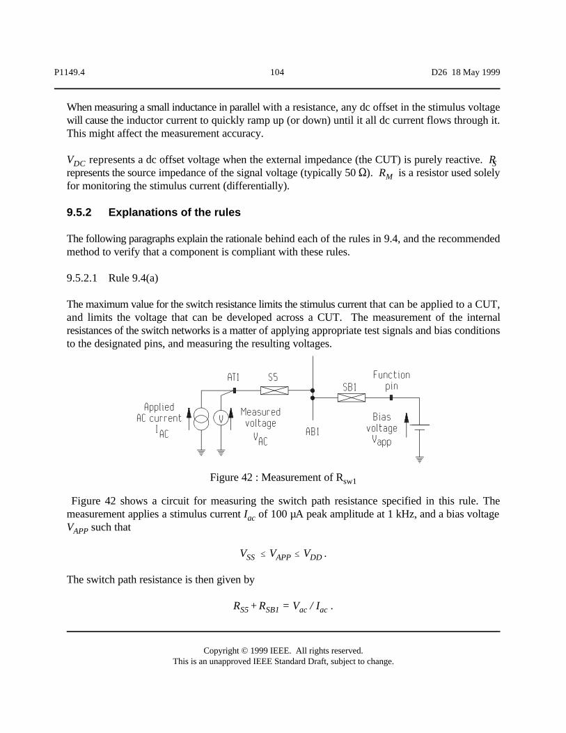
P1149.4 104 D26 18 May 1999
Copyright © 1999 IEEE. All rights reserved.This is an unapproved IEEE Standard Draft, subject to change.
Figure 42 : Measurement of Rsw1
When measuring a small inductance in parallel with a resistance, any dc offset in the stimulus voltagewill cause the inductor current to quickly ramp up (or down) until it all dc current flows through it.This might affect the measurement accuracy.
V represents a dc offset voltage when the external impedance (the CUT) is purely reactive. RDC Srepresents the source impedance of the signal voltage (typically 50 S). R is a resistor used solelyMfor monitoring the stimulus current (differentially).
9.5.2 Explanations of the rules
The following paragraphs explain the rationale behind each of the rules in 9.4, and the recommendedmethod to verify that a component is compliant with these rules.
9.5.2.1 Rule 9.4(a)
The maximum value for the switch resistance limits the stimulus current that can be applied to a CUT,and limits the voltage that can be developed across a CUT. The measurement of the internalresistances of the switch networks is a matter of applying appropriate test signals and bias conditionsto the designated pins, and measuring the resulting voltages.
Figure 42 shows a circuit for measuring the switch path resistance specified in this rule. Themeasurement applies a stimulus current I of 100 µA peak amplitude at 1 kHz, and a bias voltageacV such that APP
V # V # V .SS APP DD
The switch path resistance is then given by
R + R = V / I .S5 SB1 ac ac
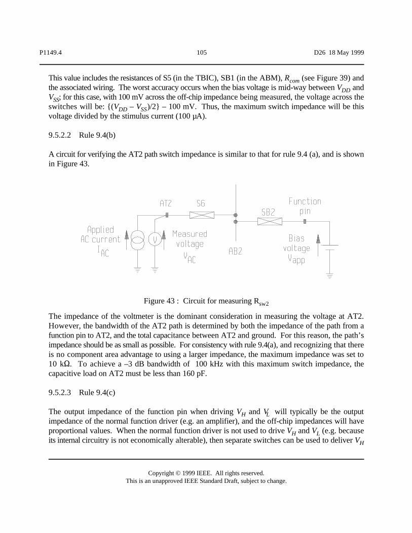
P1149.4 105 D26 18 May 1999
Copyright © 1999 IEEE. All rights reserved.This is an unapproved IEEE Standard Draft, subject to change.
Figure 43 : Circuit for measuring Rsw2
This value includes the resistances of S5 (in the TBIC), SB1 (in the ABM), R (see Figure 39) andcomthe associated wiring. The worst accuracy occurs when the bias voltage is mid-way between V andDDV ; for this case, with 100 mV across the off-chip impedance being measured, the voltage across theSSswitches will be: {(V – V )/2} – 100 mV. Thus, the maximum switch impedance will be thisDD SSvoltage divided by the stimulus current (100 µA).
9.5.2.2 Rule 9.4(b)
A circuit for verifying the AT2 path switch impedance is similar to that for rule 9.4 (a), and is shownin Figure 43.
The impedance of the voltmeter is the dominant consideration in measuring the voltage at AT2.However, the bandwidth of the AT2 path is determined by both the impedance of the path from afunction pin to AT2, and the total capacitance between AT2 and ground. For this reason, the path’simpedance should be as small as possible. For consistency with rule 9.4(a), and recognizing that thereis no component area advantage to using a larger impedance, the maximum impedance was set to10 kS. To achieve a –3 dB bandwidth of 100 kHz with this maximum switch impedance, thecapacitive load on AT2 must be less than 160 pF.
9.5.2.3 Rule 9.4(c)
The output impedance of the function pin when driving V and V will typically be the outputH Limpedance of the normal function driver (e.g. an amplifier), and the off-chip impedances will haveproportional values. When the normal function driver is not used to drive V and V (e.g. becauseH Lits internal circuitry is not economically alterable), then separate switches can be used to deliver VH
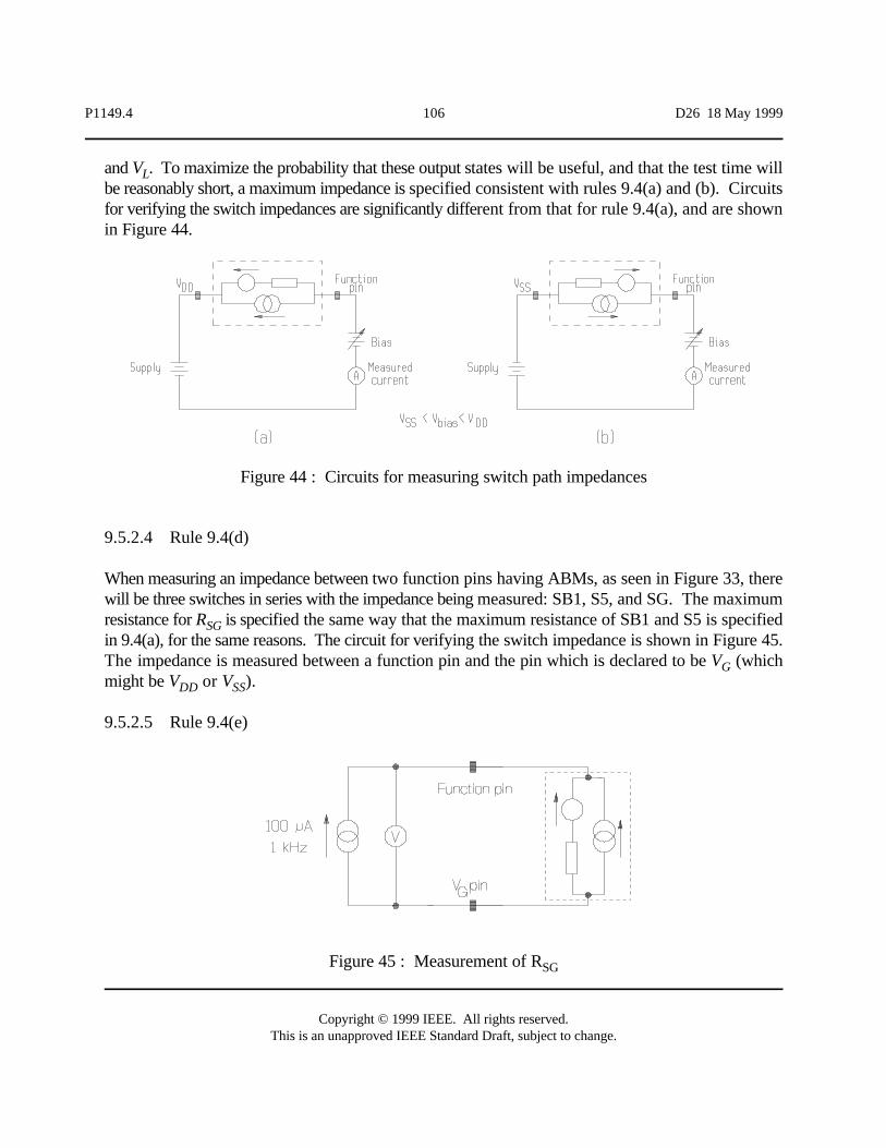
P1149.4 106 D26 18 May 1999
Copyright © 1999 IEEE. All rights reserved.This is an unapproved IEEE Standard Draft, subject to change.
Figure 44 : Circuits for measuring switch path impedances
Figure 45 : Measurement of RSG
and V . To maximize the probability that these output states will be useful, and that the test time willLbe reasonably short, a maximum impedance is specified consistent with rules 9.4(a) and (b). Circuitsfor verifying the switch impedances are significantly different from that for rule 9.4(a), and are shownin Figure 44.
9.5.2.4 Rule 9.4(d)
When measuring an impedance between two function pins having ABMs, as seen in Figure 33, therewill be three switches in series with the impedance being measured: SB1, S5, and SG. The maximumresistance for R is specified the same way that the maximum resistance of SB1 and S5 is specifiedSGin 9.4(a), for the same reasons. The circuit for verifying the switch impedance is shown in Figure 45.The impedance is measured between a function pin and the pin which is declared to be V (whichGmight be V or V ).DD SS
9.5.2.5 Rule 9.4(e)
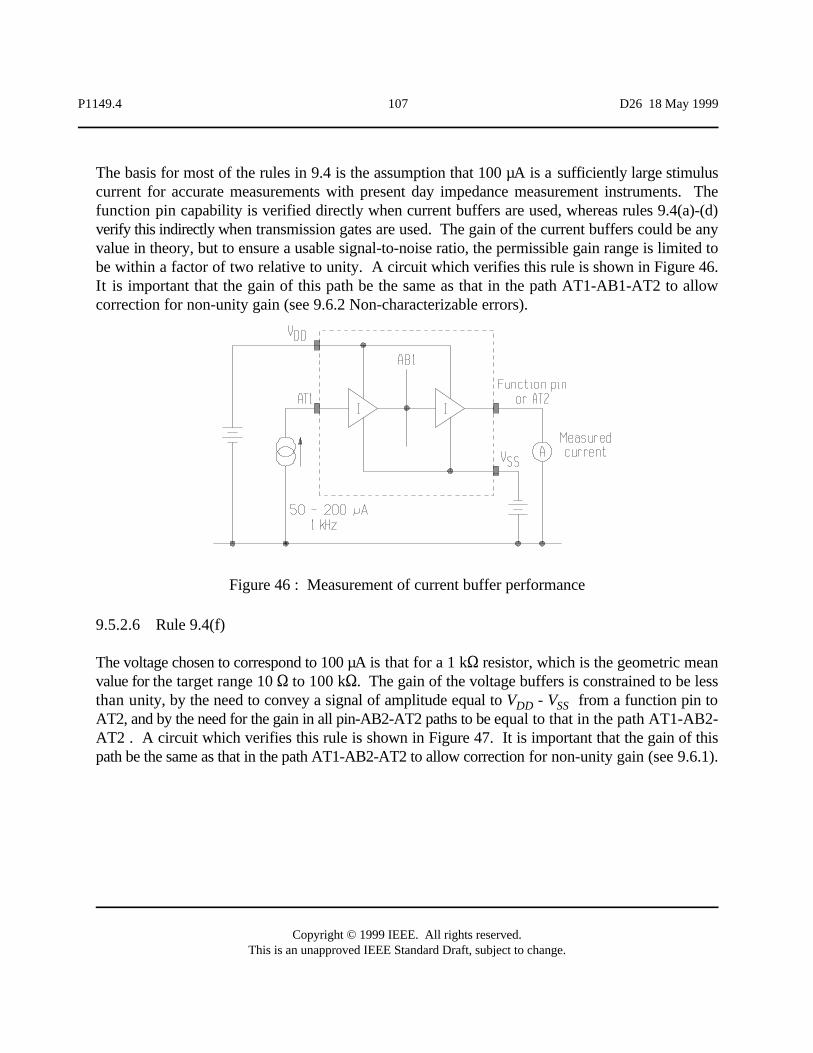
P1149.4 107 D26 18 May 1999
Copyright © 1999 IEEE. All rights reserved.This is an unapproved IEEE Standard Draft, subject to change.
Figure 46 : Measurement of current buffer performance
The basis for most of the rules in 9.4 is the assumption that 100 µA is a sufficiently large stimuluscurrent for accurate measurements with present day impedance measurement instruments. Thefunction pin capability is verified directly when current buffers are used, whereas rules 9.4(a)-(d)verify this indirectly when transmission gates are used. The gain of the current buffers could be anyvalue in theory, but to ensure a usable signal-to-noise ratio, the permissible gain range is limited tobe within a factor of two relative to unity. A circuit which verifies this rule is shown in Figure 46.It is important that the gain of this path be the same as that in the path AT1-AB1-AT2 to allowcorrection for non-unity gain (see 9.6.2 Non-characterizable errors).
9.5.2.6 Rule 9.4(f)
The voltage chosen to correspond to 100 µA is that for a 1 kS resistor, which is the geometric meanvalue for the target range 10 S to 100 kS. The gain of the voltage buffers is constrained to be lessthan unity, by the need to convey a signal of amplitude equal to V - V from a function pin toDD SSAT2, and by the need for the gain in all pin-AB2-AT2 paths to be equal to that in the path AT1-AB2-AT2 . A circuit which verifies this rule is shown in Figure 47. It is important that the gain of thispath be the same as that in the path AT1-AB2-AT2 to allow correction for non-unity gain (see 9.6.1).
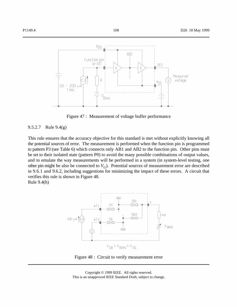
P1149.4 108 D26 18 May 1999
Copyright © 1999 IEEE. All rights reserved.This is an unapproved IEEE Standard Draft, subject to change.
Figure 47 : Measurement of voltage buffer performance
Figure 48 : Circuit to verify measurement error
9.5.2.7 Rule 9.4(g)
This rule ensures that the accuracy objective for this standard is met without explicitly knowing allthe potential sources of error. The measurement is performed when the function pin is programmedto pattern P3 (see Table 6) which connects only AB1 and AB2 to the function pin. Other pins mustbe set to their isolated state (pattern P0) to avoid the many possible combinations of output values,and to emulate the way measurements will be performed in a system (in system-level testing, oneother pin might be also be connected to V ). Potential sources of measurement error are describedGin 9.6.1 and 9.6.2, including suggestions for minimizing the impact of these errors. A circuit thatverifies this rule is shown in Figure 48.Rule 9.4(h)
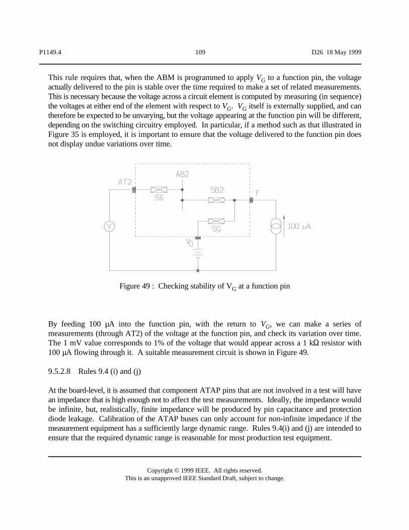
P1149.4 109 D26 18 May 1999
Copyright © 1999 IEEE. All rights reserved.This is an unapproved IEEE Standard Draft, subject to change.
Figure 49 : Checking stability of V at a function pinG
This rule requires that, when the ABM is programmed to apply V to a function pin, the voltageGactually delivered to the pin is stable over the time required to make a set of related measurements.This is necessary because the voltage across a circuit element is computed by measuring (in sequence)the voltages at either end of the element with respect to V . V itself is externally supplied, and canG Gtherefore be expected to be unvarying, but the voltage appearing at the function pin will be different,depending on the switching circuitry employed. In particular, if a method such as that illustrated inFigure 35 is employed, it is important to ensure that the voltage delivered to the function pin doesnot display undue variations over time.
By feeding 100 µA into the function pin, with the return to V , we can make a series ofGmeasurements (through AT2) of the voltage at the function pin, and check its variation over time.The 1 mV value corresponds to 1% of the voltage that would appear across a 1 kS resistor with100 µA flowing through it. A suitable measurement circuit is shown in Figure 49.
9.5.2.8 Rules 9.4 (i) and (j)
At the board-level, it is assumed that component ATAP pins that are not involved in a test will havean impedance that is high enough not to affect the test measurements. Ideally, the impedance wouldbe infinite, but, realistically, finite impedance will be produced by pin capacitance and protectiondiode leakage. Calibration of the ATAP buses can only account for non-infinite impedance if themeasurement equipment has a sufficiently large dynamic range. Rules 9.4(i) and (j) are intended toensure that the required dynamic range is reasonable for most production test equipment.
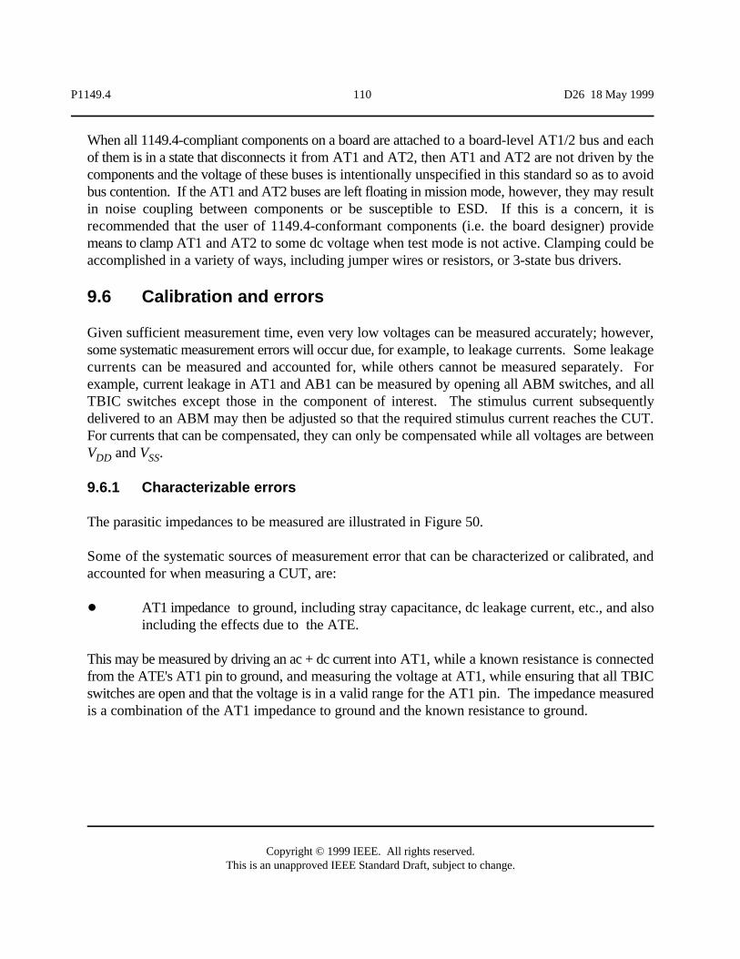
P1149.4 110 D26 18 May 1999
Copyright © 1999 IEEE. All rights reserved.This is an unapproved IEEE Standard Draft, subject to change.
When all 1149.4-compliant components on a board are attached to a board-level AT1/2 bus and eachof them is in a state that disconnects it from AT1 and AT2, then AT1 and AT2 are not driven by thecomponents and the voltage of these buses is intentionally unspecified in this standard so as to avoidbus contention. If the AT1 and AT2 buses are left floating in mission mode, however, they may resultin noise coupling between components or be susceptible to ESD. If this is a concern, it isrecommended that the user of 1149.4-conformant components (i.e. the board designer) providemeans to clamp AT1 and AT2 to some dc voltage when test mode is not active. Clamping could beaccomplished in a variety of ways, including jumper wires or resistors, or 3-state bus drivers.
9.6 Calibration and errors
Given sufficient measurement time, even very low voltages can be measured accurately; however,some systematic measurement errors will occur due, for example, to leakage currents. Some leakagecurrents can be measured and accounted for, while others cannot be measured separately. Forexample, current leakage in AT1 and AB1 can be measured by opening all ABM switches, and allTBIC switches except those in the component of interest. The stimulus current subsequentlydelivered to an ABM may then be adjusted so that the required stimulus current reaches the CUT.For currents that can be compensated, they can only be compensated while all voltages are betweenV and V .DD SS
9.6.1 Characterizable errors
The parasitic impedances to be measured are illustrated in Figure 50.
Some of the systematic sources of measurement error that can be characterized or calibrated, andaccounted for when measuring a CUT, are:
! AT1 impedance to ground, including stray capacitance, dc leakage current, etc., and alsoincluding the effects due to the ATE.
This may be measured by driving an ac + dc current into AT1, while a known resistance is connectedfrom the ATE's AT1 pin to ground, and measuring the voltage at AT1, while ensuring that all TBICswitches are open and that the voltage is in a valid range for the AT1 pin. The impedance measuredis a combination of the AT1 impedance to ground and the known resistance to ground.

P1149.4 111 D26 18 May 1999
Copyright © 1999 IEEE. All rights reserved.This is an unapproved IEEE Standard Draft, subject to change.
Figure 50 : Measurement of parasitic impedance
! AT2 impedance to ground, including stray capacitance, dc leakage current, etc., and alsoincluding the effects due to the ATE.
This may be measured by driving an ac + dc current into AT2, while a known resistance is connectedfrom the ATE's AT2 pin to ground, and measuring the voltage at AT2, while ensuring that all TBICswitches are open and that the voltage is in a valid range for the AT2 pin. The impedance measuredis a combination of the AT2 impedance to ground and the known resistance to ground.
! AB1 impedance (capacitance, dc leakage current, etc.) to ground.
This may be measured by driving an ac + dc current into AT1, while a known resistance is connectedfrom the ATE's AT1 pin to ground, and measuring the voltage at AT2, while enablingAT1-S5-AB1-S8-AT2 on one component and disabling the TBIC switches on all other components.The impedance measured is a combination of the AT1 impedance to ground (measured separately),the AT2 impedance to ground (measured separately), the known resistance, and the AB1 impedanceto ground. ! AB2 impedance (capacitance, dc leakage current, etc.) to ground;
This may be measured by driving an ac + dc current into AT1, while a known resistance is connectedfrom the ATE's AT1 pin to ground, and measuring the voltage at AT2, while enablingAT1-S5-AB1-S8-AT2 on one component and disabling the TBIC switches on all other components.
P1149.4 112 D26 18 May 1999
Copyright © 1999 IEEE. All rights reserved.This is an unapproved IEEE Standard Draft, subject to change.
The impedance measured is a combination of the AT1 impedance to ground (measured separately),the AT2 impedance to ground (measured separately), the known resistance, and the AB1 impedanceto ground. ! Voltage buffer gain
When voltage buffers are used within the component for the AB2/AT2 path, the gain may bemeasured similarly to the method in rule (g), except that the resistor measured is connected to AT1instead of a function pin. The gain is the ratio of the acvoltage observed at AT2 to the voltageobserved at AT1, when using a high impedance voltmeter, and enabling the AT1-S7-AB2-S6-AT2path. This does not, however, characterize any buffers used for the function pin ABM switches (see9.6.2 Non-characterizable errors).
! Current buffer gain.
When current buffers are used within the component for the AB1/AT1 path, the gain may bemeasured similarly to the method in rule (g), except that the resistor measured is connected to AT2instead of a function pin. The gain is the ratio of the acvoltage observed at AT2 to the acstimuluscurrent delivered into AT1, divided by the resistor's value, when using a high impedance voltmeter,and enabling the AT1-S5-AB1-S8-AT2 path. This does not, however, characterize any buffers usedfor the function pin ABM switches (see 9.6.2 Non-characterizable errors).
! VTH
The threshold voltages used as a reference by the comparator in each ABM can be determined bymonitoring the voltage at each pin, via AB2 and AT2, and the relevant ABM register bit valuecaptured and shifted out during boundary scan. This method is only applicable when the voltage atthe pin of interest is not varying significantly.
Note that the above measurements are described assuming a current-based driver such as that inFigure 40. The measurements can also be performed using a voltage-based driver such as that inFigure 41.
9.6.2 Non-characterizable errors
Some parameters of the mixed-signal test infra-structure are not measurable after the component hasbeen embedded in the application circuit board because the external circuitry connected to thefunction pin will influence any measurement of the on-chip parameters unpredictably. These
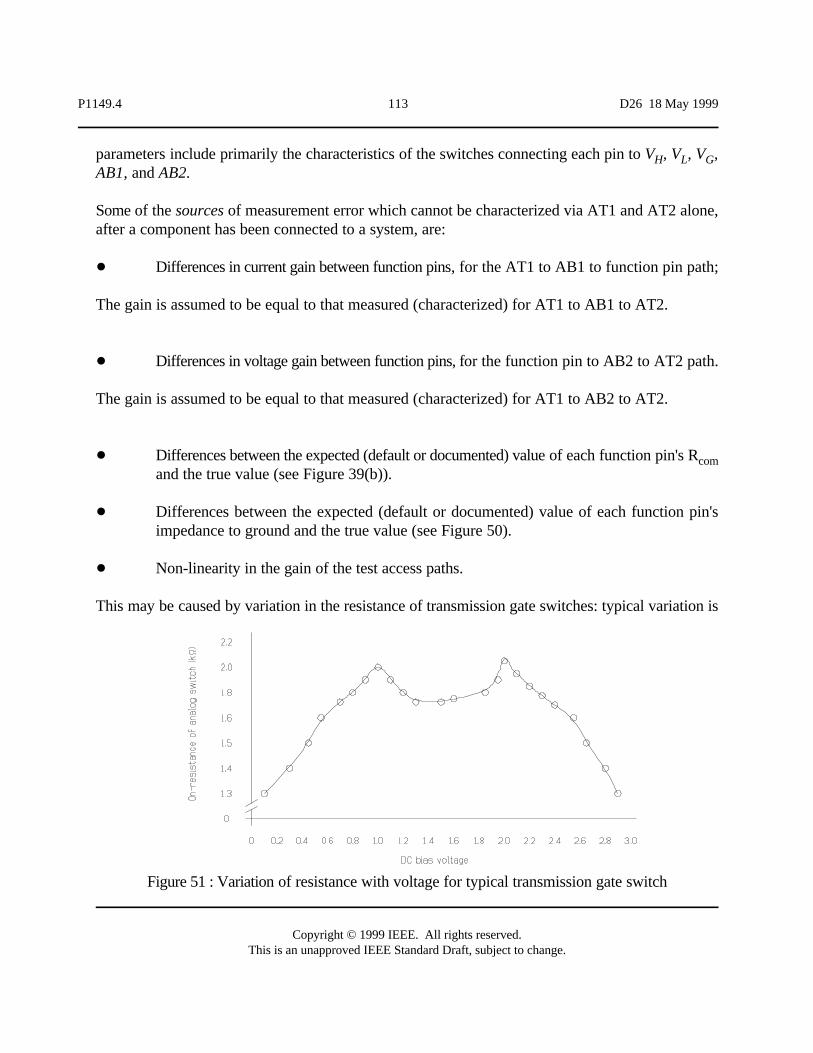
P1149.4 113 D26 18 May 1999
Copyright © 1999 IEEE. All rights reserved.This is an unapproved IEEE Standard Draft, subject to change.
Figure 51 : Variation of resistance with voltage for typical transmission gate switch
parameters include primarily the characteristics of the switches connecting each pin to V , V , V ,H L GAB1, and AB2.
Some of the sources of measurement error which cannot be characterized via AT1 and AT2 alone,after a component has been connected to a system, are:
! Differences in current gain between function pins, for the AT1 to AB1 to function pin path;
The gain is assumed to be equal to that measured (characterized) for AT1 to AB1 to AT2.
! Differences in voltage gain between function pins, for the function pin to AB2 to AT2 path.
The gain is assumed to be equal to that measured (characterized) for AT1 to AB2 to AT2.
! Differences between the expected (default or documented) value of each function pin's Rcomand the true value (see Figure 39(b)).
! Differences between the expected (default or documented) value of each function pin'simpedance to ground and the true value (see Figure 50).
! Non-linearity in the gain of the test access paths.
This may be caused by variation in the resistance of transmission gate switches: typical variation is

P1149.4 114 D26 18 May 1999
Copyright © 1999 IEEE. All rights reserved.This is an unapproved IEEE Standard Draft, subject to change.
shown in Figure 51. Reducing the ac voltage or current amplitude can reduce non-linearity, but alsodecreases the signal to noise ratio.
! Noise;
Integrating over a longer period of time can reduce thermal and switching noise to arbitrarily lowvalues. 1/f noise can be reduced by measuring at frequencies greater than 100 Hz.
P1149.4 115 D26 18 May 1999
Copyright © 1999 IEEE. All rights reserved.This is an unapproved IEEE Standard Draft, subject to change.
10 Conformance and Documentation
10.1 Conformance
10.1.1 Specification
Rule
(a) A component claiming conformance with this standard shall comply with all the rules setout herein.
NOTE 1 - By virtue of the rules contained in 4.1, this requires that the component shall also comply with themajority of the rules of IEEE Std 1149.1.
NOTE 2 - In accordance with the rules of IEEE Std 1149.1, a component may be supplied with one or morecompliance-enable pins such that full compliance with the rules of this standard is assured only when a definedpattern of enable signals is applied to the compliance-enable pin(s).
NOTE 3 - There may be more than one compliance-enable pattern.
10.2 General documentation
To allow the user to make use of the facilities included in a component, a range of information hasto be made available by the manufacturer. This clause identifies the minimum data that must beprovided for a component that conforms to this standard.
10.2.1 Transmission pathways
A key function of the structures described in this standard is to apply voltages and currents tofunction pins. This involves the use of switch pathways which, in practice, will be imperfect. Thecharacteristics of these pathways can be defined by a model, together with the limits of operatingconditions under which the model is valid.
Figure 52 shows a model that will be used to describe each of the switch pathways supplying avoltage (V , V , or V ) to a function pin through its ABM. Note that the model takes no accountH L Gof residual elements that remain connected to the function pin while in test mode; these are describedseparately.
In this model, which is intended to provide a good first-order approximation to the behavior of thepathway over a stated range of operating conditions, the supplied voltage (any of V , V or V ) isH L G
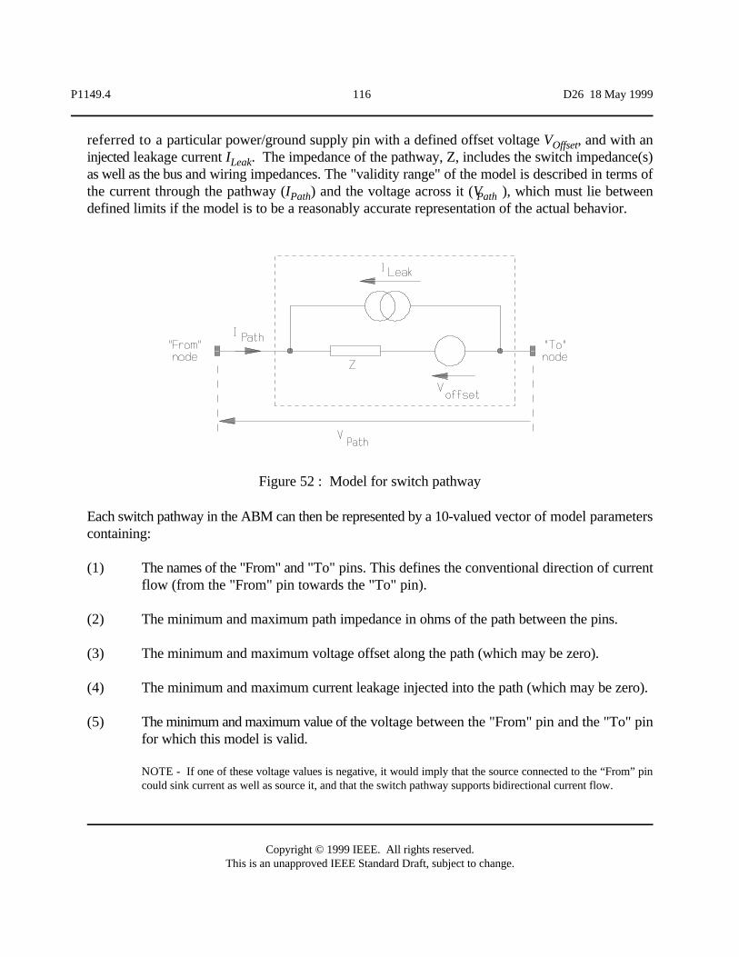
P1149.4 116 D26 18 May 1999
Copyright © 1999 IEEE. All rights reserved.This is an unapproved IEEE Standard Draft, subject to change.
Figure 52 : Model for switch pathway
referred to a particular power/ground supply pin with a defined offset voltage V , and with anOffsetinjected leakage current I . The impedance of the pathway, Z, includes the switch impedance(s)Leakas well as the bus and wiring impedances. The "validity range" of the model is described in terms ofthe current through the pathway (I ) and the voltage across it (V ), which must lie betweenPath Pathdefined limits if the model is to be a reasonably accurate representation of the actual behavior.
Each switch pathway in the ABM can then be represented by a 10-valued vector of model parameterscontaining:
(1) The names of the "From" and "To" pins. This defines the conventional direction of currentflow (from the "From" pin towards the "To" pin).
(2) The minimum and maximum path impedance in ohms of the path between the pins.
(3) The minimum and maximum voltage offset along the path (which may be zero).
(4) The minimum and maximum current leakage injected into the path (which may be zero).
(5) The minimum and maximum value of the voltage between the "From" pin and the "To" pinfor which this model is valid.
NOTE - If one of these voltage values is negative, it would imply that the source connected to the “From” pincould sink current as well as source it, and that the switch pathway supports bidirectional current flow.
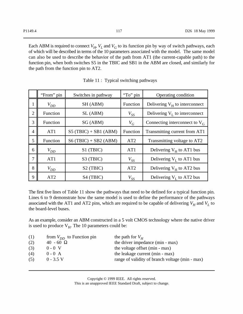
P1149.4 117 D26 18 May 1999
Copyright © 1999 IEEE. All rights reserved.This is an unapproved IEEE Standard Draft, subject to change.
“From” pin Switches in pathway “To” pin Operating condition
1 VDD SH (ABM) Function Delivering V to interconnectH
2 Function SL (ABM) VSS Delivering V to interconnectL
3 Function SG (ABM) VG Connecting interconnect to VG
4 AT1 S5 (TBIC) + SB1 (ABM) Function Transmitting current from AT1
5 Function S6 (TBIC) + SB2 (ABM) AT2 Transmitting voltage to AT2
6 VDD S1 (TBIC) AT1 Delivering V to AT1 busH
7 AT1 S3 (TBIC) VSS Delivering V to AT1 busL
8 VDD S2 (TBIC) AT2 Delivering V to AT2 busH
9 AT2 S4 (TBIC) VSS Delivering V to AT2 busL
Table 11 : Typical switching pathways
Each ABM is required to connect V , V and V to its function pin by way of switch pathways, eachH L Gof which will be described in terms of the 10 parameters associated with the model. The same modelcan also be used to describe the behavior of the path from AT1 (the current-capable path) to thefunction pin, when both switches S5 in the TBIC and SB1 in the ABM are closed, and similarly forthe path from the function pin to AT2.
The first five lines of Table 11 show the pathways that need to be defined for a typical function pin.Lines 6 to 9 demonstrate how the same model is used to define the performance of the pathwaysassociated with the AT1 and AT2 pins, which are required to be capable of delivering V and V toH Lthe board-level buses.
As an example, consider an ABM constructed in a 5 volt CMOS technology where the native driveris used to produce V . The 10 parameters could be:H
(1) from V to Function pin the path for VDD H(2) 40 - 60 S the driver impedance (min - max)(3) 0 - 0 V the voltage offset (min - max)(4) 0 - 0 A the leakage current (min - max)(5) 0 - 3.5 V range of validity of branch voltage (min - max)
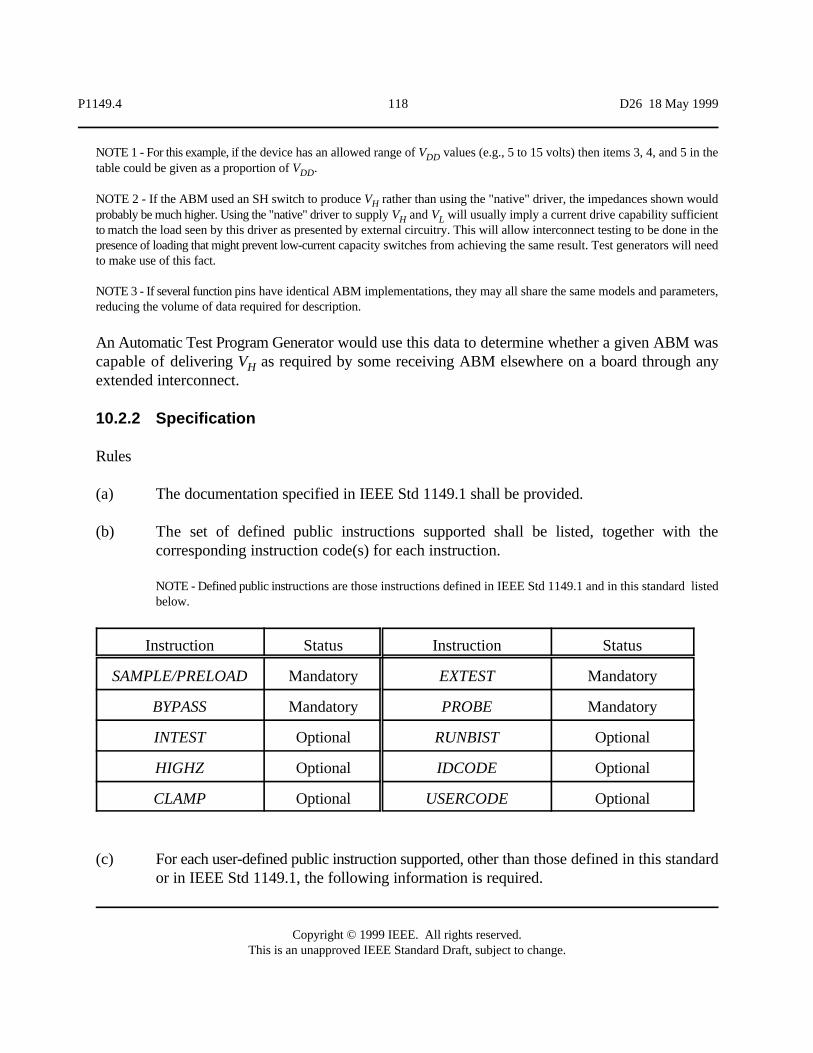
P1149.4 118 D26 18 May 1999
Copyright © 1999 IEEE. All rights reserved.This is an unapproved IEEE Standard Draft, subject to change.
NOTE 1 - For this example, if the device has an allowed range of V values (e.g., 5 to 15 volts) then items 3, 4, and 5 in theDDtable could be given as a proportion of V .DD
NOTE 2 - If the ABM used an SH switch to produce V rather than using the "native" driver, the impedances shown wouldHprobably be much higher. Using the "native" driver to supply V and V will usually imply a current drive capability sufficientH Lto match the load seen by this driver as presented by external circuitry. This will allow interconnect testing to be done in thepresence of loading that might prevent low-current capacity switches from achieving the same result. Test generators will needto make use of this fact.
NOTE 3 - If several function pins have identical ABM implementations, they may all share the same models and parameters,reducing the volume of data required for description.
An Automatic Test Program Generator would use this data to determine whether a given ABM wascapable of delivering V as required by some receiving ABM elsewhere on a board through anyHextended interconnect.
10.2.2 Specification
Rules
(a) The documentation specified in IEEE Std 1149.1 shall be provided.
(b) The set of defined public instructions supported shall be listed, together with thecorresponding instruction code(s) for each instruction.
NOTE - Defined public instructions are those instructions defined in IEEE Std 1149.1 and in this standard listedbelow.
Instruction Status Instruction Status
SAMPLE/PRELOAD Mandatory EXTEST Mandatory
BYPASS Mandatory PROBE Mandatory
INTEST Optional RUNBIST Optional
HIGHZ Optional IDCODE Optional
CLAMP Optional USERCODE Optional
(c) For each user-defined public instruction supported, other than those defined in this standardor in IEEE Std 1149.1, the following information is required.
P1149.4 119 D26 18 May 1999
Copyright © 1999 IEEE. All rights reserved.This is an unapproved IEEE Standard Draft, subject to change.
(i) The binary code(s) for the instruction.
(ii) A list of test data registers affected by the instruction.
(iii) The name of the serial test data register path selected by the instruction to beconnected between TDI and TDO.
(iv) A definition of the purpose of the instruction, the method of performing the test,the test data register(s) that will hold the results of the test, and the way in whichthese results are to be examined.
(d) If private instructions are utilized in a component, the vendor shall clearly identify anyinstruction codes that, if selected, would cause hazardous or unpredictable operation of thecomponent.
(e) For each ABM attached to a function pin, the following data shall be supplied.
(i) The behavior of the boundary module, including signals captured by uncommittedcapture flip-flop inputs used to improve ABM testability.
(ii) The positioning of the control bits within the boundary-scan register.
(iii) The value and tolerance of V .TH
NOTE - If there is a non-zero tolerance on V , this indicates that a portion of the voltage rangeTHbetween V and V cannot be used to resolve a signal voltage into a digital bit. H L
(iv) A set of 10 model parameters for each of the pathways associated with V .V ,G, HV , AT1, and AT2.L
(f) For the TBIC, the following data shall be supplied.
(i) The behavior of the boundary module, including signals captured by uncommittedcapture flip-flop inputs used to improve TBIC testability.
(ii) The partitioning (if any) of the internal test bus structure.
(iii) The number of partitions.
P1149.4 120 D26 18 May 1999
Copyright © 1999 IEEE. All rights reserved.This is an unapproved IEEE Standard Draft, subject to change.
(iv) The allocation of ABMs to partitions.
(v) The positioning of the control bits within the boundary-scan register.
(vi) The value and tolerance of V .TH
NOTE - If there is a non-zero tolerance on V , this indicates that a portion of the voltage rangeTHbetween V and V cannot be used to resolve a signal voltage into a digital bit. H L
(vii) A set of 10 model parameters for each of the pathways involved with deliveringV and V to AT1 and AT2.H L
(g) If a differential ATAP is included in the component, documentation relating to AT1N andAT2N shall be provided in the same form as that for AT1 and AT2 respectively.
10.3 Documentation of residual elements
10.3.1 Specification
Rules
(a) Any circuit network that remains connected to the function pins when the component is inCD mode shall be modeled as a network of residual elements, and described in a ResidualElement Table.
NOTE 1 - Residual elements may be connected from function pins to power pins, other function pins, or otherresidual elements (see 7.3.3).
NOTE 2 - The Residual Element Table will be used to account for common series resistance in the metalization,pad, bond wire and lead frame between a device pin and the ABM (R in Figure 39(b)), as well as the effectscomof significant capacitance to ground that may exist.
NOTE 3 - The value of R always needs to be documented, since even a value of less than 1S can produce errorscomof more than 1% when measuring some impedances within the stated target range (10S to 100 kS).
NOTE 4 - If analog pins have a common design "footprint" a single general model may suffice to document theseries impedance and capacitance to ground for all the analog pins. This model could be based on Figure 52,noting that, in some cases, the values of resistance may be zero and/or the capacitance may be small enough toignore.
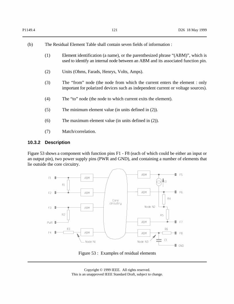
P1149.4 121 D26 18 May 1999
Copyright © 1999 IEEE. All rights reserved.This is an unapproved IEEE Standard Draft, subject to change.
Figure 53 : Examples of residual elements
(b) The Residual Element Table shall contain seven fields of information :
(1) Element identification (a name), or the parenthesized phrase “(ABM)”, which isused to identify an internal node between an ABM and its associated function pin.
(2) Units (Ohms, Farads, Henrys, Volts, Amps).
(3) The “from” node (the node from which the current enters the element : onlyimportant for polarized devices such as independent current or voltage sources).
(4) The “to” node (the node to which current exits the element).
(5) The minimum element value (in units defined in (2)).
(6) The maximum element value (in units defined in (2)).
(7) Match/correlation.
10.3.2 Description
Figure 53 shows a component with function pins F1 - F8 (each of which could be either an input oran output pin), two power supply pins (PWR and GND), and containing a number of elements thatlie outside the core circuitry.
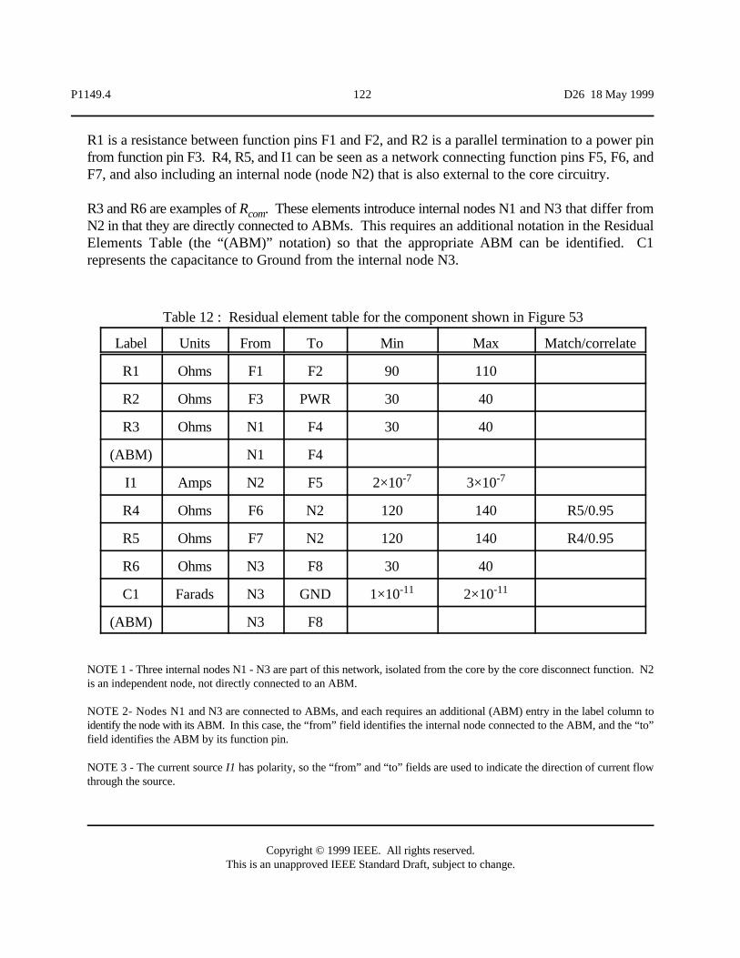
P1149.4 122 D26 18 May 1999
Copyright © 1999 IEEE. All rights reserved.This is an unapproved IEEE Standard Draft, subject to change.
Label Units From To Min Max Match/correlate
R1 Ohms F1 F2 90 110
R2 Ohms F3 PWR 30 40
R3 Ohms N1 F4 30 40
(ABM) N1 F4
I1 Amps N2 F5 2×10⁻⁷ 3×10⁻⁷
R4 Ohms F6 N2 120 140 R5/0.95
R5 Ohms F7 N2 120 140 R4/0.95
R6 Ohms N3 F8 30 40
C1 Farads N3 GND 1×10-11 2×10-11
(ABM) N3 F8
Table 12 : Residual element table for the component shown in Figure 53
R1 is a resistance between function pins F1 and F2, and R2 is a parallel termination to a power pinfrom function pin F3. R4, R5, and I1 can be seen as a network connecting function pins F5, F6, andF7, and also including an internal node (node N2) that is also external to the core circuitry.
R3 and R6 are examples of R . These elements introduce internal nodes N1 and N3 that differ fromcomN2 in that they are directly connected to ABMs. This requires an additional notation in the ResidualElements Table (the “(ABM)” notation) so that the appropriate ABM can be identified. C1represents the capacitance to Ground from the internal node N3.
NOTE 1 - Three internal nodes N1 - N3 are part of this network, isolated from the core by the core disconnect function. N2is an independent node, not directly connected to an ABM.
NOTE 2- Nodes N1 and N3 are connected to ABMs, and each requires an additional (ABM) entry in the label column toidentify the node with its ABM. In this case, the “from” field identifies the internal node connected to the ABM, and the “to”field identifies the ABM by its function pin.
NOTE 3 - The current source I1 has polarity, so the “from” and “to” fields are used to indicate the direction of current flowthrough the source.
P1149.4 123 D26 18 May 1999
Copyright © 1999 IEEE. All rights reserved.This is an unapproved IEEE Standard Draft, subject to change.
Residual elements are those that cannot be disconnected from the pins by the core disconnectfunction, and that therefore must be documented in a Residual Element Table. This table also, as amatter of convenience, includes elements that lie in series between the ABM and the pin (such as Rcomin Figure 39(b)) : such series impedances are often associated with ESD protection circuitry and bondwires. Some portion of ESD protection circuitry (such as reverse-biased clamp diodes) do not needto be documented because they will not conduct current during normal testing activities; seriesimpedances will need to be documented.
Each element, regardless of how it is implemented, must be characterized by a model containing onlyR, L, C, and independent V and I elements.
The match/correlation field for a particular element may be empty, or it may contain a list of elementidentification labels that are matched to this element, along with a specified correlation between - 1.0and +1.0. This is used to identify groups of residual elements whose values are matched such thattheir variations (between min and max) are correlated and not independent.
The residual element table for the component of Figure 53 is shown in Table 12.


![HMO2024 - SOS · [HMO2024] HMO1522 [HMO1524], Mixed Signal Mixed Signal 2](https://static.fdocuments.in/doc/165x107/606a26e1cd05047284562add/hmo2024-sos-hmo2024-hmo1522-hmo1524-mixed-signal-mixed-signal-2.jpg)