DPOJET Opt. PCE PCI Express Measurements & Setup Library · DPOJET Opt. PCE PCI Express...
35
Technical Reference www.tektronix.com DPOJET Opt. PCE PCI Express Measurements & Setup Library Methods of Implementation (MOI) for Verification, Debug and Characterization 077-0267-00
Transcript of DPOJET Opt. PCE PCI Express Measurements & Setup Library · DPOJET Opt. PCE PCI Express...

Technical Reference
www.tektronix.com
DPOJET Opt. PCE
PCI Express Measurements & Setup Library
Methods of Implementation (MOI) for Verification, Debug and Characterization
077-0267-00

DPOJET PCI Express MOI Page ii of 35
Copyright © Tektronix. All rights reserved. Licensed software products are owned by Tektronix or its suppliers
and are protected by United States copyright laws and international treaty provisions.
Tektronix products are covered by U.S. and foreign patents, issued and pending. Information in this publication
supercedes that in all previously published material. Specifications and price change privileges reserved.
TEKTRONIX, TEK and RT-Eye are registered trademarks of Tektronix, Inc.
Contacting Tektronix
Tektronix, Inc.
14200 SW Karl Braun Drive or P.O. Box 500
Beaverton, OR 97077 USA
For product information, sales, service, and technical support:
In North America, call 1-800-833-9200.
Worldwide, visit www.tektronix.com to find contacts in your area.

Methods of Implementation
DPOJET PCI Express Measurements 1
Table of Contents
1 Introduction to the DPOJET PCI Express Setup Library .................... 2
2 PCI Express Specifications ....................................................................... 3
2.1 Differential Transmitter (TX) Output Specifications.............................3
2.2 Differential Receiver (RX) Input Specifications .....................................3
2.3 Add-In Card Transmitter Path Compliance Specifications ..................5
2.4 System Board Transmitter Path Specifications ......................................7
2.5 PCI ExpressModule™ Specifications ......................................................9
2.6 PCI Express External Cabling Specifications .......................................12
2.7 PCMCIA ExpressCardTM
Specifications ...............................................14
3 PCI Express Library Contents............................................................... 16
4 Preparing to Take Measurements.......................................................... 17
4.1 Required Equipment ...............................................................................17
4.2 Probing Options for Transmitter Testing..............................................18
SMA Input Connection ...........................................................................18
ECB pad connection ................................................................................19
Dual Port Connection ..............................................................................20
4.3 Running the Test......................................................................................21
5 Parameter Definitions and Method of implementation ....................... 23
5.1 UI (Unit Interval) MOI............................................................................23
5.2 TX Differential Pk-Pk Output Voltage MOI.........................................24
5.3 TX De-Emphasis Ratio............................................................................25
5.4 TX Minimum Pulse Width MOI ............................................................26
5.5 TX Rise/Fall Time Mismatch MOI ........................................................27
5.6 Minimum TX Eye Width MOI...............................................................28
5.7 TX Median-to-Max Jitter MOI ..............................................................29

Methods of Implementation
DPOJET PCI Express MOI Page 2 of 35
1 Introduction to the DPOJET PCI Express Setup Library1 This document provides the procedures for making PCI Express measurements with Tektronix
DPO/DSA70000 Series Oscilloscopes with DPOJET (Jitter and Eye Analysis Tools) and probing solutions.
DPOJET and its PCI Express Setup Library provide transmitter path measurements (amplitude, timing, and
jitter), waveform mask, and limits testing described in multiple variants of the PCI Express specifications.
Table 1 – Supported Specifications in the DPOJET Setup Library
Test Methods Spec Revision
PCI Express Specification Title Test Points Defined
Rev 1.1 Base Specification Transmitter & Receiver
(Section 4.3)
Rev 1.1 CEM Specification System and Add-In Card
(Section 4.7)
Reference Clock (Section 2.1)
Rev 1.0 Express Module Specification Transmitter Path and System Board (Section 5.4)
Rev1.1
Rev 1.0 PCMCIA Express Card Standard Host System Transmitter
Express Card Transmitter
(Section 4.2.1.2)
Rev 1.0 External Cabling Specification Transmitter and Receiver Path (Section 3.3)
Rev 2.0 Base Specification Transmitter & Receiver
(Section 4.4)
Mobile Low Power Transmitter (Section 4.4)
Rev2.0
Rev 2.0 CEM Specification System and Add-In Card (3.5 & 6dB DeEmphasis)
(Section 4.7)
Rev3.0
Rev 0.5 Base Specification Transmitter
(Section 4.1.2)
Refer to http://www.pcisig.com/specifications/pciexpress/ for the latest specifications.
1 Disclaimer: The tests provided in DPOJET (which are described in this document) do not guarantee PCI Express compliance. The test results
should be considered “Pre-Compliance”. Official PCI Express compliance and PCI-SIG Integrator List qualification is governed by the PCI-SIG
(Special Interest Group) and can be achieved only through official PCI-SIG sanctioned testing.
Methods of Implementation
Page 3 of 35
In this document, for all references to the PCI Express Base Specifications and Card Electrical Mechanical
(CEM) specifications, refer to all versions of the Spec. (Rev 1.1, 2.0, and 3.0). Differences between the
specifications are specifically called out when appropriate.
In the subsequent sections, step-by-step procedures are described to help you perform PCI Express
measurements. Each measurement is described as a Method of Implementation (MOI). For further
reference, consult the Compliance checklists and tools offered to PCI-SIG members at www.pcisig.com.
2 PCI Express Specifications As shown in Table 1, Electrical Specifications for PCI Express are provided in multiple documents. This
section provides a summary of the measurement parameters measured in the DPOJET Setup Library module
and how they are related to the symbol and test limits in the specification.
2.1 Differential Transmitter (TX) Output Specifications
The following table shows the available measurements in the PCE Module and their test limits
defined in each of the Base Specifications.
Table 2- Supported Base Specification transmitter measurements
Specification
Parameter Symbol(s)
DPOJET
Measurement 2.5GT/s
Rev1.1/Rev2.0 5.0 GT/s Rev2.0
8.0 GT/s Rev3.0
Clock Recovery NA See Setup by Data Rate >> 1st Order PLL
Fc: 1MHz
Emulates 1st Order filter at
1.5MHz with 75% edge density of Compliance Pattern
2nd Order PLL CDR w/ .707 Damping
Fc: 1.0MHz
- And -
3rd Order LPF
Fc: 1.5MHz
Emulates Step Function Filter at
1.5MHz
1st Order PLL
Fc: 10MHz
Assumes Scrambled Compliance
Pattern with 50% Edge Density
Unit interval UI PCIe UI
(min/max)
SSC filtered with 3rd order HPF: Fc = 198kHz
399.98 (min)
400.12 (max)
199.94 (min)
200.06 (max)
124.9625 (min)
125.0375 (max)
Differential p-p TX voltage swing
pDIFFpTXV−−
VTX-SWING
VTX-EYE-FULL
PCIe T-Tx-Diff-PP
Eye Height
0.8 V (min)
1.2 V (max)
0.8 V (min)
1.2 V (max)
TBD
1.2 V (max)
Low power differential p-p TX voltage swing
VTX-SWING-LOW
VTX-EYE-HALF
PCIe T-Tx-Diff-PP
Eye Height
Not Specified 0.4 V (min)
0.7 V (max)
0.1 V (min)
0.8 V (max)
De-emphasized output voltage ratio
RATIODETXV−−
PCIe T/nT Ratio
-3.0 dB (min)
-4.0 dB (max)
-5.5 dB (min) -6.5 dB (max)
or -3.0 dB (min) -4.0 dB (max)
Not Specified

Methods of Implementation
DPOJET PCI Express MOI Page 4 of 35
Specification
Parameter Symbol(s)
DPOJET
Measurement 2.5GT/s
Rev1.1/Rev2.0 5.0 GT/s Rev2.0
8.0 GT/s Rev3.0
Instantaneous lane pulse width
TMIN-PULSE PCIe Tmin-Pulse Not Specified 0.9UI (min)
150 ps (min)
Not Specified
Transmitter eye including all jitter sources
EYETXT−
tTX-EYE_TJ
For Rev1.1: Eye Width
For Rev2/3: PCIe T-TXA
.75 UI (min)
300 ps (min)
.75 UI (min)
150 ps (min)
TBD
Maximum time between the jitter median and maximum deviation from the median
TTX-EYEMEDIAN-to-
MAXJITTER
PCIe Med-Mx Jitter
.125 UI (min/max)
Not Specified Not Specified
Deterministic jitter TTX-DJ-DD DJ–δδ
Not Specified 0.15 UI (max)
30 ps (max)
TBD
Tx RMS jitter < 1.5MHz
TTX-LF-RMS TIE1 Jitter w/ 3rd Order LPF Fc: 1.5 MHz Std. Deviation
Not Specified 3.0 ps (max) Not Specified
D+/D- TX output rise/fall Time 2
RISETXT−
FALLTXT−
PCIe T-Tx-Rise
PCIe T-Tx-Fall
0.125 UI (min)
50 ps (min)
0.15 UI (min)
30 ps (min)
Not Specified
Tx rise/fall
mismatch TRF-MISMATCH PCIe T-RF-Mismch Not Specified 0.1 UI (max) Not Specified
AC common mode output voltage
VTX-CM-AC-PP Common Mode
Pk-Pk
Not Specified 100 mV (max) 100 mV (max)
AC common mode output voltage
VTX-CM-AC-P Common Mode
Rev1.1 : StdDev
20mV RMS
(max)
Not Specified 20mV RMS
(max)
Absolute delta of DC common mode voltage between D+ and D-
DELTALINEDCCMTXV−−−−
Common Mode
Mean
0 V (min)
25 mV (max)
0 V (min)
25 mV (max)
0 V (min)
25 mV (max)
2 Rise/Fall time measurements in DPOJET are compliant to the Rev1.0a and Rev1.1 specification. For Gen2, rise and fall
time is limited to TF2 and TR2 as defined in section 4.3.3.8 of the Base Specification

Methods of Implementation
DPOJET PCI Express MOI Page 2 of 35
Differential Transmitter (TX) Compliance Eye Diagrams
Figure 1a shows the eye mask definitions for the Rev1.1 Base specification. It provides an example
of a transmitter mask for a signal with de-emphasis. Transition and non-transition bits must be
separated to perform the mask testing. The amplitude and jitter mask geometries are derived from
the amplitude and jitter specifications. Low power transmitter variants in both Gen1 and Gen2 do
not use de-emphasis (This is shown in Figure 1b).
Rev1.1/2.0 Transmitter eye masks for transition and non-transition bits
Rev1.1/2.0 transmitter eye mask for low power variant where de-emphasis is not used
Rev3.0 transmitter eye mask definition – Mask Geometries TBD for Gen3.
Figure 1: PCI Express Transmitter Eye Mask Definitions
Normalized Time (UI)
Pass
Fail
Fail
Fail
Voltage
Y1 Y2
X10.0 1.0
2
1X1−
2
1X1−

Methods of Implementation
Page 3 of 35
2.2 Differential Receiver (RX) Input Specifications
The following table shows the available measurements in the PCE Module and their test limits
defined in each of the Base specifications.
Table 3 – Supported base specification receiver measurements
Parameter Symbol
DPOJET
Measurement
2.5GT/s
Rev1.1/Rev2.0
5.0 GT/s
Rev2.0
8.0 GT/s
Rev3.0
Clock Recovery NA See Setup by Data Rate >> 1st Order PLL
Fc: 1MHz
Emulates 1st Order filter at 1.5MHz with 75% edge density of Compliance Pattern
2nd Order PLL CDR w/ .707 Damping
Fc: 1.0MHz
- And -
3rd Order LPF
Fc: 1.5MHz
Emulates Step Function Filter at
1.5MHz
1st Order PLL
Fc: 10MHz
Assumes Scrambled Compliance Pattern with 50% Edge Density
Unit interval UI PCIe UI
(min/max)
SSC filtered with 3rd order HPF: Fc = 198kHz
399.98 (min)
400.12 (max)
199.94 (min)
200.06 (max)
124.9625 (min)
125.0375 (max)
Minimum receiver eye height VRX_EYE PCIe T-Tx-Diff-PP
Eye Height
.175 V (min)
1.2 V (max)
.120 V (min)
1.2 V (max)
.120 V (min)
1.2 V (max)
Minimum receiver eye width EYERXT
− For Rev1.1: Eye Width
For Rev2/3: Width@BER
.40 UI (min)
160ps (min)
.40 UI (min)
80ps (min)
TBD
Receiver deterministic jitter –Dj
TRX_DJ_DD DJ–δδ Not Specified .44 UI (max)
88ps (max)
TBD
Minimum width
pulse at Rx
TRX-MIN-PULSE PCIe Tmin-Pulse Not Specified .60 UI (min)
120ps (max)
Not Specified
Maximum time between the jitter median and maximum deviation from the median.
TTX-EYEMEDIAN-to-
MAXJITTER PCIe Med-Mx Jitter
.30 UI (max) Not
Specified
Not
Specified
Rx AC common
mode voltage
VRX-CM-AC-P Common Mode
Rev2/3 : Pk-Pk
150mV 150mV Not Spedified

Methods of Implementation
DPOJET PCI Express MOI Page 4 of 35
Differential Receiver (RX) Eye Diagrams
Figure 2 shows the receiver eye mask definitions for the Rev1.1 Base specification. The amplitude
and jitter mask geometries are derived from the amplitude and jitter specifications.
Figure 2: Receiver input eye mask

Methods of Implementation
Page 5 of 35
2.3 Add-In Card Transmitter Path Compliance Specifications
Table 4 is derived from the Electrical Mechanical Specifications (CEM). See the CEM
Specification for additional notes and test definitions.
Table 4 – Supported CEM add-in card measurements
Parameter Symbol DPOJET
Measurement
2.5GT/s
Rev1.1/Rev2.0
5.0 GT/s
Rev2.0
8.0 GT/s
Rev3.0
Clock Recovery NA See Setup by Data Rate >> 1st Order PLL
Fc: 1MHz
Emulates 1st Order filter at
1.5MHz with 75% edge density of Compliance Pattern
2nd Order PLL CDR w/ .707 Damping
Fc: 1.0MHz
- And -
3rd Order LPF
Fc: 1.5MHz
Emulates Step Function Filter at
1.5MHz
TBD
Unit interval UI PCIe UI
(min/max)
SSC filtered with 3rd order HPF: Fc = 198kHz
399.98 (min)
400.12 (max)
199.94 (min)
200.06 (max)
TBD
Eye height of transition bits
VTXA Eye Height1 .514 V (min)
1.2 V (max)
3.5dB De-emphasis
.380 V (min)
1.2 V (max)
6.0dB De-emphasis .306 V (min)
1.2 V (max)
TBD
Eye height of non-transition bits
VTXA_d Eye Height2 .360 V (min) 3.5dB De-emphasis
.380 V (min)
1.2 V (max)
6.0dB De-emphasis .260 V (min)
1.2 V (max)
TBD
Eye width with sample size of 106 UI
TTXA In Rev1.1 Eye Width 287 ps (min) Not Specified TBD
Jitter eye opening at BER 10-12
TTXA In Rev2.0 For Rev1.1: Eye Width
For Rev2/3: PCIe T-TXA
274 ps (min)
Informative
123 ps (min)
with Crosstalk
TBD
Maximum median-max jitter outlier with sample size of 106 UI
JTXA-MEDIAN-to-
MAX-JITTER
PCIe Med-Mx Jitter
56.5 ps (max) Not Specified TBD
Total Jitter at BER 10-12 Tj at BER 10-12 TJ@BER Not Specified 77 ps (max) TBD
Deterministic Jitter at BER 10-12
Max Dj DJ–δδ Not Specified 57 ps (max) TBD

Methods of Implementation
DPOJET PCI Express MOI Page 6 of 35
Add-In Card Eye Diagrams
The amplitude and jitter masks are derived from the amplitude and jitter specifications in Table 4.
Figure 3: Add-in card compliance eye masks

Methods of Implementation
Page 7 of 35
2.4 System Board Transmitter Path Specifications
Table 5 is derived from the Electrical Mechanical Specifications (CEM). See the CEM
Specification for additional notes and test definitions.
Table 5 – Supported CEM System Board Measurements
Parameter Symbol DPOJET
Measurement
2.5GT/s
Rev1.1/Rev2.0
5.0 GT/s
Rev2.0
8.0 GT/s
Rev3.0
Clock Recovery NA See Setup by Data Rate >> 2nd Order PLL CDR w/ .707 Damping
Fc: 1.0MHz
- And -
1st Order LPF
Fc: 1.5MHz
Emulates 3rd Order 3500:250
Method
Explicit Clock 2nd Order PLL
Clock Multiplier=50
CDR w/ .707 Damping
Fc: 1.0MHz
Emulates Step Function Filter at
1.5MHz
TBD
Unit interval UI PCIe UI
(min/max)
SSC filtered with 3rd order HPF: Fc = 198kHz
399.98 (min)
400.12 (max)
199.94 (min)
200.06 (max)
TBD
Eye height of transition bits VTXS . Eye Height1 .274 V (min)
1.2 V (max)
.250 V (min)
1.2 V (max)
.TBD
Eye height of non-transition bits VTXS_d Eye Height2 .253 V (min) .250 V (min) TBD
Eye width with sample size of 106 UI
TTXS
In Rev1.1
Eye Width 246 ps (min) Not Specified TBD
Jitter eye opening at BER 10-12 TTXS
In Rev2.0
For Rev1.1: Eye Width
For Rev2/3: PCIe T-TXA
233 ps (min)
Informative
95 ps (min)
with Crosstalk
TBD
Maximum median-max jitter outlier with sample size of 106 UI
JTXA-
MEDIAN-to-
MAX-JITTER
PCIe Med-Mx Jitter
77 ps (max) Not Specified TBD
Total Jitter at BER 10-12 Tj at BER 10-12
TJ@BER Not Specified 77 ps (max) TBD
Deterministic Jitter at BER 10-12 Max Dj DJ–δδ Not Specified 57 ps (max) TBD
Methods of Implementation
DPOJET PCI Express MOI Page 8 of 35
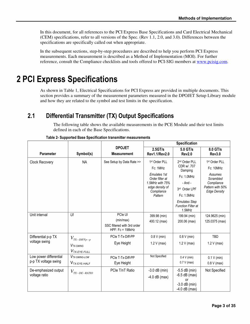
System Board Eye Diagrams
The amplitude and jitter masks are derived from the amplitude and jitter specifications in Table 5.
Figure 4: System Board Compliance Eye Masks

Methods of Implementation
Page 9 of 35
2.5 PCI ExpressModule™ Specifications
The specifications in this section are taken from the PCI Express ExpressModule™ specification,
which is a companion specification to the PCI Express Base specification. Its primary focus is the
implementation of a modular I/O form factor that is focused on the needs of workstations and
servers. Measurements in the PCE module support add-in card and system transmitter path
measurements at the PCI Express connector.
ExpressModule Add-In Card Transmitter Path Specifications
Table 6 is derived from Section 5.4.1 of the ExpressModule Electro-Mechanical Specifications Rev.
1.0.
Table 6 – Supported ExpressModule Add-In Card Measurements
Parameter Symbol DPOJET
Measurement
Rev1.0
Clock Recovery NA See Setup by Data Rate >>
1st Order PLL
Fc: 1MHz
Emulates 1st Order filter at 1.5MHz with 75% edge density of Compliance Pattern
Unit interval UI PCIe UI
(min/max)
SSC filtered with 3rd order HPF: Fc = 198kHz
399.98 (min)
400.12 (max)
Eye height of transition Bits VTXA . Eye Height1 .514 V (min)
1.2 V (max)
Eye height of non-transition Bits VTXA_d Eye Height2 .360 V (min)
Eye width with sample size of 106 UI TTXA
In Rev1.1
Eye Width 287 ps (min)
Jitter eye opening at BER 10-12 Eye Width@BER
274 ps (min)
Informative
Maximum median-max jitter outlier with sample size of 106 UI
JTXA-MEDIAN-to-
MAX-JITTER PCIe Med-Mx
Jitter 56.5 ps (max)

Methods of Implementation
DPOJET PCI Express MOI Page 10 of 35
ExpressModule Add-In Card Eye Diagrams
The amplitude and jitter masks are derived from the amplitude and jitter specifications in Table 6.
Figure 5: ExpressModule add-in card compliance eye masks

Methods of Implementation
Page 11 of 35
ExpressModule System Board Transmitter Path Specifications
Table 7 is derived from Section 5.4.3 of the ExpressModule Electro-Mechanical Specifications Rev.
1.0.
Table 7 – Supported ExpressModule system board measurements
Parameter Symbol DPOJET
Measurement
Gen1
Rev1.0
Clock Recovery NA See Setup by Data Rate >>
2nd Order PLL CDR w/ .707 Damping Fc: 1.0MHz
- And - 1st Order LPF Fc: 1.5MHz
Emulates 3rd Order 3500:250 Method
Unit interval UI PCIe UI
(min/max)
SSC filtered with 3rd order HPF: Fc =
198kHz
399.98 (min)
400.12 (max)
Eye height of transition bits VTXS . Eye Height1 .274 V (min)
1.2 V (max)
Eye height of non-transition bits VTXS_d Eye Height2 .253 V (min)
Eye width with sample size of 106 UI
TTXS Eye Width 246 ps (min)
Jitter eye opening at BER 10-12 Eye Width@BER 233 ps (min)
Maximum median-max jitter outlier with sample size of 106 UI
JTXA-MEDIAN-
to-MAX-JITTER
TIE Jitter 77 ps (max)
Express Module System Board Compliance Eye Diagrams
The amplitude and jitter masks are derived from the amplitude and jitter specifications in Table6.
Figure 6: ExpressModule system board compliance eye masks

Methods of Implementation
DPOJET PCI Express MOI Page 12 of 35
2.6 PCI Express External Cabling Specifications
The specifications in this section are taken from the PCI Express External Cabling Specification. Its
primary focus is the implementation of a cabled interconnect. Measurements in the PCE module
support transmitter path and receiver path measurements. These measurements represent the test
points at the transmitter end of the cable and the receiver end of the cable respectively.
External Cabling Transmitter Path Specifications
Table 8 is derived from Section 3.3.1 of the External Cabling Specification Rev. 1.0.
Table 8 – Supported external cabling transmitter path measurements
Parameter Symbol DPOJET
Measurement
Rev1.0
Clock Recovery NA See Setup by Data Rate >>
1st Order PLL
Fc: 1MHz
Emulates 1st Order filter at 1.5MHz with 75% edge density of Compliance
Pattern
Unit interval UI PCIe UI
(min/max)
SSC filtered with 3rd order HPF: Fc =
198kHz
399.98 (min)
400.12 (max)
Eye height of transition bits VTXA . Eye Height1 .654 V (min)
1.2 V (max)
Eye height of non-transition bits VTXA_d Eye Height2 .450 V (min)
Jitter eye opening at BER 10-12 TrxA @ BER 10-12
Eye Width@BER 296 ps (min)
Eye width with sample size of 106 UI TrxA @ 106
Samples Eye Width 309 ps (min)
Cable (Transmitter Side) Eye Diagrams
The amplitude and jitter masks are derived from the amplitude and jitter specifications.
Figure 7: Cable (transmitter side) compliance eye masks

Methods of Implementation
Page 13 of 35
External Cabling Receiver Path Specifications
Table 9 is derived from Section 3.3.2 of the External Cabling Specification Rev. 1.0.
Table 9 – Supported CEM system board measurements
Parameter Symbol DPOJET
Measurement
Gen1
Rev1.0
Clock Recovery NA See Setup by Data Rate >>
1st Order PLL
Fc: 1MHz
Emulates 1st Order filter at 1.5MHz with 75% edge density of Compliance
Pattern
Unit interval UI PCIe UI
(min/max)
SSC filtered with 3rd order HPF: Fc =
198kHz
399.98 (min)
400.12 (max)
Eye height of transition bits VRXA . Eye Height1 .208 V (min)
1.2 V (max)
Eye height of non-transition bits VRXA_d Eye Height2 .192 V (min)
Jitter eye opening at BER 10-12 TrxA @ BER 10-12
Eye Width@BER 234 ps (min)
Eye width with sample size of 106 UI TrxA @ 106
Samples Eye Width 247 ps (min)
Cable (Receive Side) Eye Diagrams
The amplitude and jitter masks are derived from the amplitude and jitter specifications.
Figure 8: Cable (receiver side) compliance eye masks
Methods of Implementation
DPOJET PCI Express MOI Page 14 of 35
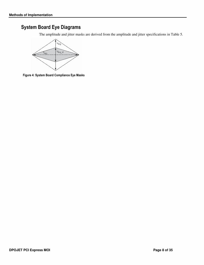
2.7 PCMCIA ExpressCardTM Specifications
The specifications in this section are taken from the PCMCIA ExpressCard Standard (Release 1.0).
Its primary focus is a small modular add-in card technology based on PCI Express and USB
interfaces. Measurements in the PCE module support host system and ExpressCard transmitter path
measurements.
ExpressCard - Module Transmitter Path Specifications
Table 10 is derived from Section 4.2.1.3.2 of the ExpressCard Specification Release 1.0.
Table 10 – Supported ExpressCard transmitter path measurements
Parameter Symbol DPOJET
Measurement
Release 1.0
Clock Recovery NA See Setup by Data Rate >>
1st Order PLL
Fc: 1MHz
Emulates 1st Order filter at 1.5MHz with 75% edge density of Compliance Pattern
Unit interval UI PCIe UI
(min/max)
SSC filtered with 3rd order HPF: Fc =
198kHz
399.98 (min)
400.12 (max)
Eye height of transition bits VTXA . Eye Height1 538 V (min)
1.2 V (max)
Eye height of non-transition bits VTXA_d Eye Height2 .368 V (min)
Eye width across any 250 UIs TTXA Eye Width@BER 237 ps (min)
ExpressCard Transmitter Path Eye Diagrams
The amplitude and jitter masks are derived from the amplitude and jitter specifications in Table 10.
Figure 9: ExpressCard Module Transmitter compliance eye masks
Methods of Implementation
Page 15 of 35
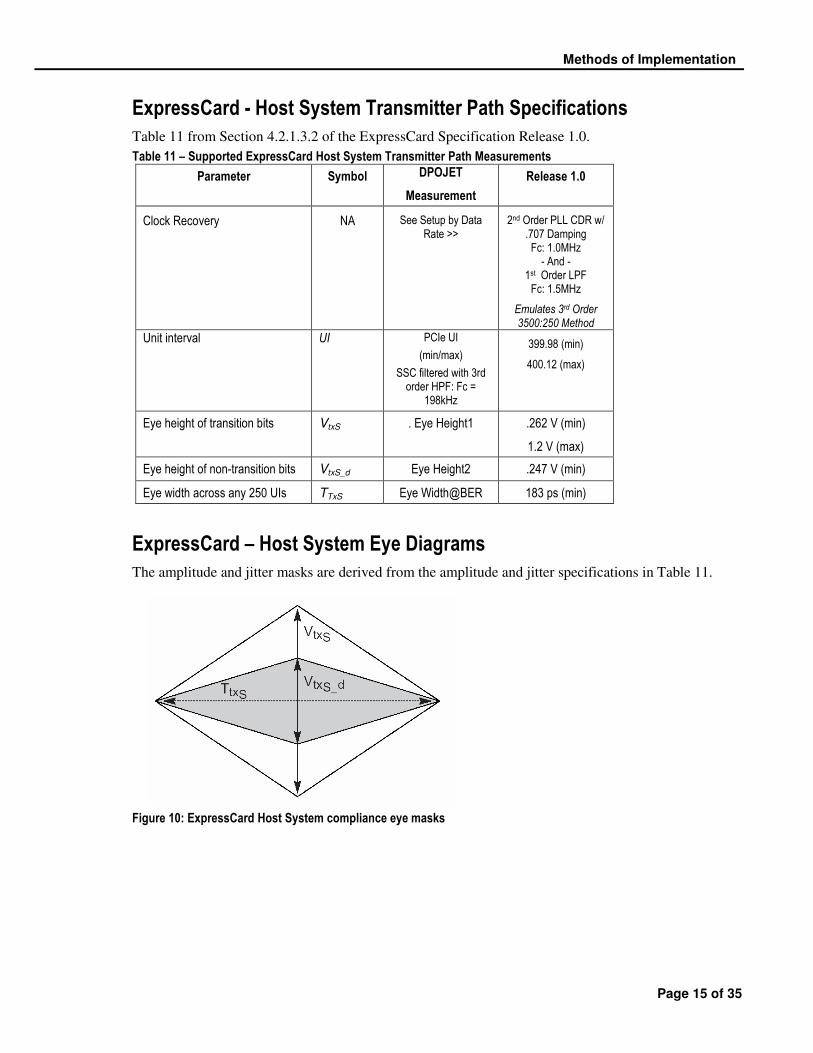
ExpressCard - Host System Transmitter Path Specifications
Table 11 from Section 4.2.1.3.2 of the ExpressCard Specification Release 1.0.
Table 11 – Supported ExpressCard Host System Transmitter Path Measurements
Parameter Symbol DPOJET
Measurement
Release 1.0
Clock Recovery NA See Setup by Data Rate >>
2nd Order PLL CDR w/ .707 Damping Fc: 1.0MHz
- And - 1st Order LPF Fc: 1.5MHz
Emulates 3rd Order 3500:250 Method
Unit interval UI PCIe UI
(min/max)
SSC filtered with 3rd order HPF: Fc =
198kHz
399.98 (min)
400.12 (max)
Eye height of transition bits VtxS . Eye Height1 .262 V (min)
1.2 V (max)
Eye height of non-transition bits VtxS_d Eye Height2 .247 V (min)
Eye width across any 250 UIs TTxS Eye Width@BER 183 ps (min)
ExpressCard – Host System Eye Diagrams
The amplitude and jitter masks are derived from the amplitude and jitter specifications in Table 11.
Figure 10: ExpressCard Host System compliance eye masks

Methods of Implementation
DPOJET PCI Express MOI Page 16 of 35
3 PCI Express Library Contents The following table shows a list of the PCI Express standards supported by the DPOJET Setup Library and their default
probing configurations. The Setup File Library is located in C:\TekApplications\DPOJET\PCIE\Setups
Table 12 – Setup Files and default probing configurations
PCI-SIG Specification Bit Rate Setup File Name Default Probing
Configuration
Rev1.1 Base Specification
Transmitter and Receiver
2.5GT/s Rev11_Tx_Base.set
Rev11_Rx_Base.set
Data = Math1 – Ch1-Ch2
Rev1.1 CEM Specification
Add-In Card and System
2.5GT/s Rev11_Tx_ADD_CON.set
Rev11_Tx_SYSTEM.set
Data = Math1 – Ch1-Ch2
Rev1.0 Cable
Specification
Near End and Far End
2.5GT/s Rev10_Tx_Cable.set
Rev10_Rx_Cable.set
Data = Math1 – Ch1-Ch2
Rev1.0 ExpressModule
Specification
Add-In Card and System
2.5GT/s Rev10_Tx_ExpMod_ADD_CON.set
Rev10_Tx_ExpMod_SYSTEM.set
Data = Math1 – Ch1-Ch2
Rev1.0 ExpressCard
Specification
Host and Module
2.5GT/s Rev10_Tx_ExpressCard_Host.set
Rev10_Tx_ExpressCard_Module.set
Data = Math1 – Ch1-Ch2
Rev2.0 Base Specification
Transmitter with 3.5dB
and 6.0 dB De-Emphasis
and Low Swing
5GT/s Rev20_Base_Tx_3.5dB.set
Rev20_Base_Tx_6.0dB.set
Rev20_Base_Tx_Low_Swing.set
Data = Math1 – Ch1-Ch2
Rev2.0 CEM Specification
Add-In Card with 3.5dB
and 6.0dB De-Emphasis
and System
5GT/s Rev20_Tx_ADD_CON_3.5dB.set
Rev20_Tx_ADD_CON_6.0dB.set
Rev20_Tx_SYSTEM.set
Add-In Card:
Data = Math1 – Ch1-Ch2
System:
RefClk = Math1 = Ch1-Ch2
Data = Math2 = Ch3 – Ch4
Rev 3.0 Base Specification
(Draft)
Transmitter Full and Half
Swing
8GT/s Rev30_Base_Tx.set
Rev30_Base_Tx_Half_Swing.set
Data = Math1 – Ch1-Ch2
To change the probing configuration to use differential probes, change the Source of the Data and
RefClk as appropriate in the measurement configuration menu in DPOJET. Refer to the DPOJET
OLH (Online Help) for details.

Methods of Implementation
Page 17 of 35
4 Preparing to Take Measurements 4.1 Required Equipment
The following equipment is required to take the measurements:
• Oscilloscope Selection:
o Rev 1.1 (2.5 GT/s) – The PCI-SIG recommends a minimum of 6 GHz system BW for
compliance testing. However, some silicon can have rise times in the 50ps range. Thus,
Tektronix recommends DPO/DSA70000 8GHz and above for 2.5GT/s transmitter
measurements.
o Rev 2.0 (5 GT/s) – DPO/DSA70000 12.5 GHz and above are recommended for 5GT/s
and above and required for Base Specification transmitter measurements.
o Rev 3.0 (8 GT/s) – DPO/DSA70000 16 GHz and above are recommended for 8GT/s
measurements.
• DPOJET software (Version 2.1 or above) with PCI Express Measurements (Opt. PCE) installed.
• Probes – See Section 3.2 for probing options.
• Test Fixtures
o Test Fixtures for System and Add-In card testing are available from the PCI-SIG. Rev1.1
Fixtures (CLB1, CBB1) break transmitter signals out into SMA connections. Rev 2.0
Fixtures (CLB2, CBB2) break transmitter signals out into SMP connections. These
fixtures are available at:
http://www.pcisig.com/specifications/ordering_information/ordering_information.
o Test fixtures for ExpressCard testing are available from the following URL:
http://www.expresscard.org/web/site/testtools.jsp
Methods of Implementation
DPOJET PCI Express MOI Page 18 of 35
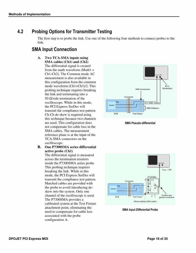
4.2 Probing Options for Transmitter Testing
The first step is to probe the link. Use one of the following four methods to connect probes to the
link.
SMA Input Connection
A. Two TCA-SMA inputs using
SMA cables (Ch1) and (Ch2) The differential signal is created
from the math waveform (Math1 =
Ch1-Ch2). The Common mode AC
measurement is also available in
this configuration from the common
mode waveform (Ch1+Ch3)/2. This
probing technique requires breaking
the link and terminating into a
50 Ω/side termination of the
oscilloscope. While in this mode,
the PCI Express SerDes will
transmit the compliance test pattern.
Ch-Ch de-skew is required using
this technique because two channels
are used. This configuration does
not compensate for cable loss in the
SMA cables. The measurement
reference plane is at the input of the
TCA-SMA connectors on the
oscilloscope.
SMA Pseudo-differential
B. One P7300SMA series differential
active probe (Ch1) The differential signal is measured
across the termination resistors
inside the P7300SMA series probe.
This probing technique requires
breaking the link. While in this
mode, the PCI Express SerDes will
transmit the compliance test pattern.
Matched cables are provided with
the probe to avoid introducing de-
skew into the system. Only one
channel of the oscilloscope is used.
The P7300SMA provides a
calibrated system at the Test Fixture
attachment point, eliminating the
need to compensate for cable loss
associated with the probe
configuration A.
SMA Input Differential Probe

Methods of Implementation
Page 19 of 35
ECB pad connection
C. Two active probes (Ch1) and
(Ch2) The differential signal is created
from the math waveform
(Math1 = Ch1-Ch2). The
Common mode AC/DC
measurements are available in
this configuration from the
common mode waveform
(Ch1+Ch3)/2. This probing
technique can be used for either
a live link that is transmitting
data, or a link that has
terminated into a “dummy
load.” In both cases, the single-
ended signals should be probed
as close as possible to the
termination resistors on both
sides with the shortest ground
connection possible. Ch-Ch de-
skew is required using this
technique because two channels
are used.
D. One P7300 or P7500 series
Differential probe (Ch1) The differential signal is
measured directly across the
termination resistors. This
probing technique can be used
for either a live link that is
transmitting data, or a link that
is terminated into a “dummy
load.” In both cases, the signals
should be probed as close as
possible to the termination
resistors. De-skew is not
necessary because a single
channel of the oscilloscope is
used. If using a P7500 Tri-
Mode Probe, common mode
voltage measurements can be
made directly with the probe.

Methods of Implementation
DPOJET PCI Express MOI Page 20 of 35
Dual Port Connection E. Dual Port
For Rev 2.0 System testing
(Described in Section 2.4), the
‘Dual Port’ method is used to
capture differential Data and
RefClk. Direct SMA input can
be used (where
RefClk=Math1=Ch1-Ch2 and
Data=Math2=Ch3-Ch4); or
Two P7313SMA probes can be
used (where RefClk = Ch1 and
Data = Ch2).
Methods of Implementation
Page 21 of 35
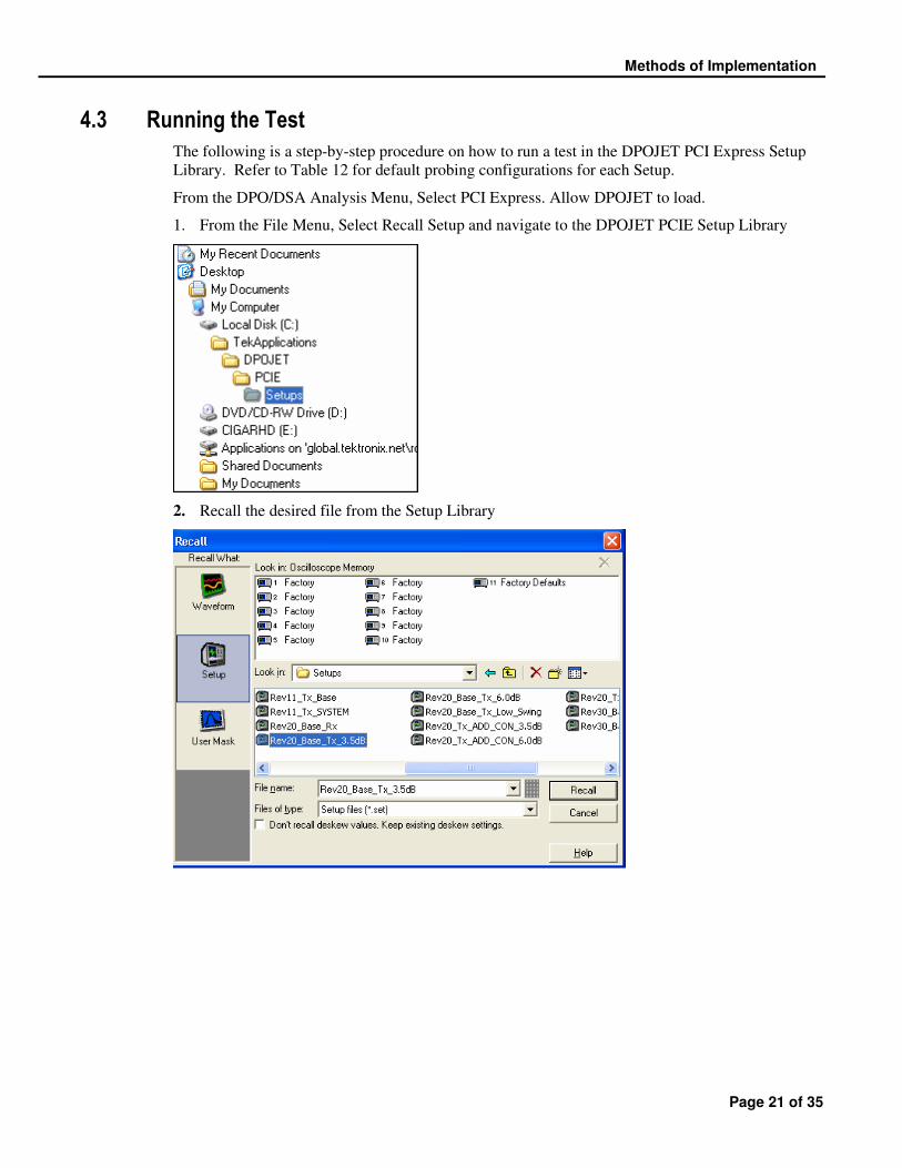
4.3 Running the Test
The following is a step-by-step procedure on how to run a test in the DPOJET PCI Express Setup
Library. Refer to Table 12 for default probing configurations for each Setup.
From the DPO/DSA Analysis Menu, Select PCI Express. Allow DPOJET to load.
1. From the File Menu, Select Recall Setup and navigate to the DPOJET PCIE Setup Library
2. Recall the desired file from the Setup Library
Methods of Implementation
DPOJET PCI Express MOI Page 22 of 35
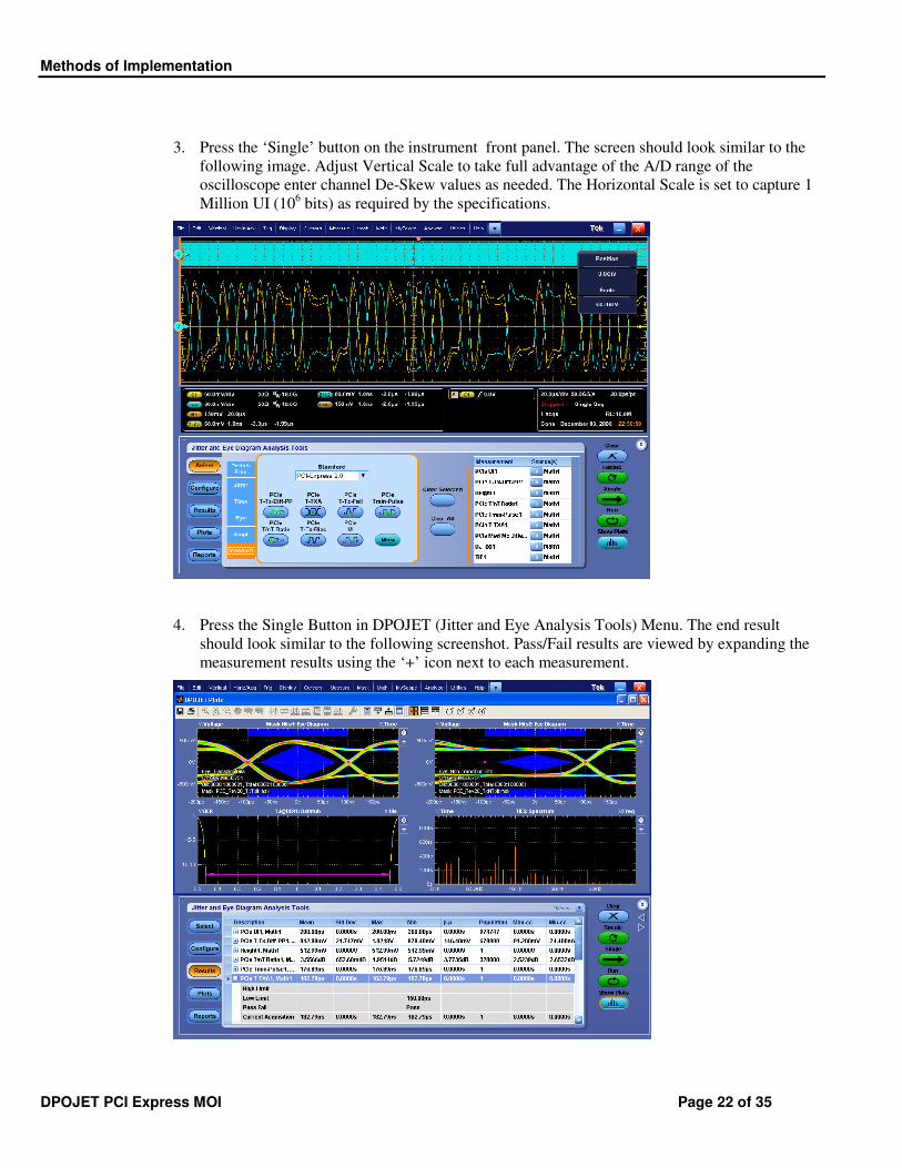
3. Press the ‘Single’ button on the instrument front panel. The screen should look similar to the
following image. Adjust Vertical Scale to take full advantage of the A/D range of the
oscilloscope enter channel De-Skew values as needed. The Horizontal Scale is set to capture 1
Million UI (106 bits) as required by the specifications.
4. Press the Single Button in DPOJET (Jitter and Eye Analysis Tools) Menu. The end result
should look similar to the following screenshot. Pass/Fail results are viewed by expanding the
measurement results using the ‘+’ icon next to each measurement.
Methods of Implementation
Page 23 of 35
5 Parameter Definitions and Method of implementation The DPOJET PCI Express Setup Library combines measurements native to the standard DPOJET package with
with unique measurements offered in the Standards >> PCI Express 2.0 tab of the DPOJET Measurement
Select menu. PCI Express specific measurements require Opt. PCE is enabled and Version 2.1 or above of
DPOJET is installed on the oscilloscope.
Measurements selected in the setup file are dependent on the specification that is designed to test. Refer to
Table 2 thru Table 11 for the clock recovery method and measurements for each measurement in the setup file.
Refer to the DPOJET OLH (Online Help) for measurement algorithms and setup parameters for measurements
native to DPOJET.
The algorithm and setup parameters of the PCI Express specific measurements are described in the following
sections.
5.1 UI (Unit Interval) MOI
Definition:
UI (Unit Interval) is defined in the base specification Rev2.0. This measurement is done using the
PCIe–UI. The Result panel would display the Unit interval values
Test Definition Notes from the Specification:
The specified UI is equivalent to a tolerance of ±300 ppm for each Refclk source. Period does not
account for SSC induced variations.
Limits:
Refer to Table 2 thru Table 11 for specified limits on the UI measurement.
Test Procedure:
Ensure that PCIe UI is selected in the Jitter and Eye diagram Analysis Tools >> Select menu.
Set the following parameters
Horizontal Record length to at least 500K.
Configure >> Edges >> Auto
Configure >> Filter >> Low pass - 198kHz
Configure >> Global >> off
Measurement Algorithm:
The Unit interval measurement calculates the duration of a cycle as defined by a start and a stop edge. Edges are defined by polarity, threshold, and hysteresis. The application calculates clock period measurement using the following equation:

Methods of Implementation
DPOJET PCI Express MOI Page 24 of 35
Where:
PClock
is the clock period.
T is the VRefMid crossing time for the selected polarity.
5.2 TX Differential Pk-Pk Output Voltage MOI
Definition:
pDIFFpTXV−− (Differential Output Pk-Pk Voltage) is defined in the base specification Rev 2.0. This
measurement is done using PCIe T-Tx-Diff-PP. The Result panel would display the Mean , Maximum
and Minimum differential output pk-pk voltage.
Test Definition Notes from the Specification:
||2−−+−−−
−∗= DTXDTXpDIFFpTX VVV
Measured on individual bits, first bit from a sequence in which all bits have same polarity, over
specified number of UIs. The voltage measurement is referenced to the centre of each UI.
Limits:
Refer to Table 2 thru Table 11 for specified limits on the pDIFFpTXV−− measurement
Test Procedure:
Ensure that PCIe T-Tx-Diff-PP is selected in the Jitter and Eye diagram Analysis Tools >> Select
menu.
Select Configure >> Clock Recovery. Configure the Clock Recovery to be consistent with the Clock
Recovery method shown in Tables 2-11.
Measurement Algorithm:
Differential Peak Voltage Measurement: The Differential Peak Voltage measurement returns two times
the larger of the Min or Max statistic of the differential voltage waveform.
)))(());(((2 ivMinivMaxMaxV DIFFDIFFPKDIFF ∗=−
Where:
i is the index of all waveform values
DIFFv is the differential voltage signal
Methods of Implementation
Page 25 of 35
5.3 TX De-Emphasis Ratio
Definition:
VTX-DE-RATIO(De-Emphasized Differential Output Voltage (Ratio)) is defined in the base specification.
This measurement uses PCIe T/nT ratio measurement.
Test Definition Notes from the Specification:
This is the ratio of the VTX-DIFFp-p of the second and the following bits after a transition divided by the
VTX-DIFFp-p of the first bit after a transition.
Limits:
Refer to Table 2 thru Table 11 for specified limits on the pDIFFpTXV−− measurement
Measurement Algorithm:
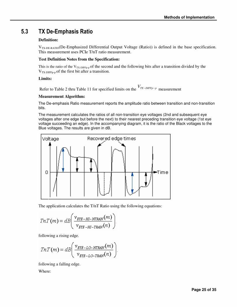
The De-emphasis Ratio measurement reports the amplitude ratio between transition and non-transition bits.
The measurement calculates the ratios of all non-transition eye voltages (2nd and subsequent eye voltages after one edge but before the next) to their nearest preceding transition eye voltage (1st eye voltage succeeding an edge). In the accompanying diagram, it is the ratio of the Black voltages to the Blue voltages. The results are given in dB.
The application calculates the T/nT Ratio using the following equations:
following a rising edge.
following a falling edge.
Where:
Methods of Implementation
DPOJET PCI Express MOI Page 26 of 35
vEYE–HI–TRAN is the High voltage at the interpolated midpoint of the first unit interval following a positive
transition.
vEYE–LO–TRAN is the Low voltage at the interpolated midpoint of the first unit interval following a negative
transition.
vEYE–HI–NTRAN is the High voltage at the interpolated midpoint of all unit intervals except the first
following a positive transition.
vEYE–LO–NTRAN is the Low voltage at the interpolated midpoint of all unit intervals except the first
following a negative transition.
m is the index for all non-transition UIs.
n is the index for the nearest transition UI preceding the UI specified by m.
In a time trend plot of the measurement results, there is one measurement for each non-transition bit in
the waveform (that is the black arrows in the diagram).
NOTE. PCIe T/nT Ratio measurement uses Brick Wall filter.
5.4 TX Minimum Pulse Width MOI
Definition:
TMIN-PULSE (Instantaneous lone pulse width measurement) is defined in the base specification Rev2.0.
This measurement is done using the PCIe Tmin-Pulse. The Result panel would display the minimum
pulse width results.
Test Definition Notes from the Specification:
TMIN-PULSE (Instantaneous lone pulse width measurement) is measured from transition center to the next
transition center, and that the transition centers will not always occur at the differential zero crossing
point. In particular, transitions from a de-emphasized level to a full level will have a center point offset
from the differential zero crossing.
Limits:
Refer to Table 2 thru Table 11 for specified limits on the TMIN-PULSE measurement
Test Procedure:
Ensure that PCIe Tmin-Pulse is selected in the Jitter and Eye diagram Analysis Tools >> Select
menu.
Set the following parameters
Select Configure >> Clock Recovery. Configure the Clock Recovery to be consistent with the Clock
Recovery method shown in Tables 2-11.
Configure >> General >>Off
Configure >> Global >> Off
Methods of Implementation
Page 27 of 35
Measurement Algorithm:
Tmin-Pulse (minimum single pulse width TMin-Pulse) is measured from one transition center to the next.
The application calculates TMin-Pulse using the following equation:
Where:
TMin-Pulse is the minimum pulse width
T is the transition center
5.5 TX Rise/Fall Time Mismatch MOI
Definition:
TRF-MISMATCH (Rise time, Fall time mismatch) is defined in the base specification. This measurement is
done using PCIe T-RF-Mismch. The Result panel would display the Mean , Maximum and Minimum
Rise time, Fall time mismatch values.
Limits:
Refer to Table 2 thru Table 11 for TRF-MISMATCH measurement.
Test Procedure:
Ensure that PCIe T-RF-Mismch is selected in Jitter and Eye diagram Analysis Tools >> Select
menu is selected.
Set the following parameters
Select Configure >> Clock Recovery. Configure the Clock Recovery to be consistent with the Clock
Recovery method shown in Tables 2-11.
Configure >> Filter >> No filter
Configure >> General >>Off
Configure >> Global >> Population
Measurement Algorithm:
PCIe T-RF-Mismch (Rise and Fall Time mismatch measurement) is the mismatch between Rise time
(TRise) and Fall time(TFall). The application calculates this measurement using the following equation:
Where:

Methods of Implementation
DPOJET PCI Express MOI Page 28 of 35
TMismatch
is the rise and fall time mismatch
TRise
is the rise time
TFall
is the fall time
5.6 Minimum TX Eye Width MOI
Definition:
EYETXT−
(Minimum TX Eye Width) is defined in the base specification. . See Section 4.7.2 of PCI
EXPRESS CARD ELECTROMECHANICAL SPECIFICATION, REV. 2.0 for the Gen2 definition for
both 3.5dB and 6dB De-emphasis. The eye diagrams defined in this section represent the compliance
eye diagrams that must be met for both the add-in card and a system board interfacing with such an
add-in card. A sample size of 106 UI is assumed for the measurement.
EYETXT−
is defined to be the Jitter Eye Opening.
Test Definition Notes from the Specification:
- The maximum Transmitter jitter can be derived as EYETXJITTERTXMAX TT−−
−= 1
- Specified at the measurement point into a timing and voltage compliance test load as shown in the
base specification and measured over the specified number of UIs. Also refer to the transmitter
compliance eye diagram shown in the base specification.
Limits:
Refer to Table 2 thru Table 11 on the EYETXT−
measurement.
Test Procedure:
Ensure that the measurement PCI T-TXA is selected in the Jitter and Eye diagram Analysis Tools >>
Select menu.
Configure the measurement by setting the following parameters.
Select Configure >> Clock Recovery. Configure the Clock Recovery to be consistent with the Clock
Recovery method shown in Tables 2-11.
Configure >> General >> off.
Measurement Algorithm:
The measured minimum horizontal eye opening at the zero reference level as shown in the eye diagram
below.
PkPkAVGWIDTHEYE TIEUIT−−
−=
Where:

Methods of Implementation
Page 29 of 35
AVGUI is the average UI
PkPkTIE−
is the Peak-Peak TIE
Figure 10: Add-in Card Transmitter Path Compliance Eye Diagram
Where TtxA is the Eye width, VtxA is the full scale peak to peak voltage and VtxA_d is the De-emphasized
peak to peak voltage.
Figure 11: Configure Panel
5.7 TX Median-to-Max Jitter MOI
Definition:
MAXJITTERtoEYEMEDIANTXT−−− (maximum time between the jitter median and maximum deviation from the
median.).A step response Band pass filter is being used to remove the low frequency jitter as specified
in Rev2.0 of the base specification .
Limits:
Refer to Table 2 thru Table 11 for MAXJITTERtoEYEMEDIANTXT−−−
measurement.
Test Procedure:
Ensure that PCIe Med-Mx Jitter is selected in Jitter and Eye diagram Analysis Tools >> Select
menu is selected.
Set the following parameters
Configure >> Edges >> Signal Type >> Auto
Methods of Implementation
DPOJET PCI Express MOI Page 30 of 35
Select Configure >> Clock Recovery. Configure the Clock Recovery to be consistent with the Clock
Recovery method shown in Tables 2-11.
Configure >> Filter >> Brick Wall Filter
Configure >> General >>Off
Measurement Algorithm:
The measured time difference between a data edge and a recovered clock edge.
)()()( ntntntie DATDATR −=−
Where:
DATt is the original data edge
DATRt − is the recovered data edge (for example, the recovered clock edge corresponding to the UI
boundary of DATt)
n is the index of all edges in the waveform
Med_Tie= median (tie (n))
Where:
Med_Tie is the Median of the tie measured.
TTx-EYEMEDIAN-to MAXJitter = Abs (Med_Tie – Maximum deviation of tie (n) from the Med_Tie)