DPO2039 - Diodes
13
DPO2039 Document number: DS42776 Rev. 1 - 2 1 of 13 www.diodes.com May 2020 © Diodes Incorporated DPO2039 4-CH OVER-VOLTAGE PROTECTION FOR CC/DIFF PINS ON USB TYPE-C Description The DPO2039 provides 4 channels of over-voltage protection over the CC1/2 & DIFF1/2 pins which are connected to the USB Type-C connector. The 4 channels are divided into two pairs, one pair of channels protect the CC1 and CC2 pins from being shorted to the VBUS, one pair of channels protect the DIFF1 and DIFF2 pins from being shorted to the VBUS. Whenever the voltage threshold set for any of the two pairs of channels is reached, the exception condition becomes valid and the low-active flag FAULTB is subsequently asserted. This device is designed to draw its operating voltage primarily from the system power, VSYS, which is either the always-ON 3.3/5V existed within the system or the 1-cell battery inside the mobile system. Under the circumstance when the battery inside a mobile system is fully depleted, DPO2039 can obtain power from the external peripheral system connected to the USB Type-C connector. The DPO2039 is housed in the low-profile and space-saving U-QFN3030- 16 (Type B) package which is manufactured with environmental- friendly material. Features Operating Voltage Range: 2.7V to 5.5V 4-Channel Over-Voltage Protection with Auto-Recovery IEC 61000-4-2 ESD Protection over CCxC and DIFFxC Pins RDS(ON) of OVP MOSFET for CC-Pin Protection: 300mΩ Typical RDS(ON) of OVP MOSFET for DIFF-Pin Protection: 5Ω Typical CIN of OVP MOSFET for CC-Pin Protection: 50pF CIN of OVP MOSFET for DIFF-Pin Protection: 5pF Built-In Over-Temperature Protection Totally Lead-Free & Fully RoHS Compliant (Notes 1 & 2) Halogen and Antimony Free. “Green” Device (Note 3) For automotive applications requiring specific change control (i.e. parts qualified to AEC-Q100/101/200, PPAP capable, and manufactured in IATF 16949 certified facilities), please contact us or your local Diodes representative. https://www.diodes.com/quality/product-definitions/ Pin Assignments (Top View) 1 3 4 DIFF1C DIFF2C CC1C CC2C 7 VSYS 6 NC 11 12 10 9 14 15 DIFF1S DIFF2S CC1S CC2S GND 5 8 NC CB 16 13 NC NC FAULTB 2 U-QFN3030-16 (Type B) Applications Notebook/Desktop/AIO PCs, Tablets, Mobile Phones VR/AR Headsets Docking Stations, Universal & Multimedia Hubs FPTVs, PC Monitors Set-Top-Boxes, Residential Gateways, Storage Devices Universal AC/DC Chargers/Adapters Notes: 1. No purposely added lead. Fully EU Directive 2002/95/EC (RoHS), 2011/65/EU (RoHS 2) & 2015/863/EU (RoHS 3) compliant. 2. See https://www.diodes.com/quality/lead-free/ for more information about Diodes Incorporated’s definitions of Halogen- and Antimony-free, "Green" and Lead-free. 3. Halogen- and Antimony-free "Green” products are defined as those which contain <900ppm bromine, <900ppm chlorine (<1500ppm total Br + Cl) and <1000ppm antimony compounds.
Transcript of DPO2039 - Diodes

DPO2039 Document number: DS42776 Rev. 1 - 2
1 of 13 www.diodes.com
May 2020 © Diodes Incorporated
DPO2039
4-CH OVER-VOLTAGE PROTECTION FOR CC/DIFF PINS ON USB TYPE-C
Description
The DPO2039 provides 4 channels of over-voltage protection over
the CC1/2 & DIFF1/2 pins which are connected to the USB Type-C
connector. The 4 channels are divided into two pairs, one pair of
channels protect the CC1 and CC2 pins from being shorted to the
VBUS, one pair of channels protect the DIFF1 and DIFF2 pins from
being shorted to the VBUS. Whenever the voltage threshold set for any
of the two pairs of channels is reached, the exception condition
becomes valid and the low-active flag FAULTB is subsequently
asserted.
This device is designed to draw its operating voltage primarily from
the system power, VSYS, which is either the always-ON 3.3/5V existed
within the system or the 1-cell battery inside the mobile system.
Under the circumstance when the battery inside a mobile system is
fully depleted, DPO2039 can obtain power from the external
peripheral system connected to the USB Type-C connector. The
DPO2039 is housed in the low-profile and space-saving U-QFN3030-
16 (Type B) package which is manufactured with environmental-
friendly material.
Features
Operating Voltage Range: 2.7V to 5.5V
4-Channel Over-Voltage Protection with Auto-Recovery
IEC 61000-4-2 ESD Protection over CCxC and DIFFxC Pins
RDS(ON) of OVP MOSFET for CC-Pin Protection: 300mΩ Typical
RDS(ON) of OVP MOSFET for DIFF-Pin Protection: 5Ω Typical
CIN of OVP MOSFET for CC-Pin Protection: 50pF
CIN of OVP MOSFET for DIFF-Pin Protection: 5pF
Built-In Over-Temperature Protection
Totally Lead-Free & Fully RoHS Compliant (Notes 1 & 2)
Halogen and Antimony Free. “Green” Device (Note 3)
For automotive applications requiring specific change
control (i.e. parts qualified to AEC-Q100/101/200, PPAP
capable, and manufactured in IATF 16949 certified facilities),
please contact us or your local Diodes representative.
https://www.diodes.com/quality/product-definitions/
Pin Assignments
(Top View)
1
3
4
DIFF1C
DIFF2C
CC1C
CC2C
7
VSY
S6
NC
11
12
10
9
1415
DIFF1S
DIFF2S
CC1S
CC2S
GN
D
5 8
NC CB
16
13
NC
NC
FAU
LTB
2
U-QFN3030-16 (Type B)
Applications
Notebook/Desktop/AIO PCs, Tablets, Mobile Phones
VR/AR Headsets
Docking Stations, Universal & Multimedia Hubs
FPTVs, PC Monitors
Set-Top-Boxes, Residential Gateways, Storage Devices
Universal AC/DC Chargers/Adapters
Notes: 1. No purposely added lead. Fully EU Directive 2002/95/EC (RoHS), 2011/65/EU (RoHS 2) & 2015/863/EU (RoHS 3) compliant. 2. See https://www.diodes.com/quality/lead-free/ for more information about Diodes Incorporated’s definitions of Halogen- and Antimony-free, "Green" and
Lead-free. 3. Halogen- and Antimony-free "Green” products are defined as those which contain <900ppm bromine, <900ppm chlorine (<1500ppm total Br + Cl) and <1000ppm antimony compounds.

DPO2039 Document number: DS42776 Rev. 1 - 2
2 of 13 www.diodes.com
May 2020 © Diodes Incorporated
DPO2039
Typical Application Circuit
DPO2039DABQ
VSYS
DIFF1C
CC1C
CC2C
FAULTB
12
11
10
9
GND
CC1S
DIFF2S
DIFF1S
RFAULTB
10kΩ
VCC
DIFF2C
CSYS
1uF
CC2S
VDIFF1S
VDIFF2S
VCC1S
VCC2S
VDIFF1C
VDIFF2C
VCC1C
VCC2C
DIFF1
US
B T
ype-C
Recepta
cle
DIFF2
CC1
CC2
CC1
CC2USB PD controller
DIFF1
DIFF2 To system
6
VCC
8
14
1
2
3
4
15
NC NC
5 x xCB
7
Figure 1. Typical Application Circuit
Pin Descriptions
Pin Number Pin Name Function
1 DIFF1C DIFF1 connector side. This shall be connected to the DIFF1 pin of the USB Type-C connector.
2 DIFF2C DIFF2 connector side. This shall be connected to the DIFF2 pin of the USB Type-C connector.
3 CC1C CC1 connector side. This shall be connected to the CC1 pin of the USB Type-C connector.
4 CC2C CC2 connector side. This shall be connected to the CC2 pin of the USB Type-C connector.
7 CB Pin for ESD support capacitor. Place a 0.1μF capacitor on this pin to ground.
8 FAULTB Fault status. This is an active-low open-drain output.
9 CC2S CC2 system side. This shall be connected to the CC2 pin of the component to be protected.
10 CC1S CC1 system side. This shall be connected to the CC1 pin of the component to be protected.
11 DIFF2S DIFF2 system side. This shall be connected to the DIFF2 pin of the component to be protected.
12 DIFF1S DIFF1 system side. This shall be connected to the DIFF1 pin of the component to be protected.
5, 6, 13, 16 NC No connection.
14 GND Ground.
15 VSYS Power Input. This shall be connected to the 2.7 to 5.5V power source inside the system.
— EP Exposed pad. This shall be connected to ground.
1μF
DPO2039

DPO2039 Document number: DS42776 Rev. 1 - 2
3 of 13 www.diodes.com
May 2020 © Diodes Incorporated
DPO2039
Functional Block Diagram
Figure 2. Internal Functional Blocks
Absolute Maximum Ratings (@ TA = +25°C, unless otherwise specified) (Note 4)
Symbol Parameter Rating Unit
VVSYS Voltage Range of VSYS Pin -0.3 to 6.0 V
VFAULTB Voltage Range of FAULTB Pin -0.3 to 6.0 V
VCB Voltage Range of CB Pin -0.3 to 24 V
VDIFFxS, VCCxS Voltage Range of DIFF1S, DIFF2S, CC1S, CC2S Pins -0.3 to 6.0 V
VDIFFxC, VCCxC Voltage Range of DIFF1C, DIFF2C, CC1C, CC2C Pins -0.3 to 24.0 V
TJ Operating Junction Temperature -40 to +150 °C
TL Lead Temperature +260 °C
TSTG Storage Temperature -65 to +150 °C
ESD Human Body Model (HBM), JESD22-A114 ±2.0
kV Charge Device Model (CDM), JESD22-C101 ±0.5
Note: 4. These are stress ratings only. Operation outside the absolute maximum ratings can cause device failure.
Operation at the absolute maximum rating for extended periods can reduce device reliability.
Package Thermal Data (@ TA = +25°C, unless otherwise specified) (Note 5)
Symbol Parameter Rating Unit
PD Power Dissipation 1.75 W
RθJA Thermal Resistance, Junction-to-Ambient 73 °C/W
RθJC Thermal Resistance, Junction-to-Case 12.7 °C/W
Note: 5. Device mounted on FR-4 substrate PC board, 2oz copper, with 1” 1” copper pad layout.
DPO2039 Document number: DS42776 Rev. 1 - 2
4 of 13 www.diodes.com
May 2020 © Diodes Incorporated
DPO2039
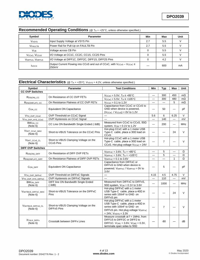
Recommended Operating Conditions (@ TA = +25°C, unless otherwise specified.)
Symbol Parameter Min Max Unit
VVSYS Input Supply Voltage at VSYS Pin 2.7 5.5 V
VFAULTB Power Rail for Pull-Up on FAULTB Pin 2.7 5.5 V
VCB Voltage across CB Pin 0 5.5 V
VCCxC, VCCxS I/O Voltage at CC1C, CC2C, CC1S, CC2S Pins 0 5.5 V
VDIFFxC, VDIFFxS I/O Voltage at DIFF1C, DIFF2C, DIFF1S, DIFF2S Pins 0 4.2 V
IVCCX Output Current Flowing into CCxS and out of CCxC, with VCCxS – VCCxC ≤ 250mV
— 600 mA
Electrical Characteristics (@ TA = +25°C, VVSYS = 4.2V, unless otherwise specified.)
Symbol Parameter Test Conditions Min Typ Max Unit
CC OVP Switches
RDS(ON)_CC On Resistance of CC OVP FETs VCCxC = 5.5V, TA ≤ +85°C — 300 450 mΩ
VCCxC = 5.5V, TA ≤ +105°C — 300 480 mΩ
RDS(ONFLAT)_CC On Resistance Flatness of CC OVP FETs VCCxC = 0.1 to 1.2V — — 5 mΩ
CON_CC Equivalent ON Capacitance
Capacitance from CCxC or CCxS to GND when device is powered,
(VCCxC / VCCxS) = 0V to 1.2V
— 50 — pF
VTH_OVP_CCxC OVP Threshold on CCxC Signal — 5.6 6 6.25 V
VTH_OVP_HYS_CCxC OVP Hysteresis on CCxC Signal — — 140 — mV
BWON_CC
(Note 6) CC Line ON Bandwidth Single Ended (-3dB)
Measured from CCxC to CCxS, 50Ω
system, VCM = 0.1V to 1.2V — 200 — MHz
VSHT_CCxC_MAX
(Note 6) Short-to-VBUS Tolerance on the CCxC Pins
Hot-plug CCxC with a 1 meter USB Type-C cable, place a 30Ω load on CCxS
— — 24 V
VSHT_CCxS_CL
(Note 6)
Short-to-VBUS Clamping Voltage on the CCxS Pins
Hot-plug CCxC with a 1 meter USB Type-C cable, place a 30Ω load on
CCxS. Hot plug voltage VCCxC = 24V
— 7 — V
DIFF OVP Switches
RDS(ON)_DIFF On Resistance of DIFF OVP FETs VDIFFxC = 3.6V, TA = +85°C — 5 — Ω
VDIFFxC = 3.6V, TA = +105°C — 5 — Ω
RDS(ONFLAT)_DIFF On Resistance Flatness of DIFF OVP FETs VDIFFxC = 0.1 to 3.6V — — 1 Ω
CON_DIFF Equivalent ON Capacitance
Capacitance from DIFFxC or DIFFxS to GND when device is
powered. VDIFFxC / VDIFFxS = 0V to 3.6V
— 5 — pF
VTH_OVP_DIFFxC OVP Threshold on DIFFxC Signals — 4.15 4.5 4.75 V
VTH_OVP_HYS_DIFFxC OVP Hysteresis on DIFFxC Signals — — 110 — mV
BWON_DIFF
(Note 6)
DIFF line ON Bandwidth Single Ended (-3dB)
Measured from DIFFxC to DIFFxS,
50Ω system, VCM = 0.1V to 3.6V — 1000 — MHz
VSHTBUS_DIFFxC_MAX
(Note 6)
Short-to-VBUS Tolerance on the DIFFxC Pins
Hot-plug DIFFxC with a 1 meter USB Type-C cable, place a 40Ω in series with 150nF to GND on DIFFxS pin
— — 24 V
VSHTBUS_DIFFxS_CL
(Note 6)
Short-to-VBUS Clamping Voltage on the DIFFxS Pins
Hot-plug DIFFxC with a 1 meter USB Type-C cable, place a 40Ω in series with 100nF to GND on
DIFFxS pin. Hot plug voltage VDIFFxC
= 24V, VVSYS = 3.3V
— 7 — V
XTALK_DIFFx
(Note 6) Crosstalk between DIFFx Lines
Measure crosstalk at f = 1MHz, from DIFF1S to DIFF2C or DIFF2 to
DIFF1C. VCM1 = 3.6V, VCM2 = 0.3V, terminate open sides to 50Ω
— -80 — dB

DPO2039 Document number: DS42776 Rev. 1 - 2
5 of 13 www.diodes.com
May 2020 © Diodes Incorporated
DPO2039
Electrical Characteristics(@ TA = +25°C, VVSYS = 4.2V, unless otherwise specified) (continued)
Symbol Parameter Test Conditions Min Typ Max Unit
Power Supply and Leakage Current
VUVLO VVSYS under Voltage Lockout VVSYS steps up from 2V until CC or DIFF FETs turn ON
2.15 2.4 2.55 V
VUVLO_HSYS VVSYS UVLO Hysteresis
VVSYS steps down from 2.5V until CC or DIFF FETs turn off. Measure difference between rising and falling UVLO to calculate
— 200 — mV
IVSYS_ON VVSYS Supply Current — — 190 — μA
ILEAK_CCxC Leakage current for CCxC when device is powered
VCCxC = 3.6V — — 30 μA
ILEAK_DIFFxC Leakage current for DIFFxC when device is powered
VDIFFxC = 3.6V — — 35 μA
ILEAK_CCxS Leakage current for CCxS when device is powered
VCCx = 3.6V — — 30 μA
ILEAK_DIFFxS Leakage current for DIFFxS when device is powered
VDIFFx = 3.6V — — 35 μA
ILEAK_OVP_CCxC Leakage current into CCxC pins when device is in OVP
VVSYS = 0V, VCCxC = 22V, VCCxS = 0V
— — 150 μA
VVSYS = 4.2V, VCCxC = 22V, VCCxS = 0V
— — 150 μA
ILEAK_OVP_DIFFxC Leakage current into DIFFxC pins when device is in OVP
VVSYS = 0V, VDIFFxC = 22V, VDIFFxS = 0V
— — 200 μA
VVSYS = 4.2V, VDIFFxC = 22V, VDIFFxS = 0V
— — 200 μA
ILEAK_OVP_CCxS Leakage current out of CCxS pins when device is in OVP
VVSYS = 0V, VCCxC = 22V, VCCxS = 0V
— — 1 μA
VVSYS = 4.2V, VCCxC = 22V, VCCxS = 0V
— — 1 μA
ILEAK_OVP_DIFFxS Leakage current out of DIFFxS pins when device is in OVP
VVSYS = 0V, VDIFFxC = 22V, VDIFFxS = 0V
— — 1 μA
VVSYS = 4.2V, VDIFFxC = 22V, VDIFFxS
= 0V — — 1 μA
FAULTB Pin
VFAULTB Active-Low Output Voltage of FAULTB Pin IOL = 8mA — — 0.4 V
ILEAK_FAULB FAULTB Leakage Current VFAULTB = 4.2V — — 1 μA
tFAULTB_ASSERTION FAULTB Assertion Time — — — 300 μs
tFAULTB_DEASSERTION FAULTB Deassertion Time — — 4 — ms
Timing Requirements
tON Time from Crossing Rising VVSYS UVLO until CC/DIFF OVP FETs are on
— — — 2.5 ms
tOVP_RESPONSE_CC OVP Response Time on the CC Pins, Time from OVP Asserted until OVP FETs Turnoff
— — 100 — ns
tOVP_RESPONSE_DIFF
OVP Response Time on the DIFF Pins, Time from OVP Asserted until OVP FETs Turnoff
— — 100 — ns
tOVP_RESPONSE_CC_1
OVP Recovery Time on the CC Pins. Once an OVP has occurred, the minimum duration until CC FETs turn back on if OVP has been removed already
— 26 32 38 ms
tOVP_RESPONSE_DIFF_1
OVP Recovery Time on the DIFF Pins. Once an OVP has occurred, the minimum duration until DIFF FETs turn back on if OVP has been removed already
— 26 32 38 ms
tOVP_RESPONSE_CC_2
OVP Recovery Time on the CC Pins. Time from OVP removal until CC FETs turn back on, if device has been in OVP > 40ms
— — 1 — ms
tOVP_RESPONSE_DIFF_2
OVP Recovery Time on the DIFF Pins. Time from OVP removal until DIFF FETs turn back on, if device has been in OVP > 40ms
— — 1 — ms
Thermal Shutdown and Hysteresis
TSHDN Thermal Shut Down Threshold — — +150 — °C
THSYS Thermal Shut Down Hysteresis — — +20 — °C
Note: 6. Guaranteed by bench characterization.

DPO2039 Document number: DS42776 Rev. 1 - 2
6 of 13 www.diodes.com
May 2020 © Diodes Incorporated
DPO2039
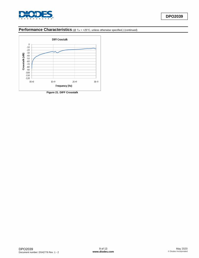
Performance Characteristics (@ TA = +25°C, unless otherwise specified.)
Figure 3. DIFF RDS(ON) Flatness
Figure 4. CC RDS(ON) Flatness
Figure 5. DIFFxC Leakage Current vs. Temperature
Figure 6. CCxC Leakage Current vs. Temperature
Figure 7. DIFFxC 5.5V OVP Leakage Current vs. Temperature
Figure 8. DIFFxC 22V OVP Leakage Current vs. Temperature
DIFF RDS(ON) Flatness, VVSYS = 4.2V CC RDS(ON) Flatness, VVSYS = 4.2V
Leakage Current, DIFFxC = 3.6V, VVSYS = 3.3V Leakage Current, CCxC = 5.5V, VVSYS = 3.3V
OVP Leakage Current, DIFFxC = 5.5V, VVSYS = 0V OVP Leakage Current, DIFFxC = 22V, VVSYS = 0V
Le
akag
e C
urr
en
t (μ
A)
Le
akag
e C
urr
en
t (μ
A)
OV
P L
eakag
e C
urr
en
t (μ
A)
OV
P L
eakag
e C
urr
en
t (μ
A)
RD
S(O
N) (Ω
)
RD
S(O
N) (Ω
)
-40°C
25°C
85°C
125°C
-40°C
25°C
85°C
125°C

DPO2039 Document number: DS42776 Rev. 1 - 2
7 of 13 www.diodes.com
May 2020 © Diodes Incorporated
DPO2039
Performance Characteristics (@ TA = +25°C, unless otherwise specified.) (continued)
Figure 9. DIFFxC OVP Leakage Current vs. Temperature
Figure 10. CCxC OVP Leakage Current vs. Temperature
Figure 11. DIFFxS OVP Leakage Current vs Temperature
Figure 12. CCxS OVP Leakage Current vs Temperature
Figure 13. VSYS Supply Current vs Temperature
OVP Leakage Current, DIFFxC = 5.5V, VVSYS = 0V OVP Leakage Current, CCxC = 22V, VVSYS = 0V
OVP Leakage Current, DIFFxC = 22V, VVSYS = 0V OVP Leakage Current, CCxC = 22V, VVSYS = 0V
VSYS Supply Current, VVSYS = 3.6V
Su
pp
ly C
urr
en
t (μ
A)
Figure 14. DIFF1C Short to 5V VBUS
DIF
Fx
S O
VP
Le
akag
e C
urr
en
t (μ
A)
CC
xS
OV
P L
eakag
e C
urr
en
t (μ
A)
OV
P L
eakag
e C
urr
en
t (μ
A)
OV
P L
eakag
e C
urr
en
t (μ
A)
DIFF1C
DIFF2C

DPO2039 Document number: DS42776 Rev. 1 - 2
8 of 13 www.diodes.com
May 2020 © Diodes Incorporated
DPO2039
Performance Characteristics (@ TA = +25°C, unless otherwise specified.) (continued)
Figure 15. DIFF1C Short to 24V VBUS
Figure 16. CC1C Short to 24V VBUS
Figure 17. DIFF MOSFET Turn-On Time
Figure 18. CC MOSFET Turn-On Time
Figure 19. DIFF Channel Bandwidth
Figure 20. CC Channel Bandwidth
DPO2039 Document number: DS42776 Rev. 1 - 2
9 of 13 www.diodes.com
May 2020 © Diodes Incorporated
DPO2039
Performance Characteristics (@ TA = +25°C, unless otherwise specified.) (continued)
Figure 21. DIFF Crosstalk
DPO2039 Document number: DS42776 Rev. 1 - 2
10 of 13 www.diodes.com
May 2020 © Diodes Incorporated
DPO2039
Application Information
General Description
The DPO2039 is a USB port protection device designed to work with USB Type-C connector, cable and USB PD to form a system that enables
signal management and power delivery in a compact package. It provides short to VBUS protection for the CC and DIFF pins over the USB Type-
C connector.
Short to VBUS Protection
The DPO2039 is a 4-channel uni-directional power switch with over-voltage protection. This is used to prevent the components inside a system
which adopts the USB Type-C connector from being damaged by unexpected hazard. On the USB Type-C connector, the CC and DIFF pins are
located in the close proximity of the VBUS pin. If ever the CC and/or the DIFF lines are short to the VBUS line either at the USB-C connector or at
the cable end, the components (mostly ICs manufactured on the various sub-micron process nodes) behind the USB Type-C connector can easily
be damaged by the resulting EOS. The damage, if occurred, is likely non-recoverable especially given that the voltage level on the VBUS line can
go up to 20V or slightly higher. The DPO2039 integrates four series over-voltage FETs to protect the system side CC and DIFF lines. When either
line on the Type-C connector side CC1C, CC2C, DIFF1C or DIFF2C is shorted to VBUS line, the DPO2039 will turn off the over-voltage FETs in
less than 100ns window to isolate the system side CC and DIFF lines from the over-voltage connector side. When shorted to VBUS line is
detected, the open-drain FAULTB will output low to indicate a fault condition.
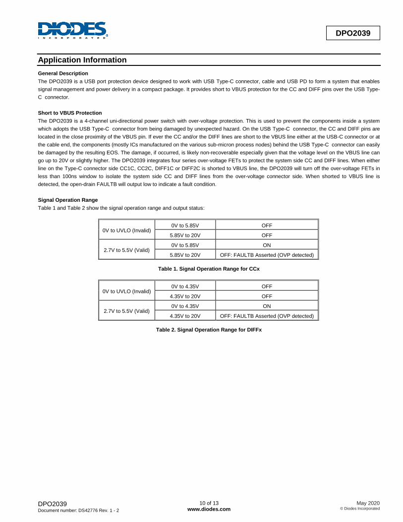
Signal Operation Range
Table 1 and Table 2 show the signal operation range and output status:
0V to UVLO (Invalid) 0V to 5.85V OFF
5.85V to 20V OFF
2.7V to 5.5V (Valid) 0V to 5.85V ON
5.85V to 20V OFF: FAULTB Asserted (OVP detected)
Table 1. Signal Operation Range for CCx
0V to UVLO (Invalid) 0V to 4.35V OFF
4.35V to 20V OFF
2.7V to 5.5V (Valid) 0V to 4.35V ON
4.35V to 20V OFF: FAULTB Asserted (OVP detected)
Table 2. Signal Operation Range for DIFFx

DPO2039 Document number: DS42776 Rev. 1 - 2
11 of 13 www.diodes.com
May 2020 © Diodes Incorporated
DPO2039
Ordering Information (Note 7)
DPO2039 X - X
PackingPackage
13 : 13'' Tape & ReelDAB : U-QFN3030-16
(Type B)
Part Number Marking ID Reel Size (inches) Tape Width (mm) 13” Tape and Reel
Quantity Part Number Suffix
DPO2039DAB-13 PO39 13 8 3,000/Tape & Reel -13
Note: 7. For packaging details, go to our website at https://www.diodes.com/design/support/packaging/diodes-packaging/.
Marking Information
Pin 1 Logo
Marking ID Date Code
PO39
YY WW
YY: Year WW: Week 01 to 53

DPO2039 Document number: DS42776 Rev. 1 - 2
12 of 13 www.diodes.com
May 2020 © Diodes Incorporated
DPO2039
Package Outline Dimensions
Please see http://www.diodes.com/package-outlines.html for the latest version.
U-QFN3030-16 (Type B)
Side View
AA3A1
Bottom View
D
D2
E
e
b (16x)
L (16x)
E2
(Pin #1 ID)
Z (8x)
0.450R0.200
Suggested Pad Layout
Please see http://www.diodes.com/package-outlines.html for the latest version.
U-QFN3030-16 (Type B)
Mechanical Data
Moisture Sensitivity: Level 1 per J-STD-020
Terminals: NiPdAu Finish, Solderable per MIL-STD-202, Method 208
Weight: 0.0167 grams (Approximate)
U-QFN3030-16
Type B Dim Min Max Typ
A 0.55 0.65 0.60
A1 0 0.05 0.02
A3 - - 0.15
b 0.18 0.28 0.23
D 2.95 3.05 3.00
D2 1.40 1.60 1.50
E 2.95 3.05 3.00
E2 1.40 1.60 1.50
e - - 0.50
L 0.35 0.45 0.40
Z - - 0.625
All Dimensions in mm
Dimensions Value
(in mm)
C 0.500
G 0.150
G1 0.150
X 0.350
X1 1.800
Y 0.600
Y1 1.800
X (16x)
Y (16x)
C
Y1
X1
G1
G
DPO2039 Document number: DS42776 Rev. 1 - 2
13 of 13 www.diodes.com
May 2020 © Diodes Incorporated
DPO2039
IMPORTANT NOTICE DIODES INCORPORATED MAKES NO WARRANTY OF ANY KIND, EXPRESS OR IMPLIED, WITH REGARDS TO THIS DOCUMENT, INCLUDING, BUT NOT LIMITED TO, THE IMPLIED WARRANTIES OF MERCHANTABILITY AND FITNESS FOR A PARTICULAR PURPOSE (AND THEIR EQUIVALENTS UNDER THE LAWS OF ANY JURISDICTION). Diodes Incorporated and its subsidiaries reserve the right to make modifications, enhancements, improvements, corrections or other changes without further notice to this document and any product described herein. Diodes Incorporated does not assume any liability arising out of the application or use of this document or any product described herein; neither does Diodes Incorporated convey any license under its patent or trademark rights, nor the rights of others. Any Customer or user of this document or products described herein in such applications shall assume all risks of such use and will agree to hold Diodes Incorporated and all the companies whose products are represented on Diodes Incorporated website, harmless against all damages. Diodes Incorporated does not warrant or accept any liability whatsoever in respect of any products purchased through unauthorized sales channel. Should Customers purchase or use Diodes Incorporated products for any unintended or unauthorized application, Customers shall indemnify and hold Diodes Incorporated and its representatives harmless against all claims, damages, expenses, and attorney fees arising out of, directly or indirectly, any claim of personal injury or death associated with such unintended or unauthorized application. Products described herein may be covered by one or more United States, international or foreign patents pending. Product names and markings noted herein may also be covered by one or more United States, international or foreign trademarks. This document is written in English but may be translated into multiple languages for reference. Only the English version of this document is the final and determinative format released by Diodes Incorporated.
LIFE SUPPORT Diodes Incorporated products are specifically not authorized for use as critical components in life support devices or systems without the express written approval of the Chief Executive Officer of Diodes Incorporated. As used herein: A. Life support devices or systems are devices or systems which: 1. are intended to implant into the body, or
2. support or sustain life and whose failure to perform when properly used in accordance with instructions for use provided in the labeling can be reasonably expected to result in significant injury to the user.
B. A critical component is any component in a life support device or system whose failure to perform can be reasonably expected to cause the failure of the life support device or to affect its safety or effectiveness. Customers represent that they have all necessary expertise in the safety and regulatory ramifications of their life support devices or systems, and acknowledge and agree that they are solely responsible for all legal, regulatory and safety-related requirements concerning their products and any use of Diodes Incorporated products in such safety-critical, life support devices or systems, notwithstanding any devices- or systems-related information or support that may be provided by Diodes Incorporated. Further, Customers must fully indemnify Diodes Incorporated and its representatives against any damages arising out of the use of Diodes Incorporated products in such safety-critical, life support devices or systems. Copyright © 2020, Diodes Incorporated www.diodes.com