DPI Immunity Modeling of a Low Dropout Voltage...
9
Immunity of a Voltage Regulator IC-EMC Application note Page 1 DPI Immunity Modeling of a Low Dropout Voltage Regulator A. Cisse Ndoye (1) , Wu Jianfei (2) , F. Lafon (3) , E. Sicard (1) (1) INSA-GEI, 135 Av de Rangueil 31077 Toulouse – France (2) School of Electronic Science and Engineering, NUDT, Changsha, Hunan, 410073, China (3) VALEO VECS, 2 Rue Fernand Pouillon, 94042 Créteil Cedex, France Contact : [email protected] – web site : www.ic-emc.org Abstract: The susceptibility of a low dropout voltage regulator (LDO) in direct power injection (DPI) is analyzed by measurements and simulation. The measurements highlight the offset in the output induced by the conducted RF disturbances and various failure modes. Discrete components used in the injection path and test board are modeled based on impedance measurements. DPI simulations using simple and complex models are presented, which highlight the strongly non-linear behavior of the circuit even at low levels of power injection. The comparison between measurement and results of different models is given. And the reasons for the diversity of immunity level in frequency domain are analyzed. This work has been conducted by A. Cisse Ndoye, PhD student of the French project “EPEA- Aerospace Valley” (2007-2010) funded by the French Ministry of Industry, in cooperation with F. Lafon, VALEO, France, and by Wu Jianfei, PhD student from NUDT Changsha, China, funded by the Chinese Government. Keywords: DPI; Conducted RF disturbances; Model; Immunity; Frequency domain Directory in IC-EMC (version 2.5): case_study/l4949 1 Introduction This application note addresses the immunity of an Low-Dropout (LDO) 5 V regulator and its modeling [1]. Based on impedance and Direct-Power-Injection (DPI) measurements [2], the objective of our work is to propose a simple and accurate model of the regulator and its surrounding discrete components, for further use of printed-circuit-board (PCB) level EMC prediction. The device under test (DUT) used in our investigations is a low-power regulator designed for supplying microcontrollers in embedded applications, typically automotive electronic sub-systems. The regulator features an output voltage precision around ±1% at 5 V. Section 2 explains our measurement and modeling flow in general terms. In Section 3 the impedance measurements for discrete on-board devices and for the L4949 are presented. These DPI measurements are exploited in Section 4, where several models are introduced and simulated with increased structural complexity. An efficient non-linear approach for macro modeling is presented, based on the Spice “B-element”. 2 DPI Setup The DPI measurement setup used in the L4949 study is shown in Fig. 1. It includes the DUT board designed by F. Lafon [4], the EMI injection (Signal generator, amplifier, coupler and power meter), the DC voltage source, on-board bias tees and failure monitoring. The measurement is carried out according to the IEC 62132- 4 “DPI” standard [2]. The test setup is controlled by a Labview software.
Transcript of DPI Immunity Modeling of a Low Dropout Voltage...
Immunity of a Voltage Regulator
IC-EMC Application note Page 1
DPI Immunity Modeling of a Low Dropout Voltage Regu lator
A. Cisse Ndoye(1), Wu Jianfei(2), F. Lafon(3), E. Sicard(1) (1)INSA-GEI, 135 Av de Rangueil
31077 Toulouse – France (2) School of Electronic Science and Engineering, NUDT, Changsha, Hunan, 410073, China
(3) VALEO VECS, 2 Rue Fernand Pouillon, 94042 Créteil Cedex, France
Contact : [email protected] – web site : www.ic-emc.org
Abstract: The susceptibility of a low dropout voltage regulator (LDO) in direct power injection (DPI) is analyzed by measurements and simulation. The measurements highlight the offset in the output induced by the conducted RF disturbances and various failure modes. Discrete components used in the injection path and test board are modeled based on impedance measurements. DPI simulations using simple and complex models are presented, which highlight the strongly non-linear behavior of the circuit even at low levels of power injection. The comparison between measurement and results of different models is given. And the reasons for the diversity of immunity level in frequency domain are analyzed.
This work has been conducted by A. Cisse Ndoye, PhD student of the French project “EPEA-Aerospace Valley” (2007-2010) funded by the French Ministry of Industry, in cooperation with F. Lafon, VALEO, France, and by Wu Jianfei, PhD student from NUDT Changsha, China, funded by the Chinese Government.
Keywords: DPI; Conducted RF disturbances; Model; Immunity; Frequency domain
Directory in IC-EMC (version 2.5): case_study/l4949
1 Introduction
This application note addresses the immunity of an Low-Dropout (LDO) 5 V regulator and its modeling [1]. Based on impedance and Direct-Power-Injection (DPI) measurements [2], the objective of our work is to propose a simple and accurate model of the regulator and its surrounding discrete components, for further use of printed-circuit-board (PCB) level EMC prediction.
The device under test (DUT) used in our investigations is a low-power regulator designed for supplying microcontrollers in embedded applications, typically automotive electronic sub-systems. The regulator features an output voltage precision around ±1% at 5 V.
Section 2 explains our measurement and modeling flow in general terms. In Section
3 the impedance measurements for discrete on-board devices and for the L4949 are presented. These DPI measurements are exploited in Section 4, where several models are introduced and simulated with increased structural complexity. An efficient non-linear approach for macro modeling is presented, based on the Spice “B-element”.
2 DPI Setup
The DPI measurement setup used in the L4949 study is shown in Fig. 1. It includes the DUT board designed by F. Lafon [4], the EMI injection (Signal generator, amplifier, coupler and power meter), the DC voltage source, on-board bias tees and failure monitoring. The measurement is carried out according to the IEC 62132-4 “DPI” standard [2]. The test setup is controlled by a Labview software.

Immunity of a Voltage Regulator
IC-EMC Application note Page 2
Figure 1 : The DPI test-bench
Figure 2 : The test board developed by F. Lafon [4], VALEO, and a zoom at the DUT
(L4949)
The program controls the power injected to the DUT, the frequency of the RFI, and the failure criterion.
3 Discrete Component models
The discrete components used in the PCB board for a nominal operation of the L4949 regulator and the DPI injection are characterized by the VNA in order to extract their impedance variation with frequency, within the range [1-3000 MHz]. From these results, models are extracted for each component that may have a direct impact on the DPI measurements and models [3]. The set of components is illustrated in Fig. 3.
10 kR_reset
DCL_ferrite1 L_ferrite2
47 uHL_47uH
1 nFC_dpi
Ferrite
L4949
VCC
SI
VZ
CT
VOUT
SO
RESET
GND
10 uFC_load
VNA
50R_match
12 V
S1
S2
Figure 3 : Discrete components used for the
DPI setup and nominal operation of the L4949 regulator
Table 1 gives the list of discrete components present in the board. The most important components to be characterized are C_dpi, L_47uH and L_ferrite.
TABLE I. DISCRETE COMPONENTS USED IN THE PCB TEST BOARD
Model Parts Symbol Comments RF Injection path
Capacitor C_dpi 1 nF GRM1885C1H102JA
DC input
Inductor L_47uH 47 µH B82422A1473K
Ferrite*2 L_ferrite Murata BLM18HK102SN1
Package
Lead R_lead, L_ lead ,C_ lead
VCC, VOUT and GND
Bonding R_bond, L_ bond ,C_ bond
VCC, VOUT and GND
Load Capacitor C_load Capacitor for load Resistor R_load Resistor for load
Reset Resistor R_reset Reset resistor
3.1 DPI path model
To model the injection path, we need to take into account the 1-nF capacitance and the 17-mm length PCB track from the SMA conductor to the capacitance. The PCB board includes a specific pattern, shown in fig. 4, which eases the impedance characterization of the injection path.

Immunity of a Voltage Regulator
IC-EMC Application note Page 3
1 nF DPI Capa
PCB track from injection connector to DPI capa
Figure 4 : The DPI injection path includes a portion of PCB and a 1-nF capacitance
The model of the injection path is composed of a 34 Ω transmission line and a RLC circuit that models the 1 nF DPI capacitance (Fig. 5). The transmission line do not take into account losses. An alternative is to build a T-model as described below, which includes serial losses (here a 0.1 Ω resistance). Figure 6 shows a good correlation between measurement and simulation of the impedance from 1 MHz to 3 GHz.
To further improve the marching, the transmission line may to be split. We use the tool “Interconnect parameters” (Fig. 7), extend the cut-off frequency to 6 GHz, and choose the interconnect model and associated dimensions as close as the board used for DPI experiments.
Figure 5 : Building a model for the DPI injection
capacitance (Zin_DPI_1nF.sch)
Figure 6 : Matching the injection path
impedance with measurements (Zin_DPI_1nF.sch vs Zin_dpi_1nF.s)
Figure 7 : Use of Interconnect Parameters to build a TLine model valid upto 6 GHz
Unchanged SMA model
3 cells needed to match [s] measurements upto 6 GHz
Unchanged DPI capacitance model
Figure 8 : Improved model to match measurements upto 6 GHz
(Zin_DPI_1nF_xhf.sch)

Immunity of a Voltage Regulator
IC-EMC Application note Page 4
Figure 9 : Improved matching upto 6 GHz (Zin_DPI_1nF_xhf.sch vs Zin_DPI_1nF.s)
Fig. 8 gives a xHF model of the 17-mm interconnect, using 3 R-L-C cells instead of one single cell. As may be seen in Fig. 9, the matching of the Z(f) injection path is improved upto 6 GHz.
3.2 Inductance model
A high frequency model of the 47µH inductance is proposed in Fig. 10. It can be seen that the main resonance (12 MHz) is well predicted, but the high frequency fluctuations (500, 800 MHz) are not handled by the proposed model (Fig. 11).
Figure 10: Building a model for the 47uF
discrete inductance (Zin_L47u.sch)
Figure 11: Matching the model with measurements for 47uF inductance (
Zin_L47u.sch vs Zin_L47u.s50)
3.3 Ferrite model
Fig. 12 details the ferrite model used by F. Lafon [3][4] to match simulations with Z(f) measurements. In a first order approach, the ferrite may be considered as a simple resistance, ranging from 100 to 1000 Ω, with an average value close to 200 Ω. The measured ferrite impedance has a very unusual shape (Fig. 13), far from classical 20 dB/decade behaviors found in L or C components. The impedance ranges from 100 to 1000 Ω. The approach used by F. Lafon [4] is based on a network of coupled R/L circuits, an approach close to the skin-effect modeling described in IC-EMC manual “Appendix – EMC model library – Skin Effect Model”. More information about the ferrite model may also be found in the “Appendix – EMC model library – Inductor and Ferrite Model”

Immunity of a Voltage Regulator
IC-EMC Application note Page 5
Figure 12: The model of Murata
BLM18HK102SN1 (Zin_Ferrite.sch)
Figure 13 : Matching the model with
measurements for the ferrite (Zin_Ferrite.sch)
3.3.1 IC Impedance measurements
The impedance measurement of the L4949 device is described in [1]. The L4949 is supplied either at 0 V or at nominal 12 V supply. A Vector network analyzer (VNA) is calibrated using short, open and 50 Ω loads prior to Z(f) measurements. More information may be also found in [5].
Figure 14: The VNA used for Z(f) measurements
Bias dependant capacitance variation
Bias independant L,C contributions
Non linear junction capacitance
Linear PCB/package/die impedance
Figure 15: Impedance measurement of the L4949 regulator (VCC pin to ground) with 0V and 12V DC supply (L4949_ZOfF_RF_0V.z,
L4949_ZOfF_RF_12V.z)
From the measurements reported in Fig. 15, we clearly see a dependence of the impedance versus the DC voltage at low frequencies (1-10 MHz), while the impedance is almost independent of the DC supply above 10 MHz. The explanation may be a dominant contribution of junction-based bias-dependent capacitance (1-10 MHz) and passive bias-independent L,C at high frequencies.

Immunity of a Voltage Regulator
IC-EMC Application note Page 6
4 DPI modeling
4.1 DPI measurements
The immunity criterion is observed at the output of the regulator. The Vout drift larger than +/- 200 mV is considered as a fault. The voltage monitoring is performed by an oscilloscope, using a voltage mask at 4.8-5.2 V. Fig. 16 illustrates the case of a 100 MHz RFI at 12.9 dBm incident power. The RFI superimposed to the L4949 input VCC (12 V) appears in an attenuated and distorted form on the Vout pin, with a DC shift and a voltage lower than 4.8 V.
Figure 16: Example of fault: the output voltage (5.0V nominal) decreases down to 4.8 V (RFI
at 100 MHz).
4.2 A very simple DPI Model – Model A
The regulating device is firstly considered as a resistor, with a value adjusted to obtain a nominal output voltage of 5V. The regulator model shown in Fig. 17 only consists of a simple resistor (88 Ω), capacitor (27 pF) and the package inductors (1 nH). The DC supply of 12V and the RF injection system are added in a simplified way. The ferrite is assumed to be around 220 Ω, which correspond to the average module of Z(f). The loads are placed according to the board design.
Fig 17: Simple model “A” (L4949_modelA.sch)
The 10 uF capacitor is mandatory for the regulator stability, while the 220 Ω serial resistance represents a resistive load.
The test point is the output of the regulator, which is monitored using an active probe, with a negligible parasitic capacitance (4.7 pF) as compared to the 10 uF capacitor.
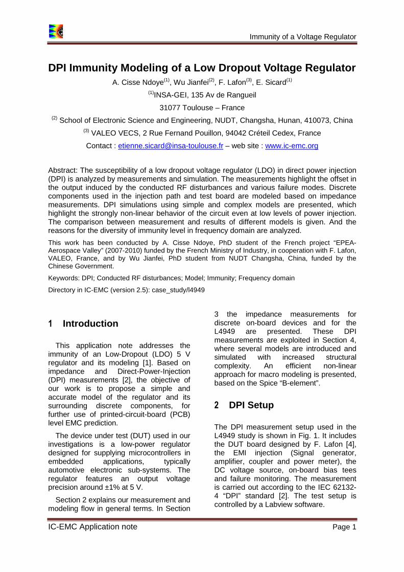
We configure the RFI in automatic mode, with a frequency range from 1 to 2000 MHz, a log scale, 10 points per decade, and a maximum power of 40 dBm. We also define a voltage failure above 5.2V and below 4.8 V. The set up is as follows:
• Click “Generate Spice” • Launch WinSpice, run the 34
simulations in a row • Click “Simulation Control file”, click
“RFIcontrol_L4949_modelA.ctl” • Click « Get power » • Click “Add forward power”
In this situation, there is no non-linear device, so no rectification effect, and as we have placed a perfect decoupling of 10uF, no susceptibility criteria is matched for the whole frequency bandwidth (Fig. 19).
Immunity of a Voltage Regulator
IC-EMC Application note Page 7
Fig 18: Setting the RFI simulation mode in
automatic mode, and running associated 34 simulations using WinSpice
(L4949_modelA.sch)
Fig 19: DPI simulation of model “A”
(L4949_modelA.sch vs. L4949_DPI_Measurement.tab)
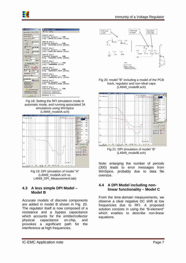
4.3 A less simple DPI Model – Model B
Accurate models of discrete components are added in model B shown in Fig. 20. The regulator itself is now composed of a resistance and a bypass capacitance which accounts for the emitter/collector physical capacitance on-chip, and provokes a significant path for the interference at high frequencies.
PCB track to DPI
PCB track to loads
Non-ideal 10u Capa
Fig 20: model “B” including a model of the PCB track, regulator and non-ideal capa
(L4949_modelB.sch)
Fig 21: DPI simulation of model “B”
(L4949_modelB.sch)
Note: enlarging the number of periods (300) leads to error messages from WinSpice, probably due to data file oversize.
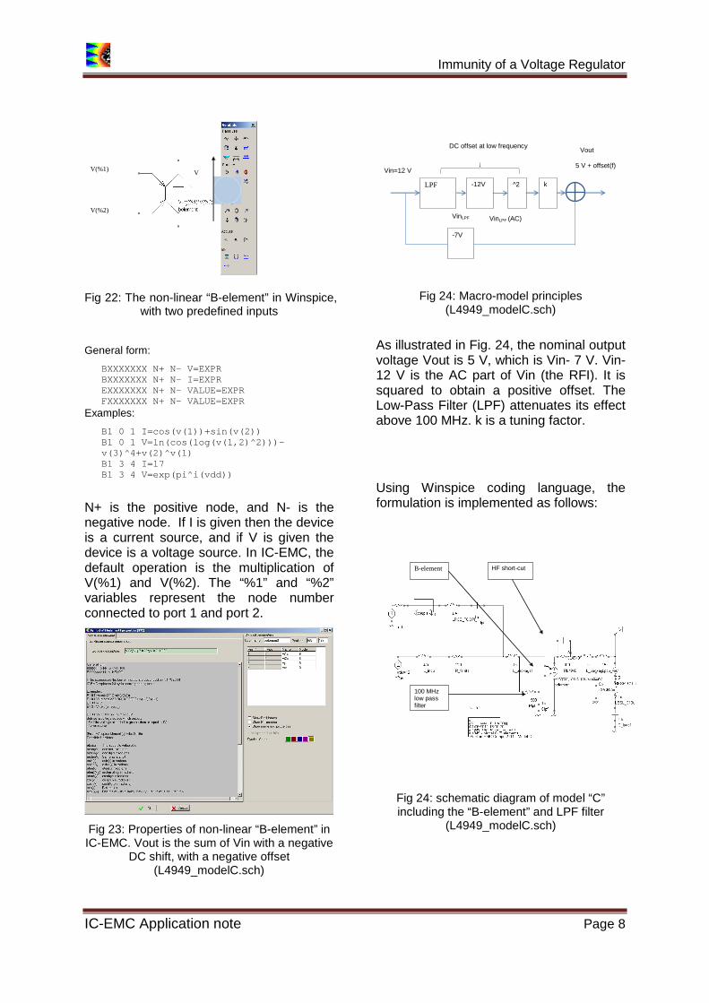
4.4 A DPI Model including non-linear functionality – Model C
From the time-domain measurements, we observe a clear negative DC shift at low frequencies due to RFI. A proposed solution consists in using the “B-element” which enables to describe non-linear equations.
Immunity of a Voltage Regulator
IC-EMC Application note Page 8
V(%1)
V(%2)
V
Fig 22: The non-linear “B-element” in Winspice,
with two predefined inputs
General form:
BXXXXXXX N+ N- V=EXPR BXXXXXXX N+ N- I=EXPR EXXXXXXX N+ N- VALUE=EXPR FXXXXXXX N+ N- VALUE=EXPR
Examples:
B1 0 1 I=cos(v(1))+sin(v(2)) B1 0 1 V=ln(cos(log(v(1,2)^2)))-v(3)^4+v(2)^v(1) B1 3 4 I=17 B1 3 4 V=exp(pi^i(vdd))
N+ is the positive node, and N- is the negative node. If I is given then the device is a current source, and if V is given the device is a voltage source. In IC-EMC, the default operation is the multiplication of V(%1) and V(%2). The “%1” and “%2” variables represent the node number connected to port 1 and port 2.
Fig 23: Properties of non-linear “B-element” in IC-EMC. Vout is the sum of Vin with a negative
DC shift, with a negative offset (L4949_modelC.sch)
LPF
-7V
^2 k
DC offset at low frequency
Vin=12 V 5 V + offset(f)
VinLPF
Vout
-12V
VinLPF (AC)
Fig 24: Macro-model principles
(L4949_modelC.sch)
As illustrated in Fig. 24, the nominal output voltage Vout is 5 V, which is Vin- 7 V. Vin-12 V is the AC part of Vin (the RFI). It is squared to obtain a positive offset. The Low-Pass Filter (LPF) attenuates its effect above 100 MHz. k is a tuning factor.
Using Winspice coding language, the formulation is implemented as follows:
B-element HF short-cut
100 MHz low pass filter
Fig 24: schematic diagram of model “C” including the “B-element” and LPF filter
(L4949_modelC.sch)

Immunity of a Voltage Regulator
IC-EMC Application note Page 9
Fig 25: DPI simulation of model “C” (L4949_modelC.sch vs.
L4949_DPI_Measurement.tab)
The simulation shown Fig. 25 features a good match with the measurement, for k fixed to -0.25. As stated in [1], the non-linear B-element handles the “in-band” mode. In other words, the L4949 really acts as a regulator up to 50 MHz. From 1 to 50 MHz, Vout is controlled by the negative feedback circuit and the L4949 is very sensitive to RFI. The non-linear expression combined with a low-pass filter is an efficient approach to reproduce the “in-band” mode.
References
[1] Wu Jian-fei, E. Sicard, A. Cissé Ndoye, F. Lafon, Li Jian-cheng, Shen Rong-jun, "Investigation on DPI Effects in a Low Dropout Voltage Regulator", EMC Compo 2011, Dubrovnick, Croatia, November 2011
[2] IEC 623132-4: Integrated Circuits, Measurement of Electromagnetic Immunity – Part 4: Direct RF Power Injection Method
[3] F. Lafon, F. de Daran, M. Ramdani and R. Perdriau and M.Drissi, “Immunity Modeling of Integrated Circuits: an Industrial Case,” in IEICE Transactions on Communications, Volume: E93-B, NO. 7, July 2010, pp. 1723-1730.
[4] F. Lafon, "Développement de techniques et de méthodologies pour la prise en compte des contraintes CEM dans la conception d'équipements du domaine automobile. Etude de l'immunité, du composant à l'équipement." – PhD report, Jan. 2011 (in French) http://sites.google.com/site/fredericlafonemc
[5] A. C. Ndoye "Contribution à la modélisation de l'immunité conduite des circuits intégrés et étude de l'impact du vieillissement sur leur compatibilité électromagnétique », PhD report, N°1049, Oct 2010 (in French), http://eprint.insa-toulouse.fr/archive/00000360


![The effects of nonnormality on asymptotic …Let uabbe the (a,b)th element of a p× psymmetric matrix U . Then, we consider two types of vectors, vec (U)and vecs (U)(see [6, p. 272]),](https://static.fdocuments.in/doc/165x107/5ecba8680845f01b645f3098/the-effects-of-nonnormality-on-asymptotic-let-uabbe-the-abth-element-of-a-p.jpg)