DPF 2013 R. Kass 1 P. Buchholz, M. Ziolkowski Universität Siegen OUTLINE Lessons learned…...
19
DPF 2013 R. Kass 1 R. Kass P. Buchholz, M. Ziolkowski Universität Siegen OUTLINE Lessons learned… IBL/nSQP opto-board overview assembly experience radiation hardness production Summary/Conclusions K.K. Gan, H.P. Kagan, R.D. Kass, J. Moss, J. Moore, S. Smith, Y. Yang The Ohio State University
-
Upload
ferdinand-douglas -
Category
Documents
-
view
215 -
download
1
Transcript of DPF 2013 R. Kass 1 P. Buchholz, M. Ziolkowski Universität Siegen OUTLINE Lessons learned…...

DPF 2013R. Kass 1R. Kass
P. Buchholz, M. ZiolkowskiUniversität Siegen
OUTLINELessons learned…IBL/nSQP opto-board
overviewassembly experienceradiation hardnessproduction
Summary/Conclusions
K.K. Gan, H.P. Kagan, R.D. Kass, J. Moss, J. Moore, S. Smith, Y. Yang
The Ohio State University
DPF 2013
R. Kass
2
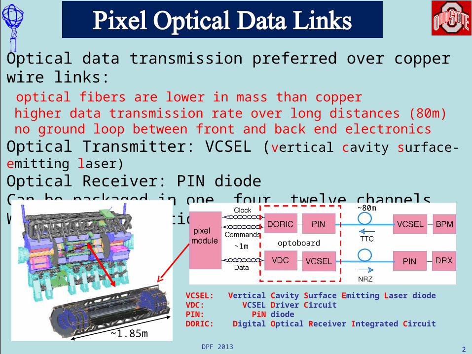
Optical data transmission preferred over copper wire links: optical fibers are lower in mass than copper higher data transmission rate over long distances (80m) no ground loop between front and back end electronicsOptical Transmitter: VCSEL (vertical cavity surface-emitting laser)Optical Receiver: PIN diodeCan be packaged in one, four, twelve channelsWork in the radiation environment of the LHC
~1.85m
~80m
optoboard ~1m
VCSEL: Vertical Cavity Surface Emitting Laser diodeVDC: VCSEL Driver CircuitPIN: PiN diodeDORIC: Digital Optical Receiver Integrated Circuit

DPF 2013R. Kass IEEE04/Rome 3
The pre-IBL Opto-board Optical signal electrical signal conversion occurs here
Contains 7 optical links, each link serving one Pixel module
Fabricated in 2 flavors– Layer B: for inner barrel, 2 data links per module for high
occupancy – Layer D: for outer barrel and disks 1 and 2
Fabricated with BeO for heat management
44 B boards228 D boards
Opto-pack
Housing
Pin array
DORIC
VCSEL array
VDC
DPF 2013
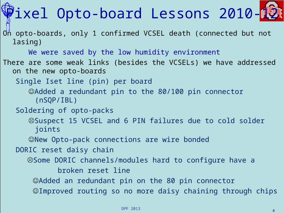
On opto-boards, only 1 confirmed VCSEL death (connected but not lasing)
We were saved by the low humidity environmentThere are some weak links (besides the VCSELs) we have addressed
on the new opto-boardsSingle Iset line (pin) per board
Added a redundant pin to the 80/100 pin connector (nSQP/IBL)
Soldering of opto-packsSuspect 15 VCSEL and 6 PIN failures due to cold solder jointsNew Opto-pack connections are wire bonded
DORIC reset daisy chain Some DORIC channels/modules hard to configure have a broken reset line
Added an redundant pin on the 80 pin connector Improved routing so no more daisy chaining through chips
Pixel Opto-board Lessons 2010-12
4
DPF 2013
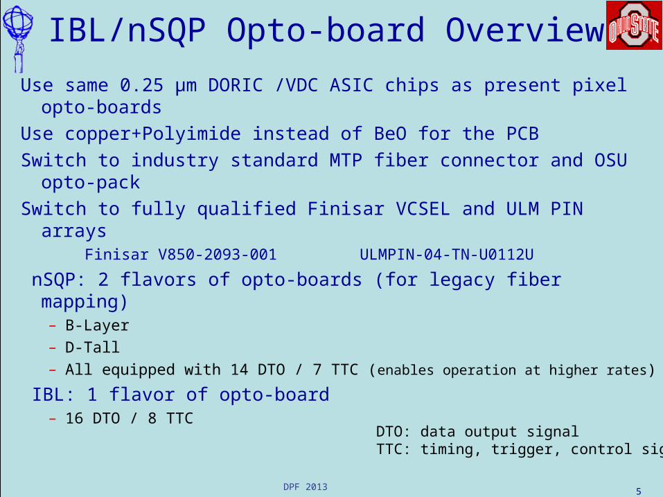
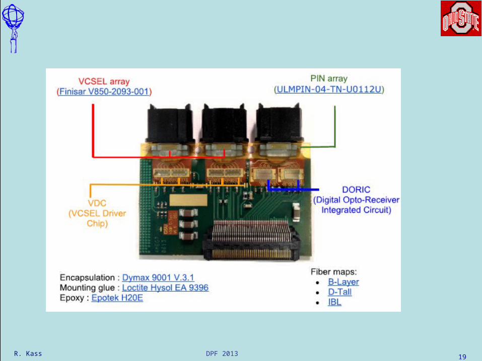
Use same 0.25 µm DORIC /VDC ASIC chips as present pixel opto-boards
Use copper+Polyimide instead of BeO for the PCBSwitch to industry standard MTP fiber connector and OSU
opto-packSwitch to fully qualified Finisar VCSEL and ULM PIN arrays Finisar V850-2093-001 ULMPIN-04-TN-U0112U
nSQP: 2 flavors of opto-boards (for legacy fiber mapping)– B-Layer– D-Tall– All equipped with 14 DTO / 7 TTC (enables operation at higher
rates)
IBL: 1 flavor of opto-board– 16 DTO / 8 TTC
IBL/nSQP Opto-board Overview
5
DTO: data output signalTTC: timing, trigger, control signal

DPF 2013
nSQP/IBL Opto-Board Prototyping
We have constructed10 nSQP B-boards 5 for irradiation 5 for system tests (2 to CERN 1 to SLAC, 1 to BERN, 1 to
Wuppertal) 6 nSQP D-boards All for system tests (4 to CERN) 2 failed QA
1 with bad wire-bonds1 with a bad DORIC (slipped through test in 2005)
6 IBL boardsAll for system tests (5 to CERN, 1 to SLAC)
No complaints received on distributed boards
6
DPF 2013
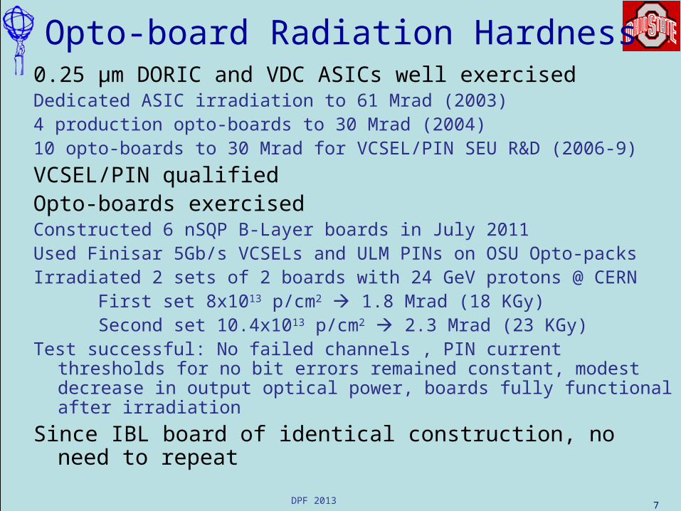
0.25 μm DORIC and VDC ASICs well exercisedDedicated ASIC irradiation to 61 Mrad (2003)4 production opto-boards to 30 Mrad (2004) 10 opto-boards to 30 Mrad for VCSEL/PIN SEU R&D (2006-9)
VCSEL/PIN qualifiedOpto-boards exercisedConstructed 6 nSQP B-Layer boards in July 2011Used Finisar 5Gb/s VCSELs and ULM PINs on OSU Opto-packsIrradiated 2 sets of 2 boards with 24 GeV protons @ CERN
First set 8x10¹³ p/cm2 1.8 Mrad (18 KGy)Second set 10.4x10¹³ p/cm2 2.3 Mrad (23 KGy)
Test successful: No failed channels , PIN current thresholds for no bit errors remained constant, modest decrease in output optical power, boards fully functional after irradiation
Since IBL board of identical construction, no need to repeat
Opto-board Radiation Hardness
7
DPF 2013
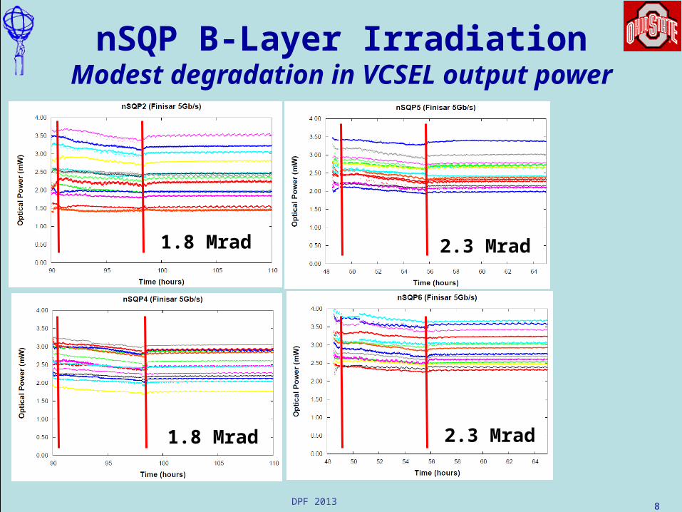
nSQP B-Layer IrradiationModest degradation in VCSEL output
power
8
1.8 Mrad
1.8 Mrad
2.3 Mrad
2.3 Mrad
DPF 2013
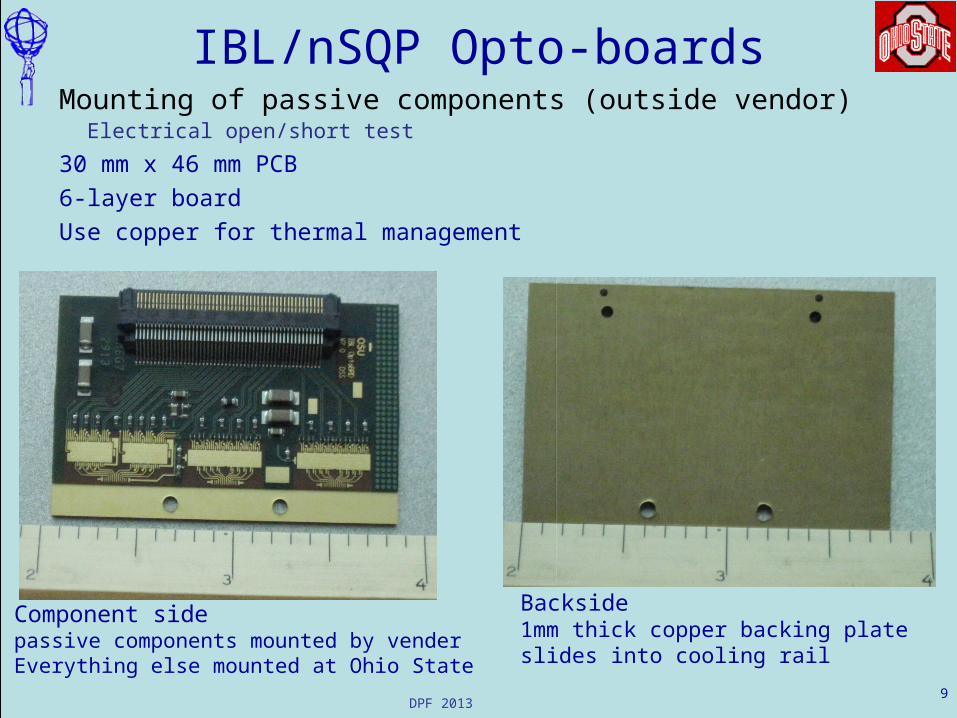
IBL/nSQP Opto-boardsMounting of passive components (outside vendor) Electrical open/short test
30 mm x 46 mm PCB6-layer boardUse copper for thermal management
9
Component sidepassive components mounted by venderEverything else mounted at Ohio State
Backside1mm thick copper backing plate slides into cooling rail

DPF 2013
Opto-Pack Production
10
SubstrateBeO for VCSELs (thermal management)Alumina for PINs
Opto-pack holds a VCSEL or PIN arrayAlignment of fiber to PIN/VCSEL is critical
“bare” opto-pack and guide pins
gluing guide pins into opto-pack
opto-pack with guide pins

DPF 2013
Opto-Pack Production
11
dust cover installedwire bonding to PIN/VCSEL
wire bonded PIN/VCSEL arrayPIN/VCSEL array glued to opto-pack
Produce opto-packs (2 VCSEL, 1 PIN per opto-board)PIN/VCSEL array must be put on Opto-pack & connected to tracesVCSEL QA: LIV, reverse bias looking for ESDPIN QA: dark current, illuminate with 1mW & measure responsivity, check specs
1
2
3
4
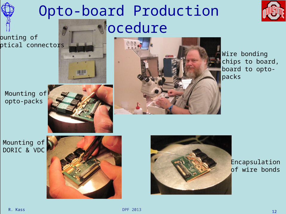
DPF 2013R. Kass 12
Wire bonding chips to board, board to opto-packs
Opto-board Production Procedure
Mounting of opto-packs
Encapsulation of wire bonds
Mounting of optical connectors
Mounting ofDORIC & VDC
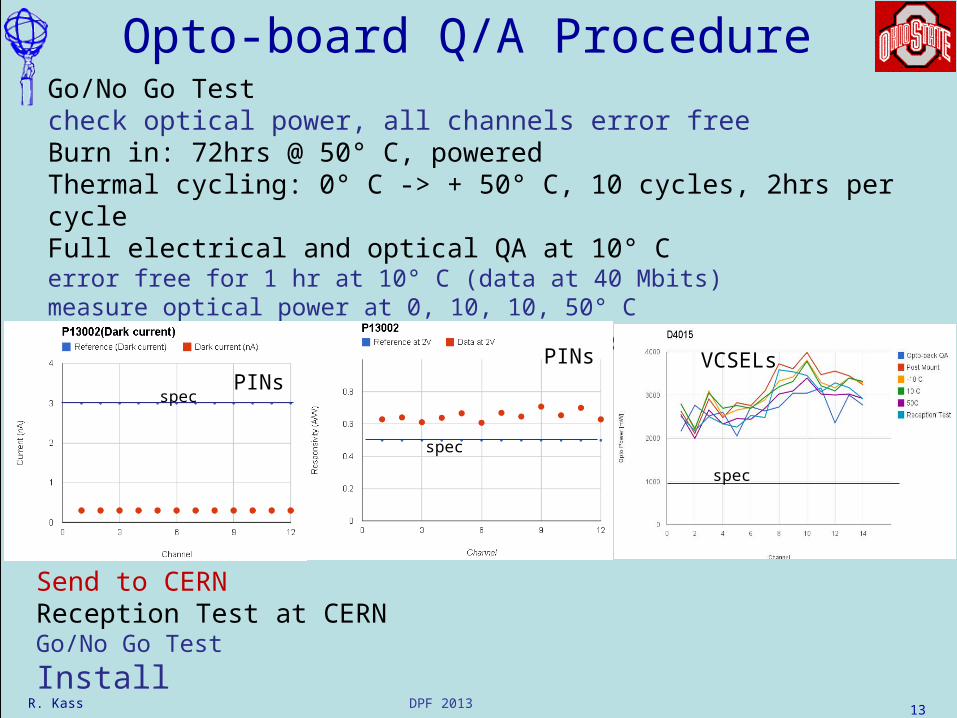
DPF 2013R. Kass 13
Go/No Go Testcheck optical power, all channels error freeBurn in: 72hrs @ 50° C, poweredThermal cycling: 0° C -> + 50° C, 10 cycles, 2hrs per cycleFull electrical and optical QA at 10° C error free for 1 hr at 10° C (data at 40 Mbits)measure optical power at 0, 10, 10, 50° Ccheck LVDS, jitter, rise/fall time, duty cycle
Opto-board Q/A Procedure
Send to CERNReception Test at CERNGo/No Go Test
Install
PINsPINs VCSELs
spec
spec
spec

DPF 2013R. Kass 14
Completed Opto-board
PIN
cooling from here (top rail)
VCSEL
VCSEL
MTPFiber
Connector
opto-pack
VDC
DORIC
30 mm
DPF 2013
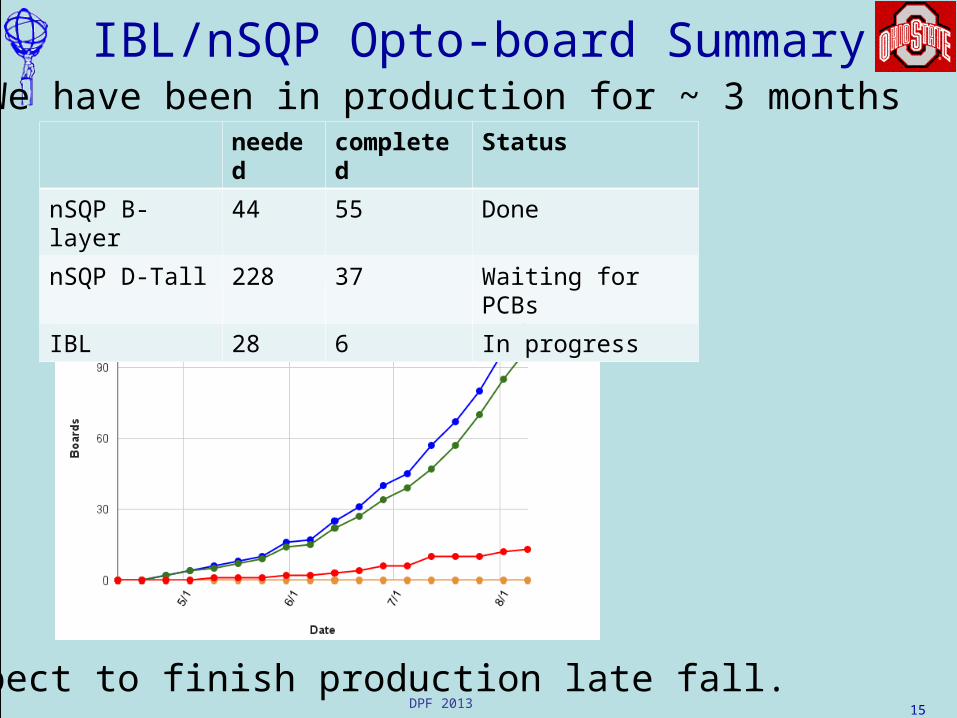
IBL/nSQP Opto-board Summary
15
We have been in production for ~ 3 months
Expect to finish production late fall.
needed
completed
Status
nSQP B-layer 44 55 Done
nSQP D-Tall 228 37 Waiting for PCBs
IBL 28 6 In progress
DPF 2013R. Kass 16
Extra Slides
DPF 2013R. Kass IEEE04/Rome 17
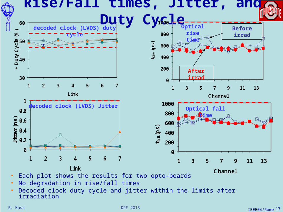
Rise/Fall times, Jitter, and Duty Cycle
• Each plot shows the results for two opto-boards• No degradation in rise/fall times• Decoded clock duty cycle and jitter within the limits after irradiation
Optical rise time
decoded clock (LVDS) duty cycle
Optical fall time
decoded clock (LVDS) Jitter
After irrad
Before irrad
DPF 2013
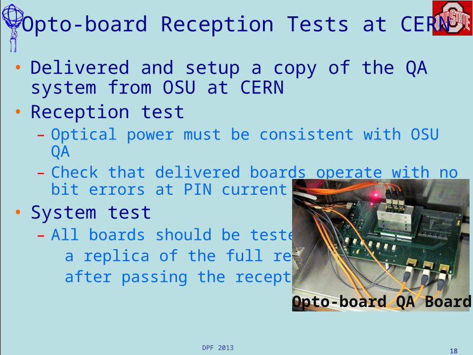
• Delivered and setup a copy of the QA system from OSU at CERN
• Reception test– Optical power must be consistent with OSU QA– Check that delivered boards operate with no bit errors at
PIN current of 100 μA – 1 mA
• System test– All boards should be tested within a replica of the full readout chain after passing the reception
Opto-board Reception Tests at CERN
18
Opto-board QA Board
DPF 2013R. Kass 19