DP83TC811x-Q1 IEEE802.3bw Compliance and Debug Control and PCS are concerned with state machine flow...
18
1 SNLA276 – November 2017 Submit Documentation Feedback Copyright © 2017, Texas Instruments Incorporated DP83TC811 IEEE 802.3bw Compliance and Debug Application Report SNLA276 – November 2017 DP83TC811 IEEE 802.3bw Compliance and Debug Ross Pimentel ABSTRACT The DP83TC811 is a 100BASE-T1 automotive Ethernet PHY designed to exceed the IEEE 802.3bw standard; however, board design variation and passive component selection can alter the MDI electrical characteristics. IEEE compliance is generally a top priority when verifying a new layout because it provides a quantitative representation for layout quality. IEEE compliance also helps ensure proper operation of the PHY when debugging board and system issues. This application report discusses how to configure the DP83TC811 device for various Ethernet compliance tests, identifies common system level mistakes, and presents solutions to those mistakes. Figure 1. DP83TC811EVM Connected to a Test Fixture
Transcript of DP83TC811x-Q1 IEEE802.3bw Compliance and Debug Control and PCS are concerned with state machine flow...

1SNLA276–November 2017Submit Documentation Feedback
Copyright © 2017, Texas Instruments Incorporated
DP83TC811 IEEE 802.3bw Compliance and Debug
Application ReportSNLA276–November 2017
DP83TC811 IEEE 802.3bw Compliance and Debug
RossPimentel
ABSTRACTThe DP83TC811 is a 100BASE-T1 automotive Ethernet PHY designed to exceed the IEEE 802.3bwstandard; however, board design variation and passive component selection can alter the MDI electricalcharacteristics. IEEE compliance is generally a top priority when verifying a new layout because itprovides a quantitative representation for layout quality. IEEE compliance also helps ensure properoperation of the PHY when debugging board and system issues. This application report discusses how toconfigure the DP83TC811 device for various Ethernet compliance tests, identifies common system levelmistakes, and presents solutions to those mistakes.
Figure 1. DP83TC811EVM Connected to a Test Fixture

www.ti.com
2 SNLA276–November 2017Submit Documentation Feedback
Copyright © 2017, Texas Instruments Incorporated
DP83TC811 IEEE 802.3bw Compliance and Debug
Contents1 Introduction ................................................................................................................... 32 Standards and System Requirements .................................................................................... 43 Physical Medium Attachment – Compliance Testing ................................................................... 54 Debug Test Methods ........................................................................................................ 9Appendix A IEEE 802.3bw Compliance Testing Scripts for the DP83TC811............................................ 12Appendix B Loopback and BIST Mode Scripts for the DP83TC811 ...................................................... 13Appendix C PHY Test Mode Waveforms ..................................................................................... 14
List of Figures
1 DP83TC811EVM Connected to a Test Fixture .......................................................................... 12 xMII Loopback .............................................................................................................. 103 Reverse Loopback ......................................................................................................... 114 Transmitter Output Droop (Positive) ..................................................................................... 145 Transmitter Output Droop (Negative).................................................................................... 146 Transmitter Distortion ...................................................................................................... 157 PSD Mask ................................................................................................................... 158 MDI Return Loss ........................................................................................................... 169 MDI Mode Conversion..................................................................................................... 1610 MDI IDLE Stream .......................................................................................................... 1711 MDI IDLE Stream With Variable Persistence........................................................................... 17
List of Tables
1 Terminology .................................................................................................................. 3
TrademarksMSP430, LaunchPad are trademarks of Texas Instruments.All other trademarks are the property of their respective owners.

www.ti.com Introduction
3SNLA276–November 2017Submit Documentation Feedback
Copyright © 2017, Texas Instruments Incorporated
DP83TC811 IEEE 802.3bw Compliance and Debug
1 IntroductionThe DP83TC811 automotive Ethernet PHY is IEEE 802.3bw compliant, 100BASE-T1. The devicesupports all the required test modes within the standard for assessing PHY compliance. Additionally, thedevice supports test mode configuration using hardware bootstraps. This serves as an alternative methodif the SMI is not connected.
There are three main compliance aspects to the IEEE 802.3bw specification: PHY Control, PCS, andPMA. PHY Control and PCS are concerned with state machine flow and PCS operation within the PHY.These two fields do not require any special test mode, however, they do require specific test equipment.This application report does not discuss PHY Control and PCS testing. For information regarding thosefields, visit the University of New Hampshire Interoperability Laboratory website (UNH-IOL Test Suites).
Table 1. Terminology
Acronym DefinitionSMI Serial management interfaceIPG Interpacket gapBIST Built-in self-testPCS PHY control sublayerPMA Physical medium attachmentPHY Physical layer transceiverVNA Vector network analyzerMII Media independent interfaceMDI Medium dependent interfacePSD Power Spectral Density

Standards and System Requirements www.ti.com
4 SNLA276–November 2017Submit Documentation Feedback
Copyright © 2017, Texas Instruments Incorporated
DP83TC811 IEEE 802.3bw Compliance and Debug
2 Standards and System Requirements
2.1 StandardsThe following standards serve as references for the tests described in this document:• IEEE standard 802.3-2015
– Amendment: IEEE standard 802.3bw-2015
2.2 Test Equipment SuppliersThe following test equipment suppliers are known to offer IEEE 802.3bw (100BASE-T1 and OPENAlliance Broad-R Reach) compliance test equipment:• Keysight• Rohde and Schwarz• Tektronix• Teledyne LeCroy
2.3 Test Equipment RequirementsFor this application note, the following hardware and software was used.• > 1-GHz bandwidth oscilloscope
– Tektronix BRR (100BASE-T1) PMA compliance software– > 1-GHz differential probe– Signal generator (for distortion testing)– TF-GBE-BTP or TF-BRR-CFD test fixtures
• 1 MHz to 1 GHz Vector-network analyzer• TI USB-2-MDIO tool with PC (not required for testing)
– USB-2-MDIO download– MSP430™ LaunchPad™ MSP-EXP430F5529LP (onboard EVM)
• Micro USB cable• MatENET B-type – RJ45 connector• 5 to 20 V DC power supply (if not using USB-based supply)

www.ti.com Physical Medium Attachment – Compliance Testing
5SNLA276–November 2017Submit Documentation Feedback
Copyright © 2017, Texas Instruments Incorporated
DP83TC811 IEEE 802.3bw Compliance and Debug
3 Physical Medium Attachment – Compliance Testing
3.1 Standard Test Setup and ProceduresFor PMA compliance testing, the PHY is managed through SMI or hardware bootstraps to enable any offour test modes. Test results are determined and recorded by the Ethernet compliance software of theoscilloscope (for example, the 100BASE-T1 PMA compliance software from Tektronix).
When running through the PMA test modes, it may be necessary to change board connections and addexternal equipment. The following steps serve as a foundation for running through the test modesefficiently to minimize setup time and device configuration.
NOTE: If configuration through hardware bootstrap is desired, before starting Step 1, the EVM mustbe configured with the appropriate resistor bootstrap found in the DP83TC811 data sheet.
1. Connect the 5 to 20 V DC supply to the EVM through the barrel jack (or connect to the 5-V USBthrough the micro USB cable). For detailed power supply options, see the DP83TC811EVM User’sGuide.
2. Connect the EVM to the test fixture according to the setup outlined in the test fixture/software manual,see Figure 1.
NOTE: If using hardware bootstraps for test mode configuration, Step 4 can be skipped.
3. Configure the registers of the PHY for the specific test. The SMI can be managed through the MSP430LaunchPad with the USB-2-MDIO tool from TI. Register configurations are outlined in Appendix A. Alltest mode configuration scripts can be copied and used directly with the USB-2-MDIO tool.
4. Launch and configure the Ethernet testing software of the oscilloscope (see software user’s manual).5. Run the test and store the results (using the Ethernet compliance testing software).6. Determine if the test passed or failed according to IEEE standards.7. Change test parameters or EVM configuration and repeat.

d pkDroop (V / V ) *100%=
d pk delayV V V= -
Physical Medium Attachment – Compliance Testing www.ti.com
6 SNLA276–November 2017Submit Documentation Feedback
Copyright © 2017, Texas Instruments Incorporated
DP83TC811 IEEE 802.3bw Compliance and Debug
3.2 Test Specifics and Pass Criterion
3.2.1 Transmitter Output DroopPurpose: During data transmission, a long sequence of ones or zeros can cause baseline wander tooccur. This test verifies that the PHY along with its connected DC blocking capacitors, common modetermination and common mode choke do not cause the transmitter output level to exceed the maximumspecified limit (see Equation 1 and Equation 2).
Pass Condition: Peak voltage (Vpk) and the voltage 500 ns after the peak (Vdelay) difference does notexceed 45.0%.
(1)
(2)
Specific Test Setup: Verify the correct test fixture connections. Configure PHY to test mode 1, found inAppendix A. For this test mode, the PHY will output a repeating pattern of at least 40 +1 symbols followedby at least 40 –1 symbols continuously.
3.2.2 Transmitter Output DistortionPurpose: To ensure that the transmitted waveform does not have significant overshoot or undershootwhile it is in a defined symbol state of +1, 0 or -1.
Pass Condition: The transmitter waveform least mean squared error must be less than 15 mV. Leastmean squared error is the peak error between the ideal reference and the observed symbols.
Specific Test Setup: Verify the correct test fixture connections. Configure PHY to test mode 4, found inAppendix A. For this test, the EVM is configured to output the transmitter clock on LED_1 (J4, SMBconnector) because a disturber signal is injected. The disturber must be frequency locked to thetransmitter clock (TX_TCLK).
3.2.3 Transmitter Jitter
3.2.3.1 Transmitter MDI Master JitterPurpose: To ensure that the transmitter does not exceed the maximum jitter specification, enabling thereceiver to recover the transmitted waveform and lock onto its scrambled serial stream.
Pass Condition: RMS TIE jitter shall be less than 50 ps over an integration time interval of at least 1 ms.
Specific Test Setup: Verify the correct test fixture connections. Configure PHY to test mode 2, found inAppendix A. For this test mode, the PHY outputs a continuous 66.667-MHz signal.
3.2.3.2 Transmitter MDI Slave JitterPurpose: To ensure that the MDI Slave transmitter jitter is within the maximum specified limit, enablingthe MDI Master receiver to recover the locked scrambled serial stream.
Pass Condition: RMS TIE jitter shall be less than 150 ps over an integration time interval of at least 1ms.
Specific Test Setup: Configure PHY to slave mode, found in Appendix A. For this test, the EVM isconfigured to output the transmitter clock on LED_1 (J4, SMB connector) because TX_TCLK must bemeasured by the test equipment. The EVM must be connected to a compliant 100BASE-T1 PHYoperating in master mode.

10
10
10
10
60 dB for 1 MHz 22 MHz
1360 log dB for 22 MHz 100 MHz
100 22log( ) 22
1047 log dB for 100 MHz 200 MHz
200 100log100
f
ff
TCL f
ff
d d ½° °
§ ·° °¨ ¸ § ·° ° u d d¨ ¸ ¨ ¸° °© ¹¨ ¸° °
© ¹® ¾° °
§ ·° °¨ ¸ § ·° ° u d d¨ ¸ ¨ ¸° °© ¹¨ ¸° °© ¹¯ ¿
10
20 dB for 1 MHz 30 MHz
( )20 20 log dB for 30 MHz 66 MHz
30
f
RL f ff
d d ½° °
® ¾§ · u d d¨ ¸° °
© ¹¯ ¿
www.ti.com Physical Medium Attachment – Compliance Testing
7SNLA276–November 2017Submit Documentation Feedback
Copyright © 2017, Texas Instruments Incorporated
DP83TC811 IEEE 802.3bw Compliance and Debug
3.2.4 Transmitter Power Spectral DensityPurpose: To ensure that the transmitter output power will provide enough margin over expected noiselevels.
Pass Condition: When in test mode 5, the transmitter PSD shall be within the defined PSD mask (seeAppendix C).
Specific Test Setup: Verify the correct test fixture connections. Configure PHY to test mode 5, found inAppendix A.
3.2.5 Transmitter Clock FrequencyPurpose: To ensure that the transmitter clock frequency is within the specified limits.
Pass Condition: The transmitter clock frequency shall be 66.667 MHz ±100 ppm.
Specific Test Setup: Verify the correct test fixture connections. Configure PHY to test mode 2, found inAppendix A.
3.2.6 MDI Return LossPurpose: To ensure that the return loss measured at the MDI is within the specified limits.
Pass Condition: The return loss measured at the MDI shall:
(3)
Specific Test Setup: Verify the correct test fixture connections. Configure PHY to slave mode, found inAppendix A.
NOTE: A spectrum analyzer may be needed depending on Ethernet compliance software.
3.2.7 MDI Mode ConversionPurpose: To ensure that the mode conversion measured at the MDI is within the specified limits.
Pass Condition: The return loss measured at the MDI shall:
(4)
Specific Test Setup: Verify the correct test fixture connections. Configure PHY to slave mode, found inAppendix A.
NOTE: A spectrum analyzer may be needed depending on Ethernet compliance software.

Physical Medium Attachment – Compliance Testing www.ti.com
8 SNLA276–November 2017Submit Documentation Feedback
Copyright © 2017, Texas Instruments Incorporated
DP83TC811 IEEE 802.3bw Compliance and Debug
3.2.8 Bit Error Rate VerificationPurpose: Verify that the DUT can maintain a BER less than 10-10.
Pass Condition: No more than 7 errors are allowed in 3x10-10 bits (equivalent to 2,470,356 frames oflength 1518 bytes).
Specific Test Setup: Configure PHY to Reverse Loopback, found in Appendix B. For a computer-basedpacket error-rate tester, see the DP83TC811EVM Demo Application Report.

www.ti.com Debug Test Methods
9SNLA276–November 2017Submit Documentation Feedback
Copyright © 2017, Texas Instruments Incorporated
DP83TC811 IEEE 802.3bw Compliance and Debug
4 Debug Test MethodsThe DP83TC811 device includes various debug tools within the device to identify issues within a systemor improper implementation of the device. The following subsections are ordered in the sequence thatdebug should proceed if operation is abnormal.
4.1 Common System IssuesThis list serves as a common check to ensure that the DP83TC811 device is properly implemented:• Are VDDA and VDDIO supply rails at their expected levels?
– Is VDDA operating at 3.3 V +/-10%?– Is VDDIO operating at either 1.8 V, 2.5 V or 3.3 V +/-10%?
• Is the reference clock at the correct frequency?– If using a crystal, is the load capacitance properly selected?
• Does MDIO have a pull-up resistor as specified in the datasheet?• Do the LED_0 and LED_1 pins have parallel pull-up or pull-down resistors in relation to the LED and
current limiting resistor?• Are RESET_N and EN pulled to a low state?• Are bootstraps latching to the expected state?
– Read Strap Latch-in register 1 (SOR1, address 0x467h)• Are register settings being correctly executed?
– Is the device configured properly as MDI Master or MDI Slave?– Is the device xMII configuration correct?– Are the registers in MMD1F, MMD1 or MMD3 and are you using the correct extended register
access method as described in the datasheet?• Are the xMII traces 50-Ω impedance controlled with reference to ground?• Are the MDI traces 100-Ω impedance controlled to each other and 50-Ω with reference to ground?

Hybrid
MDI
PMA Transmit
PMA Receive PCS Receive
PCS Transmit
MII
xMII Loopback
Debug Test Methods www.ti.com
10 SNLA276–November 2017Submit Documentation Feedback
Copyright © 2017, Texas Instruments Incorporated
DP83TC811 IEEE 802.3bw Compliance and Debug
4.2 Loopback ModesThere are four internal loopback paths within the DP83TC811. Each loopback serves a unique purpose inthe debug process and system verification. The following subsections detail the most common loopbackmodes used and the possible case scenarios for why they may be implemented. For additional loopbacks,please reference the DP83TC811 datasheet.
4.2.1 xMII LoopbackxMII Loopback is the shallowest loop through the DP83TC811. When in xMII loopback, data transmittedfrom a connected MAC on the TX path is internally looped back in the DP83TC811 to the RX pins where itcan be checked by the MAC. This loopback mode is enabled by setting bit [14] in the Basic Mode Controlregister (BMCR, address 0x0h).
Purpose: xMII Loopback is typically used to identify issues along the digital transmit and receive paths.This shallow loopback can isolate and help identify issues with routing errors, cut traces and unconnectedpins.
Register Setting: See xMII Loopback in Appendix B.
Figure 2. xMII Loopback

Hybrid
MDI
PMA Transmit
PMA Receive PCS Receive
PCS Transmit
MII
Reverse Loopback
www.ti.com Debug Test Methods
11SNLA276–November 2017Submit Documentation Feedback
Copyright © 2017, Texas Instruments Incorporated
DP83TC811 IEEE 802.3bw Compliance and Debug
4.2.2 Reverse LoopbackReverse Loopback is the deepest loopback within the DP83TC811 when looking into the PHY from theMDI. Data received on the MDI (TRD_P/M pins) is internally routed through all blocks within the receivepath, where it is then routed back to the transmit block before being outputted on the xMII pins. The datais then transmitted back out on the MDI to the link partner. This loopback is enabled by setting bit [4] inthe BIST Control register (BISCR, address 0x16h).
Purpose: Reverse Loopback is used to check the MDI when connected to a link partner. It also helpswhen running packet error-rate tests when a local MAC is not yet configured during prototyping.
Register Setting: See Reverse Loopback in Appendix B.
NOTE: Data received still appears on the xMII interface when Reverse Loopback is enabled, unlessthe isolation is set using bit [10] in the BMCR.
Figure 3. Reverse Loopback
4.3 Built-In Self-TestThe DP83TC811 has an internal built-in self-test (BIST) that allows for onboard testing without the needfor a connected MAC. The DP83TC811 BIST is controlled using the BISCR, BIST Control and Statusregister 1 (BICSR1, address 0x1Bh), as well as the BIST Control and Status register 2 (BICSR2, address0x1Ch). Bits [7:0] in BICSR1 defines the IPG in bytes. Bits [10:0] in BICSR2 defines the packet length inbytes.
BIST can be used with any loopback mode for customizable testing and debugging scenarios.
12 SNLA276–November 2017Submit Documentation Feedback
Copyright © 2017, Texas Instruments Incorporated
DP83TC811 IEEE 802.3bw Compliance and Debug
Appendix ASNLA276–November 2017
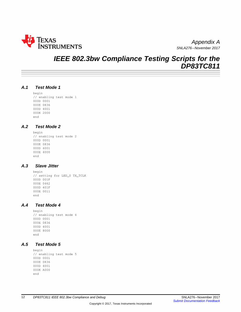
IEEE 802.3bw Compliance Testing Scripts for theDP83TC811
A.1 Test Mode 1begin// enabling test mode 1000D 0001000E 0836000D 4001000E 2000end
A.2 Test Mode 2begin// enabling test mode 2000D 0001000E 0836000D 4001000E 4000end
A.3 Slave Jitterbegin// setting for LED_0 TX_TCLK000D 001F000E 0462000D 401F000E 0011end
A.4 Test Mode 4begin// enabling test mode 4000D 0001000E 0836000D 4001000E 8000end
A.5 Test Mode 5begin// enabling test mode 5000D 0001000E 0836000D 4001000E A000end

13SNLA276–November 2017Submit Documentation Feedback
Copyright © 2017, Texas Instruments Incorporated
DP83TC811 IEEE 802.3bw Compliance and Debug
Appendix BSNLA276–November 2017
Loopback and BIST Mode Scripts for the DP83TC811
B.1 xMII Loopbackbegin0000 6100 //enables xMII Loopbackend
B.2 Reverse Loopbackbegin0016 0110 //enables reverse loopback modeend
B.3 BIST Scriptbegin001B 007D //bits[7:0] determine IPG, default 0x7D is equal to 500 bytes (125 * 4 bytes)001C 05EE //bits[10:0] determine packet length, default 0x5EE is equal to 1514 bytes0016 7100 //enable continuous error check BIST modeend
B.4 BIST With Reverse Loopbackbegin001B 007D //bits[7:0] determine IPG, default 0x7D is equal to 500 bytes (125 * 4 bytes)001C 05EE //bits[10:0] determine packet length, default 0x5EE is equal to 1514 bytes0016 7110 //enable continuous error check BIST mode with reverse loopback modeend
B.5 BIST Status and Error Countbegin0016 //reads address 0x0016, bits[11:9] show packet generator and checker status001B 807D //writes bit[15] to ‘1’, sets bits[7:0] for 500 bytes (125 * 4 bytes) IPG001B //reads address 0x001B, bits[15:8] show BIST Error Countend

14 SNLA276–November 2017Submit Documentation Feedback
Copyright © 2017, Texas Instruments Incorporated
DP83TC811 IEEE 802.3bw Compliance and Debug
Appendix CSNLA276–November 2017
PHY Test Mode Waveforms
C.1 Transmitter Output DroopFigure 4 and Figure 5 show graphs of the transmitter output positive and negative droop, respectively.
Figure 4. Transmitter Output Droop (Positive)
Figure 5. Transmitter Output Droop (Negative)

www.ti.com Transmitter Output Droop
15SNLA276–November 2017Submit Documentation Feedback
Copyright © 2017, Texas Instruments Incorporated
DP83TC811 IEEE 802.3bw Compliance and Debug
Figure 6 shows a graph of the transmitter distortion.
Figure 6. Transmitter Distortion
Figure 7 shows a graph of the PSD mask.
Figure 7. PSD Mask

Frequency (MHz)
dB
0 20 40 60 80 100 120 140 160 180 200-70
-65
-60
-55
-50
-45
-40
-35
D001
LimitData
Frequency (MHz)
dB
0 10 20 30 40 50 60 70-30
-25
-20
-15
-10
D002
LimitData
Transmitter Output Droop www.ti.com
16 SNLA276–November 2017Submit Documentation Feedback
Copyright © 2017, Texas Instruments Incorporated
DP83TC811 IEEE 802.3bw Compliance and Debug
Figure 8 shows a graph of the MDI return loss.
Figure 8. MDI Return Loss
Figure 9 shows a graph of the MDI mode conversion.
Figure 9. MDI Mode Conversion
www.ti.com Transmitter Output Droop
17SNLA276–November 2017Submit Documentation Feedback
Copyright © 2017, Texas Instruments Incorporated
DP83TC811 IEEE 802.3bw Compliance and Debug
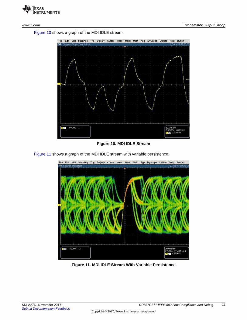
Figure 10 shows a graph of the MDI IDLE stream.
Figure 10. MDI IDLE Stream
Figure 11 shows a graph of the MDI IDLE stream with variable persistence.
Figure 11. MDI IDLE Stream With Variable Persistence

IMPORTANT NOTICE FOR TI DESIGN INFORMATION AND RESOURCES
Texas Instruments Incorporated (‘TI”) technical, application or other design advice, services or information, including, but not limited to,reference designs and materials relating to evaluation modules, (collectively, “TI Resources”) are intended to assist designers who aredeveloping applications that incorporate TI products; by downloading, accessing or using any particular TI Resource in any way, you(individually or, if you are acting on behalf of a company, your company) agree to use it solely for this purpose and subject to the terms ofthis Notice.TI’s provision of TI Resources does not expand or otherwise alter TI’s applicable published warranties or warranty disclaimers for TIproducts, and no additional obligations or liabilities arise from TI providing such TI Resources. TI reserves the right to make corrections,enhancements, improvements and other changes to its TI Resources.You understand and agree that you remain responsible for using your independent analysis, evaluation and judgment in designing yourapplications and that you have full and exclusive responsibility to assure the safety of your applications and compliance of your applications(and of all TI products used in or for your applications) with all applicable regulations, laws and other applicable requirements. Yourepresent that, with respect to your applications, you have all the necessary expertise to create and implement safeguards that (1)anticipate dangerous consequences of failures, (2) monitor failures and their consequences, and (3) lessen the likelihood of failures thatmight cause harm and take appropriate actions. You agree that prior to using or distributing any applications that include TI products, youwill thoroughly test such applications and the functionality of such TI products as used in such applications. TI has not conducted anytesting other than that specifically described in the published documentation for a particular TI Resource.You are authorized to use, copy and modify any individual TI Resource only in connection with the development of applications that includethe TI product(s) identified in such TI Resource. NO OTHER LICENSE, EXPRESS OR IMPLIED, BY ESTOPPEL OR OTHERWISE TOANY OTHER TI INTELLECTUAL PROPERTY RIGHT, AND NO LICENSE TO ANY TECHNOLOGY OR INTELLECTUAL PROPERTYRIGHT OF TI OR ANY THIRD PARTY IS GRANTED HEREIN, including but not limited to any patent right, copyright, mask work right, orother intellectual property right relating to any combination, machine, or process in which TI products or services are used. Informationregarding or referencing third-party products or services does not constitute a license to use such products or services, or a warranty orendorsement thereof. Use of TI Resources may require a license from a third party under the patents or other intellectual property of thethird party, or a license from TI under the patents or other intellectual property of TI.TI RESOURCES ARE PROVIDED “AS IS” AND WITH ALL FAULTS. TI DISCLAIMS ALL OTHER WARRANTIES ORREPRESENTATIONS, EXPRESS OR IMPLIED, REGARDING TI RESOURCES OR USE THEREOF, INCLUDING BUT NOT LIMITED TOACCURACY OR COMPLETENESS, TITLE, ANY EPIDEMIC FAILURE WARRANTY AND ANY IMPLIED WARRANTIES OFMERCHANTABILITY, FITNESS FOR A PARTICULAR PURPOSE, AND NON-INFRINGEMENT OF ANY THIRD PARTY INTELLECTUALPROPERTY RIGHTS.TI SHALL NOT BE LIABLE FOR AND SHALL NOT DEFEND OR INDEMNIFY YOU AGAINST ANY CLAIM, INCLUDING BUT NOTLIMITED TO ANY INFRINGEMENT CLAIM THAT RELATES TO OR IS BASED ON ANY COMBINATION OF PRODUCTS EVEN IFDESCRIBED IN TI RESOURCES OR OTHERWISE. IN NO EVENT SHALL TI BE LIABLE FOR ANY ACTUAL, DIRECT, SPECIAL,COLLATERAL, INDIRECT, PUNITIVE, INCIDENTAL, CONSEQUENTIAL OR EXEMPLARY DAMAGES IN CONNECTION WITH ORARISING OUT OF TI RESOURCES OR USE THEREOF, AND REGARDLESS OF WHETHER TI HAS BEEN ADVISED OF THEPOSSIBILITY OF SUCH DAMAGES.You agree to fully indemnify TI and its representatives against any damages, costs, losses, and/or liabilities arising out of your non-compliance with the terms and provisions of this Notice.This Notice applies to TI Resources. Additional terms apply to the use and purchase of certain types of materials, TI products and services.These include; without limitation, TI’s standard terms for semiconductor products http://www.ti.com/sc/docs/stdterms.htm), evaluationmodules, and samples (http://www.ti.com/sc/docs/sampterms.htm).
Mailing Address: Texas Instruments, Post Office Box 655303, Dallas, Texas 75265Copyright © 2017, Texas Instruments Incorporated