DP83843 PHYTER (Rev. B) - TI.com
89
DP83843 DP83843 PHYTER
Transcript of DP83843 PHYTER (Rev. B) - TI.com

DP83843
DP83843 PHYTER
Literature Number: SNLS021B

DP
83843BV
JE P
HY
TE
R
© 1999 National Semiconductor Corporationwww.national.com
Nov 2013
DP83843BVJE PHYTER
General DescriptionThe DP83843BVJE is a full feature Physical Layer devicewith integrated PMD sublayers to support both 10BASE-Tand 100BASE-X Ethernet protocols.This VLSI device is designed for easy implementation of10/100 Mb/s Ethernet LANs. It interfaces directly to TwistedPair media through an external transformer or to fibermedia via industry standard electrical/optical fiber PMDtransceivers. This device also interfaces directly to theMAC layer through the IEEE 802.3u standard Media Inde-pendent Interface (MII), ensuring interoperability betweenproducts from different vendors.The DP83843 is designed with National Semiconductor'sadvanced CMOS process. Its system architecture is basedon the integration of several of National's industry provencore technologies:— IEEE 802.3 ENDEC with AUI/10BASE-T transceiver
module to provide the 10 Mb/s functions— Clock Recovery/Generator Modules from National's Fast
Ethernet and FDDI products— FDDI Stream Cipher scrambler/descrambler for
TP-PMD— 100BASE-X physical coding sub-layer (PCS) and control
logic that integrates the core modules into a dual speedEthernet physical layer controller
— ANSI X3T12 Compliant TP-PMD Transceivertechnology with Baseline Wander (BLW) compensation
System Diagram
ThunderLAN® is a registered trademark of Texas Instruments.TWISTER™ is a trademark of National Semiconductor Corporation.TRI-STATE® is a registered trademark of National Semiconductor Corporation.
10 AND/OR 100 Mb/sETHERNET MAC OR100Mb/s REPEATER
DP8384310/100 Mb/s
ETHERNET PHYSICAL LAYER
STATUSLEDS
MAG
NE
TIC
S
RJ-4510BASE-T
or100BASE-TX
MII
10BASE-T or
CONTROLLER
100BASE-TX
100BASE-FX/
CLOCK25 MHz
AUI
Features— IEEE 802.3 ENDEC with AUI/10BASE-T transceivers
and built-in filters— IEEE 802.3u 100BASE-TX compatible - directly drives
standard Category 5 UTP, no need for external100BASE-TX transceiver
— Fully Integrated and fully compliant ANSI X3.263 TP-PMD physical sublayer which includes adaptive equal-ization and BLW compensation
— IEEE 802.3u 100BASE-FX compatible - connects direct-ly to industry standard Electrical/Optical transceivers
— IEEE 802.3u Auto-Negotiation for automatic speed se-lection
— IEEE 802.3u compatible Media Independent Interface(MII) with Serial Management Interface
— Integrated high performance 100 Mb/s clock recoverycircuitry requiring no external filters
— Full Duplex support for 10 and 100 Mb/s data rates— MII Serial 10 Mb/s mode— Fully configurable node/switch and 100Mb/s repeater
modes— Programmable loopback modes for flexible system diag-
nostics— Flexible LED support— Single register access to complete PHY status— MDIO interrupt support— Individualized scrambler seed for 100BASE-TX applica-
tions using multiple PHYs— Low power consumption for multi-port applications— Small footprint 80-pin PQFP package

2 www.national.com
Block Diagram
SERIALMANAGEMENT
MII
TX
_CLK
TX
D[3
:0]
TX
_ER
TX
_EN
MD
IO
MD
C
CO
L
CR
S
RX
_ER
RX
_DV
RX
D[3
:0]
RX
_CL
MII INTERFACE/CONTROL
RX
_EN
TRANSMIT CHANNELS &
100 MB/S 10 MB/S
NRZ TO MANCHESTER
ENCODER
STATE MACHINES
TRANSMITFILTER
LINK PULSEGENERATOR
4B/5BENCODER
SCRAMBLER
PARALLEL TOSERIAL
NRZ TO NRZIENCODER
BINARY TOMLT-3
ENCODER
10/100 COMMON
RECEIVE CHANNELS &
100 MB/S 10 MB/S
MANCHESTERTO NRZ
DECODER
STATE MACHINES
RECEIVEFILTER
LINK PULSEDETECTOR
4B/5BDECODER
DESCRAMBLER
SERIAL TOPARALLEL
NRZI TO NRZDECODER
MLT-3 TO
10/100 COMMON
AUTO-NEGOTIATIONSTATE MACHINE
FAR-END-FAULTSTATE MACHINE
REGISTERS
AUTO
100BASE-X
10BASE-T
MII
NODE/RPTR
PCS CONTROL
PHY ADDRESS
NEGOTIATION
CLOCK
CLOCKRECOVERY
CLOCKRECOVERY
CODE GROUPALIGNMENT
SMARTSQUELCH
RX_DATA
RX_CLK
RX_DATARX_CLK
TX_DATA TX_DATA TX_CLK
SYSTEM CLOCKREFERENCE
FXSD/CD+/−
TPRD+/−TPTD+/−
OUTPUT DRIVER
FXTD/AUITD+/−
INPUT BUFFER
BINARYDECODER
ADAPTIVEEQANDBLW
COMP.
FXRD/AUIRD+/−
LEDDRIVERS
LEDS
HARDWARECONFIGURATION
PINS
TXAR100
(REPEATER,SERIAL10, SYMBOL,
AN0, AN1,FXEN PHYAD[4:0])
,
GENERATION

3 www.national.com
Table of Contents1.0 Pin Descriptions . . . . . . . . . . . . . . . . . . . . . . . . . . . . . . . 5
1.1 MII Interface . . . . . . . . . . . . . . . . . . . . . . . . . . . . . . 51.2 10 Mb/s and 100 Mb/s PMD Interface . . . . . . . . . . 61.3 Clock Interface . . . . . . . . . . . . . . . . . . . . . . . . . . . . 81.4 Device Configuration Interface . . . . . . . . . . . . . . . 81.5 LED Interface . . . . . . . . . . . . . . . . . . . . . . . . . . . . 101.6 PHY Address Interface . . . . . . . . . . . . . . . . . . . . 111.7 Reset . . . . . . . . . . . . . . . . . . . . . . . . . . . . . . . . . . 111.8 Power And Ground Pins . . . . . . . . . . . . . . . . . . . 121.9 Special Connect Pins . . . . . . . . . . . . . . . . . . . . . . 12
2.0 Functional Description . . . . . . . . . . . . . . . . . . . . . . . . . 132.1 802.3u MII . . . . . . . . . . . . . . . . . . . . . . . . . . . . . . 132.2 100BASE-TX TRANSMITTER . . . . . . . . . . . . . . . 152.3 100BASE-TX RECEIVER . . . . . . . . . . . . . . . . . . 182.4 10BASE-T TRANSCEIVER MODULE . . . . . . . . . 222.5 100 BASE-FX . . . . . . . . . . . . . . . . . . . . . . . . . . . 242.6 AUI . . . . . . . . . . . . . . . . . . . . . . . . . . . . . . . . . . . . 26
3.0 Configuration . . . . . . . . . . . . . . . . . . . . . . . . . . . . . . . . 283.1 Auto-Negotiation . . . . . . . . . . . . . . . . . . . . . . . . . 283.2 PHY Address and LEDs . . . . . . . . . . . . . . . . . . . 303.3 Half Duplex vs. Full Duplex . . . . . . . . . . . . . . . . . 313.4 100 Mb/s Symbol Mode . . . . . . . . . . . . . . . . . . . . 323.5 100BASE-FX Mode . . . . . . . . . . . . . . . . . . . . . . . 323.6 10 Mb/s Serial Mode . . . . . . . . . . . . . . . . . . . . . . 323.7 10 Mb/s AUI Mode . . . . . . . . . . . . . . . . . . . . . . . . 323.8 Repeater vs. Node . . . . . . . . . . . . . . . . . . . . . . . . 333.9 Isolate Mode . . . . . . . . . . . . . . . . . . . . . . . . . . . . 333.10 Loopback . . . . . . . . . . . . . . . . . . . . . . . . . . . . . . . 33
4.0 Clock Architecture . . . . . . . . . . . . . . . . . . . . . . . . . . . . 344.1 Clock Generation Module (CGM) . . . . . . . . . . . . 344.2 100BASE-X Clock Recovery Module . . . . . . . . . . 364.3 10 Mb/s Clock Recovery Module . . . . . . . . . . . . . 364.4 Reference Clock Connection Options . . . . . . . . . 36
5.0 Reset Operation . . . . . . . . . . . . . . . . . . . . . . . . . . . . . . 375.1 Power-up / Reset . . . . . . . . . . . . . . . . . . . . . . . . . 375.2 Hardware Reset . . . . . . . . . . . . . . . . . . . . . . . . . . 375.3 Software Reset . . . . . . . . . . . . . . . . . . . . . . . . . . 37
6.0 DP83843 Application . . . . . . . . . . . . . . . . . . . . . . . . . . 386.1 Typical Node Application . . . . . . . . . . . . . . . . . . . 386.2 Power And Ground Filtering . . . . . . . . . . . . . . . . 386.3 Power Plane Considerations . . . . . . . . . . . . . . . . 38
7.0 User Information . . . . . . . . . . . . . . . . . . . . . . . . . . . . . 427.1 Link LED While in Force 100Mb/s Good Link . . . 427.2 False Link Indication When in Forced 10Mb/s . . 427.3 10Mb/s Repeater Mode . . . . . . . . . . . . . . . . . . . 427.4 Resistor Value Modifications . . . . . . . . . . . . . . . 427.5 Magnetics . . . . . . . . . . . . . . . . . . . . . . . . . . . . . . 437.6 Next Page Toggle Bit Initialization . . . . . . . . . . . 437.7 Base Page to Next Page Initial FLP Burst Spacing
437.8 100Mb/s FLP Exchange Followed by Quiet . . . . 437.9 Common Mode Capacitor for EMI improvement 447.10 BAD_SSD Event Lockup . . . . . . . . . . . . . . . . . . 44
8.0 Register Block . . . . . . . . . . . . . . . . . . . . . . . . . . . . . . . 458.1 Register Definitions . . . . . . . . . . . . . . . . . . . . . . 45
9.0 Electrical Specifications . . . . . . . . . . . . . . . . . . . . . . . 639.1 DC Electrical Specification . . . . . . . . . . . . . . . . . 649.2 CGM Clock Timing . . . . . . . . . . . . . . . . . . . . . . 669.3 MII Serial Management AC Timing . . . . . . . . . . 669.4 100 Mb/s AC Timing . . . . . . . . . . . . . . . . . . . . . . 679.5 10 Mb/s AC Timing . . . . . . . . . . . . . . . . . . . . . . . 749.6 Auto-Negotiation Fast Link Pulse (FLP) Timing 809.7 100BASE-X Clock Recovery Module (CRM) Timing
809.8 Reset Timing . . . . . . . . . . . . . . . . . . . . . . . . . . 829.9 Loopback Timing . . . . . . . . . . . . . . . . . . . . . . . 839.10 Isolation Timing . . . . . . . . . . . . . . . . . . . . . . . . 84
10.0 Test Conditions . . . . . . . . . . . . . . . . . . . . . . . . . . . . . . 8510.1 FXTD/AUITD+/- Outputs (sourcing AUI levels) . 8510.2 FXTD/AUITD+/- Outputs (sourcing PECL) . . . . . 8510.3 CMOS Outputs (MII and LED) . . . . . . . . . . . . . . 8510.4 TPTD+/- Outputs (sourcing 10BASE-T) . . . . . . . 8510.5 TPTD+/- Outputs (sourcing 100BASE-TX) . . . . . 8510.6 Idd Measurement Conditions . . . . . . . . . . . . . . . 85
11.0 Package Dimensions inches (millimeters) unless other-wise noted . . . . . . . . . . . . . . . . . . . . . . . . . . . . . . . . . . 87

4 www.national.com
Connection Diagram
LED_RX/PHYAD[2]LED_LINK/PHYAD[3]LED_FDPOL/PHYAD[4]
MDC
IO_VSS3IO_VDD3
CRS/SYMBOLRX_ENTX_ERTX_EN
MDIOTX_CLK
IO_VSS5IO_VDD5
TXD[0]TXD[1]TXD[2]TXD[3]
COL/FXEN
IO_VSS4
CD_GND1
CD_VDD0
TPTD+TPTD-
SUB_GND2
TR_AGND
TW_AGND
TW_AVDD
TR_AVDD
TPRD-
SUB_GND1
TXAR100
TPRD+
CD_GND0
NCTHIN/REPEATER
SERIAL10
CD_VDD1
VCM_CAP
BGREF
RX
D[2
]R
XD
[3]
RE
SE
T
PC
S_V
SS
PC
S_V
DD
AN
1A
N0
SP
EE
D10 X2
X1
IO_V
DD
1
IO_V
DD
2IO
_VS
S2
IO_V
SS
1
NC
RX
D[0
]R
XD
[1]
RX
_DV
RX
_ER
RX
_CLK
TWR
EF
CP
TW_D
VS
SC
PTW
_DV
DD
NC
CP
_AV
DD
FXS
D+/
CD
+FX
SD
-/CD
-
CP
_AG
ND
AUIF
X_V
DD
AUIF
X_G
ND
NC
FXTD
+/AU
ITD
+
FXR
D-/A
UIR
D-
FXR
D+/
AUIR
D+
FXTD
-/AU
ITD
-
NC
NC
ATP
_GN
D
LED
_TX
/PH
YAD
[1]
LED
_CO
L/P
HYA
D[0
]
6162636465666768697071727374757677787980
4039383736353433323130292827262524232221
1 2 3 4 5 6 7 8 9 10 11 12 13 14 15 16 17 18 19 20
60 59 58 57 56 55 54 53 52 51 50 49 48 47 46 45 44 43 42 41
DP83843BVJEPHYTER
Order Number DP83843BVJENS Package Number VJE80

5 www.national.com
1.0 Pin Descriptions
The DP83843 pins are classified into the following interfacecategories. Each interface is described in the sections thatfollow.— MII INTERFACE— 10/100 Mb/s PMD INTERFACE— CLOCK INTERFACE
— DEVICE CONFIGURATION INTERFACE— LED INTERFACE— PHY ADDRESS INTERFACE— RESET— POWER AND GROUND PINS— SPECIAL CONNECT PINS
1.1 MII Interface
Signal Name Type Pin # Description
MDC I 35 MANAGEMENT DATA CLOCK: Synchronous clock to the MDIO management data in-put/output serial interface which may be asynchronous to transmit and receive clocks.The maximum clock rate is 2.5 MHz. There is no minimum clock rate.
MDIO I/O, Z 34 MANAGEMENT DATA I/O: Bi-directional management instruction/data signal that maybe sourced by the station management entity or the PHY. This pin requires a 1.5 kΩ pul-lup resistor.
CRS(SYMBOL)
I/O, Z 22 CARRIER SENSE: This pin is asserted high to indicate the presence of carrier due toreceive or transmit activities in 10BASE-T or 100BASE-X Half Duplex modes.In Repeater or Full Duplex mode, this pin is asserted high to indicate the presence ofcarrier due only to receive activity.In Symbol mode this pin indicates the signal detect status of the TP-PMD (active high).
COL(FXEN)
I/O, Z 21 COLLISION DETECT: Asserted high to indicate detection of collision condition (asser-tion of CRS due to simultaneous transmit and receive activity) in 10 Mb/s and 100 Mb/sHalf Duplex modes.While in 10BASE-T Half Duplex mode with Heartbeat enabled (bit 7, register 18h), thispin is also asserted for a duration of approximately 1 µs at the end of transmission toindicate heartbeat (SQE test). During Repeater mode the heartbeat function is disabled.In Full Duplex mode, for 10 Mb/s or 100 Mb/s operation, this signal is always logic 0.There is no heartbeat function during 10 Mb/s full duplex operation.
TX_CLK O, Z 33 TRANSMIT CLOCK: Transmit clock output from the DP83843:25 MHz nibble transmit clock derived from Clock Generator Module's (CGM) PLL in100BASE-TX mode.2.5 MHz transmit clock in 10BASE-T Nibble mode.10 MHz transmit clock in 10BASE-T Serial mode.
TXD[3]TXD[2]TXD[1]TXD[0]
I 28293031
TRANSMIT DATA: Transmit data MII input pins that accept nibble data during normalnibble-wide MII operation at either 2.5 MHz (10BASE-T mode) or 25 MHz (100BASE-Xmode).In 10 Mb/s Serial mode, the TXD[0] pin is used as the serial data input pin, and TXD[3:1]are ignored.
TX_EN I 25 TRANSMIT ENABLE: Active high input indicates the presence of valid nibble data onTXD[3:0] for both 100 Mb/s or 10 Mb/s nibble mode.In 10 Mb/s Serial mode, active high indicates the presence of valid 10 Mb/s data onTXD[0].
TX_ER(TXD[4])
I 24 TRANSMIT ERROR: In 100 Mb/s mode, when this signal is high and TX_EN is activethe HALT symbol is substituted for the actual data nibble.In 10 Mb/s mode, this input is ignored.In Symbol mode (Symbol=0), TX_ER becomes the TXD [4] pin which is the MSB for thetransmit 5-bit data symbol.
RX_CLK O, Z 18 RECEIVE CLOCK: Provides the recovered receive clock for different modes of opera-tion:25 MHz nibble clock in 100 Mb/s mode2.5 MHz nibble clock in 10 Mb/s nibble mode10 MHz receive clock in 10 Mb/s serial mode

1.0 Pin Descriptions (Continued)
6 www.national.com
1.2 10 Mb/s and 100 Mb/s PMD Interface
RXD[3]RXD[2]RXD[1]RXD[0]
O, Z 12131415
RECEIVE DATA: Nibble wide receive data (synchronous to RX_CLK, 25 MHz for100BASE-X mode, 2.5 MHz for 10BASE-T nibble mode). Data is driven on the fallingedge of RX_CLK.In 10 Mb/s serial mode, the RXD[0] pin is used as the data output pin which is alsoclocked out on the falling edge of RX_CLK. During 10 Mb/s serial mode RXD[3:1] pinsbecome don't cares.
RX_EN I 23 RECEIVE ENABLE: Active high enable for receive signals RXD[3:0], RX_CLK, RX_DVand RX_ER. A low on this input places these output pins in the TRI-STATE mode. Fornormal operation in a node or switch application, this pin should be pulled high. For op-eration in a repeater application, this pin may be connected to a repeater controller.
RX_ER(RXD[4])
O, Z 19 RECEIVE ERROR: Asserted high to indicate that an invalid symbol has been detectedwithin a received packet in 100 Mb/s mode.In Symbol mode (Symbol = 0), RX_ER becomes RXD[4] which is the MSB for the re-ceive 5-bit data symbol.
RX_DV O, Z 20 RECEIVE DATA VALID: Asserted high to indicate that valid data is present on RXD[3:0]for nibble mode and RXD[0] for serial mode. Data is driven on the falling edge ofRX_CLK.This pin is not meaningful during Symbol mode.
Signal Name Type Pin # Description
Signal Name Type Pin # Description
TPTD-TPTD+
O(MLT-3or10BASE-T)
7374
TRANSMIT DATA: Differential common output driver. This differential outputis configurable to either 10BASE-T or 100BASE-TX signaling:10BASE-T: Transmission of Manchester encoded 10BASE-T packet data aswell as Link Pulses (including Fast Link Pulses for Auto-Negotiation purpos-es.)100BASE-TX: Transmission of ANSI X3T12 compliant MLT-3 data.The DP83843 will automatically configure this common output driver for theproper signal type as a result of either forced configuration or Auto-Negotia-tion.
TPRD-TPRD+
I(MLT-3or10BASE-T)
6567
RECEIVE DATA: Differential common input buffer. This differential input canbe configured to accept either 100BASE-TX or 10BASE-T signaling:10BASE-T: Reception of Manchester encoded 10BASE-T packet data as wellas normal Link Pulses (including Fast Link Pulses for Auto-Negotiation pur-poses.)100BASE-TX: Reception of ANSI X3T12 compliant scrambled MLT-3 data.The DP83843 will automatically configure this common input buffer to acceptthe proper signal type as a result of either forced configuration or Auto-Nego-tiation.
FXTD-/AUITD-FXTD+/AUITD+
O(PECLorAUI)
4443
100BASE-FX or 10 Mb/s AUI TRANSMIT DATA: This configurable outputdriver supports either 125 Mb/s PECL, for 100BASE-FX applications, or10 Mb/s AUI signaling.When configured as a 100BASE-FX transmitter this output sources100BASE-FX standard compliant binary data for direct connection to an opti-cal transceiver. This differential output is enabled only during 100BASE-FXdevice configuration (see pin definition for FXEN.)When configured as an AUI driver this output sources AUI compatibleManchester encoded data to support typical 10BASE2 or 10BASE5 products.

1.0 Pin Descriptions (Continued)
7 www.national.com
FXRD-/AUIRD-FXRD+/AUIRD+
I(PECLorAUI)
4950
100BASE-FX or 10 Mb/s AUI RECEIVE DATA: This configurable input buff-er supports either 125 Mb/s PECL, for 100BASE-FX applications, or 10 Mb/sAUI signaling.When configured as a 100BASE-FX receiver this input accepts 100BASE-FXstandard compliant binary data direct from an optical transceiver. This differ-ential input is enabled only during 100BASE-FX device configuration (see thepin definition for FXEN).When configured as an AUI buffer this input receives AUI compatibleManchester data to support typical 10BASE2 or 10BASE5 products.
FXSD-/CD-FXSD+/CD+
I(PECLorAUI)
4748
SIGNAL DETECT or AUI COLLISION DETECT: This configurable input buff-er supports either 125 Mb/s PECL, for 100BASE-FX applications, or 10 Mb/sAUI signaling.When configured as a 100BASE-FX receiver this input accepts indicationfrom the 100BASE-FX PMD transceiver upon detection of a receive signalfrom the fiber media. This pin is only active during 100BASE-FX opera-tion(see the pin definition for FXEN).When configured as an AUI buffer this input receives AUI compatibleManchester data to support typical 10BASE2 or 10BASE5 products.
THIN(REPEATER)
I/O, Z 63 THIN AUI MODE: This output allows for control of an external CTI coaxialtransceiver connected through the AUI. This pin is controlled by writing to bit3 of the 10BTSCR register (address 18h). The THIN pin may also be used asa user configurable output control pin.
TXAR100 I(currentreference)
78 100 Mb/s TRANSMIT AMPLITUDE REFERENCE CONTROL: Referencecurrent allowing adjustment of the TPTD+/− output amplitude during100BASE-TX operation.By placing a resistor between this pin and ground or VCC, a reference currentis set up which dictates the output amplitude of the 100BASE-TX MLT-3transmit signal. Connecting a resistor to VCC will increase the transmit ampli-tude while connecting a resistor to ground will decrease the transmit ampli-tude. While the value of the resistor should be evaluated on a case by casebases, the DP83843 was designed to produce an amplitude close to the re-quired range of 2V pk-pk differential ± 5% as measured across TD+/− whiledriving a typical 100Ω differential load without a resistor connected to this pin.Therefore this pin is allowed to float in typical applications.This current reference is only recognized during 100BASE-TX operation andhas no effect during100BASE-FX,10BASE-T, or AUI modes of operation.
TWREF I 60 TWISTER REFERENCE RESISTOR: External reference current adjustment,via a resistor to TW_AGND, which controls the TP-PMD receiver equalizationlevels. The value of this resistor is 70k ± 1%.
BGREF I(currentreference)
61 BANDGAP REFERENCE: External current reference resistor for internalbandgap circuitry. The value of this resistor is 4.87k ± 1%.
VCM_CAP I 66 COMMON MODE BYPASS CAPACITOR: External capacitor to improvecommon mode filtering for the receive signal. It is recommended that a.0033µF in parallel with a .10µF capacitor be used, see Figure 23.
Signal Name Type Pin # Description

1.0 Pin Descriptions (Continued)
8 www.national.com
1.3 Clock Interface
1.4 Device Configuration Interface
Signal Name Type Pin # Description
X1 I 9 CRYSTAL/OSCILLATOR INPUT: This pin is the primary clock reference input forthe DP83843 and must be connected to a 25 MHz 0.005% (50 ppm) clock source.The DP83843 device supports either an external crystal resonator connected acrosspins X1 and X2, or an external CMOS-level oscillator source connected to pin X1only. For 100 Mb/s repeater applications, X1 should be tied to the common 25 MHztransmit clock reference. Refer to section 4.4 for further detail relating to the clockrequirements of the DP83843. Refer to section 4.0 for clock source specifications.
X2 O 8 CRYSTAL/OSCILLATOR OUTPUT PIN: This pin is used in conjunction with the X1pin to connect to an external 25 MHz crystal resonator device. This pin must be leftunconnected if an external CMOS oscillator clock source is utilized. For more infor-mation see the definition for pin X1. Refer to section 2.8 for further detail.
Signal Name Type Pin # Description
AN0 I(3-level)
4 AN0: This is a three level input pin (1, M, 0) that works in conjunction with the AN1pin to control the forced or advertised operating mode of the DP83843 according tothe following table. The value on this pin is set by connecting the input pin to GND(0), VCC (1), or leaving it unconnected (M.) The unconnected state, M, refers to themid-level (VCC/2) set by internal resistors. The value set at this input is latched intothe DP83843 at power-up/reset.
AN1 I(3-level)
3 AN1: This is a three-level input pin (i.e., 1, M, 0) that works in conjunction with theAN0 pin to control the forced or advertised operating mode of the DP83843 accord-ing to the table given in the AN0 pin description above. The value on this pin is setby connecting the input pin to GND (0), VCC (1), or leaving it unconnected (M.) Thevalue at this input is latched into the DP83843 at power-up, hardware or softwarereset.
AN1 AN0 Forced Mode0 M 10BASE-T, Half-Duplex without Auto-Negotiation1 M 10BASE-T, Full Duplex without Auto-NegotiationM 0 100BASE-X, Half-Duplex without Auto-NegotiationM 1 100BASE-X, Full Duplex without Auto-Negotiation
AN1 AN0 Advertised ModeM M All capable (i.e. Half-Duplex & Full Duplex for 10BASE-T and
100BASE-TX) advertised via Auto-Negotiation0 0 10BASE-T, Half-Duplex & Full Duplex advertised via Auto-
Negotiation0 1 100BASE-TX, Half-Duplex & Full Duplex advertised via
Auto-Negotiation1 0 10BASE-T & 100BASE-TX, Half-Duplex advertised via Auto-
Negotiation1 1 10 BASE-T, Half-Duplex advertised via Auto-Negotiation

1.0 Pin Descriptions (Continued)
9 www.national.com
REPEATER(THIN)
I/O 63 REPEATER/NODE MODE: Selects 100 Mb/s Repeater mode when set high andnode mode when set low. When set in Repeater mode the DP83843 only supports100 Mb/s data rates. In Repeater mode (or Node mode with Full Duplex config-ured), the Carrier Sense (CRS) output from the DP83843 is asserted due toreceive activity only. In Half Duplex Node mode, CRS is asserted due to eitherreceive or transmit activity. During repeater mode the heartbeat function(SQE) isforced off.The Carrier Integrity Monitor (CIM) function is automatically enabled when this pinis set high (repeater mode) and disabled when this pin is set low (node mode) inorder to facilitate 802.3u CIM requirements.There is an internal pullup resistor for this pin which is active during the power-up/reset period. If this pin is left floating externally, then the device will configure to100 Mb/s Repeater mode as a result of power-up/reset. This pin must be externallypulled low (typically 10 kΩ) in order to configure the DP83843 for Node operation.The value of this input is latched into the DP83843 at power-up, hardware or soft-ware reset.
SYMBOL/(CRS)
I/O, Z 22 SYMBOL MODE: This active low input allows 100 Mb/s transmit and receive datastreams to bypass all of the transmit and receive operations when set low. Notethat the PCS signals (CRS, RX_DV, RX_ER, and COL) have no meaning duringthis mode. During Symbol operation, pins RX_ER/RXD[4] and TX_ER/TXD[4] areused as the MSB of the 5 bit RX and TX data symbols.There is an internal pullup resistor for this pin which is active during the power-up/reset period. If this pin is left floating externally, then the device will configure tonormal mode as a result of power-up/reset. This pin must be externally pulled low(typically 10 kΩ) in order to configure the DP83843 for Symbol mode operation.In Symbol mode this pin will indicate the signal detect status of the TP-PMD (activehigh).This mode has no effect on 10Mb/s operation. The value at this input is latched intothe DP83843 at power-up, hardware or software reset.
SERIAL10 I 69 10BASE-T SERIAL/NIBBLE SELECT: With this active low input selected, transmitand receive data are exchanged serially at a 10 MHz clock rate on the least signifi-cant bits of the nibble-wide MII data buses, pins TXD[0] and RXD[0] respectively.This mode is intended for use with the DP83843 connected to a MAC using a 10Mb/s serial interface. Serial operation is not supported in 100 Mb/s mode, thereforethis input is ignored during 100 Mb/s operation.There is an internal pullup resistor for this pin which is active during the power-up/reset period. If this pin is left floating externally, then the device will configure tonormal mode as a result of power-up/reset. This pin must be externally pulled low(typically 10 kΩ) in order to configure the DP83843 for Serial MII operation whenrunning at 10 Mb/s.The value at this input is latched into the DP83843 at power-up, hardware or soft-ware reset.
FXEN/(COL)
I/O, Z 21 FIBER ENABLE: This active low input allows 100 Mb/s transmit and receive datastreams to bypass the scrambler and descrambler circuits when selected. All PCSsignaling remains active and unaffected during this mode. During this mode, theinternal 100 Mb/s transceiver is disabled, and NRZI data is transmitted andreceived via the FXTD/AUITD+/− and FXRD/AUIRD+/− pins.There is an internal pullup resistor for this pin which is active during the power-up/reset period. If this pin is left floating externally, then the device will configure tonormal mode as a result of power-up/reset. This pin must be externally pulled low(typically 10 kΩ) in order to configure the DP83843 for 100BASE-FX operation.The value at this input is latched into the DP83843 at power-up, hardware or soft-ware reset.
Signal Name Type Pin # Description
1.0 Pin Descriptions (Continued)
10 www.national.com
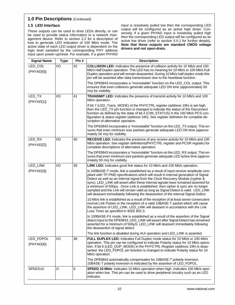
1.5 LED InterfaceThese outputs can be used to drive LEDs directly, or canbe used to provide status information to a network man-agement device. Refer to section 2.2 for a description ofhow to generate LED indication of 100 Mb/s mode. Theactive state of each LED output driver is dependent on thelogic level sampled by the corresponding PHY addressinput upon power-up/reset. For example, if a given PHYAD
input is resistively pulled low then the corresponding LEDoutput will be configured as an active high driver. Con-versely, if a given PHYAD input is resistively pulled highthen the corresponding LED output will be configured as anactive low driver (refer to section 5.0.1 for further details).Note that these outputs are standard CMOS voltagedrivers and not open-drain.
Signal Name Type Pin # Description
LED_COL(PHYAD[0])
I/O 42 COLLISION LED: Indicates the presence of collision activity for 10 Mb/s and 100Mb/s Half Duplex operation. This LED has no meaning for 10 Mb/s or 100 Mb/s FullDuplex operation and will remain deasserted. During 10 Mb/s half duplex mode thispin will be asserted after data transmission due to the heartbeat function.The DP83843 incorporates a “monostable” function on the LED_COL output. Thisensures that even collisions generate adequate LED ON time (approximately 50ms) for visibility.
LED_TX(PHYAD[1])
I/O 41 TRANSMIT LED: Indicates the presence of transmit activity for 10 Mb/s and 100Mb/s operation.If bit 7 (LED_Trans_MODE) of the PHYCTRL register (address 19h) is set high,then the LED_TX pin function is changed to indicate the status of the Disconnectfunction as defined by the state of bit 4 (CIM_STATUS) in the 100 Mb/s PCS con-figuration & status register (address 16h). See register definition for complete de-scription of alternative operation.The DP83843 incorporates a “monostable” function on the LED_TX output. This en-sures that even minimum size packets generate adequate LED ON time (approxi-mately 50 ms) for visibility.
LED_RX(PHYAD[2])
I/O 40 RECEIVE LED: Indicates the presence of any receive activity for 10 Mb/s and 100Mb/s operation. See register definitions(PHYCTRL register and PCSR register) forcomplete descriptions of alternative operation.The DP83843 incorporates a “monostable” function on the LED_RX output. This en-sures that even minimum size packets generate adequate LED active time (approx-imately 50 ms) for visibility.
LED_LINK(PHYAD[3])
I/O 39 LINK LED: Indicates good link status for 10 Mb/s and 100 Mb/s operation.In 100BASE-T mode, link is established as a result of input receive amplitude com-pliant with TP-PMD specifications which will result in internal generation of SignalDetect as well as an internal signal from the Clock Recovery Module (cypher &sync). LED_LINK will assert after these internal signals have remained asserted fora minimum of 500µs. Once Link is established, then cipher & sync are no longersampled and the Link will remain valid as long as Signal Detect is valid. LED_LINKwill deassert immediately following the deassertion of the internal Signal Detect.10 Mb/s link is established as a result of the reception of at least seven consecutivenormal Link Pulses or the reception of a valid 10BASE-T packet which will causethe assertion of LED_LINK. LED_LINK will deassert in accordance with the LinkLoss Timer as specified in IEEE 802.3.In 100BASE-FX mode, link is established as a result of the assertion of the Signaldetect input to the DP83843. LED_LINK will assert after Signal Detect has remainedasserted for a minimum of 500µS. LED_LINK will deassert immediately followingthe deassertion of signal detect.The link function is disabled during AUI operation and LED_LINK is asserted.
LED_FDPOL(PHYAD[4])
I/O 38 FULL DUPLEX LED: Indicates Full Duplex mode status for 10 Mb/s or 100 Mb/soperation. This pin can be configured to indicate Polarity status for 10 Mb/s opera-tion. If bit 6 (LED_DUP_MODE) in the PHYCTRL Register (address 19h) is deas-serted, the LED_FDPOL pin function is changed to indicate Polarity status for 10Mb/s operation.The DP83843 automatically compensates for 10BASE-T polarity inversion.10BASE-T polarity inversion is indicated by the assertion of LED_FDPOL.
SPEED10 O 5 SPEED 10 Mb/s: Indicates 10 Mb/s operation when high. Indicates 100 Mb/s oper-ation when low. This pin can be used to drive peripheral circuitry such as an LEDindicator.

1.0 Pin Descriptions (Continued)
11 www.national.com
1.6 PHY Address InterfaceThe DP83843 PHYAD[4:0] inputs provide up to 32 uniquePHY address options. An address selection of all zeros
(00000) will result in a PHY isolation condition as aresult of power-on/reset, as specified in IEEE 802.3u.
1.7 Reset
Signal Name Type Pin # Description
PHYAD[0](LED_COL)
I/O 42 PHY ADDRESS [0]: PHY address sensing pin for multiple PHY applications. PHYaddress sensing is achieved by strapping a pull-up/pull-down resistor (typically 10kΩ) to this pin as required.The pull-up/pull-down status of this pin is latched into the PHYCTRL register (ad-dress 19h, bit 0) during power up/reset.
PHYAD[1](LED_TX)
I/O 41 PHY ADDRESS [1] : PHY address sensing pin for multiple PHY applications. PHYaddress sensing is achieved by strapping a pull-up/pull-down resistor (typically 10kΩ) to this pin as required.The pull-up/pull-down status of this pin is latched into the PHYCTRL register (ad-dress 19h, bit 1) during power up/reset.
PHYAD[2](LED_RX)
I/O 40 PHY ADDRESS [2]: PHY address sensing pin for multiple PHY applications. PHYaddress sensing is achieved by strapping a pull-up/pull-down resistor (typically 10kΩ) to this pin as required.The pull-up/pull-down status of this pin is latched into the PHYCTRL register (ad-dress 19h, bit 2) during power up/reset.
PHYAD[3](LED_LINK)
I/O 39 PHY ADDRESS [3]: PHY address sensing pin for multiple PHY applications. PHYaddress sensing is achieved by strapping a pull-up/pull-down resistor (typically 10kΩ) to this pin as required.The pull-up/pull-down status of this pin is latched into the PHYCTRL register (ad-dress 19h, bit 3) during power up/reset.
PHYAD[4](LED_FDPOL)
I/O 38 PHY ADDRESS [4]: PHY address sensing pin for multiple PHY applications. PHYaddress sensing is achieved by strapping a pull-up/pull-down resistor (typically 10kΩ) to this pin as required.The pull-up/pull-down status of this pin is latched into the PHYCTRL register (ad-dress 19h, bit 4) during power up/reset.
Signal Name Type Pin # Description
RESET I 1 RESET: Active high input that initializes or reinitializes the DP83843. Asserting thispin will force a reset process to occur which will result in all internal registers reini-tializing to their default states as specified for each bit in section 7.0, and all strap-ping options are reinitialized. Refer to section 5.0 for further detail regarding reset.

1.0 Pin Descriptions (Continued)
12 www.national.com
1.8 Power And Ground PinsThe power (VCC) and ground (GND) pins of the DP83843are grouped in pairs into three categories--TTL/CMOSInput pairs, Transmit/Receive supply pairs, and Internal
supply pairs. This grouping allows for optimizing the layoutand filtering of the power and ground supplies to thisdevice.
1.9 Special Connect Pins
Signal Name Pin # Description
TTL/CMOS INPUT/OUTPUT SUPPLY PAIRS
IO_VDD1IO_VSS1
67
TTL Input/Output Supply #1
IO_VDD2IO_VSS2
1617
TTL Input/Output Supply #2
IO_VDD3IO_VSS3
2627
TTL Input /Output Supply #3
IO_VSS4 32 TTL Input/Output Supply #4
IO_VDD5IO_VSS5
3637
TTL Input/ Output Supply #5
PCS_VDDPCS_VSS
1011
Physical Coding Sublayer Supply
TRANSMIT/RECEIVE SUPPLY PAIRS
AUIFX_VDDAUIFX_GND
4645
AUI Power Supply
TR_AVDDTR_AGND
7980
10 Mb/s Supply
TW_AVDDTW_AGND
6864
100 Mb/s Power Supply
CD_VDD0CD_GND0
7271
Common Driver Supply
CD_VDD1CD_GND1
7675
Common Driver Supply
INTERNAL SUPPLY PAIRS
CP_AVDDCP_AGND
5251
CRM/CGM Supply
CPTW_DVDDCPTW_DVSS
5453
CRM/CGM Supply
ATP_GND 57 100BASE-T PMD Supply
SUB_GND1,SUB_GND2
7077
100BASE-T PMD Supply
Signal Name Type Pin # Description
NC 2,55,56,58,59,62
NO CONNECT: These pins are reserved for future use. Leave them unconnected(floating).

13 www.national.com
2.0 Functional Description
2.1 802.3u MIIThe DP83843 incorporates the Media Independent Inter-face (MII) as specified in clause 22 of the IEEE 802.3ustandard. This interface may be used to connect PHYdevices to a 10/100 Mb/s MAC or a 100 Mb/s repeater con-troller. This section describes both the serial MII manage-ment interface as well as the nibble wide MII data interface.The management interface of the MII allows the configura-tion and control of multiple PHY devices, the gathering ofstatus and error information, and the determination of thetype and abilities of the attached PHY(s).The nibble wide MII data interface consists of a receive busand a transmit bus each with control signals to facilitatedata transfer between the PHY and the upper layer (MACor repeater).The DP83843 supports the TI ThunderLAN® MII interruptfunction. For further information please contact your localNational sales representative.2.1.1 Serial Management Register Access
The serial MII specification defines a set of thirty-two 16-bitstatus and control registers that are accessible through theserial management data interface pins MDC and MDIO.The DP83843 implements all the required MII registers aswell as several optional registers. These registers are fullydescribed in Section 7. A description of the serial manage-ment access protocol follows.2.1.2 Serial Management Access Protocol
The serial control interface consists of two pins, Manage-ment Data Clock (MDC) and Management Data Input/Out-put (MDIO). MDC has a maximum clock rate of 2.5 MHz
and no minimum rate. The MDIO line is bi-directional andmay be shared by up to 32 devices. The MDIO frame for-mat is shown in Table 1.The MDIO pin requires a pull-up resistor (1.5 kΩ) which,during IDLE and turnaround, will pull MDIO high. In orderto initialize the MDIO interface, the Station ManagementEntity (SME) sends a sequence of 32 contiguous logicones on MDIO to provide the DP83843 with a sequencethat can be used to establish synchronization. This pream-ble may be generated either by driving MDIO high for 32consecutive MDC clock cycles, or by simply allowing theMDIO pull-up resistor to pull the MDIO pin high duringwhich time 32 MDC clock cycles are provided. In addition32 MDC clock cycles should be used if an invalid start, opcode, or turnaround bit is detected.The DP83843 waits until it has received this preamblesequence before responding to any other transaction.Once the DP83843 serial management port has initializedno further preamble sequencing is required until after apower-on/reset has occurred.The Start code is indicated by a <01> pattern. This assuresthe MDIO line transitions from the default idle line state.Turnaround is an idle bit time inserted between the Regis-ter Address field and the Data field. To avoid contention, nodevice actively drives the MDIO signal during the first bit ofTurnaround during a read transaction. The addressedDP83843 drives the MDIO with a zero for the second bit ofturnaround and follows this with the required data. Figure 2shows the timing relationship between MDC and the MDIOas driven/received by the Station Management Entity andthe DP83843 (PHY) for a typical register read access.
Table 1. Typical MDIO Frame Format
MII ManagementSerial Protocol
<idle><start><op code><device addr> <reg addr><turnaround><data><idle>
Read Operation <idle><01><10><AAAAA> <RRRRR><Z0><xxxx xxxx xxxx xxxx><idle>
Write Operation <idle><01><01><AAAAA> <RRRRR><10><xxxx xxxx xxxx xxxx><idle>
Figure 1. Typical MDC/MDIO Write Operation
Figure 2. Typical MDC/MDIO Read Operation
MDC
MDIO
0 0 01 1 1 1 0 0 0 0 0 0 0
(SME)
Idle Start Opcode(Write)
PHY Address(PHYAD = 0Ch)
Register Address(00h = BMCR)
TA Register Data
Z 0 0 0 0 0 0 0 0 0 0 0 0 0 0 Z
Idle
1 0 0 0
ZZ
MDC
MDIO
0 0 01 1 1 1 0 0 0 0 0 0 0
(SME)
Idle Start Opcode(Read)
PHY Address(PHYAD = 0Ch)
Register Address(00h = BMCR)
TA Register Data
Z
MDIO(PHY)
Z
ZZ 0 0 0 1 1 0 0 0 1 0 0 0 0 0 0 0 0 Z
Idle
Z
Z
2.0 Functional Description (Continued)
14 www.national.com
For write transactions, the Station Management Entitywrites data to an addressed DP83843 eliminating therequirement for MDIO Turnaround. The Turnaround time isfilled by the management entity inserting <10> for thesetwo bits. Figure 1 shows the timing relationship for a typicalMII register write access.2.1.3 Preamble Suppression
The DP83843 supports a Preamble Suppression mode asindicated by a one in bit 6 of the Basic Mode Status Regis-ter (BMSR, address 01h). If the Station Management Entity(i.e. MAC or other management controller) determines thatall PHYs in the system support Preamble Suppression byreturning a one in this bit, then the Station ManagementEntity need not generate preamble for each managementtransaction.The DP83843 requires a single initialization sequence of32 bits of preamble following power-up/hardware reset.This requirement is generally met by the mandatory pull-upresistor on MDIO in conjunction with a continuous MDC, orthe management access made to determine whether Pre-amble Suppression is supported.While the DP83843 requires an initial preamble sequenceof 32 bits for management initialization, it does not requirea full 32 bit sequence between each subsequent transac-tion. A minimum of one idle bit between managementtransactions is required as specified in IEEE 802.3u.2.1.4 PHY Address Sensing
The DP83843 can be set to respond to any of the possible32 PHY addresses. Each DP83843 connected to a com-mon serial MII must have a unique address. It should benoted that while an address selection of all zeros <00000>will result in PHY Isolate mode, this will not effect serialmanagement access.The DP83843 provides five PHY address pins, the state ofwhich are latched into the PHYCTRL register (address19h) at system power-up/reset. These pins are describedin Section 2.8. For further detail relating to the latch-in tim-ing requirements of the PHY address pins, as well as theother hardware configuration pins, refer to Section 3.10.2.1.5 Nibble-wide MII Data Interface
Clause 22 of the IEEE 802.3u specification defines theMedia Independent Interface. This interface includes adedicated receive bus and a dedicated transmit bus. Thesetwo data buses, along with various control and indicate sig-nals, allow for the simultaneous exchange of data betweenthe DP83843 and the upper layer agent (MAC or repeater).The receive interface consists of a nibble wide data busRXD[3:0], a receive error signal RX_ER, a receive datavalid flag RX_DV, and a receive clock RX_CLK for synchro-nous transfer of the data. The receive clock can operate ateither 2.5 MHz to support 10 Mb/s operation modes or at25 MHz to support 100 Mb/s operational modes.The transmit interface consists of a nibble wide data busTXD[3:0], a transmit error flag TX_ER, a transmit enablecontrol signal TX_EN, and a transmit clock TX_CLK whichruns at either 2.5 MHz or 25 MHz.Additionally, the MII includes the carrier sense signal CRS,as well as a collision detect signal COL. The CRS signalasserts to indicate the reception of data from the networkor as a function of transmit data in Half Duplex mode. TheCOL signal asserts as an indication of a collision which can
occur during half-duplex operation when both a transmitand receive operation occur simultaneously.2.1.6 Collision Detect
For Half Duplex, a 10BASE-T or 100BASE-X collision isdetected when the receive and transmit channels areactive simultaneously. Collisions are reported by the COLsignal on the MII.If the DP83843 is transmitting in 10 Mb/s mode when a col-lision is detected, the collision is not reported until sevenbits have been received while in the collision state. Thisprevents a collision being reported incorrectly due to noiseon the network. The COL signal remains set for the dura-tion of the collision.If a collision occurs during a receive operation, it is immedi-ately reported by the COL signal.When heartbeat is enabled (only applicable to 10 Mb/soperation), approximately 1 µs after the transmission ofeach packet, a Signal Quality Error (SQE) signal of approx-imately 10 bit times is generated (internally) to indicatesuccessful transmission. SQE is reported as a pulse on theCOL signal of the MII.2.1.7 Carrier Sense
Carrier Sense (CRS) may be asserted due to receive activ-ity, once valid data is detected via the Smart Squelch func-tion during 10 Mb/s operation.For 10 Mb/s Half Duplex operation, CRS is asserted duringeither packet transmission or reception.For 10 Mb/s Full Duplex operation, CRS is asserted onlydue to receive activity.CRS is deasserted following an end of packet.In Repeater mode (pin 63/bit 9, register address 19h), CRSis only asserted due to receive activity.2.1.8 MII Isolate Mode
A 100BASE-X PHY connected to the mechanical MII inter-face specified in IEEE 802.3u is required to have a defaultvalue of one in bit 10 of the Basic Mode Control Register(BMCR, address 00h). The DP83843 will set this bit to oneif the PHY Address is set to 00000 upon power-up/hard-ware reset. Otherwise, the DP83843 will set this bit to zeroupon power-up/hardware reset.With bit 10 in the BMCR set to one, the DP83843 does notrespond to packet data present at TXD[3:0], TX_EN, andTX_ER inputs and presents a high impedance on theTX_CLK, RX_CLK, RX_DV, RX_ER, RXD[3:0], COL, andCRS outputs. The DP83843 will continue to respond to allserial management transactions over the MII.While in Isolate mode, the TPTD+/− and FXTD/AUITD+/−outputs are dependent on the current state of Auto-Negoti-ation. The DP83843 can Auto-Negotiate or parallel detectto a specific technology depending on the receive signal atthe TPRD+/− inputs. A valid link can be established foreither TPRD or FXRD/AUI even when the DP83843 is inIsolate mode.It is recommended that the user have a basic understand-ing of clause 22 of the 802.3u standard.

2.0 Functional Description (Continued)
15 www.national.com
2.2 100BASE-TX TRANSMITTERThe 100BASE-TX transmitter consists of several functionalblocks which convert synchronous 4-bit nibble data, as pro-vided by the MII, to a scrambled MLT-3 125 Mb/s serial datastream. Because the 100BASE-TX TP-PMD is integrated,the differential output pins, TPTD+/−, can be directly routedto the AC coupling magnetics.The block diagram in Figure 3 provides an overview ofeach functional block within the 100BASE-TX transmit sec-tion.The Transmitter section consists of the following functionalblocks:
— Code-group Encoder and Injection block (bypass option)— Scrambler block (bypass option)— NRZ to NRZI encoder block— Binary to MLT-3 converter / Common DriverThe bypass option for the functional blocks within the100BASE-X transmitter provides flexibility for applicationssuch as 100 Mb/s repeaters where data conversion is notalways required. The DP83843 implements the 100BASE-X transmit state machine diagram as specified in the IEEE802.3u Standard, Clause 24.
– Code-group Encoding and Injection
Figure 1. 100BASE-TX Transmit Block Diagram
CODE-GROUPENCODER &INJECTOR
SCRAMBLER
NRZ TO NRZIENCODER
PARALLELTO SERIAL
TPTD +/−
TX_CLK TXD[3:0] /TX_ER
100BASE-XLOOPBACK
MUX
MUX
MUX
BINARYTO MLT-3 /COMMONDRIVER
25MHZ
BP_4B5B
BP_TX
BP_SCR

2.0 Functional Description (Continued)
16 www.national.com
The code-group encoder converts 4 bit (4B) nibble datagenerated by the MAC into 5 bit (5B) code-groups for trans-mission. This conversion is required to allow control data tobe combined with packet data code-groups. Refer to Table2 for 4B to 5B code-group mapping details.The code-group encoder substitutes the first 8 bits of theMAC preamble with a J/K code-group pair (11000 10001)upon transmit. The code-group encoder continues toreplace subsequent 4B preamble and data nibbles withcorresponding 5B code-groups. At the end of the transmitpacket, upon the deassertion of Transmit Enable signalfrom the MAC or Repeater, the code-group encoder injectsthe T/R code-group pair (01101 00111) indicating the endof frame.After the T/R code-group pair, the code-group encodercontinuously injects IDLEs into the transmit data streamuntil the next transmit packet is detected (reassertion ofTransmit Enable).The DP83843 also incorporates a special injection functionwhich allows for fixed transmission of special repeating pat-terns for testing purposes. These special patterns are notdelimited with Start of Stream Delimiter (SSD) or End ofStream Delimiter (ESD) code-groups and should not beenabled during normal network connectivity.These patterns, selectable via bits [8:7] of PCRS (address16h), include:8=0, 7=0: Normal operation (injection disabled)8=0, 7=1: Transmit repeating FEFI pattern8=1, 7=0: Transmit repeating 1.28 µs period squarewave8=1, 7=1: Transmit repeating 160 ns period squarewaveNote that these patterns will be routed through the transmitscrambler and become scrambled (and therefore poten-tially less useful) unless the scrambler is bypassed via bit12 of LBR (address 17h). It should be noted that if thescrambler is bypassed by forcing the FXEN pin (and subse-quently resetting the device) the TPTD+/− outputs willbecome disabled and the test pattern data will be routed tothe FXTD/AUITD+/− outputs. Additionally, the test patternswill not be generated if the DP83843 is in symbol mode.
2.2.1 Scrambler
The scrambler is required to control the radiated emissionsat the media connector and on the twisted pair cable (for100BASE-TX applications). By scrambling the data, thetotal energy launched onto the cable is randomly distrib-uted over a wide frequency range. Without the scrambler,energy levels at the PMD and on the cable could peakbeyond FCC limitations at frequencies related to repeating5B sequences (i.e., continuous transmission of IDLEs).The scrambler is configured as a closed loop linear feed-back shift register (LFSR) with an 11-bit polynomial. Theoutput of the closed loop LFSR is combined with the NRZ5B data from the code-group encoder via an X-OR logicfunction. The result is a scrambled data stream with suffi-cient randomization to decrease radiated emissions at cer-tain frequencies by as much as 20 dB. The DP83843 usesthe PHYID as determined by the PHYAD [4:0] pins to set aunique seed value for the scrambler so that the total energyproduced by a multi-PHY application (i.e. repeater) distrib-utes the energy out of phase across the spectrum andhelps to reduce overall electro-magnetic radiation.The scrambler is automatically bypassed when theDP83843 is placed in FXEN mode via hardware or, alterna-tively, controlled by bit 12 of LBR (address 17h) via soft-ware.2.2.2 NRZ to NRZI Encoder
After the transmit data stream has been scrambled andserialized, the data must be NRZI encoded in order to com-ply with the TP-PMD standard for 100BASE-TX transmis-sion over Category-5 unshielded twisted pair cable. Thereis no ability to bypass this block within the DP83843.2.2.3 Binary to MLT-3 Convertor / Common Driver
The Binary to MLT-3 conversion is accomplished by con-verting the serial binary datastream output from the NRZIencoder into two binary data streams with alternatelyphased logic one events. These two binary streams arethen fed to the twisted pair output driver which convertsthese streams to current sources and alternately driveseither side of the transmit transformer primary windingresulting in a minimal current (20 mA max) MLT-3 signal.Refer to Figure 4 .
Figure 1. Binary to MLT-3 conversion
D Q
QCP
binary_inbinary_plus
binary_minus
binary_in
binary_plus
binary_minus
COMMONDRIVER MLT-3
differential MLT-3
2.0 Functional Description (Continued)
17 www.national.com
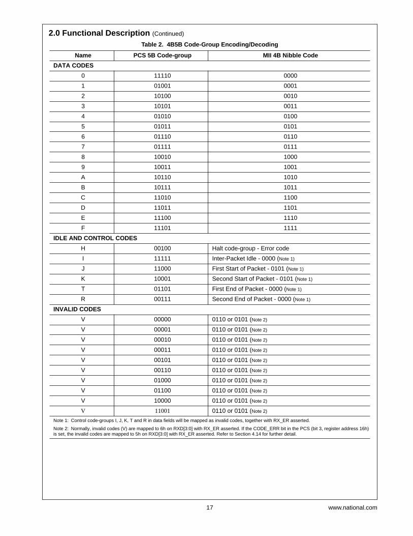
Table 2. 4B5B Code-Group Encoding/Decoding
Name PCS 5B Code-group MII 4B Nibble Code
DATA CODES
0 11110 0000
1 01001 0001
2 10100 0010
3 10101 0011
4 01010 0100
5 01011 0101
6 01110 0110
7 01111 0111
8 10010 1000
9 10011 1001
A 10110 1010
B 10111 1011
C 11010 1100
D 11011 1101
E 11100 1110
F 11101 1111
IDLE AND CONTROL CODES
H 00100 Halt code-group - Error code
I 11111 Inter-Packet Idle - 0000 (Note 1)
J 11000 First Start of Packet - 0101 (Note 1)
K 10001 Second Start of Packet - 0101 (Note 1)
T 01101 First End of Packet - 0000 (Note 1)
R 00111 Second End of Packet - 0000 (Note 1)
INVALID CODES
V 00000 0110 or 0101 (Note 2)
V 00001 0110 or 0101 (Note 2)
V 00010 0110 or 0101 (Note 2)
V 00011 0110 or 0101 (Note 2)
V 00101 0110 or 0101 (Note 2)
V 00110 0110 or 0101 (Note 2)
V 01000 0110 or 0101 (Note 2)
V 01100 0110 or 0101 (Note 2)
V 10000 0110 or 0101 (Note 2)
V 11001 0110 or 0101 (Note 2)
Note 1: Control code-groups I, J, K, T and R in data fields will be mapped as invalid codes, together with RX_ER asserted.
Note 2: Normally, invalid codes (V) are mapped to 6h on RXD[3:0] with RX_ER asserted. If the CODE_ERR bit in the PCS (bit 3, register address 16h)is set, the invalid codes are mapped to 5h on RXD[3:0] with RX_ER asserted. Refer to Section 4.14 for further detail.
2.0 Functional Description (Continued)
18 www.national.com
The 100BASE-TX MLT-3 signal sourced by the TPTD+/−common driver output pins is slow rate controlled. Thisshould be considered when selecting AC coupling magnet-ics to ensure TP-PMD compliant transition times (3 ns < Tr< 5ns).The 100BASE-TX transmit TP-PMD function within theDP83843 is capable of sourcing only MLT-3 encoded data.Binary output from the TPTD+/− outputs is not possible in100 Mb/s mode.2.2.4 TX_ER
Assertion of the TX_ER input while the TX_EN input is alsoasserted will cause the DP83843 to substitute HALT code-groups for the 5B data present at TXD[3:0]. However, theSSD (/J/K/) and ESD (/T/R/) will not be substituted withHalt code-groups. As a result, the assertion of TX_ERwhile TX_EN is asserted will result in a frame properlyencapsulated with the /J/K/ and /T/R/ delimiters which con-tains HALT code-groups in place of the data code-groups.2.2.5 TXAR100
The transmit amplitude of the signal presented at theTPTD+/− output pins can be controlled by varying the valueof resistance between TXAR100 and system GND. ThisTXAR100 resistor sets up a reference current that deter-mines the final output current at TPTD+/−.For 100Ω Category-5 UTP cable implementations, theTXAR100 resistor may be omitted as the DP83843 wasdesigned to source a nominal 2V pk-pk differential transmitamplitude with this pin left floating. Setting the transmitamplitude to 2V pk-pk differential (MLT-3) as measuredacross the RJ45-8 transmit pins is critical for complyingwith the IEEE/ANSI TP-PMD specification of 2.0V pk-pkdifferential ± 5%.2.3 100BASE-TX RECEIVERThe 100BASE-TX receiver consists of several functionalblocks which convert the scrambled MLT-3 125 Mb/s serialdata stream to synchronous 4-bit nibble data that is pro-vided to the MII. Because the 100BASE-TX TP-PMD isintegrated, the differential input pins, TPRD+/−, can bedirectly routed to the AC coupling magnetics.See Figure 5 for a block diagram of the 100BASE-TXreceive function. This provides an overview of each func-tional block within the 100BASE-TX receive section.The Receive section consists of the following functionalblocks:— Input and BLW Compensation— Signal Detect— Digital Adaptive Equalization— MLT-3 to Binary Decoder— Clock Recovery Module— NRZI to NRZ Decoder— Serial to Parallel— DESCRAMBLER (bypass option)— Code Group Alignment— 4B/5B Decoder (bypass option)— Link Integrity Monitor— Bad SSD DetectionThe bypass option for the functional blocks within the100BASE-X receiver provides flexibility for applications
such as 100 Mb/s repeaters where data conversion is notalways required.2.3.1 Input and Base Line Wander Compensation
Unlike the DP83223V TWISTER™, the DP83843 requiresno external attenuation circuitry at its receive inputs,TPRD+/−. The DP83843 accepts TP-PMD compliant wave-forms directly, requiring only a 100Ω termination plus asimple 1:1 transformer. The DP83843 also requires exter-nal capacitance to VCC at the VCM_CAP pin (refer to Fig-ure 23). This establishes a solid common mode voltagethat is needed since the TPRD pins are used in both 10Mb/s and 100 Mb/s modes.The DP83843 is completely ANSI TP-PMD compliantbecause it compensates for baseline wander. The BLWcompensation block can successfully recover the TP-PMDdefined “killer” pattern and pass it to the digital adaptiveequalization block.Baseline wander can generally be defined as the change inthe average DC content, over time, of an AC coupled digitaltransmission over a given transmission medium. (i.e. cop-per wire).Baseline wander results from the interaction between thelow frequency components of a bit stream being transmit-ted and the frequency response of the AC coupling compo-nent(s) within the transmission system. If the low frequencycontent of the digital bit stream goes below the low fre-quency pole of the AC coupling transformers then thedroop characteristics of the transformers will dominateresulting in potentially serious baseline wander.It is interesting to note that the probability of a baseline wan-der event serious enough to corrupt data is very low. In fact,it is reasonable to virtually bound the occurrence of a base-line wander event serious enough to cause bit errors to alegal but premeditated, artificially constructed bit sequenceloaded into the original MAC frame. Several studies havebeen conducted to evaluate the probability of various base-line wander events for FDDI transmission over copper. Con-tact the X3.263 ANSI group for further information.2.3.2 Signal Detect
The signal detect function of the DP83843 is incorporatedto meet the specifications mandated by the ANSI FDDI TP-PMD Standard as well as the IEEE 802.3 100BASE-TXStandard for both voltage thresholds and timing parame-ters.Note that the reception of Normal 10BASE-T link pulsesand fast link pulses per IEEE 802.3u Auto-Negotiation bythe 100BASE-X receiver do not cause the DP83843 toassert signal detect.While signal detect is normally generated and processedentirely within the DP83843, it can be observed directly onthe CRS pin (pin 22) while the DP83843 is configured forSymbol mode. Refer to Section 3.4 for further detail regard-ing Symbol mode operation.2.3.3 Digital Adaptive Equalization
When transmitting data at high speeds over copper twistedpair cable, frequency dependent attenuation becomes aconcern. In high speed twisted pair signalling, the fre-quency content of the transmitted signal can vary greatlyduring normal operation based primarily on the random-ness of the scrambled data stream. This variation in signal

2.0 Functional Description (Continued)
19 www.national.com
Figure 1. Receive Block Diagram
4B/5BDECODER
DESCRAMBLER
DIGITALADAPTIVE
EQUALIZATION
MLT-3 TOBINARY
DECODER
TPRD +/−
RX_CLK RXD[3:0] / RX_ER
INPUT&BLW
COMPEN-SATION
BP_4B5B
BP_SCR
BP_RX
SIGNALDETECT
NRZI TO NRZDECODER
CODE GROUPALIGNMENT
SERIAL TOPARALLEL
MUX
MUX
MUX
SD
CLOCKRECOVERY
MODULE
DATA
CLOCK
RX_DATAVALID SSD
DETECT
CARRIERINTEGRITYMONITOR
LINK INTEG-RITY MONITOR

2.0 Functional Description (Continued)
20 www.national.com
attenuation caused by frequency variations must be com-pensated for to ensure the integrity of the transmission.In order to ensure quality transmission when employingMLT-3 encoding, the compensation must be able to adaptto various cable lengths and cable types depending on theinstalled environment. The selection of long cable lengthsfor a given implementation, requires significant compensa-tion which will over-compensate for shorter, less attenuat-ing lengths. Conversely, the selection of short orintermediate cable lengths requiring less compensation willcause serious under-compensation for longer lengthcables. Therefore, the compensation or equalization mustbe adaptive to ensure proper conditioning of the receivedsignal independent of the cable length.The DP83843 utilizes an extremely robust equalizationscheme referred to herein as ‘Digital Adaptive Equaliza-tion.’ Existing designs use an adaptive equalization schemethat determines the approximate cable length by monitor-ing signal attenuation at certain frequencies. This attenua-tion value was compared to the internal receive inputreference voltage. This comparison would indicate thatamount of equalization to use. Although this scheme isused successfully on the DP83223V TWISTER, it is sensi-tive to transformer mismatch, resistor variation and processinduced offset. The DP83223V also required an externalattenuation network to help match the incoming signalamplitude to the internal reference.Digital Adaptive Equalization is based on an advanced dig-itally controlled signal tracking technique. This methoduses peak tracking with digital over-sampling and digitallycontrolled feedback loops to regenerate the receive signal.This technique does not depend on input amplitude varia-tions to set the equalization factor. As a result it maintainsconstant jitter performance for any cable length up to 150meters of CAT-5. Digital Adaptive Equalization allows forvery high tolerance to signal amplitude variations.The curves given in Figure 6 illustrate attenuation at certainfrequencies for given cable lengths. This is derived from theworst case frequency vs. attenuation figures as specified inthe EIA/TIA Bulletin TSB-36. These curves indicate the sig-nificant variations in signal attenuation that must be com-pensated for by the receive adaptive equalization circuit.Figure 7 represents a scrambled IDLE transmitted overzero meters of cable as measured at the AII (Active InputInterface) of the receiver. Figure 8 and Figure 9 representthe signal degradation over 50 and 100 Meters of CAT-5cable respectively, also measured at the AII. These plotsshow the extreme degradation of signal integrity and indi-cate the requirement for a robust adaptive equalizer.The DP83843 provides the added flexibility of controllingthe type of receive equalization required for a given imple-mentation. This is done through TW_EQSEL (bits [13:12]of the PHYCTRL register, address 19h). While digital adap-tive equalization is the preferred method of cable compen-sation for 100BASE-TX, the ability to switch the equalizercompletely off or to a fixed maximum is provided. This fea-ture is intended as a test mode only and, if enabled, willinhibit normal performance of the DP83843.2.3.4 MLT-3 to NRZI Decoder
The DP83843 decodes the MLT-3 information from the Dig-ital Adaptive Equalizer block to binary NRZI data. The rela-tionship of binary to MLT-3 data is shown in Figure 4.
2.3.5 Clock Recovery Module
The Clock Recovery Module (CRM) accepts 125 Mb/sNRZI data from the MLT-3 to NRZI decoder. The CRM locksonto the 125 Mb/s data stream and extracts a 125 MHz ref-erence clock. The extracted and synchronized clock anddata are used as required by the synchronous receiveoperations as generally depicted in Figure 5.The CRM is implemented using an advanced digital PhaseLocked Loop (PLL) architecture that replaces sensitiveanalog circuits. Using digital PLL circuitry allows theDP83843 to be manufactured and specified to tighter toler-ances.For further information relating to the 100BASE-X clockrecovery module, refer to Section 4.3.
Figure 1. EIA/TIA Attenuation vs Frequency for 0, 50,100 meters of CAT-5 cable
Figure 2. MLT-3 Signal Measured at AII after 0 meters ofCAT-5 cable
100M
50M
0M
tenuation (dB)
4.00
6.00
8.00
10.00
12.00
14.00
16.00
18.00
20.00
22.00
2ns/div

2.0 Functional Description (Continued)
21 www.national.com
2.3.6 NRZI to NRZ
In a typical application, the NRZI to NRZ decoder isrequired in order to present NRZ formatted data to thedescrambler (or to the code-group alignment block, if thedescrambler is bypassed, or directly to the PCS, if thereceiver is bypassed).The receive data stream is in NRZI format, therefore, the datamust be decoded to NRZ before further processing.
2.3.7 Serial to Parallel
The 100BASE-X receiver includes a Serial to Parallel con-verter which supplies 5 bit wide data symbols to theDescrambler. Converting to parallel helps to decreaselatency through the device, as well as performing the
required function for ultimately providing data to the nibble-wide interface of the MII.2.3.8 Descrambler
A 5-bit parallel (code-group wide) descrambler is used todescramble the receive NRZ data. To reverse the datascrambling process, the descrambler has to generate anidentical data scrambling sequence (N) in order to recoverthe original unscrambled data (UD) from the scrambleddata (SD) as represented in the equations:
Synchronization of the descrambler to the original scram-bling sequence (N) is achieved based on the knowledgethat the incoming scrambled data stream consists ofscrambled IDLE data. After the descrambler has recog-nized 12 consecutive IDLE code-groups, where an IDLEcode-group in 5B NRZ is equal to five consecutive ones(11111), it will synchronize to the receive data stream andgenerate unscrambled data in the form of unaligned 5Bcode-groups.In order to maintain synchronization, the descrambler mustcontinuously monitor the validity of the unscrambled datathat it generates. To ensure this, a line state monitor and ahold timer are used to constantly monitor the synchroniza-tion status. Upon synchronization of the descrambler thehold timer starts a 722 µs countdown. Upon detection ofsufficient IDLE code-groups within the 722 µs period, thehold timer will reset and begin a new countdown. This mon-itoring operation will continue indefinitely given a properlyoperating network connection with good signal integrity. Ifthe line state monitor does not recognize sufficientunscrambled IDLE code-groups within the 722 µs period,the entire descrambler will be forced out of the current stateof synchronization and reset in order to re-acquire synchro-nization.The value of the time-out for this timer may be modifiedfrom 722 sto 2 ms by setting bit 12 of the PCSR (address16h) to one. The 2 ms option allows applications with Maxi-mum Transmission Units (packet sizes) larger than IEEE802.3 specifications to maintain descrambler synchroniza-tion (i.e. switch or router applications).Additionally, this timer may be disabled entirely by settingbit 11 of the PCSR (address 16h) to one. The disabling ofthe time-out timer is not recommended as this will eventu-ally result in a lack of synchronization between the transmitscrambler and the receive descrambler which will corruptdata. The descrambler time-out counter may be reset by bit13 of the PCSR.2.3.9 Code-group Alignment
The code-group alignment module operates on unaligned5-bit data from the descrambler (or, if the descrambler isbypassed, directly from the NRZI/NRZ decoder) and con-verts it into 5B code-group data (5 bits). Code-group align-ment occurs after the J/K code-group pair is detected.Once the J/K code-group pair (11000 10001) is detected,subsequent data is aligned on a fixed boundary.2.3.10 4B/5B Decoder
The code-group decoder functions as a look up table thattranslates incoming 5B code-groups into 4B nibbles. Thecode-group decoder first detects the J/K code-group pairpreceded by IDLE code-groups and replaces the J/K with
Figure 1. MLT-3 Signal Measured at AII after 50 metersof CAT-5 cable
Figure 2. MLT-3 Signal Measured at AII after 100 metersof CAT-5 cable
2ns/div
2ns/div
UD SD N⊕( )=SD UD N⊕( )=

2.0 Functional Description (Continued)
22 www.national.com
the MAC preamble. Specifically, the J/K 10-bit code-grouppair is replaced by the nibble pair (0101 0101). All subse-quent 5B code-groups are converted to the corresponding4B nibbles for the duration of the entire packet. This con-version ceases upon the detection of the T/R code-grouppair denoting the End of Stream Delimiter (ESD) or with thereception of a minimum of two IDLE code-groups.2.3.11 100BASE-X Link Integrity Monitor
The 100BASE-X Link Integrity Monitor function (LIM)allows the receiver to ensure that reliable data is beingreceived. Without reliable data reception, the LIM will haltboth transmit and receive operations until such time that avalid link is detected (i.e. good link).If Auto-Negotiation is not enabled, then a valid link will beindicated once SD+/− is asserted continuously for 500 µs.If Auto-Negotiation is enabled, then Auto-Negotiation willfurther qualify a valid link as follows:— The descrambler must receive a minimum of 12 IDLE
code groups for proper link initialization.— The Auto-Negotiation must determine that the
100BASE-X function should be enabled.A valid link for a non-Auto-Negotiating application is indi-cated by either the Link LED output or by reading bit 2 ofthe Basic Mode Status Register BMSR (address 01h). Fora truly qualified valid link indication as a result of Auto-Negotiation, bit 2 of the BMSR register (address 01h) mustbe read.2.3.12 Bad SSD Detection
A Bad Start of Stream Delimiter (Bad SSD) is any transitionfrom consecutive idle code-groups to non-idle code-groupswhich is not prefixed by the code-group pair /J/K.If this condition is detected, the DP83843 will assertRX_ER and present RXD[3:0] = 1110 to the MII for thecycles that correspond to received 5B code-groups. Inorder to exit this state the PHYTER must receive at leasttwo IDLE code groups and the PHYTER cannot receive asingle IDLE code group at any time. In addition, the FalseCarrier Event Counter (address 14h) will be incrementedby one. Once the PHYTER exits this state, RX_ER andCRS become de-asserted.When bit 11 of the LBR register is one (BP_RX), RXD[3:0]and RX_ER/RXD[4] are not modified.2.3.13 Carrier Integrity Monitor
The Carrier Integrity Monitor function (CIM) protects therepeater from transient conditions that would otherwisecause spurious transmission due to a faulty link. This func-tion is required for repeater applications and is not speci-fied for node applications.The REPEATER pin (pin 63) determines the default state ofbit 5 of the PCS register (Carrier Integrity Monitor Disable,address 16h) to automatically enable or disable the CIMfunction as required for IEEE 802.3 compliant applications.After power-up/reset, software may enable or disable thisfunction independent of Repeater or Node mode.If the CIM determines that the link is unstable, theDP83843 will not propagate the received data or controlsignaling to the MII and will ignore data transmitted via theMII. The DP83843 will continue to monitor the receivestream for valid carrier events.
Detection of an unstable link condition will cause bit 4 ofthe PCS register (address 16h) to be set to one. This bit iscleared to zero upon a read operation once a stable linkcondition is detected by the CIM. Upon detection of a sta-ble link, the DP83843 will resume normal operations.The Disconnect Counter (address 13h) increments eachtime the CIM determines that the link is unstable.2.4 10BASE-T TRANSCEIVER MODULEThe 10BASE-T Transceiver Module is IEEE 802.3 compli-ant. It includes the receiver, transmitter, collision, heart-beat, loopback, jabber, and link integrity functions, asdefined in the standard. An external filter is not required onthe 10BASE-T interface since this is integrated inside theDP83843. Due to the complexity and scope of the10BASE-T Transceiver block and various sub-blocks, thissection focuses on the general system level operation.2.4.1 Operational Modes
The DP83843 has 2 basic 10BASE-T operational modes:Half Duplex modeFull Duplex mode
Half Duplex Mode
In Half Duplex mode the DP83843 functions as a standardIEEE 802.3 10BASE-T transceiver supporting theCSMA/CD protocol.Full Duplex Mode
In Full Duplex mode the DP83843 is capable of simulta-neously transmitting and receiving without asserting thecollision signal. The DP83843's 10 Mb/s ENDEC isdesigned to encode and decode simultaneously.2.4.2 Oscillator Module Operation
A 25 MHz crystal or can-oscillator with the following specifi-cations is recommended for driving the X1 input.1. CMOS output with a 50ppm frequency tolerance.2. 35-65% duty cycle (max).3. Two TTL load output drive.Additional output drive may be necessary if the oscillatormust also drive other components. When using a clockoscillator it is still recommended that the designer connectthe oscillator output to the X1 pin and leave X2 floating.2.4.3 Smart Squelch
The smart squelch is responsible for determining whenvalid data is present on the differential receive inputs(TPRD+/−). The DP83843 implements an intelligentreceive squelch to ensure that impulse noise on the receiveinputs will not be mistaken for a valid signal. Smart squelchoperation is independent of the 10BASE-T operationalmode.The squelch circuitry employs a combination of amplitudeand timing measurements (as specified in the IEEE 802.310BASE-T standard) to determine the validity of data onthe twisted pair inputs (refer to Figure 10).The signal at the start of packet is checked by the smartsquelch and any pulses not exceeding the squelch level(either positive or negative, depending upon polarity) willbe rejected. Once this first squelch level is overcome cor-rectly, the opposite squelch level must then be exceededwithin 150 ns. Finally the signal must exceed the originalsquelch level within a further 150 ns to ensure that the

2.0 Functional Description (Continued)
23 www.national.com
input waveform will not be rejected. The checking proce-dure results in the loss of typically three preamble bits atthe beginning of each packet.Only after all these conditions have been satisfied will acontrol signal be generated to indicate to the remainder ofthe circuitry that valid data is present. At this time, thesmart squelch circuitry is reset.Valid data is considered to be present until squelch levelhas not been generated for a time longer than 150ns, indi-cating the End of Packet. Once good data has beendetected the squelch levels are reduced to minimize theeffect of noise causing premature End of Packet detection.The receive squelch threshold level can be lowered for usein longer cable applications. This is achieved by setting theLS_SEL bit in the 10BTSCR (bit 6, register 18h). CollisionDetectionFor Half Duplex, a 10BASE-T collision is detected when thereceive and transmit channels are active simultaneously.Collisions are reported by the COL signal on the MII.If the ENDEC is transmitting when a collision is detected,the collision is not reported until seven bits have beenreceived while in the collision state. This prevents a colli-sion being reported incorrectly due to noise on the network.The COL signal remains set for the duration of the collision.If the ENDEC is receiving when a collision is detected it isreported immediately (through the COL).When heartbeat is enabled, approximately 1 µs after thetransmission of each packet, a Signal Quality Error (SQE)signal of approximately 10 bit times is generated (inter-nally) to indicate successful transmission. SQE is reportedas a pulse on the COL signal of the MII.2.4.4 Carrier Sense
Carrier Sense (CRS) may be asserted due to receive activ-ity once valid data is detected via the smart squelch func-tion.For 10 Mb/s Half Duplex operation, CRS is asserted duringeither packet transmission or reception.For 10 Mb/s Full Duplex operation, CRS is asserted onlydue to receive activity.CRS is deasserted following an end of packet.In Repeater mode, CRS is only asserted due to receiveactivity.
2.4.5 Normal Link Pulse Detection/Generation
The link pulse generator produces pulses as defined in theIEEE 802.3 10BASE-T standard. Each link pulse is nomi-nally 100 ns in duration and is transmitted every 16 ms ± 8ms, in the absence of transmit data.Link pulse is used to check the integrity of the connectionwith the remote end. If valid link pulses are not received,the link detector disables the 10BASE-T twisted pair trans-mitter, receiver and collision detection functions.When the link integrity function is disabled, the 10BASE-Ttransceiver will operate regardless of the presence of linkpulses.2.4.6 Jabber Function
The jabber function monitors the DP83843's output anddisables the transmitter if it attempts to transmit a packet oflonger than legal size. A jabber timer monitors the transmit-ter and disables the transmission if the transmitter is activefor approximately 20-30 ms.Once disabled by the Jabber function, the transmitter staysdisabled for the entire time that the ENDEC module's inter-nal transmit enable is asserted. This signal has to be de-asserted for approximately 400-600 ms (the “unjab” time)before the Jabber function re-enables the transmit outputs.The Jabber function is only meaningful in 10BASE-T mode.2.4.7 Status Information
10BASE-T Status Information is available on the LED out-put pins of the DP83843. Transmit activity, receive activity,link status, link polarity and collision activity information isoutput to the five LED output pins (LED_RX, LED_TX,LED_LINK, LED_FDPOL, and LED_COL). Additionally, theactive high SPEED10 output will assert to indicate 10 Mb/soperation.If required, the LED outputs can be used to provide digitalstatus information to external circuitry.The link LED output indicates good link status for both 10and 100 Mb/s modes. In Half Duplex 10BASE-T mode,LED_LINK indicates link status.The link integrity function can be disabled. When disabled,the transceiver will operate regardless of the presence oflink pulses and the link LED will stay asserted continuously.2.4.8 Automatic Link Polarity Detection
The DP83843's 10BASE-T transceiver module incorpo-rates an automatic link polarity detection circuit. Whenseven consecutive link pulses or three consecutive receive
Figure 1. 10BASE-T Twisted Pair Smart Squelch Operation
<150ns <150ns >150ns
start of packet end of packet
Vsq +
Vsq -
Vsq +reduced
Vsq -reduced
Twisted Pair Squelch Operation

2.0 Functional Description (Continued)
24 www.national.com
packets with inverted End-of-Packet pulses are received,bad polarity is reported.A polarity reversal can be caused by a wiring error at eitherend of the cable, usually at the Main Distribution Frame(MDF) or patch panel in the wiring closet.The bad polarity condition is latched and the LED_ FDPOLoutput is asserted. The DP83843's 10BASE-T transceivermodule corrects for this error internally and will continue todecode received data correctly. This eliminates the need tocorrect the wiring error immediately.2.4.9 10BASE-T Internal Loopback
When the 10MB_ENDEC_LB bit in the LBR (bit 4, registeraddress 17h) is set, 10BASE-T transmit data is loopedback in the ENDEC to the receive channel. The transmitdrivers and receive input circuitry are disabled in trans-ceiver loopback mode, isolating the transceiver from thenetwork.Loopback is used for diagnostic testing of the data paththrough the transceiver without transmitting on the networkor being interrupted by receive traffic. This loopback func-tion causes the data to loopback just prior to the 10BASE-Toutput driver buffers such that the entire transceiver path istested.2.4.10 Transmit and Receive Filtering
External 10BASE-T filters are not required when using theDP83843 as the required signal conditioning is integrated.Only isolation/step-up transformers and impedance match-ing resistors are required for the 10BASE-T transmit andreceive interface. The internal transmit filtering ensuresthat all the harmonics in the transmit signal are attenuatedby at least 30 dB.2.4.11 Encoder/Decoder (ENDEC) Module
The ENDEC module consists of essentially four functions:The oscillator generates the 10 MHz transmit clock signalfor system timing from an external 25 MHz oscillator.The Manchester encoder accepts NRZ data from the con-troller or repeater, encodes the data to Manchester, andtransmits it differentially to the transceiver, through the dif-ferential transmit driver.The Manchester decoder receives Manchester data fromthe transceiver, converts it to NRZ data and recovers clockpulses for synchronous data transfer to the controller orrepeater.The collision monitor indicates to the controller the pres-ence of a valid 10 Mb/s collision signal.
2.4.12 Manchester Encoder
The encoder begins operation when the Transmit Enableinput (TX_EN) goes high and converts the NRZ data topre-emphasized Manchester data for the transceiver. Forthe duration of TX_EN remaining high, the Transmit Data(TPTD+/−) is encoded for the transmit-driver pair(TPTD+/−). TXD must be valid on the rising edge of Trans-mit Clock (TX_CLK). Transmission ends when TX_ENdeasserts. The last transition is always positive; it occurs atthe center of the bit cell if the last bit is a one, or at the endof the bit cell if the last bit is a zero.2.4.13 Manchester Decoder
The decoder consists of a differential receiver and a PLL toseparate a Manchester encoded data stream into internalclock signals and data. The differential input must be exter-nally terminated with either a differential 100ohm termina-tion network to accommodate UTP cable.The decoder detects the end of a frame when no more mid-bit transitions are detected. Within one and a half bit timesafter the last bit, carrier sense is de-asserted. Receiveclock stays active for five more bit times after CRS goeslow, to guarantee the receive timings of the controller orrepeater.2.5 100 BASE-FXThe DP83843 is fully capable of supporting 100BASE-FXapplications. 100BASE-FX is similar to 100BASE-TX withthe exceptions being the PMD sublayer, lack of data scram-bling, and signaling medium and connectors. Chapter 26 ofthe IEEE 802.3u specification defines the interface to thisPMD sublayer.The DP83843 can be configured for 100BASE-FX opera-tion either through hardware or software. Configurationthrough hardware is accomplished by forcing the FXEN pin(pin 21) to a logic low level prior to power-up/reset. Config-uration through software is accomplished by setting bits 9:7of the LBR register to <011>, enabling FEFI (bit 14 of regis-ter PCSR(16h)), bypassing the scrambler (bit 12 of registerLBR(17h)) and disabling Auto-Negotiation. In addition, set-ting the FX_EN bit of the PHYCTRL register (bit 5, address19h) accomplishes the same function as forcing the FXENpin (pin 21) to a logic low. In 100BASE-FX mode, the FXinterface is enabled along with the Far End Fault Indication(FEFI) and Bypass Scrambler functions. Auto-Negotiationmust be disabled in order for 100BASE-FX operation towork properly .The diagram in Figure 11 is a block diagram representationof the FX interface and the alternative data paths for trans-mit, receive and signal detect.
2.0 Functional Description (Continued)
25 www.national.com
2.5.1 FX Interface
When the FX interface is enabled the internal 100BASE-TXtransceiver is disabled. As defined by the 802.3u specifica-tion, PMD_SIGNAL_indicate (signal detect function),PMD_UNITDATA.indicate (receive function), andPMD_UNIT_DATA.request (transmit function) are sup-ported by the FXSD+/−, FXRD+/−, and FXTD+/− pinsrespectively.Transmit
The DP83843 transmits NRZI data on the FXTD+/− pins.This data is transmitted at PECL signal levels. 100BASE-FX requires no scrambling/de-scrambling, so the scrambleris bypassed in the transmit path. All other PMA and PCSfunctions remain unaffected.Receive
The DP83843 receives NRZI data on the FXRD+/− pins.This data is accepted at PECL signal levels. 100BASE-FXrequires no scrambling/de-scrambling, so the de-scrambleris bypassed in the receive path. All other PMA and PCSfunctions remain unaffected.Signal Detect
The DP83843 receives signal detect information on theFXSD+/− pins. This data is accepted at PECL signal levels.Signal detect indicates that a signal with the proper ampli-tude is present at the PMD sublayer.2.5.2 Far End Fault Indication
Auto-Negotiation provides a mechanism for transferringinformation from the Local Station to the Link Partner that aremote fault has occurred for 100BASE-TX. As Auto-Nego-
tiation is not currently specified for operation over fiber, theFar End Fault Indication function (FEFI) provides somedegree of communication between link partners in supportof 100BASE-FX operation.A remote fault is an error in the link that one station candetect while the other cannot. An example of this is a dis-connected fiber at a station’s transmitter. This station willbe receiving valid data and detect that the link is good viathe Link Integrity Monitor, but will not be able to detect thatits transmission is not propagating to the other station.A 100BASE-FX station that detects such a remote fault(through the deassertion of signal detect) may modify itstransmitted IDLE stream from all ones to a group of 84ones followed by a single zero (i.e. 16 IDLE code groupsfollowed by a single Data 0 code group). This is referred toas the FEFI IDLE pattern. Transmission of the FEFI IDLEpattern will continue until FXSD+/− is re-asserted.If three or more FEFI IDLE patterns are detected by theDP83843, then bit 4 of the Basic Mode Status register(address 01h) is set to one until read by management. It isalso set in bit 7 of the PHY Status register (address 10h).The first FEFI IDLE pattern may contain more than 84 onesas the pattern may have started during a normal IDLEtransmission which is actually quite likely. However, sinceFEFI is a repeating pattern, this will not cause a problemwith the FEFI function. It should be noted receipt of theFEFI IDLE pattern will not cause CRS to assert.To enable Fiber mode without FEFI, set bits 9:7 of the LBRregister to <011>, disable FEFI (bit 14 of registerPCSR(16h)), bypass the scrambler (bit 12 of register
Figure 1. 100Base-FX Block Diagram
NRZ TO NRZIENCODER
BINARYTO MLT-3 /COMMONDRIVER
PECLDRIVER
FXTD
TPRD+/−
INPUT &BLW COMP
FULL ADAPT. EQUALIZ.
MLT-3 TO BINARY DEC.
SIGNALDETECT
CLOCKRECOVERY
MODULE
PECLINPUTS
FXSDFXRD
NORMAL TX DATAW/ SCRAMBLER BYPASSED
NORMAL RX DATA TO DESCRAMBLER BYPASS
NORMALSIGNAL DETECT
TPTD+/−

2.0 Functional Description (Continued)
26 www.national.com
LBR(17h)) and disable Auto-Negotiation. Without FEFIenabled the DP83843 will not send the FEFI idle pattern.Additionally, upon detection of Far End Fault, all receiveand transmit MII activity is disabled/ignored (MII serialmanagement is unaffected).
This function is optional for 100BASE-FX compliance andshould be disabled for 100BASE-TX compliance. If Auto-Negotiation is enabled (bit 12 of the BMCR) then FEFI isautomatically disabled. FEFI is automatically enabled whenthe DP83843 is configured for 100BASE-FX operation.
2.5.3 Software Enable
The FX functions can also be set via software. The FX-interface is set by bit 5 of the PHYCTRL register (address19h). The FEFI_EN function is set by bit 14 of register 16h.The bypass scrambler and de-scrambler function is set bybit 11 of the loopback and bypass register (address 17h).2.5.4 FX Interface Considerations
The termination and signal routing for the high-speedPECL signals are critical. The following diagram shows atypical thevenin termination circuit.Chapter 26 of the 802.3u 100BASE-X document includesreferences to the three most common types of 125 Mb/soptical transceiver connectors available. The DP83843 maybe used with any of these three connectors.It is important to note that the typical 9-pin low cost fibertransceiver utilizes a single-ended PECL output for SignalDetect indication. Since the DP83843 incorporates stan-dard differential PECL inputs for Signal Detect, the FXSD-input (pin 47) can be externally biased as depicted inFigure 12 to ensure proper operation.Optionally, the proper bias potential for FXSD- can be gen-erated by the DP83843 internally. This is accomplished bysetting bit 15 of register 16 (PCSR). This option eliminatesthe requirement for additional external passive componentswhich would otherwise be required for the proper biasing ofFXSD- in an application where only a single-ended SD sig-nal is available.2.6 AUIThe DP83843 is capable of operating in 10BASE-2 and10BASE-5 applications. This is done by utilizing the AUI(Attachment Unit Interface) pins of the DP83843. The AUIinterface is completely IEEE 802.3 compliant. SeeFigure 14 for an example of a typical AUI connector setup.
AUI mode is selected by bit 5 (AUI_SEL) of the 10BASE-TControl and Status register (10BTSCR). It can also be acti-vated by the Autoswitch feature explained below.Autoswitch overrides the AUI_SEL bit. The Status of theport, either AUI or TP mode, is displayed in bit 12(AUI_TPI) of the 10BTSCR register.2.6.1 AUI Block Diagram
The pins at the AUI interface are AUIRD+/−, AUITD+/−, andAUICD+/−. They provide the Read, Transmit and CollisionDetect functions respectively. See Figure 13 for a block dia-gram of the AUI interface. The AUI interface includes the
PLL Decoder, Collision Decoder and Manchester Encoderand Driver.The PLL Decoder receives Manchester data from thetransceiver, converts it to NRZ data and clock pulses andsends it to the controller.The collision decoder indicates to the MII the presence of avalid 10 MHz collision signal to the PLL.
Figure 1. Typical DP83843 to Optical Transceiver Interfaces
9-pin Optical Transceiver
DP83843 100BASE-FX
FXRD+/-
FXTD+/-
FXSD+/-
RX_DATA+/-
Signal_Detect +
TX_DATA+/-
VCC
130Ω
PECL Thevenin Termination
RX
TX
50
43
48
49
47
44130Ω
130Ω 130Ω
115Ω
115Ω
370Ω
82Ω
82Ω 82Ω 90Ω
90Ω
Figure 1. AUI Block Diagram
PLL
AUIRD+/- AUICD+/- AUITD+/-
DecoderCollisionDecoder
ManchesterEncoder& Driver
MII Interface/Control
rx_clkrx_data
crs col_detect
tx_data tx_clk

2.0 Functional Description (Continued)
27 www.national.com
The Manchester encoder accepts NRZ data from the MII,encodes the data to Manchester and sends it to the driver.The driver transmits the data differentially to the trans-ceiver.2.6.2 AUI/TP Autoswitch
The DP83843 has an autoswitching feature that allowsswitching between the AUI and TP operation. The AUI/TPIautoswitch feature (AUTOSW_EN) is enabled by bit 9 ofthe 10BASE-T Control and Status Register (10BTSCR). IfAUTOSW_EN is asserted (default is de-asserted) and theDP83843 is in 10 Mb/s mode it automatically activates theTPI interface (10 Mb/s data is transmitted and received atthe TPTD+/− and TPRD+/− pins respectively). If there is anabsence of link pulses, the transceiver will switch to AUImode. Similarly, when the transceiver starts detecting linkpulses it will switch to TP mode. The switching from onemode to the next is only done after the current packet hasbeen transmitted or received. If the twisted pair output isjabbering and gets into link fail state, then the switch to AUImode is only done after the jabbering is done, including thetime it takes to unjab (unjab time).2.6.3 Ethernet Cable Configuration / THIN Output
The DP83843 offers the choice of Thick Ethernet(10BASE5) and Thin Ethernet (10BASE-2). The type ofcabling used is controlled through bit 3 of the 10BTSCRregister (address 18h). The DP83843 also provides a THINoutput signal which can be used to disable/enable an exter-nal DC-DC converter which is required for 10BASE-2 appli-cations to provide electrical isolation. This enables a10BASE-2 and10BASE-5 common interface application.
Figure 1. AUI Typical Setup
15 Pin D AUI Connector
100uH
39Ω
39Ω39Ω
39Ω
.01uf
.01uf
AUITD AUIRD AUICD
200Ω 200Ω

28 www.national.com
3.0 Configuration
This section includes information on the various configura-tion options available with the DP83843. The configurationoptions described herein include:— Auto-Negotiation— PHY Address and LEDs— Half Duplex vs Full Duplex— 100M Symbol mode— 100BASE-FX mode— 10M serial MII mode— 10M AUI Mode— Repeater vs. Node— Isolate mode— Loopback mode3.1 Auto-NegotiationThe Auto-Negotiation function provides a mechanism forexchanging configuration information between two ends ofa link segment and automatically selecting the highest per-formance mode of operation supported by both devices.Fast Link Pulse (FLP) Bursts provide the signaling used tocommunicate Auto-Negotiation abilities between twodevices at each end of a link segment. For further detailregarding Auto-Negotiation, refer to clause 28 of the IEEE802.3u specification. The DP83843 supports four differentEthernet protocols (10 Mb/s Half Duplex, 10 Mb/s FullDuplex, 100 Mb/s Half Duplex, and 100 Mb/s Full Duplex),so the inclusion of Auto-Negotiation ensures that the high-est performance protocol will be selected based on theability of the Link Partner. The Auto-Negotiation functionwithin the DP83843 can be controlled either by internalregister access or by use of the AN1 and AN0 (pins 3 & 4).3.1.1 Auto-Negotiation Pin Control
The state of AN0 and AN1 determines whether theDP83843 is forced into a specific mode or Auto-Negotiationwill advertise a specific ability (or set of abilities) as given inTable 3. Pins AN0 and AN1 are implemented as three-levelcontrol pins which are configured by connecting them toVCC, GND, or by leaving them unconnected (refer to
Figure 15). These pins allow configuration options to beselected without requiring internal register access.It should be noted that due to the internal resistor networksdepicted in Figure 15, the AN0 or AN1 should be con-nected directly to either VCC or GND, depending on therequirements. These pins should never be resistively tied toVCC or GND as this will interfere with the internal pull-upand pull-down resistors resulting in improper Auto-Negotia-tion behavior.The state of AN0 and AN1, upon power-up/reset, deter-mines the state of bit 9 in the PHYSTS register (address10h) as well as bits [8:5] of the ANAR register (address04h).Upon power-up/reset the DP83843 uses default registervalues, which enables Auto-Negotiation and advertises thefull set of abilities (10 Mb/s Half Duplex, 10 Mb/s FullDuplex, 100 Mb/s Half Duplex, and 100 Mb/s Full Duplex)unless subsequent software accesses modify the mode.The status of Auto-Negotiation as a function of hardwareconfiguration via the AN0 and AN1 pins is reflected in bit 9of the PHYSTS register (address 10h).The Auto-Negotiation function selected at power-up orreset can be changed at any time by writing to the BasicMode Control Register (BMCR) at address 00h.3.1.2 Auto-Negotiation Register Control
When Auto-Negotiation is enabled, the DP83843 transmitsthe abilities programmed into the Auto-Negotiation Adver-tisement register (ANAR) at address 04h via FLP Bursts.Any combination of 10 Mb/s, 100 Mb/s, Half-Duplex, andFull Duplex modes may be selected. The default setting ofbits [8:5] in the ANAR and bit 9 in the PHYSTS register(address 10h) are determined at power-up or hard reset bythe state of the AN0 and AN1 pins.The BMCR provides software with a mechanism to controlthe operation of the DP83843. However, the AN0 and AN1pins do not affect the contents of the BMCR and cannot beused by software to obtain status of the mode selected.Bits1 & 2 of the PHYSTS register (address 10h) are only validif Auto-Negotiation is disabled or after Auto-Negotiation iscomplete.
The contents of the ANLPAR register are used to automati-cally configure to the highest performance protocolbetween the local and far-end ports. Software can deter-mine which mode has been configured by Auto-Negotiation
by comparing the contents of the ANAR and ANLPAR reg-isters and then selecting the technology whose bit is set inboth the ANAR and ANLPAR of highest priority relative tothe following list.
Figure 15. 3 Level Hardware Configuration Pin Control
DE
CO
DE
R
-
+
-
+R
R
GND
VL
OUT
A
B
VIN
VCCVH
VIN A B OUT
0V L L L
VCC /2 L H M
VCC H H H

3.0 Configuration (Continued)
29 www.national.com
Auto-Negotiation Priority Resolution:— (1) 100BASE-TX Full Duplex (Highest Priority)— (2) 100BASE-TX Half Duplex— (3) 10BASE-T Full Duplex— (4) 10BASE-T Half Duplex (Lowest Priority)The Basic Mode Control Register (BMCR) at address 00hprovides control of enabling, disabling, and restarting of theAuto-Negotiation function. When Auto-Negotiation is dis-abled the Speed Selection bit in the BMCR (bit 13, registeraddress 00h) controls switching between 10 Mb/s or 100Mb/s operation, while the Duplex Mode bit (bit 8, registeraddress 00h) controls switching between full duplex opera-tion and half duplex operation. The Speed Selection andDuplex Mode bits have no effect on the mode of operationwhen the Auto-Negotiation Enable bit (bit 12, registeraddress 00h) is set.The Basic Mode Status Register (BMSR) at address 01hindicates the set of available abilities for technology types(bits 15 to 11, register address 01h), Auto-Negotiation abil-ity (bit 3, register address 01h), and Extended RegisterCapability (bit 0, register address 01h). These bits are per-manently set to indicate the full functionality of theDP83843 (only the 100BASE-T4 bit is not set since theDP83843 does not support that function, while it does sup-port all the other functions).The BMSR also provides status on:— Whether Auto-Negotiation is complete (bit 5, register ad-
dress 01h)
— Whether the Link Partner is advertising that a remotefault has occurred (bit 4, register address 01h)
— Whether a valid link has been established (bit 2, registeraddress 01h)
— Support for Management Frame Preamble suppression(bit 6, register address 01h)
The Auto-Negotiation Advertisement Register (ANAR) ataddress 04h indicates the Auto-Negotiation abilities to beadvertised by the DP83843. All available abilities are trans-mitted by default, but any ability can be suppressed by writ-ing to the ANAR. Updating the ANAR to suppress an abilityis one way for a management agent to change (force) thetechnology that is used.The Auto-Negotiation Link Partner Ability Register(ANLPAR)at address 05h is used to receive the base linkcode word as well as all next page code words during thenegotiation. Furthermore, the ANLPAR will be updated toeither 0081h or 0021h for parallel detection to either 100Mb/s or 10 Mb/s respectively.If Next Page is NOT being used, then the ANLPAR willstore the base link code word (link partner's abilities) andretain this information from the time the page is received,as indicated by a 1 in bit 1 of the Auto-Negotiation Expan-sion Register (ANER, register address 06h), through theend of the negotiation and beyond.When using the next page operation, the DP83843 cannotwait for Auto-Negotiation to complete in order to read theANLPAR because the register is used to store both the
Table 3. Auto-Negotiation Mode Select
AN1(Pin 3)
AN0(Pin 4)
Action Mode
FORCED MODES
0 M PHYSTS (10h) Bit 9 = 0, Bit 1 = 1, Bit 2 = 0ANAR (04h) [8:0] = 021h
10BASE-T, Half-Duplex without Auto-Negotiation
1 M PHYSTS (10h) Bit 9 = 0, Bit 1 = 1, Bit 2 = 1ANAR (04h) [8:0] = 041h
10BASE-T, Full Duplex without Auto-Negotiation
M 0 PHYSTS (10h) Bit 9 = 0, Bit 1 = 0, Bit 2 = 0ANAR (04h) [8:0] = 081h
100BASE-X, Half-Duplex without Auto-Negotia-tion
M 1 PHYSTS (10h) Bit 9 = 0, Bit1 = 0, Bit 2 = 1ANAR (04h) [8:0] = 101h
100BASE-X, Full Duplex without Auto-Negotia-tion
ADVERTISED MODES
M M PHYSTS (10h) Bit 9 = 1ANAR (04h) [8:0] = 1E1h
All capable (i.e. Half-Duplex & Full Duplex for10BASE-T and 100BASE-TX) advertised viaAuto-Negotiation
0 0 PHYSTS (10h) Bit 9 = 1ANAR (04h) [8:0] = 061h
10BASE-T, Half-Duplex & Full Duplex advertisedvia Auto-Negotiation
0 1 PHYSTS (10h) Bit 9 = 1ANAR (04h) [8:0] = 181h
100BASE-TX, Half-Duplex & Full Duplex adver-tised via Auto-Negotiation
1 0 PHYSTS (10h) Bit 9 = 1ANAR (04h) [8:0] = 0A1h
10BASE-T & 100BASE-TX, Half-Duplex adver-tised via Auto-Negotiation
1 1 PHYSTS (10h) Bit 9 = 1ANAR (04h) [8:0] = 021h
10 BASE-T, Half-Duplex advertised via Auto-Ne-gotiation.
Note: “M” indicates logic mid level (Vcc/2), “1” indicates logic high level, “0” indicates logic low level.

3.0 Configuration (Continued)
30 www.national.com
base and next pages. Software must be available to per-form several functions. The ANER (register 6) must have apage received (bit 1), once the DP83843 receives the firstpage, software must store it in memory if it wants to keepthe information. Auto-Negotiation keeps a copy of the basepage information but it is no longer accessible by software.After reading the base page information, software needs towrite to ANNPTR (register 7) to load the next page informa-tion to be sent. Continue to poll the page received bit in theANER and when active read the ANLPAR. The contents ofthe ANLPAR will tell if the partner has further pages to besent. As long as the partner has more pages to send, soft-ware must write to the next page transmit register and loadanother page.The Auto-Negotiation Expansion Register (ANER) ataddress 06h indicates additional Auto-Negotiation status.The ANER provides status on:— Whether a Parallel Detect Fault has occurred (bit 4, reg-
ister address 06h)— Whether the Link Partner supports the Next Page func-
tion (bit 3, register address 06h)— Whether the DP83843 supports the Next Page function
(bit 2, register address 06h). The DP83843 does supportthe Next Page function.
— Whether the current page being exchanged by Auto-Ne-gotiation has been received (bit1, register address 06h)
— Whether the Link Partner supports Auto-Negotiation (bit0, register address 06h)
The Auto-Negotiation Next Page Transmit Register(ANNPTR) at address 07h contains the next page codeword to be sent. See Table 13 for a bit description of thisregister.3.1.3 Auto-Negotiation Parallel Detection
The DP83843 supports the Parallel Detection function asdefined in the IEEE 802.3u specification. Parallel Detectionrequires both the 10 Mb/s and 100 Mb/s receivers to moni-tor the receive signal and report link status to the Auto-Negotiation function. Auto-Negotiation uses this informa-tion to configure the correct technology in the event that theLink Partner does not support Auto-Negotiation yet istransmitting link signals that the 100BASE-X or 10BASE-TPMAs recognize as valid link signals.The Auto-Negotiation function will only accept a valid linksignal for the purpose of Parallel Detection from PMAswhich have a corresponding bit set in the Auto-NegotiationAdvertisement register, (ANAR register bits 5 and 7,address 04h.) This allows the DP83843 to be configuredfor 100 Mb/s only, 10 Mb/s only, or 10 Mb/s & 100 Mb/sCSMA/CD operation depending on the advertised abilities.The state of these bits may be modified via the AN0 andAN1 pins or by writing to the ANAR. For example, if bit 5 iszero, and bit 7 is one in the ANAR (i.e. 100 Mb/s CSMA/CDonly), and the Link Partner is 10BASE-T without Auto-Negotiation, then Auto-Negotiation will not complete sincethe advertised abilities and the detected abilities have nocommon mode. This operation allows the DP83843 to beused in single mode (i.e. repeater) applications as well asdual mode applications (i.e. 10/100 nodes or switches).If the DP83843 completes Auto-Negotiation as a result ofParallel Detection, without Next Page operation, bits 5 and7 within the ANLPAR register (register address 05h) will beset to reflect the mode of operation present in the Link Part-
ner. Note that bits 4:0 of the ANLPAR will also be set to00001 based on a successful parallel detection to indicatea valid 802.3 selector field. Software may determine thatnegotiation completed via Parallel Detection by reading azero in the Link Partner Auto-Negotiation Able bit (bit 0,register address 06h) once the Auto-Negotiation Completebit (bit 5, register address 01h) is set. If configured for par-allel detect mode and any condition other than a singlegood link occurs then the parallel detect fault bit will set (bit4, register 06h).3.1.4 Auto-Negotiation Restart
Once Auto-Negotiation has completed, it may be restartedat any time by setting bit 9 of the BMCR to one. If the modeconfigured by a successful Auto-Negotiation loses a validlink, then the Auto-Negotiation process will resume andattempt to determine the configuration for the link. Thisfunction ensures that a valid configuration is maintained ifthe cable becomes disconnected.A renegotiation request from any entity, such as a manage-ment agent, will cause the DP83843 to halt any transmitdata and link pulse activity until the break_link_timerexpires (~1500ms). Consequently, the Link Partner will gointo link fail and normal Auto-Negotiation resumes. TheDP83843 will resume Auto-Negotiation after thebreak_link_timer has expired by issuing FLP (Fast LinkPulse) bursts.3.1.5 Enabling Auto-Negotiation via Software
It is important to note that if the DP83843 has been initial-ized upon power-up as a non-auto-negotiating device(forced technology), and it is then required that Auto-Nego-tiation or re-Auto-Negotiation be initiated via software, bit12 of the Basic Mode Control Register (address 00h) mustfirst be cleared and then set for any Auto-Negotiation func-tion to take effect.3.1.6 Auto-Negotiation Complete Time
Parallel detection and Auto-Negotiation take approximately2-3 seconds to complete. In addition, Auto-Negotiation withnext page should take approximately 2-3 seconds to com-plete, depending on the number of next pages sent.Refer to chapter 28 of the IEEE 802.3u standard for a fulldescription of the individual timers related to Auto-Negotia-tion.Auto-Negotiation Next Page Support
The DP83843 supports the optional Auto-Negotiation NextPage protocol. The ANNPTR register (address 07h) allowsfor the configuration and transmission of Next Page. Referto clause 28 of the IEEE 802.3u standard for detailed infor-mation regarding the Auto-Negotiation Next Page function.3.2 PHY Address and LEDsThe DP83843 maps the 5 PHY address input pins onto the5 LED output pins as:
LED_COL <=> PHYAD[0]LED_TX <=> PHYAD[1]LED_RX <=> PHYAD[2]LED_LINK <=> PHYAD[3]LED_FDPOL <=> PHYAD[4]
The DP83843 can be set to respond to any of 32 possiblePHY addresses. Each DP83843 connected to a commonserial MII must have a unique address. It should be noted
3.0 Configuration (Continued)
31 www.national.com
that while an address selection of all zeros <00000> willresult in PHY Isolate mode, this will not effect serial man-agement access.The state of each of the PHYAD inputs are latched into thePHYCTRL register bits [4:0] (address 19h) at systempower-up/reset depending on whether a pull-up or pull-down resistor has been installed for each pin. For furtherdetail relating to the latch-in timing requirements of thePHY Address pins, as well as the other hardware configu-ration pins, refer to the Reset summary in Section 5.Since the PHYAD strap options share the LED output pins,the external components required for strapping and LEDusage must be considered in order to avoid contention.Additionally, the sensing and auto polarity feature of theLED must be taken into account.Specifically, these LED outputs can be used to drive LEDsdirectly, or can be used to provide status information to anetwork management device. The active state of each LEDoutput driver is dependent on the logic level sampled by thecorresponding PHYAD input upon power-up / reset. Forexample, if a given PHYAD input is resistively pulled low(nominal 10 kΩ resistor recommended) then the corre-sponding LED output will be configured as an active highdriver. Conversely, if a given PHYAD input is resistivelypulled high, then the corresponding LED output will be con-figured as an active low driver. Refer to Figure 16 for anexample of LED & PHYAD connection to external compo-nents where, in this example, the PHYAD strapping resultsin address 00011 or hex 03h or decimal 3.
The adaptive nature of the LED outputs helps to simplifypotential implementation issues of these dual purposepins.Refer to the PHYCTRL register (address 19h) bits [8:6] forfurther information regarding LED operations and configu-ration.3.3 Half Duplex vs. Full DuplexThe DP83843 supports both half and full duplex operationat both 10 Mb/s and 100 Mb/s speeds.Half-duplex is the standard, traditional mode of operationwhich relies on the CSMA/CD protocol to handle collisionsand network access. In Half-Duplex mode, CRS respondsto both transmit and receive activity in order to maintaincompliant to the IEEE 802.3 specification.Since the DP83843 is architected to support simultaneoustransmit and receive activity it is capable of supporting full-duplex switched applications with an aggregate throughputof up to 200 Mb/s when operating in 100BASE-X mode.Because the CSMA/CD protocol does not apply to full-duplex operation, the DP83843 simply disables its owninternal collision sensing and reporting functions and modi-fies the behavior of Carrier Sense (CRS) such that it indi-cates only receive activity to allow the full-duplex capableMAC to operate properly.All modes of operation (100BASE-TX, 100BASE-FX,10BASE-T (both nibble and serial)) can run full-duplexalthough it should be noted that full-duplex operation doesnot apply to typical repeater implementations or AUI appli-cations. Additionally, other than CRS and Collision report-ing, all remaining MII signaling remains the sameregardless of the selected duplex mode.
Figure 16. PHYAD Strapping and LED Loading Example
LED
_CO
L/P
HYA
D[0
]
LED
_TX
/PH
YAD
[1]
LED
_RX
/PH
YAD
[2]
LED
_LIN
K/P
HYA
D[3
]
LED
_FD
PO
L/P
HYA
D[4
]
VCC VCC
1κΩ
10κΩ
10κΩ 1
κΩ
10 κ
Ω 1 κΩ
10κΩ 1
κΩ
10κΩ 1
κΩ

3.0 Configuration (Continued)
32 www.national.com
It is important to understand that while full Auto-Negotiationwith the use of Fast Link Pulse code words can interpretand configure to support full-duplex, parallel detection cannot recognize the difference between full and half-duplexfrom a fixed 10 Mb/s or 100 Mb/s link partner over twistedpair. Therefore, as specified in 802.3u, if a far-end link part-ner is transmitting forced full duplex 100BASE-TX forexample, the parallel detection state machine in the receiv-ing station would be unable to detect the full duplex capa-bility of the far-end link partner and would negotiate to ahalf duplex 100BASE-TX configuration (same scenario for10 Mb/s).3.4 100 Mb/s Symbol ModeIn Symbol mode, all of the conditioning blocks in the trans-mit and receive sections of the 100BASE-X section arebypassed. The 100BASE-X serial data received at theRD+/− inputs of the DP83843 are recovered by the inte-grated PMD receiver, shifted into 5-bit parallel words andpresented to the MII receive outputs RXD[3:0] andRX_ER/RXD[4]. All data, including Idles, passes throughthe DP83843 unaltered other than for serial/parallel conver-sions.Similarly, the TX_ER input pin is configured as the newMSB (TXD[4]) to support the unaligned 5 bit transmit data.All data, including Idles, passes through the DP83843 unal-tered other than for serial/parallel conversions.While in Symbol mode RX_DV and COL are held low andTX_ER is used as the fifth bit and no longer functions asTX_ER. Additionally, the CRS output reports the state ofsignal detect as generated internally for 100BASE-TX andexternally for 100BASE-FX.Symbol mode can be used for those applications where thesystem design requires only the integrated PMD, clockrecovery, and clock generation functions of the DP83843.This is accomplished either by configuring the CRS/SYM-BOL pin (pin 22) of the DP83843 to a logic low level prior topower-up/reset or by setting bits 10 and 11 (BP_TX andBP_RX respectively) of the LBR register (address 17h)through the serial MII port. Symbol mode only applies to100BASE-X operation.3.5 100BASE-FX ModeThe DP83843 will allow 100BASE-FX functionality bybypassing the scrambler and descrambler and routing thePECL serial transmit and receive data through the separateFXTD/AUITD outputs and FXRD/AUIRD inputs respec-tively. Additionally, the signal detect indication from the opti-cal transceiver is handled by the FXSD inputs. Placing theDP83843 in 100BASE-FX mode disables the TPTD andTPRD transmit and receive pin pairs.Configuring the DP83843 for 100BASE-FX mode can beaccomplished either through hardware configuration or viasoftware.The hardware configuration is set simply by tying theCOL/FXEN pin (21) to a logic low level prior to power-on/reset. The software setting is accomplished by settingthe BP_SCR bit (bit 12) of the LBR register (address 17h)via MII serial management.The DP83843 can support either half-duplex or full-duplexoperation while in 100BASE-FX mode. Additionally, all MIIsignaling remains identical to that of 100BASE-TX opera-tion.
Please refer to Section 2.2 for more information regarding100BASE-FX operation.3.6 10 Mb/s Serial ModeThe DP83843 allows for serial MII operation. In this mode,the transmit and receive MII data transactions occur seri-ally at a 10 MHz clock rate on the least significant bits(RXD[0] and TXD[0]) of the MII data pins. This mode isintended for use with a MAC based on a 10 Mb/s serialinterface.While the MII control signals (CRS, RX_DV, TX_DV, andTX_EN) as well as RX_EN and Collision are still used dur-ing 10 Mb/s Serial mode, some of the timing parametersare different. Refer to Section 8 for AC timing details.Both 10BASE-T and AUI can be configured for Serialmode. Serial mode is not supported for 100 Mb/s opera-tion.Serial mode can be selected via hardware by forcing theSERIAL10 pin (pin 69) to a logic low level prior to power-up/reset. The state of the SERIAL10 pin is latched into bits11 and 12 of the 10BTSCR register (address 18h) as aresult of power-up/reset. These bits can be written throughsoftware to control serial mode operation.While in 10 Mb/s serial mode, RXD[3:1] will be placed inTRI-STATE mode and RX_DV asserts coincident with CRS.3.7 10 Mb/s AUI ModePlacing the DP83843 in AUI mode enables theFXTD/AUITD, FXRD/AUIRD, and FXSD/CD pin pairs toallow for any AUI compliant external transceivers to be con-nected to the AUI interface. Placing the DP83843 in 10Mb/s AUI mode disables the TPTD and TPRD transmit andreceive pin pairs.The DP83843 also incorporates a THIN output control pinfor use with traditional AUI based CTI transceivers. Thisoutput follows the state of bit 3 in the 10BTSCR registeraccessible through the serial MII.The AUI/TP autoswitching allows transceiver autoswitchingbetween the AUI and TP outputs. At power up, theautoswitch function is deselected in the 10BTSCR register(bit 9 = 0) and the current mode, AUI or TP, is reported bythe bit 13 of the 10BTSCR register (low for TPI and high forAUI).When the auto-switch function is enabled (bit 9 = 1), itallows the transceiver to automatically switch between TPIand AUI I/O’s. If there is an absence of link pulses, thetransceiver switches to AUI mode. Similarly, when thetransceiver starts detecting link pulses, it switches to TPmode. Switching from one mode to the other is done onlyafter the current packet has been transmitted or received. Ifthe twisted pair output is jabbering and it gets into link failstate, then the switch to AUI mode is done only after thejabbering has stopped, including the time it takes to unjab(unjab time). Also, if TPI mode is selected, transmit packetdata are driven only by the TPI outputs and the AUI trans-mit outputs remain idle. Similar behavior applies when AUImode is selected. The only difference in AUI mode is thatthe TP drivers continue to send link pulses; however, nopacket data is transmitted. The TPI receive circuitry andthe Link Integrity state machine are always active to enablethis algorithm to function as described above.

3.0 Configuration (Continued)
33 www.national.com
3.8 Repeater vs. NodeThe DP83843 Carrier Sense (CRS) operation depends onthe value of the Repeater bit in the PHYCTRL register (bit9, address 19h). When set high, the CRS output (pin 22) isasserted for receive activity only. When set low, the CRSoutput is asserted for either receive or transmit activity. Thedefault value for this bit is set by the THIN/REPEATER pin(pin 63) at power-up/reset.There is an internal pullup resistor for this pin which isactive during the power-up/reset period. If this pin is leftfloating externally, then the device will configure toRepeater mode as a result of power-up/reset. This pinmust be externally pulled low (typically 10 kΩ) in order toconfigure the DP83843 for node operation.When the repeater mode of operation is selected during100 Mb/s operation, there are two parameters that aredirectly effected.First, CRS will only respond to receive activity.Second, in compliance with the 802.3 standard, the CarrierIntegrity Monitor (CIM) function is automatically enabled fordetection and reporting of bad start of stream delimiters(whereas in node mode the CIM is disabled).The Dp83843 does not support 10Mb/s repeater applica-tions.3.9 Isolate ModeAn IEEE 802.3u compliant PHY connected to the mechani-cal MII interface is required to have a default value of one inbit 10 of the Basic Mode Control Register (BMCR, address00h.) The DP83843 will set this bit to one if the PHYAddress is set to 00000 upon power-up/hardware reset.Otherwise, the DP83843 will set this bit to zero uponpower-up/hardware reset. Refer to Section 2.4.2 for infor-mation relating to the requirements for selecting a givenPHYAD.With bit 10 in the BMCR set to one the DP83843 does notrespond to packet data present at TXD[3:0], TX_EN, andTX_ER inputs and presents a high impedance on theTX_CLK, RX_CLK, RX_DV, RX_ER, RXD[3:0], COL, andCRS outputs. The DP83843 will continue to respond to allmanagement transactions.While in Isolate mode, the TD+/− outputs will not transmitpacket data but will continue to source 100BASE-TXscrambled idles or 10BASE-T normal link pulses.3.10 LoopbackThe DP83843 includes a Loopback Test mode for easyboard diagnostics. The Loopback mode is selected throughbit 14 (‘Loopback’) of the Basic Mode Control Register(BMCR). The status of this mode may be checked in bit 3of the PHY Status Register. Writing 1 to this bit enables MIItransmit data to be routed to the MII receive outputs. InLoopback mode the data will not be transmitted on to themedia. This occurs for either 10 Mb/s or 100 Mb/s data.Normal 10BASE-T, 10BASE-2, or 10BASE-5 operation, inorder to be standard compliant, also loops back the MIItransmit data to the MII receive data. However the data isalso allowed to be transmitted out the AUI or TP ports(depending on the mode).In 100 Mb/s Loopback mode the data is routed through thePCS and PMA layers into the PMD sublayer before it islooped back. Therefore, in addition to serving as a board
diagnostic, this mode serves as quick functional verificationof the device.In addition to Loopback mode, there are many other testmodes that serve similar loopback functions. These modesare mutually exclusive with Loopback mode, enablingLoopback mode disables the following test modes:— CP_Loop (bits 9:7) of the Loopback and Bypass Register
(LBR). These bits control the 100 Mb/s loopback func-tions in more depth. A write of either a 0 or 1 to ‘Loop-back’ causes these bits to be set to <000> which isnormal operation. At reset if FXEN is true then this willdefault to, <011> which is Normal Fiber operation, other-wise it will default to <000>. The other modes are ex-plained in the LBR definition table.
— Dig_Loop (bit 6) of the LBR. Digital loopback is used toplace the digital portions of the DP83843 into loopbackprior to the signals entering the analog sections. A writeof either a 0 or 1 to ‘Loopback’ causes this bits to be setto 0 which is digital loopback disabled.
Bit 5 and Bit 4 of the LBR are automatically enabled inLoopback mode. They are TWISTER (100 Mb/s) loopbackand TREX (10 Mb/s) loopback modes respectively.

34 www.national.com
4.0 Clock Architecture
The DP83843 incorporates a sophisticated Clock Genera-tion Module (CGM) design which allows full operation sup-porting all modes with a single 25 MHz (± 50 ppm) CMOSlevel reference clock. As depicted in Figure 17, the single25 MHz reference serves both the 100 Mb/s and 10 Mb/smode clocking requirements.The DP83843 also incorporates Clock Recovery circuitry(CRM) which extracts the 125 MHz clock from the 125Mb/s receive datastream present during 100BASE-TX and100BASE-FX applications (Figure 17).The 10 Mb/s receive clock requirements are handled by aPLL which is tuned to extract a clock from either 10BASE-Tor AUI receive Manchester encoded data streams(Figure 17).4.1 Clock Generation Module (CGM)For 100 Mb/s operation, the external 25 MHz reference isrouted to a 250 MHz voltage controlled oscillator. The highfrequency output from the oscillator is divided by two and
serves to clock out the 125Mb/s serial bit stream for100BASE-TX and 100BASE-FX applications. The 125MHz clock is also routed to a counter where it is divided by5 to produce the 25 MHz TX_CLK signal for the transmitMII. Additionally, a set of phase related 250 MHz clock sig-nals are routed to the Clock Recovery Module (CRM)which act as a frequency reference to ensure proper opera-tion.For 10 Mb/s operation, the external 25 MHz reference isrouted to a 100 MHz voltage controlled oscillator. The highfrequency output from the oscillator is divided by five andserves to clock out the 10BASE-T or AUI serial bit streamfor 10 Mb/s applications. The 100 MHz clock is also routedto a counter where it is divided by either eight or two to pro-duce the 2.5 MHz or 10 MHz TX_CLK signal for the trans-mit MII. Additionally, a set of phase related 100 MHz clocksignals are routed to the Clock Recovery Module (CRM)which act as a frequency reference to ensure proper opera-tion.
Figure 17. Clock Generation Module BLOCK DIAGRAM
VCO(250 MHz)
25 MHz
input
Divideby 2
Divide by 5 25 MHz
125 MHz serialtransmit clock
Ref Clock to CRM
VCO(100 MHz) Divide
by 520 MHz 10BASE-Ttransmit clock
Ref Clock to CRM
2.5 MHz or 10 MHzMII TX_CLK
Divideby 8 or 2
100M CLOCKING
10M CLOCKING
MII TX_CLK

4.0 Clock Architecture (Continued)
35 www.national.com
Figure 18. 100BASE-X Clock Recovery Module block diagram
Figure 19. 10M Manchester Clock Recovery Module block diagram
25 MHz
PhaseDetector
Divide by 2
Phase ErrorProcessor
Digital LoopFilter
Phase toFrequencyConverter
FrequencyControlledOscillator
Deserializer
FrequencyReferenceFrom CGM
125Mb/sSerial Data
Input
RX_CLK
RXD [4:0]
PhaseDetector& CRS
FilterPhase
Selector
Clk Gen
Serial /NibbleMUX Deserializer
CRS
10 MHzRX_CLK
RXD[0]Serial Data
RXD[3:0]
2.5 MHzRX_CLK
10 Mb/sSerial Data
InputFrequencyReferenceFrom CGM
4.0 Clock Architecture (Continued)
36 www.national.com
4.2 100BASE-X Clock Recovery ModuleThe diagram in Figure 18 illustrates a high level block archi-tecture of the 100BASE-X Clock Recovery circuit. The125Mb/s serial binary receive data stream that has beenrecovered by the integrated TP-PMD receiver is routed tothe input of the phase detector. A loop consisting of thephase detector, phase error processor, digital loop filter,phase to frequency converter, and the frequency controlledoscillator then works to synthesize a 125 MHz clock basedon the receive data stream. This clock is used to latch theserial data into the deserializer where the data is then con-verted to 5-bit code groups for processing by descrambler,code-group alignment, and code-group decoder functionalblocks.4.3 10 Mb/s Clock Recovery ModuleThe diagram in Figure 19 illustrates a high level block archi-tecture of the 10 Mb/s Clock Recovery circuit. The 10 Mb/sserial Manchester receive data stream, from either the
10BASE-T or AUI inputs, is routed to the input of the phasedetector. A loop consisting of the phase detector, digitalloop filter, phase selector, and the frequency generatorthen works to synthesize a 20 MHz clock based on thereceive data stream. This clock is used to latch the serialdata into the deserializer where the data is then optionallyconverted to 4-bit code groups for presentation to the MIIas nibble wide data clocked out at 2.5 MHz. Optionally, thedeserializer can be bypassed and the 10 Mb/s data isclocked out serially at 10 MHz.As a function of the Phase Detector, upon recognizing anincoming 10 Mb/s datastream, Carrier Sense (CRS) is gen-erated for use by the MAC.4.4 Reference Clock Connection OptionsThe two basic options for connecting the DP83843 to anexternal reference clock consist of the use of either anoscillator or a crystal. Figure 20 and 21 illustrate the rec-ommended connection for the two typical options.
Figure 20. Oscillator Reference Clock Connection Diagram
Figure 21. Xtal Reference Clock Connection Diagram
X1
X2
25 MHzOsc 50ppm
n/c
X1
X233pF
33pF
25 MHzXtal 50ppm

37 www.national.com
5.0 Reset Operation
The DP83843 can be reset either by hardware or software.A hardware reset may be accomplished either by assertingthe RESET pin during normal operation, or upon poweringup the device. A software reset is accomplished by settingthe reset bit in the Basic Mode Control Register.While either the hardware or software reset can be imple-mented at any time after device initialization, providing ahardware reset, as described in Section 6.2 must beimplemented upon device power-up/initialization.Omitting the hardware reset operation during thedevice power-up/initialization sequence can result inimproper device operation.
Depending on the crystal starting up time, it is recom-mended to wait 20 ms after the supply has reached itsproper value before initiating a hardware reset.5.1 Power-up / ResetWhen VCC is first applied to the DP83843 it takes someamount of time for power to actually reach the nominal 5Vpotential. This initial power-up time can be referred to as aVCC ramp when VCC is “ramping” from 0V to 5V. When theinitial VCC ramp reaches approximately 4V, the DP83843begins an internal reset operation which must be allowedsufficient time, relative to the assertion and deassertion ofthe RESET pin, to reset the device. There are two methodsfor guaranteeing successful reset upon device power-up.The first method accounts for those designs that utilize aspecial power up circuit which, through hardware, willassert the RESET pin upon power-up. In this case, thedeassertion (falling edge) of the RESET pin must not occuruntil at least 500 µs after the time at which the VCC rampinitially reached the 4V point.The second method accounts for those applications whichproduce a reset pulse sometime after the initial power-up ofthe device. In this case, it is recommended that a positivepulse, with a duration of at least 1 µs, be applied to theRESET pin no sooner than 500 µs after the point in timewhere the initial VCC ramp reached 4V.In both methods described above, it is important to notethat the logic levels present at each of the hardware config-uration pins of the DP83843 (see list below) are alsolatched into the device as a function of the reset operation(either hardware or software). These hardware configura-tion values are guaranteed to be latched into the DP838432 µs after the deassertion of the RESET pin.The hardware configuration values latched into theDP83843 during the reset operation are dependent on thelogic levels present at the device pins shown in Table 4upon power-up.During the power-up/ reset operation the LED1 throughLED5 pins are undefined, the SPEED10 will be asserted.The 25 MHz clock reference must be applied for reset totake effect.5.2 Hardware ResetA hardware reset is accomplished by applying a positivepulse (TTL level), with a duration of at least 1 µs, to theRESET pin of the DP83843 during normal operation. Thiswill reset the device such that all registers will be reset todefault values and the hardware configuration values willbe re-latched into the device (similar to the power-up/resetoperation).
5.3 Software ResetA software reset is accomplished by setting the reset bit (bit15) of the Basic Mode Control register (address 00h). Thisbit is self clearing and, when set, will return a value of “1”until the software reset operation has completed. Theperiod from the point in time when the reset bit is set to thepoint in time when software reset has concluded is approx-imately 5 µs.The software reset will reset the device such that all regis-ters will be reset to default values and the hardware config-uration values will be re-latched into the device (similar tothe power-up/reset operation). Driver code should wait 500µs following a software reset before allowing further serialMII operations with the DP83843.
Table 4. Latched pins at Reset
Pin # Primary Function Latched in at Reset
21 COL FXEN
22 CRS SYMBOL
38 LED_FDPOL PHYAD4
39 LED_LINK PHYAD3
40 LED_RX PHYAD2
41 LED_TX PHYAD1
42 LED_COL PHYAD0
63 THIN REPEATER
69 SERIAL10 SERIAL10

38 www.national.com
6.0 DP83843 Application
6.1 Typical Node ApplicationFigure 22 illustrates a typical implementation of a 10/100Mb/s node application. This is given only to indicate themajor circuit elements of such a design. It is not intended tobe a full circuit diagram. For detailed system level applica-tion information please contact your local National salesrepresentative.
6.2 Power And Ground FilteringSufficient filtering between the DP83843 power and groundpins placed as near to these pins as possible is recom-mended. Figure 23 suggests one option for device noise fil-tering including special consideration for the sensitiveanalog power pins.
6.3 Power Plane ConsiderationsThe recommendations for power plane considerations pro-
vided herein represent a more simplified approach whencompared to earlier recommendations. By reducing thenumber of instances of plane partitioning within a given
Figure 22. Typical Implementation of 10/100 Mb/s Node Application
TXD0 (31)TXD1 (30)TXD2 (29)TXD3 (28)TX_ER (24)
TX_EN (25)
TX_CLK (33)
MDC (35)MDIO (34)
RXD0 (15)RXD1 (14)RXD2 (13)RXD3 (12)RX_ER (19)RX_DV (20)RX_CLK (18)
CRS/SYMBOL (22)COL/FXEN (21)
AN0 (4)AN1 (3)
X1 (9)
X2 (8)
THIN/REPEATER (63)
RESET (1)
SPEED10 (5)
SERIAL10 (69)
(74) TPTD+
(73) TPTD-
(67) TPRD+
(65) TPRD-
(78) TXAR100
(43) FXTD+/AUITD+(44) FXTD-/AUITD-
(50) FXRD+/AUIRD+(49) FXRD-/AUIRD-
(48) FXSD+/CD+(47) FXSD-/CD-
(60) TWREF
(61) BGREF
(66) VCM_CAP
(42) LED_COL/PHYAD0(41) LED_TX/PHYAD1(40) LED_RX/PHYAD2
(39) LED_LINK/PHYAD3(38) LED_FDPOL/PHYAD4
NC
(2)
NC
(55)
NC
(56)
NC
(58)
NC
(59)
NC
(62)
RX_EN (23)
DP83843
33pF33pF
25MHz Xtal50ppm
Active High ResetInput (500us min)
GND GND
NC
Floating configuresthe device for fullAuto-Negotiation NC
NC
10KΩ
VDD
Management
Receive
Transmit
MII
MII
10KΩ
1.5KΩ
NC
NC
NC
NC
NC
NC
NC
NCNC
NCNC
NCNC
49.9 Ω
TBDThis cap is an optional component for control of transmit transition time. An
RJ45-8
49.9Ω 49.9Ω
0.1uF
4.87KΩ
TWAGNDGND
TW_AVDD
directly to theThis point should be tied
GND
VCC
GND
VDD
1KΩ1KΩ
1KΩ1KΩ
1KΩ
10KΩ10KΩ
10KΩ10KΩ
10KΩ
This configuration resultsin a PHY address of 00001
0.0033uF
TW_AVDD power pin
69.8KΩ
inital value of 10pF is suggested.
GNDOptional 10pF Capconnected to the centertap of the receivetransformer
49.9 Ω
GND
Optional 10pF Capconnected to the centertap of the transmittransformer
--TX+
--TX-
100pF
GND
49.9Ω
3kV
--RX+
--RX-
GND
100pF
49.9Ω
3kV

6.0 DP83843 Application (Continued)
39 www.national.com
system design, empirical data has shown a resultantimprovement (reduction) in radiated emissions testing.Additionally, by eliminating power plane partitioning withinthe system VCC and system ground domains, specificimpedance controlled signal routing can remain uninter-rupted.Figure 24 illustrates a way of creating isolated powersources using beads on surface traces. No power orground plane partitioning is implied or required.
By placing chassis ground on the top and bottom layers,additional EMI shielding is created around the 125Mb/s sig-nal traces that must be routed between the magnetics andthe RJ45-8 media connector. The example in Figure 24assumes the use of Micro-Strip impedance control tech-niques for trace routing.
Figure 23. Power and Ground Filtering for the DP83843
= FERRITE BEAD TDK # HF70ACB-321611TALL CAPS ARE 16V CERAMIC
DP83843CD_GND0(#71),
TR_AVDD(#79)
TW_AGND(#64)
TW_AVDD(#68)
CD_VDD0(#72),
CP
TW_D
VD
D(#
54)
CP
_AV
DD
(#52
)
CP
_AG
ND
(#51
)
AUIF
X_V
DD
(#46
)
AUIF
X_G
ND
(#45
)
TR_AGND(#80)
VCC
GND
GND
0.1UF
VCC
0.1UF
GND
CP
TW_D
VS
S(#
53)
FBVCC
VCC 0.1UF
0.001UF
0.1UF
0.1UF
0.0033UF
FB
GND
GND
ALTHOUGH THE FB’S TO GND REDUCE NOISE ONTHESE TWO CRITICAL PINS, THEY MAY INCREASEEMI EMISSIONS. THEREFORE, DEPENDING ONYOUR APPLICATION THEY MAY OR MAY NOT BEA BENEFIT. GND
IO_VSS1(#7),
VCCFB
VCC
ATP
_GN
D(#
57)
GND
0.1UF0.001UF
GND
VCC
FB
0.0033UF
FB
SUB_GND1(#70)
SU
B_G
ND
2(#7
7)
GND
10UF
CD_GND1(#75),PCS_VSS(#11)
CD_VDD1(#76),PCS_VDD(#10)
IO_VDD1(#6),IO_VDD2(#16),IO_VDD3(#26),IO_VDD5(#36)
IO_VSS2(#17),IO_VSS3(#27),IO_VSS4(#32),IO_VSS5(#37)
26Ω AT 100MHZ

6.0 DP83843 Application (Continued)
40 www.national.com
Figure 24. Typical plane layout recommendation for DP83843
Layer 1 (top)
Layer 2
Layer 3
Layer 4 (bottom)
Chassis
Ground
System Ground
GroundPlane:
VCCPlanes:
Chassis
Ground
Plane:
Plane:
DP83843 Magnetics RJ45
System
System
DP83843 Magnetics RJ45
SystemVCC
DP83843 Magnetics RJ45
RJ45
Chassis Ground
Chassis Ground
DP83843 Magnetics
Signal Routing
Signal Routing
Ground
Ground
SystemVCC
Signal Routing
Signal Routing
System VCC

6.0 DP83843 Application (Continued)
41 www.national.com
6.3.1 ESD Protection
Typically, ESD precautions are predominantly in effectwhen handling the devices or board before being installedin a system. In those cases, strict handling procedures canbe implemented during the manufacturing process togreatly reduce the occurrences of catastrophic ESDevents. After the system is assembled, internal compo-nents are usually relatively immune from ESD events.In the case of an installed Ethernet system however, thenetwork interface pins are still susceptible to external ESDevents. For example, a category 5 cable being draggedacross a carpet has the potential of developing a chargewell above the typical 2kV ESD rating of a semiconductordevice.
For applications where high reliability is required, it is rec-ommended that additional ESD protection diodes be addedas shown below. There are numerous dual series con-nected diode pairs that are available specifically for ESDprotection. The level of protection will vary dependent uponthe diode ratings. The primary parameter that affects thelevel of ESD protection is peak forward surge current. Typi-cal specifications for diodes intended for ESD protectionrange from 500mA (Motorola BAV99LT1 single pair diodes)to 12A (STM DA108S1 Quad pair array).Since performance is dependent upon components used,board impedance characteristics, and layout, the circuitshould be completely tested to ensure performance to therequired levels.
Figure 25. Typical DP83843 Network Interface with additional ESD protection
RJ-45
DP83843 10/100
TX±
RX±
Vcc
Vcc
Pin 1
Pin 2
Pin 3
Pin 6
Diodes placed on thedevice side of the isola-tion transformer
42 www.national.com
7.0 User Information
7.1 Link LED While in Force 100Mb/s Good LinkType:
Information HardwareProblem:
The Good Link LED (LED_LINK pin 39) will not assertwhen the DP83843BVJE is programmed to force good linkin 100Mb/s mode. However, as long as the DP83843BVJEis configured for forced 100BASE-X operation and goodlink is forced for 100M operation, it will still be able to trans-mit data even though the good link LED is not lit.Description:
When the DP83843BVJE is configured for forced good linkin 100Mb/s mode, by setting bit 6 of the PCS register(address 16h), the LINK_LED pin will not assert unless aninternal state machine term, referred to as Cipher_In_Sync(aka CIS), is asserted. The assertion of CIS is based onthe receive descrambler either being bypassed or becom-ing synchronized with the receive scrambled data stream.As long as the DP83843BVJE is configured for forced100BASE-X operation however, setting bit 6 of the PCSregister (address 16h) will allow for transmission of data.Solution / Workaround:
In order to assert the Link LED while in Forced Good Link100Mb/s mode, the user may select one of two options:1: After setting bit 6 of the PCS register (address 16h), theuser may connect the DP83843BVJE to a known good far-end link partner that is transmitting valid scrambled IDLEs.This will assert the internal CIS term and, in turn, assertthe Link LED.2: After setting bit 6 of the PCS register (address 16h), theuser may then assert bit 12 of the LBR register (address17h) to bypass the scrambler/descrambler. This will assertthe internal CIS term and, in turn, assert the Link LED. Theuser should then clear bit 12 of the LBR register (address17h) to re-engage the scrambler/descrambler to allow fornormal scrambled operation while in forced good link100Mb/s mode.7.2 False Link Indication When in Forced 10Mb/sType:
Informational HardwareProblem:
The DP83843BVJE will indicate valid link status whenforced to 10Mb/s (without Auto-Negotiation) while receiving100BASE-TX scrambled Idles.Description:
The DP83843BVJE can incorrectly identify 100BASE-TXscrambled Idles being received as valid 10BASE-T energyand consequently indicate a valid link by the assertion ofthe Link LED as well as by setting the Link Status bit (bit 2)in the BMSR (reg 01h).Solution / Workaround:
Do not force 10Mb/s operation. Instead, use Auto-Negotia-tion to advertise 10BASE-T full and/or half duplex (asdesired) via the ANAR register (reg 04h)By using Auto-Negotiation and only specifying 10BASE-T(either half or full duplex), the DP83843BVJE will recognizethe scrambled idles as a valid 100Mb/s stream, but it will
not complete the negotiation since it is not advertising100Mb/s capability. In an application in which the user onlydesires 10Mb/s operation and is being sent 100Mb/s sig-nals, then the correct operation is to never complete thenegotiation.7.3 10Mb/s Repeater ModeType:
Urgent HardwareProblem:
The DP83843BVJE is not designed to support the use ofcertain AUI attachments in repeater applications nor will itdirectly support 10Mb/s repeater applications while in10Mb/s serial or nibble mode.Description:
When implementing repeater applications which include aCoaxial Transceiver Interface (CTI) connected to theDP83843 AUI interface, CRS will be asserted due to trans-mit data because the transmit data is looped back to thereceive channel at the CTI transceiver. The assertion ofCRS during transmit will result in undue collisions at therepeater controller.Additionally, because there is no way to guarantee phasealignment of the 10MHz TX_CLK between multiplePHYTERs in a serial 10M repeater application (same istrue for 2.5MHz TX_CLK in 10Mb/s nibble mode), assum-ing each PHYTER is referenced to a single 25MHz X1clock signal, it is impossible to meet the input set and holdrequirements across all ports during a transmit operation.Solution:
It is not recommended that the DP83843BVJE be used forAUI repeater applications where the transmit data is loopedback to the receive channel at the transceiver. (i.e. CTI).Additionally, 10M serial and nibble repeater applicationsare not currently directly supported.7.4 Resistor Value ModificationsType:
Urgent HardwareProblem:
To ensure optimal performance, the DP83843BVJE band-gap reference and receive equalization reference resistorvalues require updating.Description:
The internal bandgap reference of the DP83843BVJE isslightly offset which results in an offset in various IEEEconformance parameters such as VOD.The internal adaptive equalization reference bias is alsoslightly offset which can result in slightly reduced maximumcable length performance.Solution / Workaround:
In order to set the proper internal bandgap reference, it isrecommended that the value of the resistor connected tothe BGREF pin (pin 61) be set to 4.87KΩ (1/10th Wattresistor with a 1% tolerance is recommended). This resis-tor should be connected between the BGREF pin andTW_AGND.In order to ensure maximum cable length performance for100BASE-TX operation, it is recommended that a 70KΩ

43 www.national.com
resistor be placed between the TWREF pin (pin 60) andTW_AGND. (1/10th Watt resistor with a 1% tolerance isrecommended)7.5 MagneticsType:
Informational HardwareProblem:
N/ADescription:
The DP83843BVJE has been extensively tested with thefollowing single package magnetics:Valor PT4171 and ST6118Bel Fuse S558-5999-39Pulse H1086Solution / Workaround:
Please note that one of the most important parameters thatis directly affected by the magnetics is 100BASE-TX Out-put Transition Timing. Even with the Valor PT4171S mag-netics, it is possible, depending on the system design,layout, and associated parasitics, the output transitiontimes may need to be further controlled.In order to help control the output transition time of the100BASE-TX transmit signal, the user may wish to place acapacitive load across the TPTD+/- pins as close to thesepins as possible. However, because every system is differ-ent, it is suggested that the system designer experimentwith the capacitive value in order to obtain the desiredresults.Note that the board layout, the magnetics, and the outputsignal of the DP83843BVJE each contribute to the final riseand fall times as measured across the RJ45-8 transmitpins. It should be noted that excessive capacitive loadingacross the TPTD+/- pins may result in improper transmitreturn loss performance at high frequencies (up to 80MHz).Finally, when performing 100Mb/s transmit return lossmeasurements, it is recommended that the DP83843BVJEbe placed in True Quiet mode as described here:In order to configure the PHYTER for "True Quiet" opera-tion, the following software calls should occur via the serialMII management port following normal initialization of thedevice:- Write 01h to register 1Fh (this enables the extendedregister set)- Write 02h to register 05h (this disables the NRZIencoder, required for True Quiet)- write 00h to register 1Fh (this exits the extended registerset)- Set bit 9 of register 16h (this enables TX_QUIET whichstops transmitting 100M IDLEs))7.6 Next Page Toggle Bit InitializationType:
Urgent SoftwareProblem:
The DP83843BVJE's Next Page Toggle bit initializes to 0independent of the value programmed in bit 11 of theAdvertised Abilities Register (ANAR), Reg 4h
Description:
The Next Page Toggle bit is used only in Next Page opera-tions, and is used to distinguish one page from another.The AutoNegotiation specification indicates that the togglebit should take on an initial value equal to that of bit 11 inthe ANAR, Reg 4h.The DP83843BVJE incorrectly initializes this bit to 0, inde-pendent of the setting of bit 11 in the ANAR. Note that thisbit is a RESERVED bit in the 802.3 specification, anddefaults to 0 for all combinations of strap options.If the user were to program both the Next Page bit, bit 15,and the RESERVED bit, bit 11, to a logic 1 to perform anext page type negotiation, and the partner node also sup-ported next page operation, then the negotiation would notcomplete due to the initial wrong polarity of the toggle bit.Solution / Workaround:
Do not set RESERVED bit 11 (reg 04h) to a logic 1 if youplan to perform next page operations.7.7 Base Page to Next Page Initial FLP BurstSpacingType:
Informational HardwareProblem:
In performing Next Page Negotiation, the FLP burst spac-ing on the initial burst when changing from the Base Pageto the Next Page can be as long as 28ms. The 802.3uspecification, Clause 28 sets a maximum of 22.3ms. Thus,there is a potential violation of 5.7ms.Description:
This anomaly is due to the handshake between the arbitra-tion and transmit state machines within the device. All otherFLP burst to burst spacings, either base page or next page,will be in the range of 13ms to 15ms.Note that the violating burst causes NO functional prob-lems for either base page or next page exchange. This isdue to the fact that the nlp_test_max_timer in the receivestate machine has a minimum specification of 50ms, andthe nlp_test_min_timer has a minimum specification of5ms. Thus, even if the transmitter waits 28ms vs. 22.3msbetween FLP bursts, the nlp_test_max_timer will not havecome close to expiring. (50 + 5 - 28) = 27ms slack time.Solution.
NOT APPLICABLE, Not a functional problem7.8 100Mb/s FLP Exchange Followed by QuietType:
Informational HardwareProblem:
The scenario is when the DP83843BVJE and another sta-tion are BOTH using AutoNegotiation AND advertising100mb full or half. If both units complete the FLP exchangeproperly, but the partner does NOT send any idles (aFAULT condition), then the DP83843BVJE will get into astate in which it constantly sends 100mb idles and looks for100mb idles from the partner.

44 www.national.com
Description:
The symptoms of this problem include:Register 1: Will show negotiation NOT complete (bit 5 = 0)Register 6: Will show a page received, then page receivewill be cleared on read of this register (bit 1 = 1, then bit 1 =0 if read twice)Register 1a: Will have the data 00a3Solution / Workaround:
The workarounds include (these are mutually exclusive):1. Provide a 100mb data stream to the DP83843BVJE (fix
the problem)2. Force 10mb mode by writing 0000h (half10) or 0100
(full10) to Register 0. This is a logical progression sincethe 100mb side of the partner logic is down.
3. If you want to run AutoNegotiation again, with reducedcapabilities or all capabilities:
Turn off AutoNegotiation by writing a 0000h to Register 0.(Need to do this to clear the DP83843 from sending idles.)Change the capabilities to the desired configuration by writ-ing to Register 4 (0061 for full10/half10, or 0021 for half10only, etc.)Enable AutoNegotiation by writing a 1200 to Register 0.(This restarts AutoNegotiation as well)7.9 Common Mode Capacitor for EMIimprovementType:
Informational HardwareProblem:
As with any high-speed design it is always practical to takeprecautions regarding the design and layout of a system toattempt to ensure acceptable EMI performance.Description:
In an attempt to improve the EMI performance of aDP83843BVJE based PCI Node Card, a 10pF capacitorwas installed from the center-tap of the primary winding ofthe transmit transformer to gnd. This common mode capac-itive filtering improved (reduced) the EMI emissions by sev-eral dB at critical frequencies when tested in an FCCcertified open field test site.Solution / Workaround:
It is recommended that the footprint for a typical ceramicchip cap be included on all new DP83843BVJE baseddesigns to allow for the experimentation of EMI improve-ment. Again, a component footprint for the 10pF capacitorshould be installed from the center-tap of the primary wind-ing of the transmit transformer to system gnd. The inclusionof this capacitor should have no deleterious effect on thedifferential signalling of the transmitted signal. In fact,because of the unique current source transmitter of theDP83843BVJE, this center-tap cap has been shown toactually improve some of the signal characteristics such asrise/fall times and transmit return loss.When including this component in a given design, it is rec-ommended that it be connected from the transmit trans-former primary center-tap directly to ground with anabsolute minimum of routing (preferably just an immediatevia to the ground plane).
7.10 BAD_SSD Event LockupType:
Urgent HardwareProblem:
When the PHYTER receives a particular invalid datasequence, it can get stuck in the RX_DATA state with aninvalid alignment. It will not recover until the link is brokenor software intervenes. The required data sequence lookslike a bad_ssd event (I,J, followed by symbol with MSB=0),followed eventually by a good IJK pattern before seeing 10consecutive idle bits. The data pattern also has to show upon a specific alignment.Description:
Root cause is that the transition from BAD_SSD state tothe CARRIER_DET state, which can only occur if there is asingle IDLE between packets, does not cause a re-loadingof the data alignment. If the Bad SSD event which pre-ceded this met certain conditions defined above, then thealignment logic is in an invalid state and the state machinewill not be able to detect an end of frame condition.Solution:
There is no workaround available. Since the data patternshould never occur on a normally operating network, it hasbeen decided that no corrective action is required for thecurrent product.

45 www.national.com
8.0 Register Block
8.1 Register DefinitionsRegister maps and address definitions are given in the following tables:
In the register definitions under the ‘Default’ heading, the following definitions hold true:— RW = Read/Write; Register bit is able to be read and written to by software— RO = Read Only; Register bit is able to be read but not written to by software— L(H) = Latch/Hold; Register bit is latched and held until read by software based upon the occurrence of the correspond-
ing event— SC = Self Clear; Register bit will clear itself after the event has occurred without software intervention— P = Permanent; Register bit is permanently set to the default value and no action will cause the bit to change
Table 5. Register Block - Phyter Register Map
Offset Access Tag Description
00h RW BMCR Basic Mode Control Register
01h RO BMSR Basic Mode Status Register
02h RO PHYIDR1 PHY Identifier Register #1
03h RO PHYIDR2 PHY Identifier Register #2
04h RW ANAR Auto-Negotiation Advertisement Register
05h RW ANLPAR Auto-Negotiation Link Partner Ability Register
06h RW ANER Auto-Negotiation Expansion Register
07h RW ANNPTR Auto-Negotiation Next Page TX
08h-0Fh Reserved Reserved
10h RO PHYSTS PHY Status Register
11h RW MIPSCR MII Interrupt PHY Specific Control Register
12h RO MIPGSR MII Interrupt PHY Generic Status Register
13h RW DCR Disconnect Counter Register
14h RW FCSCR False Carrier Sense Counter Register
15h RW RECR Receive Error Counter Register
16h RW PCSR PCS Sub-Layer Configuration and Status Register
17h RW LBR Loopback and Bypass Register
18h RW 10BTSCR 10BASE-T Status & Control Register
19h RW PHYCTRL PHY Control Register
1Ah-1Fh Reserved Reserved

46 www.national.com
8.0 Register Block (Continued)
Table 6. Basic Mode Control Register (BMCR) Address 00h
Bit Bit Name Default Description
15 Reset 0, RW/SC Reset:
1 = Initiate software Reset / Reset in Process0 = Normal operationThis bit sets the status and control registers of the PHY to theirdefault states. This self-clearing bit returns a value of one until thereset process is complete (approximately 1.2 ms for reset dura-tion). Reset is finished once the Auto-Negotiation process hasbegun or the device has entered its forced mode.
14 Loopback 0, RW Loopback:
1 = Loopback enabled0 = Normal operationThe loopback function enables MII transmit data to be routed tothe MII receive data path.Setting this bit may cause the descrambler to lose synchroniza-tion and produce a 500 µs “dead time” before any valid data willappear at the MII receive outputs.
13 Speed Selection Strap, RW Speed Select:
1 = 100 Mb/s0 = 10 Mb/sLink speed is selected by this bit or by Auto-Negotiation if bit 12of this register is set (in which case, the value of this bit is ignored)At reset, this bit is set according to the strap configuration of theAN0 and AN1 pins. After reset, this bit may be written to by soft-ware.
12 Auto-Negotiation En-able
Strap, RW Auto-Negotiation Enable:
1 = Auto-Negotiation Enabled - bits 8 and 13 of this register areignored when this bit is set.0 = Auto-Negotiation Disabled - bits 8 and 13 determine the linkspeed and mode.At reset, this bit is set according to the strap configuration of theAN0 and AN1 pins. After reset, this bit may be written to by soft-ware.
11 Power Down 0, RW Power Down:
1 = Power Down0 = Normal OperationSetting this bit configures the PHYTER for minimum power re-quirements.While in Power Down mode, the PHYTER is not ca-pable of transmitting or receiving data on an active network.Additionally, the PHYTER is not capable of "Wake-on-LAN" andwill not react to receive data while in Power Down mode. PowerDown mode is useful for scenarios where minimum system poweris desired (ie. Green PCs) but can only be used in systems thathave control over the PHYTER via Serial MII management.

47 www.national.com
8.0 Register Block (Continued)
10 Isolate Strap, RW Isolate:
1 = Isolates the DP83843 from the MII with the exception of theserial management. When this bit is asserted, the DP83843 doesnot respond to TXD[3:0], TX_EN, and TX_ER inputs, and it pre-sents a high impedance on its TX_CLK, RX_CLK, RX_DV,RX_ER, RXD[3:0], COL and CRS outputs.0 = Normal operationIf the PHY address is set to “00000” at power-up/reset the isolatebit will be set to one, otherwise it defaults to 0. After reset this bitmay be written to by software.
9 Restart Auto-Negoti-ation
0, RW/SC Restart Auto-Negotiation:
1 = Restart Auto-Negotiation. Re-initiates the Auto-Negotiationprocess. If Auto-Negotiation is disabled (bit 12 of this registercleared), this bit has no function and should be cleared. This bitis self-clearing and will return a value of 1 until Auto-Negotiationis initiated by the Device, whereupon it will self-clear. Operationof the Auto-Negotiation process is not affected by the manage-ment entity clearing this bit.0 = Normal operation
8 Duplex Mode Strap, RW Duplex Mode:
1 = Full Duplex operation. Duplex selection is allowed when Auto-Negotiation is disabled (bit 12 of this register is cleared).0 = Half Duplex operationAt reset this bit is set by either AN0 or AN1. After reset this bit maybe written to by software.
7 Collision Test 0, RW Collision Test:
1 = Collision test enabled0 = Normal operationWhen set, this bit will cause the COL signal to be asserted in re-sponse to the assertion of TX_EN within 512BT. The COL signalwill be de-asserted within 4BT in response to the de-assertion ofTX_EN.
6:0 Reserved 0, RO Reserved: Write ignored, read as zero
Table 7. Basic Mode Status Register (BMSR) Address 01h
Bit Bit Name Default Description
15 100BASE-T4 0, RO/P 100BASE-T4 Capable:
1 = Device able to perform in 100BASE-T4 mode0 = Device not able to perform in 100BASE-T4 modeThe PHYTER is NOT capable of supporting 100BASE-T4 andthis bit is permanently set to 0.
14 100BASE-TX FullDuplex
1, RO/P 100BASE-TX Full Duplex Capable:
1 = Device able to perform 100BASE-TX in full duplex mode0 = Device not able to perform 100BASE-TX in full duplex mode
13 100BASE-TX HalfDuplex
1, RO/P 100BASE-TX Half Duplex Capable:
1 = Device able to perform 100BASE-TX in half duplex mode0 = Device not able to perform 100BASE-TX in half duplex mode
Table 6. Basic Mode Control Register (BMCR) Address 00h (Continued)
Bit Bit Name Default Description

48 www.national.com
8.0 Register Block (Continued)
12 10BASE-T Full Du-plex
1, RO/P 10BASE-T Full Duplex Capable:
1 = Device able to perform 10BASE-T in full duplex mode0 = Device not able to perform 10BASE-T in full duplex mode
11 10BASE-T Half Du-plex
1, RO/P 10BASE-T Half Duplex Capable:
1 = Device able to perform 10BASE-T in half duplex mode0 = Device not able to perform 10BASE-T in half duplex mode
10:7 Reserved 0, RO Reserved: Write as 0, read as 0
6 PreambleSuppression
1, RO/P Preamble suppression Capable:
1 = Device able to perform management transaction with pream-ble suppressed*0 = Device not able to perform management transaction with pre-amble suppressed* Need minimum of 32 bits of preamble after reset.
5 Auto-NegotiationComplete
0, RO Auto-Negotiation Complete:
1 = Auto-Negotiation process complete0 = Auto-Negotiation process not complete
4 Remote Fault 0, RO/LH Remote Fault:
1 = Remote Fault condition detected (cleared on read or by a chipreset). Fault criteria is Far End Fault Isolation or notification fromLink Partner of Remote Fault.0 = No remote fault condition detected
3 Auto-NegotiationAbility
1, RO/P Auto Configuration Ability:
1 = Device is able to perform Auto-Negotiation0 = Device is not able to perform Auto-Negotiation
2 Link Status 0, RO/L Link Status:
1 = Valid link established (for either 10 or 100 Mb/s operation)0 = Link not establishedThe criteria for link validity is implementation specific. The linkstatus bit is implemented with a latching function, so that the oc-currence of a link failure condition causes the Link Status bit tobecome cleared and remain cleared until it is read via the man-agement interface.
1 Jabber Detect 0, RO/L Jabber Detect:
1 = Jabber condition detected0 = No JabberThis bit is implemented with a latching function so that the occur-rence of a jabber condition causes it to become set until it iscleared by a read to this register by the management interface orby a Device Reset. This bit only has meaning in 10 Mb/s mode.
0 Extended Capability 1, RO/P Extended Capability:
1 = Extended register capable0 = Basic register capable only
Table 7. Basic Mode Status Register (BMSR) Address 01h (Continued)Bit Bit Name Default Description

49 www.national.com
8.0 Register Block (Continued)
The PHY Identifier Registers #1 and #2 together form a unique identifier for the DP83843. The Identifier consists of aconcatenation of the Organizationally Unique Identifier (OUI), the vendor's model number and the model revision num-ber. A PHY may return a value of zero in each of the 32 bits of the PHY Identifier if desired. The PHY Identifier is intendedto support network management. National's IEEE assigned OUI is 080017h.
This register contains the advertised abilities of this device as they will be transmitted to its Link Partner during Auto-Negotiation.
Table 8. PHY Identifier Register #1 (PHYIDR1) Address 02h
Bit Bit Name Default Description
15:0 OUI_MSB <00 1000 00000000 00>, RO/P
OUI Most Significant Bits : This register stores bits 3 to 18 of theOUI (080017h) to bits 15 to 0 of this register respectively. Themost significant two bits of the OUI are ignored (the IEEE stan-dard refers to these as bits 1 and 2).
Table 9. PHY Identifier Register #2 (PHYIDR2) Address 03h
Bit Bit Name Default Description
15:10 OUI_LSB <01 0111>,RO/P
OUI Least Significant Bits:
Bits 19 to 24 of the OUI (080017h) are mapped to bits 15 to 10of this register respectively.
9:4 VNDR_MDL <00 0001>,RO/P
Vendor Model Number:
Six bits of vendor model number mapped to bits 9 to 4 (most sig-nificant bit to bit 9).
3:0 MDL_REV <0000>, RO/P Model Revision Number:
Four bits of vendor model revision number mapped to bits 3 to 0(most significant bit to bit 3). This field will be incremented for allmajor device changes.
Table 10. Auto-Negotiation Advertisement Register (ANAR) Address 04h
Bit Bit Name Default Description
15 NP 0, RW Next Page Indication:
0 = Next Page Transfer not desired1 = Next Page Transfer desired
14 Reserved 0, RO/P Reserved by IEEE: Writes ignored, Read as 0
13 RF 0, RW Remote Fault:
1 = Advertises that this device has detected a Remote Fault0 = No Remote Fault detected
12:11 Reserved 0, RW Reserved for Future IEEE use: Write as 0, Read as 0
10 FDFC 0, RW Full Duplex Flow Control:
1 = Advertise that the DTE(MAC) has implemented both the op-tional MAC control sublayer and the pause function as specifiedin clause 31 and annex 31B of 802.3u0= No MAC based full duplex flow control
9 T4 0, RO/P 100BASE-T4 Support:
1= 100BASE-T4 is supported by the local device0 = 100BASE-T4 not supported
8 TX_FD Strap, RW 100BASE-TX Full Duplex Support:
1 = 100BASE-TX Full Duplex is supported by the local device0 = 100BASE-TX Full Duplex not supportedAt reset, this bit is set by AN0/AN1. After reset, this bit may bewritten to by software.
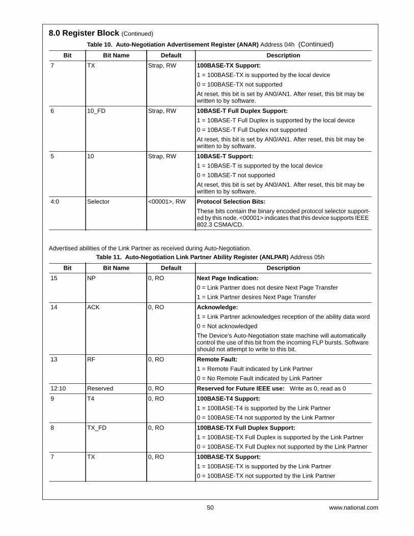
50 www.national.com
8.0 Register Block (Continued)
Advertised abilities of the Link Partner as received during Auto-Negotiation.
7 TX Strap, RW 100BASE-TX Support:
1 = 100BASE-TX is supported by the local device0 = 100BASE-TX not supportedAt reset, this bit is set by AN0/AN1. After reset, this bit may bewritten to by software.
6 10_FD Strap, RW 10BASE-T Full Duplex Support:
1 = 10BASE-T Full Duplex is supported by the local device0 = 10BASE-T Full Duplex not supportedAt reset, this bit is set by AN0/AN1. After reset, this bit may bewritten to by software.
5 10 Strap, RW 10BASE-T Support:
1 = 10BASE-T is supported by the local device0 = 10BASE-T not supportedAt reset, this bit is set by AN0/AN1. After reset, this bit may bewritten to by software.
4:0 Selector <00001>, RW Protocol Selection Bits:
These bits contain the binary encoded protocol selector support-ed by this node. <00001> indicates that this device supports IEEE802.3 CSMA/CD.
Table 11. Auto-Negotiation Link Partner Ability Register (ANLPAR) Address 05h
Bit Bit Name Default Description
15 NP 0, RO Next Page Indication:
0 = Link Partner does not desire Next Page Transfer1 = Link Partner desires Next Page Transfer
14 ACK 0, RO Acknowledge:
1 = Link Partner acknowledges reception of the ability data word0 = Not acknowledgedThe Device's Auto-Negotiation state machine will automaticallycontrol the use of this bit from the incoming FLP bursts. Softwareshould not attempt to write to this bit.
13 RF 0, RO Remote Fault:
1 = Remote Fault indicated by Link Partner0 = No Remote Fault indicated by Link Partner
12:10 Reserved 0, RO Reserved for Future IEEE use: Write as 0, read as 0
9 T4 0, RO 100BASE-T4 Support:
1 = 100BASE-T4 is supported by the Link Partner0 = 100BASE-T4 not supported by the Link Partner
8 TX_FD 0, RO 100BASE-TX Full Duplex Support:
1 = 100BASE-TX Full Duplex is supported by the Link Partner0 = 100BASE-TX Full Duplex not supported by the Link Partner
7 TX 0, RO 100BASE-TX Support:
1 = 100BASE-TX is supported by the Link Partner0 = 100BASE-TX not supported by the Link Partner
Table 10. Auto-Negotiation Advertisement Register (ANAR) Address 04h (Continued)Bit Bit Name Default Description

51 www.national.com
8.0 Register Block (Continued)
6 10_FD 0, RO 10BASE-T Full Duplex Support:
1 = 10BASE-T Full Duplex is supported by the Link Partner0 = 10BASE-T Full Duplex not supported by the Link Partner
5 10 0, RO 10BASE-T Support:
1 = 10BASE-T is supported by the Link Partner0 = 10BASE-T not supported by the Link Partner
4:0 Selector <00000>, RO Protocol Selection Bits:
Link Partners’s binary encoded protocol selector.
Table 11. Auto-Negotiation Link Partner Ability Register (ANLPAR) Address 05h
Bit Bit Name Default Description

52 www.national.com
8.0 Register Block (Continued)
This register also contains the Link Partner Next Page contents.
15 NP X RO Next Page Indication:
0 = Link Partner does not desire another Next Page Transfer1 = Link Partner desires another Next Page Transfer
14 ACK X, RO Acknowledge:
1 = Link Partner acknowledges reception of the ability data word0 = Not acknowledgedThe Device's Auto-Negotiation state machine will automaticallycontrol the use of this bit from the incoming FLP bursts. Softwareshould not attempt to write to this bit.
13 MP X, RO Message Page:
1 = Message Page0 = Unformatted Page
12 ACK2 X, RO Acknowledge 2:
0 = Link Partner does not have the ability to comply to next pagemessage1 = Link Partner has the ability to comply to next page message
11 TOGGLE X, RO Toggle:
0 = Previous value of the transmitted Link Code word equalledlogic one1 = Previous value of the transmitted Link Code word equalledlogic zero
10:0 CODE XXX, RW This field represents the code field of the next page transmission.If the MP bit is set (bit 13 of this register), then the code shall beinterpreted as a "Message Page," as defined in annex 28C ofClause 28. Otherwise, the code shall be interpreted as an "Un-formatted Page," and the interpretation is application specific.
Table 12. Auto-Negotiation Expansion Register (ANER) Address 06h
Bit Bit Name Default Description
15:5 Reserved 0, RO Reserved: Writes ignored, Read as 0.
4 PDF 0, RO Parallel Detection Fault:
1 = A fault has been detected via the Parallel Detection function0 = A fault has not been detected via the Parallel Detection func-tion
3 LP_NP_ABLE 0, RO Link Partner Next Page Able:
Status indicating if the Link Partner supports Next Page negotia-tion. A one indicates that the Link Partner does support NextPage.
2 NP_ABLE 1, RO/P Next Page Able:
Indicates if this node is able to send additional “Next Pages.”
1 PAGE_RX 0, RO/L Link Code Word Page Received:
This bit is set when a new Link Code Word Page has been re-ceived. Cleared on read of this register.
0 LP_AN_ABLE 0, RO Link Partner Auto-Negotiation Able:
A one in this bit indicates that the Link Partner supports Auto-Ne-gotiation.
Table 11. Auto-Negotiation Link Partner Ability Register (ANLPAR) Address 05h
Bit Bit Name Default Description

53 www.national.com
8.0 Register Block (Continued)
This register contains the next page information sent by this device to its Link Partner during Auto-Negotiation.Table 13. Auto-Negotiation Next Page Transmit Register (ANNPTR) Address 07h
Bit Bit Name Default Description
15 NP 0, RW Next Page Indication:
0 = No other Next Page Transfer desired1 = Another Next Page desired
14 Reserved 0, RO Reserved: Writes ignored, read as 0
13 MP 1, RW Message Page:
1 = Message Page0 = Unformatted Page
12 ACK2 0, RW Acknowledge2:
1 = Will comply with message0 = Cannot comply with messageAcknowledge2 is used by the next page function to indicate thata device has the ability to comply with the message received.
11 TOG_TX 1, RO Toggle:
1 = Previous value of transmitted Link Code Word equalled logic00 = Previous value of transmitted Link Code Word equalled logic1Toggle is used by the Arbitration function within Auto-Negotiationto ensure synchronization with the Link Partner during Next Pageexchange. This bit shall always take the opposite value of theToggle bit in the previously exchanged Link Code Word. The ini-tial value is the inverse of bit 11 in the base Link Code Word(ANAR), which makes the default value of TOG_TX = 1.
10:0 CODE 001, RW This field represents the code field of the next page transmission.If the MP bit is set (bit 13 of this register), then the code shall beinterpreted as a "Message Page," as defined in annex 28C ofClause 28. Otherwise, the code shall be interpreted as an "Un-formatted Page," and the interpretation is application specific.The default value of the CODE represents a Null Page as definedin annex 28C of Clause 28.

54 www.national.com
8.0 Register Block (Continued)
This register provides a single location within the register set for quick access to commonly accessed information.Table 14. PHY Status Register (PHYSTS) Address 10h
Bit Bit Name Default Description
15 Receive Error Latch 0, RO/L Receive Error Latch:
1 = Receive error event has occurred since last read of RXER-CNT0 = No receive error event has occurred
14 CIM Latch 0, RO/L Carrier Integrity Monitor Latch:
1 = Carrier Integrity Monitor has found an isolate event since lastread of DCR0 = No Carrier Integrity Monitor isolate event has occurred
13 False Carrier SenseLatch
0, RO/L False Carrier Sense Latch:
1 = False Carrier event has occurred since last read of FCSCR0 = No False Carrier event has occurred
12 Reserved 0, RO Reserved: Write ignored, read as 0.
11 Device Ready 0, RO Device Ready:
This bit signifies that the device is now ready to transmit data.1 = Device Ready0 = Device not Ready
10 Page Received 0, RO/L Link Code Word Page Received:
This bit is set when a new Link Code Word Page has been re-ceived. Cleared on read of the ANER register.
9 Auto-Negotiation En-abled
Strap, RO Auto-Negotiation Enabled:
1 = Auto-Negotiation Enabled.0 = Auto-Negotiation Disabled.
8 MII Interrupt 0, RO/L MII Interrupt Pending:
Indicates that an internal interrupt is pending and is cleared by thecurrent read. A read of this bit will clear the bit in the MIPGSR(12h) also.
7 Remote Fault 0, RO/L Remote Fault:
1 = Remote Fault condition detected (cleared on read of BMSRregister or by a chip reset). Fault criteria is Far end Fault Isolationor notification from Link Partner of Remote Fault.0 = No remote fault condition detected
6 Jabber Detect 0, RO/L Jabber Detect:
1 = Jabber condition detected0 = No JabberThis bit is implemented with a latching function so that the occur-rence of a jabber condition causes it to become set until it iscleared by a read to the BMSR register by the management inter-face or by a Device reset. This bit only has meaning in 10 Mb/smode.
5 NWAY Complete 0, RO Auto-Negotiation Complete:
1 = Auto-Negotiation complete0 = Auto-Negotiation not complete
4 Reset Status 0, RO Reset Status:
0 = Normal operation1 = Reset in progress

55 www.national.com
8.0 Register Block (Continued)
This register implements the MII Interrupt PHY Specific Control register. Sources for interrupt generation include: LinkState Change, Jabber Event, Remote Fault, Auto-Negotiation Complete or any of the counters becoming half-full. Notethat the TINT bit operates independently of the INTEN bit. In other words, INTEN does not need to be active to generatethe test interrupt.
This register implements the MII Interrupt PHY Generic Status Register.
3 Loopback Status 0, RO Loopback:
1 = Loopback enabled0 = Normal operation
2 Duplex Status RO Duplex:
This bit indicates duplex status and is determined from Auto-Ne-gotiation or Forced Modes.1 = Running in Full duplex mode0 = Running in Half duplex modeNote: This bit is only valid if Auto-Negotiation is enabled andcomplete and there is a valid link or if Auto-Negotiation is disabledand there is a valid link.
1 Speed Status RO Speed10:
This bit indicates the status of the speed and is determined fromAuto-Negotiation or Forced Modes.1 = Running in 10Mb/s mode0 = Running in 100 Mb/s modeNote: This bit is only valid if Auto-Negotiation is enabled andcomplete and there is a valid link or if Auto-Negotiation is disabledand there is a valid link.
0 Link Status 0, RO Link Status:
1 = Valid link established (for either 10 or 100 Mb/s operation)0 = Link not establishedThe criteria for link validity is implementation specific.
Table 15. MII Interrupt PHY Specific Control Register (MIPSCR) Address 11h
Bit Bit Name Default Description
15:2 Reserved 0, RO Reserved: Writes ignored, Read as 0
1 INTEN 0, RW Interrupt Enable:
1 = Enable event based interrupts0 = Disable event based interrupts
0 TINT 0, RW Test Interrupt:
Forces the PHY to always generate an interrupt to allow testingof the interrupt.1 = Generate an interrupt at the end of each access0 = Do not generate interrupt
Table 16. MII Interrupt PHY Generic Status Register (MIPGSR) Address 12h
Bit Bit Name Default Description
15 MINT 0, RO/COR MII Interrupt Pending:
Indicates that an interrupt is pending and is cleared by the currentread. A read of this will also clear the MII Interrupt bit (8) of thePHYSTS (10h) register.
14:0 Reserved 0, RO Reserved: Writes ignored, Read as 0
Table 14. PHY Status Register (PHYSTS) Address 10h (Continued)Bit Bit Name Default Description

56 www.national.com
8.0 Register Block (Continued)
This counter provides information required to implement the isolates attribute within the Repeater Port managed objectclass of Clause 30 of the IEEE 802.3 specification.
This counter provides information required to implement the FalseCarriers attribute within the MAU managed object classof Clause 30 of the IEEE 802.3 specification.
This counter provides information required to implement the aSymbolErrorDuringCarrier attribute within the PHY man-aged object class of Clause 30 of the IEEE 802.3 specification.
Table 17. Disconnect Counter Register (DCR) Address 13h
Bit Bit Name Default Description
15:0 DCNT[15:0] <0000h>, RW /COR
Disconnect Counter:
This 16 bit counter increments for each isolate event. Each timethe CIM detects a transition from the False Carrier state to theLink Unstable state of the Carrier Integrity State Machine, thecounter increments. This counter rolls over when it reaches itsmax count (FFFFh).
Table 18. False Carrier Sense Counter Register (FCSCR) Address 14h
Bit Bit Name Default Description
15:0 FCSCNT[15:0] <0000h>, RW /COR
False Carrier Event Counter:
This 16 bit counter increments for each false carrier event. A falsecarrier event occurs when carrier sense is asserted without J/Ksymbol detection. This counter rolls over when it reaches its maxcount (FFFFh).
Table 19. Receive Error Counter Register (RECR) Address 15h
Bit Bit Name Default Description
15:0 RXERCNT[15:0] <0000h>, RW /COR
RX_ER Counter:
This 16 bit counter is incremented for each receive error detect-ed. The counter is incremented when valid carrier is present andthere is at least one occurrence of an invalid data symbol. Thisevent can increment only once per valid carrier event. If a colli-sion is present, this attribute will not increment. This counter rollsover when it reaches its max count (FFFFh).
Table 20. 100 Mb/s PCS Configuration and Status Register (PCSR) Address 16h
Bit Bit Name Default Description
15 Single_SD 0, RW SIngle Ended Signal Detect Enable:
1=Single Ended SD mode enabled0=Single Ended SD mode disabled
14 FEFI_EN Strap, RW Far End Fault Indication Mode:
1 = FEFI mode enabled0 = FEFI mode disabledNote: If Auto-Negotiation is enabled, bit 12 of BMCR, this bit isRO and forced to zero. Additionally, if FX_EN is set to a one thenthis bit is RO and forced to a one.
13 DESCR_TO_RST 0, RW Reset Descrambler Time-Out Counter:
1 = Reset Time-Out Counter0 = Normal operation

57 www.national.com
8.0 Register Block (Continued)
12 DESCR_TO_SEL 0, RW Descrambler Time-out Select:
1 = Descrambler Timer set to 2 ms0 = Descrambler Timer set to 722 µsThe Descrambler Timer selects the interval over which a mini-mum number of IDLES are required to be received to maintaindescrambler synchronization. The default time of 722 µs sup-ports 100BASE-X compliant applications.A timer time-out indicates a loss of descrambler synchronizationwhich cause the descrambler to restart its operation by immedi-ately looking for IDLES.The 2 ms option allows applications with Maximum TransmissionUnits (packet sizes) larger than IEEE 802.3 to maintain descram-bler synchronization (i.e., Token Ring/Fast-Ethernet switch/rout-er applications).
11 DESCR_TO_DIS 0, RW Descrambler Time-out Disable:
1 = Time-out Counter in the descrambler section of the receiverdisabled0 = Time-out Counter enabled
10 LD_SCR_SD 0, RW Load Scrambler Seed:
1 = Load Scrambler Seed continuously0 = Normal operation
9 TX_QUIET 0, RW 100 Mps Transmit True Quiet Mode:
1 = Transmit True Quiet mode0 = Normal mode
8:7 TX_PATTERN[1:0] <00>, RW 100 Mps Transmit Test Pattern:
<00> = Normal operation<01> = Send FEFI pattern<10> = Send 1.28 µsperiod pattern (640 ns high/low time)<11> = Send 160 ns period pattern (80 ns high/low time)
6 F_LINK_100 0, RW Force Good Link in 100 Mb/s:
1 = Force 100 Mb/s Good Link status0 = Normal 100 Mb/s operationThis bit is useful for diagnostic purposes.
5 CIM_DIS Strap, RW Carrier Integrity Monitor Disable:
1 = Carrier Integrity Monitor function disabled (Node/Switch oper-ation)0 = Carrier Integrity Monitor function enabled (Repeater opera-tion)The THIN/REPEATER determines the default state of this bit toautomatically enable or disable the CIM function as required forIEEE 802.3 compliant applications. The value latched into this bitat power-on/reset is the compliment of the value forced on theTHIN/REPEATER input. After power-on/reset, software may en-able or disable this function independent of repeater ornode/switch mode.
Table 20. 100 Mb/s PCS Configuration and Status Register (PCSR) Address 16h (Continued)
Bit Bit Name Default Description

58 www.national.com
8.0 Register Block (Continued)
4 CIM_STATUS 0, RO Carrier Integrity Monitor Status:
This bit indicates the status of the Carrier Integrity Monitor func-tion. This status is optionally muxed out through the TX_LED pinwhen the LED_TXRX_MODE bits (8:7) of the PHYCTRL register(address 19h) are set to either <10> or <01>.1 = Unstable link condition detected0 = Unstable link condition not detected
3 CODE_ERR 0, RW Code Errors:
1 = Forces code errors to be reported with the value 5h onRXD[3:0] and with RX_ER set to 1.0 = Forces code errors to be reported with the value of 6h onRXD[3:0] and with RX_ER set to 1.
2 PME_ERR 0, RW Premature End Errors:
1 = Forces premature end errors to be reported with the value 4hon RXD[3:0] and with RX_ER set to 1.0 = Forces premature end errors to be reported with the value 6hon RXD[3:0] and with RX_ER set to 1. Premature end errors arecaused by the detection of two IDLE symbols in the receive datastream prior to the T/R symbol pair denoting end of stream delim-iter.
1 LINK_ERR 0, RW Link Errors:
1 = Forces link errors to be reported with the value 3h onRXD[3:0] and with RX_ER set to 1.0 = Data is passed to RXD[3:0] unchanged and with RX_ER setto 0.
0 PKT_ERR 0, RW Packet Errors:
1 = Forces packet errors (722 s time-out) to be reported with thevalue 2h on RXD[3:0] and with RX_ER set to 1.0 = Data is passed to RXD[3:0] unchanged and with RX_ER setto 0.
Table 21. Loopback & Bypass Register (LBR) Address 17h
Bit Bit Name Default Description
15 Reserved 0, RO Reserved: Writes ignored, read as 0.
14 BP_STRETCH 0, RW Bypass LED Stretching:
This will bypass the LED stretching and the LEDs will reflect theinternal value.1 = Bypass LED stretching0 = Normal operation
13 BP_4B5B Strap, RW Bypass 4B5B Encoding and 5B4B Decoding:
This bit is set according to the strap configuration of the SYMBOLpin at power-up/reset. After reset this bit may be written to by soft-ware.1 = 4B5B encoder and 5B4B decoder functions bypassed0 = Normal 4B5B and 5B4B operation
Table 20. 100 Mb/s PCS Configuration and Status Register (PCSR) Address 16h (Continued)
Bit Bit Name Default Description

59 www.national.com
8.0 Register Block (Continued)
12 BP_SCR Strap, RW Bypass Scrambler/Descrambler Function:
This bit is set according to the strap configuration of the SYMBOLpin or the FXEN pin at power-up/reset. After reset this bit may bewritten to by software.1 = Scrambler and descrambler functions bypassed0 = Normal scrambler and descrambler operation
11 BP_RX Strap, RW Bypass Receive Function:
This bit is set according to the strap configuration of the SYMBOLpin at power-up/reset. After reset this bit may be written to by soft-ware.1 = Receive functions (descrambler and symbol decoding func-tions) bypassed.0 = Normal operation.
10 BP_TX Strap, RW Bypass Transmit Function:
This bit is set according to the strap configuration of the SYMBOLpin at power-up/reset. After reset this bit may be written by soft-ware.1 = Transmit functions (symbol encoder and scrambler) by-passed0 = Normal operation
9:7 100_DP_CTL Strap, RW 100Mps Data Path Control Bits:
At reset, if FXEN is true then this will default to <011>, else it willdefault to <000>. These bits control the 100Mps loopback func-tion in CorePhy as follows:<000> Normal Mode<001> CorePhy Loopback<010> Reserved<011> Normal Fiber<100> Reserved<101> Reserved<110> Reserved<111> ReservedNote: A write to the Loopback bit (14) of the BMCR (00h) willoverride the value set in this register.
6 RESERVED 0, RO Reserved: Writes as 0, read as 0
5 TW_LBEN 0, RW TWISTER Loopback Enable:
1 = TWISTER loopback0 = Normal modeNote: A write to the Loopback bit (14) of the BMCR (00h) willoverride the value set in this register.
4 10Mb_ENDEC_LB 0, RW 10 Mb/s ENDEC Loopback:
1 = 10Mb/s ENDEC loopback0 = Normal TREX operationNote: A write to the Loopback bit (14) of the BMCR (00h) willoverride the value set in this register.
3 RESERVED 0, RO Reserved: Writes as 0, read as 0
2 RESERVED 0, RO Reserved: Writes as 0, read as 0
Table 21. Loopback & Bypass Register (LBR) Address 17h (Continued)
Bit Bit Name Default Description

60 www.national.com
8.0 Register Block (Continued)
1 RESERVED 0, RO Reserved: Writes as 0, read as 0
0 RESERVED 0, RO Reserved: Writes as 0, read as 0
Table 22. 10BASE-T Control & Status Register (10BTSCR) Address 18h
Bit Bit Name Default Description
15:14 RESERVED 0, RO Reserved: Writes ignored, read as 0
13 AUI_TPI 0, RO TREX Operating Mode:
This bit shows the current operating mode of TREX as chosen bythe Auto-Switch function.1 = AUI mode0 = TPI mode
12 RX_SERIAL Strap, RW 10BASE-T RX Serial Mode:
This bit is set according to the strap configuration of theSERIAL10 pin at power-up/reset. After reset this bit may be writ-ten to by software.1 = 10BASE-T rx Serial mode selected0 = 10BASE-T rx Nibble mode selectedSerial mode is not supported for 100 Mb/s operation.
11 TX_SERIAL Strap, RW 10BASE-T TX Serial Mode:
This bit is set according to the strap configuration of theSERIAL_10 pin at power-up/reset. After reset this bit may be writ-ten to by software.1 = 10BASE-T tx Serial mode selected0 = 10BASE-T tx Nibble mode selectedSerial mode is not supported for 100 Mb/s operation.
10 POL_DS 0, RW Polarity Detection & Correction Disable:
1 = Polarity Sense & Correction disabled0 = Polarity Sense & Correction enabled
9 AUTOSW_EN 0, RW AUI/TPI Autoswitch:
1 = Enable autoswitch0 = Disable autoswitch functionThe use of autoswitch should be strictly limited to applicationsthat do not support Auto-Negotiation. Do not enable Auto-Nego-tiation when enabling autoswitch as this may result in improperoperation.
8 LP_DS 0, RW Link Pulse Disable:
1 = Reception of link pulses ignored, good link condition forced0 = Good link not forced, link pulses observed for good link
7 HB_DS 0, RW Heartbeat Disable:
1 = Heartbeat function disabled0 = Heartbeat function enabledWhen the device is configured for full duplex operation, this bit willbe ignored (the collision/heartbeat function has no meaning inFull Duplex mode). HB_DS will read back as 1 if in Full Duplexmode or Repeater mode.
Table 21. Loopback & Bypass Register (LBR) Address 17h (Continued)
Bit Bit Name Default Description

61 www.national.com
8.0 Register Block (Continued)
6 LS_SEL 0, RW Low Squelch Select:
Selects between standard 10BASE-T receiver squelch thresholdand a reduced squelch threshold that is useful for longer cableapplications.1 = Low Squelch Threshold selected0 = Normal 10BASE-T Squelch Threshold selected
5 AUI_SEL 0, RW AUI Select:
1 = Select AUI interface0 = Select TPI interface
4 JAB_DS 0, RW Jabber Disable:
Enables or disables the Jabber function when the device is in10BASE-T Full Duplex or 10BASE-T TREX Loopback mode(TREX_LBEN bit 4 in the LBR, address 17h).1 = Jabber function disabled0 = Jabber function enabled
3 THIN_SEL 0, RW Thin Ethernet Select:
1 = Asserts THIN pin (pin 63)0 = Deasserts THIN pin (pin 63)This pin may be used as a general purpose select pin.
2 RX_FILT_DS 0, RW TPI Receive Filter Disable:
1 = Disable TPI receive filter0 = Enable TPI receive filter
1 RESERVED 0, RO Reserved: Writes ignored, read as 0
0 RESERVED 0, RO Reserved: Writes as 0, read as 0
Table 23. PHY Control Register (PHYCTRL) Address 19h
Bit Bit Name Default Description
15 RESERVED 0, RO Reserved: Writes ignored, read as 0
14 RESERVED 0, RO Reserved: Writes ignored, read as 0
13:12 TW_EQSEL[1:0] <00>, RW TWISTER Equalization Select:
Used in combination to select the 4 equalization modes. Modes3, 2, 1 should be accessible to external device pin for debug pur-poses.<11> = Equalization off<10> = Equalization on<01> = Adaptive Equalization<00> = Full Adaptive Equalization
11 TW_BLW_DS 0, RW TWISTER Base Line Wander Disable:
1 = BLW Feedback loop disabled0 = BLW Feedback loop enabled
10 RESERVED 0, RO Reserved: Writes ignored, read as 0
Table 22. 10BASE-T Control & Status Register (10BTSCR) Address 18h (Continued)
Bit Bit Name Default Description
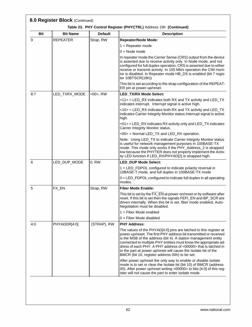
62 www.national.com
8.0 Register Block (Continued)
9 REPEATER Strap, RW Repeater/Node Mode:
1 = Repeater mode0 = Node modeIn repeater mode the Carrier Sense (CRS) output from the deviceis asserted due to receive activity only. In Node mode, and notconfigured for full duplex operation, CRS is asserted due to eitherreceive or transmit activity. In 100 Mb/s operation the CIM moni-tor is disabled. In Repeater mode HB_DS is enabled (bit 7 regis-ter 10BTSCR(18h))This bit is set according to the strap configuration of the REPEAT-ER pin at power-up/reset.
8:7 LED_TXRX_MODE <00>, RW LED_TX/RX Mode Select:
<11> = LED_RX indicates both RX and TX activity and LED_TXindicates interrupt. Interrupt signal is active high.<10> = LED_RX indicates both RX and TX activity and LED_TXindicates Carrier Integrity Monitor status.Interrupt signal is activehigh.<01> = LED_RX indicates RX activity only and LED_TX indicatesCarrier Integrity Monitor status.<00> = Normal LED_TX and LED_RX operation.Note: Using LED_TX to indicate Carrier Integrity Monitor statusis useful for network management purposes in 100BASE-TXmode. This mode only works if the PHY_Address_2 is strappedlow because the PHYTER does not properly implement the Activ-ity LED function if LED_RX/PHYAD[2] is strapped high.
6 LED_DUP_MODE 0, RW LED_DUP Mode Select:
1 = LED_FDPOL configured to indicate polarity reversal in10BASE-T mode, and full duplex in 100BASE-TX mode0 = LED_FDPOL configured to indicate full duplex in all operatingmodes.
5 FX_EN Strap, RW Fiber Mode Enable:
This bit is set by the FX_EN at power-on/reset or by software afterreset. If this bit is set then the signals FEFI_EN and BP_SCR aredriven internally. When this bit is set, fiber mode enabled, Auto-Negotiation must be disabled.1 = Fiber Mode enabled0 = Fiber Mode disabled
4:0 PHYADDR[4:0] (STRAP), RW PHY Address:
The values of the PHYAD[4:0] pins are latched to this register atpower-up/reset. The first PHY address bit transmitted or receivedis the MSB of the address (bit 4). A station management entityconnected to multiple PHY entities must know the appropriate ad-dress of each PHY. A PHY address of <00000> that is latched into the part at power up/reset will cause the Isolate bit of theBMCR (bit 10, register address 00h) to be set.After power up/reset the only way to enable or disable isolatemode is to set or clear the Isolate bit (bit 10) of BMCR (address00). After power up/reset writing <00000> to bits [4:0] of this reg-ister will not cause the part to enter isolate mode.
Table 23. PHY Control Register (PHYCTRL) Address 19h (Continued)
Bit Bit Name Default Description

63 www.national.com
Absolute Maximum Ratings
Supply Voltage (VCC) -0.5 V to 7.0 VInput Voltage (DCIN) -0.5 V to VCC + 0.5 VOutput Voltage (DCOUT) -0.5 V to VCC + 0.5 VStorage Temperature -65oC to 150oCECL Signal Output Current -50mAESD Protection 2000 V
Recommended Operating Conditions
Min Typ Max UnitsSupply voltage (VDD) 4.75 5.0 5.25 VAmbient Temperature (TA) 0 70 oCX1 Input Frequency Stability(over temperature)
-50 +50 PPM
X1 Input Duty Cycle 35 65 %Center Frequency (XFC) 25 MHz
9.0 Electrical Specifications
All preliminary electrical specifications are based on IEEE 802.3u requirements and internal design considerations.These specifications will not become final until complete verification of the DP83843.Thermal Characteristics*
*Valid for Phyters with data code 9812 or later, for earlier data codes please contact your National Sales Representative for data.
Max UnitsMaximum Case Temperature 96 oCMaximum Die Temperature 104.7 oCTheta Junction to Case (Tjc) 1.1 oC / WTheta Junction to Ambient (Tja) degrees Celsius/Watt - No Airflow @ 1.0W 42.7 oC / WTheta Junction to Ambient (Tja) degrees Celsius/Watt - 225 LFPM Airflow @ 1.0W 35.3 oC / WTheta Junction to Ambient (Tja) degrees Celsius/Watt - 500 LFPM Airflow @ 1.0W 30.4 oC / WTheta Junction to Ambient (Tja) degrees Celsius/Watt - 900 LFPM Airflow @ 1.0W 26.9 oC / W

9.0 Electrical Specifications (Continued)
64 www.national.com
9.1 DC Electrical Specification
Symbol Pin Types Parameter Conditions Min Typ Max Units
VIH II/O
I/O, Z
Input High Voltage 2.0 V
AN0 and AN1 VCC - 1.0 V
X1 VCC - 1.0 V
VIL II/O
I/O, Z
Input Low Voltage 0.8 V
AN0 and AN1 1.0 V
X1 1.0 V
VIM AN0 and AN1 Input Mid LevelVoltage
Pin Unconnected (VCC/2)-0.5
(VCC/2) (VCC/2)+0.5
V
IIH II/O
I/O, Z
Input High Current VIN = VCC 10 µA
X1 X2 = N.C. -100 µA
IIL II/O
I/O, Z
Input Low Current VIN = GND 10 µA
X1 X2 = N.C. 100 µA
VOL O, ZI/O
I/O, Z
Output LowVoltage
IOL = 4 mA 0.4 V
VOH O, ZI/O
I/O, Z
Output HighVoltage
IOL = -4 mA VCC - 0.5 V
VOL LEDSPEED10
Output LowVoltage
IOL = 2.5 mA 0.4 V
VOH LEDSPEED10
Output HighVoltage
IOL = -2.5 mA VCC - 0.5 V
IOZ1 I/O, ZO, Z
TRI-STATELeakage
VOUT = VCC 10 µA
IOZ2 I/O, ZO, Z
TRI-STATELeakage
VOUT = GND -10 µA
RINdiff TPRD+/− Differential InputResistance
see TestConditions section
5 6 kΩ
VTPTD_100 TPTD+/− 100M TransmitVoltage
see TestConditionssection
.95 1 1.05 V
VTPTDsym TPTD+/− 100M TransmitVoltage Symmetry
see TestConditions section
-2 +2 %
VTPTD_10 TPTD+/− 10M TransmitVoltage
see TestConditions section
2.2 2.5 2.8 V
CIN1 I CMOS InputCapacitance
8 pF
CIN2 I PECL InputCapacitance
10 pF

9.0 Electrical Specifications (Continued)
65 www.national.com
COUT1 OZ
CMOS OutputCapacitance
8 pF
COUT2 OZ
PECL OutputCapacitance
10 pF
SDTHon TPRD+/− 100BASE-TXSignal detect turn-on thresh
1000 mV diff pk-pk
SDTHoff TPRD+/− 100BASE-TXSignal detect turn-off thresh
200 mV diff pk-pk
VTH1 TPRD+/− 10BASE-T Re-ceive Threshold
300 585 mV
VTH2 TPRD+/− 10BASE-T Re-ceive LowSquelch Thresh-old
150 300 mV
VDIFF FXSD+/−,FXRD+/−
PECL Input Volt-age Differential
see TestConditions section
300 mV
VCM FXSD+/−,FXRD+/−
PECL CommonMode Voltage
see TestConditions section
VCC - 2.0 VCC - 0.5 mV
IINECL FXSD+/−,FXRD+/−
PECL InputCurrent
VIN = VOLmax or
VOHmax
-300 300 µA
VOHECL FXTD+/− PECL Output HighVoltage
VIN = VIHmax VCC - 1.125 VCC - 0.78 V
VOLECL FXTD+/− PECL Output LowVoltage
VIN = VILmax VCC - 1.86 VCC - 1.515 V
VODaui AUITD+/− Differential OutputVoltage
see TestConditions section
± 550 ± 1200 mV
VOBaui AUITD+/− Differential IdleOutput VoltageImbalance
see TestConditions section
40 mV
VDSaui AUIRD+/−,AUICD+/−
DifferentialSquelchThreshold
see TestConditions section
± 160 ± 300 mV
Idd100 Supply 100BASE-TX(Full Duplex)
see TestConditions section
135 150 mA
Idd10 Supply 10BASE-TX(Full Duplex)
see TestConditions section
100 110 mA
IddFX Supply 100BASE-FX(Full Duplex)
see TestConditions section
100 115 mA
IddAN Supply Auto-Negotiation see TestConditions section
100 120 mA
IddPD Supply Power Down see TestConditions section
25 30 mA
Symbol Pin Types Parameter Conditions Min Typ Max Units
9.0 Electrical Specifications (Continued)
66 www.national.com
9.2 CGM Clock Timing
9.3 MII Serial Management AC Timing
Parameter Description Notes Min Typ Max Units
T2.0.1 X1 to TX_CLK Delay -3 +3 ns
T2.0.2 TX_CLK Duty Cycle 35 65 %
Parameter Description Notes Min Typ Max Units
T3.0.1 MDC to MDIO (Output) Delay Time 0 300 ns
T3.0.2 MDIO (Input) to MDC Setup Time 10 ns
T3.0.3 MDIO (Input) to MDC Hold Time 10 ns
T3.0.4 MDC Frequency 2.5 MHz
TX_CLK OUT
X1 IN
T2.0.1T2.0.2
MDC
MDC
MDIO (OUTPUT)
MDIO (INPUT) VALID DATA
T3.0.1
T3.0.2 T3.0.3
T3.0.4

9.0 Electrical Specifications (Continued)
67 www.national.com
9.4 100 Mb/s AC Timing9.4.1 100 Mb/s MII Transmit Timing
9.4.2 100 Mb/s MII Receive Timing
Parameter Description Notes Min Typ Max Units
T4.1.1 TXD[3:0], TX_EN, TX_ER Data Setup toTX_CLK
100 Mb/s Normal mode 14 ns
TXD[4:0] Data Setup to TX_CLK 100 Mb/s Symbol mode 10 ns
T4.1.2 TXD[3:0], TX_EN, TX_ER Data Hold fromTX_CLK
100 Mb/s Normal mode -1 ns
TXD[4:0] Data Hold from TX_CLK 100 Mb/s Symbol mode -1 ns
Parameter Description Notes Min Typ Max Units
T4.2.1 RX_EN to RX_CLK, RXD[3:0], RX_ER,RX_DV Active
All 100 Mb/s modes 15 ns
T4.2.2 RX_EN to RX_CLK, RXD[3:0], RX_ER,RX_DV TRI-STATE
All 100 Mb/s modes 25 ns
T4.2.3 RX_CLK to RXD[3:0], RX_DV, RX_ER Delay 100 Mb/s Normal mode 10 30 ns
RX_CLK to RXD[4:0], Delay 100 Mb/s Symbol mode 10 30 ns
T4.2.4 RX_CLK Duty Cycle All 100 Mb/s modes 35 65 %
TX_CLK
TXD[3:0]TX_ENTX_ER
VALID DATA
T4.1.1 T4.1.2
RX_CLK
RXD[3:0]RX_DVRX_ER VALID DATA
RX_ENT4.2.1 T4.2.2
T4.2.3
T4.2.4

9.0 Electrical Specifications (Continued)
68 www.national.com
9.4.3 100BASE-TX Transmit Packet Latency Timing
Note: For Normal mode, latency is determined by measuring the time from the first rising edge of TX_CLK occurring after the assertion of TX_EN to the firstbit of the “j” code group as output from the TPTD± pins. 1 bit time = 10ns in 100 Mb/s mode. For Symbol mode, because TX_EN has no meaning, latencyis measured from the first rising edge of TX_CLK occurring after the assertion of a data nibble on the Transmit MII to the first bit (MSB) of that nibble asoutput from the TPTD± pins. 1 bit time = 10 ns in 100 Mb/s mode.
Parameter Description Notes Min Typ Max Units
T4.3.1 TX_CLK to TPTD+/− Latency 100 Mb/s Normal mode 6.0 bits
100 Mb/s Symbol mode 6.0 bits
TX_CLK
TX_EN
TXD
TPTD+/-(J/K) IDLE DATA
T4.3.1

9.0 Electrical Specifications (Continued)
69 www.national.com
9.4.4 100BASE-TX Transmit Packet Deassertion Timing
Note: Deassertion is determined by measuring the time from the first rising edge of TX_CLK occurring after the deassertion of TX_EN to the first bit of the“T” code group as output from the TPTD± pins. For Symbol mode, because TX_EN has no meaning, Deassertion is measured from the first rising edge ofTX_CLK occurring after the deassertion of a data nibble on the Transmit MII to the last bit (LSB) of that nibble when it deasserts on the wire. 1 bit time = 10ns in 100 Mb/s mode.
Parameter Description Notes Min Typ Max Units
T4.4.1 TX_CLK to TPTD+/−Deassertion
100 Mb/s Normal mode 6.0 bits
100 Mb/s Symbol mode 6.0 bits
TX_CLK
TX_EN
TXD
TPTD+/-(T/R)DATA IDLE
T4.4.1

9.0 Electrical Specifications (Continued)
70 www.national.com
9.4.5 100BASE-TX Transmit Timing
Note: Normal Mismatch is the difference between the maximum and minimum of all rise and fall times.
Note: Rise and fall times taken at 10% and 90% of the +1 or -1 amplitude.
Parameter Description Notes Min Typ Max Units
T4.5.1 100 Mb/s TPTD+/− Rise andFall Times
see Test Conditions section 3 4 5 ns
100 Mb/s Rise/Fall Mismatch 500 ps
T4.5.2 100 Mb/s TPTD+/−Transmit Jitter
1.4 ns
TPTD+/-
T4.5.1 T4.5.1T4.5.1T4.5.1
+1 RISE +1 FALL -1 FALL -1 RISE
TPTD+/-EYE PATTERN
T4.5.2
T4.5.2

9.0 Electrical Specifications (Continued)
71 www.national.com
9.4.6 100BASE-TX Receive Packet Latency Timing
Note: Carrier Sense On Delay is determined by measuring the time from the first bit of the “J” code group to the assertion of Carrier Sense.
Note: 1 bit time = 10 ns in 100 Mb/s mode.
Note: TPRD± voltage amplitude is greater than the Signal Detect Turn-On Threshold Value.
9.4.7 100BASE-TX Receive Packet Deassertion Timing
Note: Carrier Sense Off Delay is determined by measuring the time from the first bit of the “T” code group to the deassertion of Carrier Sense.
Note: 1 bit time = 10 ns in 100 Mb/s mode.
Parameter Description Notes Min Typ Max Units
T4.6.1 Carrier Sense on Delay 100 Mb/s Normal mode 17.5 bits
T4.6.2 Receive Data Latency 100 Mb/s Normal mode 21 bits
100 Mb/s Symbol mode 12 bits
Parameter Description Notes Min Typ Max Units
T4.7.1 Carrier Sense Off Delay 100 Mb/s Normal mode 21.5 bits
CRS
RXD[3:0]
TPRD+/-
RX_DVRX_ER/RXD[4]
(J/K)IDLE DATA
T4.6.1
T4.6.2
CRS
TPRD+/- (T/R) IDLEDATA
T4.7.1
RXD[3:0]RX_DV
RX_ER/RXD[4]

9.0 Electrical Specifications (Continued)
72 www.national.com
9.4.8 100BASE-FX Transmit Packet Latency Timing
Note: For Normal mode, Latency is determined by measuring the time from the first rising edge of TX_CLK occurring after the assertion of TX_EN to thefirst bit of the “j” code group as output from the FXTD± pins. For Symbol mode, because TX_EN has no meaning, Latency is measured from the first risingedge of TX_CLK occurring after the assertion of a data nibble on the Transmit MII to the first bit (MSB) of that nibble when it first appears at the FXTD±outputs.
Parameter Description Notes Min Typ Max Units
T4.8.1 TX_CLK to FXTD+/− Latency 100 Mb/s Normal mode 4.0 bits
100 Mb/s Symbol mode 4.0 bits
TX_CLK
TX_EN
TXD
FXTD+/-(J/K) IDLE DATA
T4.8.1
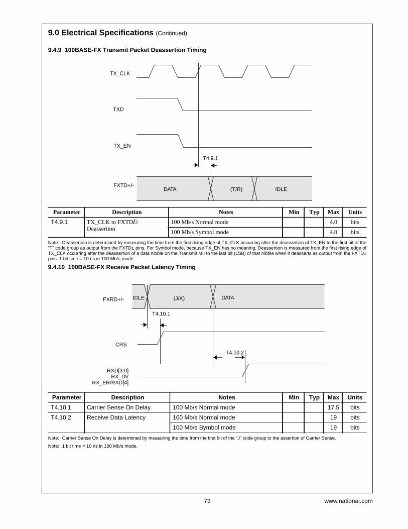
9.0 Electrical Specifications (Continued)
73 www.national.com
9.4.9 100BASE-FX Transmit Packet Deassertion Timing
Note: Deassertion is determined by measuring the time from the first rising edge of TX_CLK occurring after the deassertion of TX_EN to the first bit of the“T” code group as output from the FXTD± pins. For Symbol mode, because TX_EN has no meaning, Deassertion is measured from the first rising edge ofTX_CLK occurring after the deassertion of a data nibble on the Transmit MII to the last bit (LSB) of that nibble when it deasserts as output from the FXTD±pins. 1 bit time = 10 ns in 100 Mb/s mode.
9.4.10 100BASE-FX Receive Packet Latency Timing
Note: Carrier Sense On Delay is determined by measuring the time from the first bit of the “J” code group to the assertion of Carrier Sense.
Note: 1 bit time = 10 ns in 100 Mb/s mode.
Parameter Description Notes Min Typ Max Units
T4.9.1 TX_CLK to FXTD+/−Deassertion
100 Mb/s Normal mode 4.0 bits
100 Mb/s Symbol mode 4.0 bits
Parameter Description Notes Min Typ Max Units
T4.10.1 Carrier Sense On Delay 100 Mb/s Normal mode 17.5 bits
T4.10.2 Receive Data Latency 100 Mb/s Normal mode 19 bits
100 Mb/s Symbol mode 19 bits
TX_CLK
TX_EN
TXD
FXTD+/-(T/R)DATA IDLE
T4.9.1
CRS
RXD[3:0]
FXRD+/-
RX_DVRX_ER/RXD[4]
(J/K)IDLE DATA
T4.10.2
T4.10.1
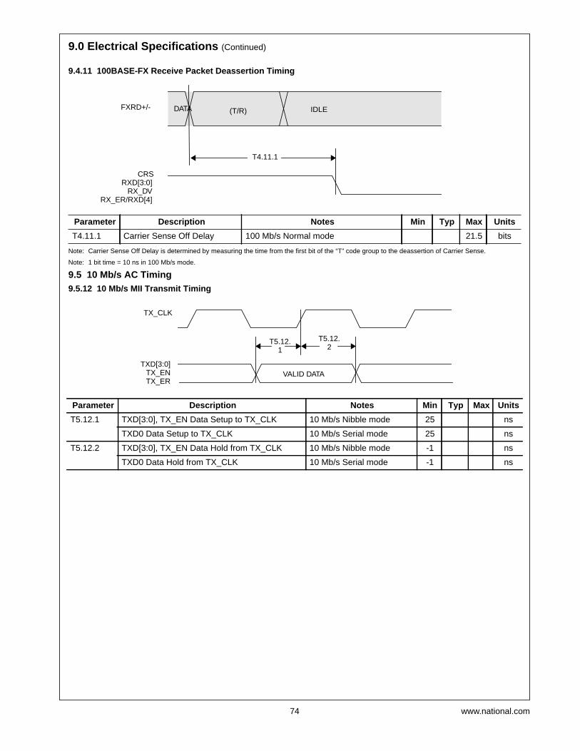
9.0 Electrical Specifications (Continued)
74 www.national.com
9.4.11 100BASE-FX Receive Packet Deassertion Timing
Note: Carrier Sense Off Delay is determined by measuring the time from the first bit of the “T” code group to the deassertion of Carrier Sense.
Note: 1 bit time = 10 ns in 100 Mb/s mode.
9.5 10 Mb/s AC Timing9.5.12 10 Mb/s MII Transmit Timing
Parameter Description Notes Min Typ Max Units
T4.11.1 Carrier Sense Off Delay 100 Mb/s Normal mode 21.5 bits
Parameter Description Notes Min Typ Max Units
T5.12.1 TXD[3:0], TX_EN Data Setup to TX_CLK 10 Mb/s Nibble mode 25 ns
TXD0 Data Setup to TX_CLK 10 Mb/s Serial mode 25 ns
T5.12.2 TXD[3:0], TX_EN Data Hold from TX_CLK 10 Mb/s Nibble mode -1 ns
TXD0 Data Hold from TX_CLK 10 Mb/s Serial mode -1 ns
CRS
FXRD+/- (T/R) IDLEDATA
T4.11.1
RXD[3:0]RX_DV
RX_ER/RXD[4]
TX_CLK
TXD[3:0]TX_ENTX_ER
VALID DATA
T5.12.1
T5.12.2

9.0 Electrical Specifications (Continued)
75 www.national.com
9.5.13 10 Mb/s MII Receive Timing
9.5.14 10BASE-T Transmit Timing (Start of Packet)
Note: 1 bit time = 100 ns in 10 Mb/s mode for both nibble and serial operation.
Parameter Description Notes Min Typ Max Units
T5.13.1 RX_EN to RX_CLK, RXD[3:0], RX_DV Active All 10 Mb/s modes 10 ns
T5.13.2 RX_EN to RX_CLK, RXD[3:0], RX_DV TRI-STATE
All 10 Mb/s modes 25 ns
T5.13.3 RX_CLK to RXD[3:0], RX_DV, RX_ER Delay 10 Mb/s Nibble mode 190 210 ns
RX_CLK to RXD[3:0], RX_DV, RX_ER Delay 10 Mb/s Serial mode 40 60 ns
T5.13.4 RX_CLK Duty Cycle All 10 Mb/s modes 35 65 %
Parameter Description Notes Min Typ Max Units
T5.14.1 Transmit Enable Setup Time from theRising Edge of TX_CLK
10 Mb/s Nibble mode 25 ns
10 Mb/s Serial mode 25 ns
T5.14.2 Transmit Data Setup Time from theRising Edge of TX_CLK
10 Mb/s Nibble mode 25 ns
10 Mb/s Serial mode 25 ns
T5.14.3 Transmit Data Hold Time from theRising Edge of TX_CLK
10 Mb/s Nibble mode -1 ns
10 Mb/s Serial mode -1 ns
T5.14.4 Transmit Output Delay from theRising Edge of TX_CLK
10 Mb/s Nibble mode 6.8 bits
10 Mb/s Serial mode 2.5 bits
RX_CLK
RXD[3:0]RX_DVRX_ER VALID DATA
RX_ENT5.13.1 T5.13.
2
T5.13.3
T5.13.4
TX_CLK
TX_EN
TXD
TPTD+/-
T5.14.1
T5.14.2 T5.14.3
T5.14.4

9.0 Electrical Specifications (Continued)
76 www.national.com
9.5.15 10BASE-T Transmit Timing (End of Packet)
Parameter Description Notes Min Typ Max Units
T5.15.1 Transmit Enable Hold Time from theRising Edge of TX_CLK
10 Mb/s Nibble mode -1 ns
10 Mb/s Serial mode -1 ns
T5.15.2 End of Packet High Time(with ‘0’ ending bit)
10 Mb/s Nibble mode 250 ns
10 Mb/s Serial mode 250 ns
T5.15.3 End of Packet High Time(with ‘1’ ending bit)
10 Mb/s Nibble mode 250 ns
10 Mb/s Serial mode 250 ns
TX_CLK
TX_EN
TPTD+/-0 0
1 1TPTD+/-
T5.15.2
T5.15.3
T5.15.1

9.0 Electrical Specifications (Continued)
77 www.national.com
9.5.16 10BASE-T Receive Timing (Start of Packet)
Note: 10BASE-T receive Data Latency is measured from first bit of preamble on the wire to the assertion of RX_DV.
Note: 1 bit time = 100 ns in 10 Mb/s mode for both nibble and serial operation.
9.5.17 10BASE-T Receive Timing (End of Packet)
Parameter Description Notes Min Typ Max Units
T5.16.1 Carrier Sense Turn On Delay(TPRD+/− to CRS)
10 Mb/s Nibble mode 1 µs
10 Mb/s Serial mode 1 µs
T5.16.2 Decoder Acquisition Time 10 Mb/s Nibble mode 3.6 µs
10 Mb/s Serial mode 3.2 µs
T5.16.3 Receive Data Latency 10 Mb/s Nibble mode 17.3 bits
10 Mb/s Serial mode 10 bits
T5.16.4 SFD Propagation Delay 10 Mb/s Nibble mode 10 bits
10 Mb/s Serial mode 4.5 bits
Parameter Description Notes Min Typ Max Units
T5.17.1 Carrier Sense Turn Off Delay 10 Mb/s Nibble mode 1.1 us
10 Mb/s Serial mode 450 ns
1 0 1
TPRD+/-
CRS
RX_CLK
RXD
1ST SFD BIT DECODED
RX_DV
T5.16.1
T5.16.
T5.16.
T5.16.4
1 0 1
TPRD+/-
RX_CLK
CRS
IDLE
T5.17.1

9.0 Electrical Specifications (Continued)
78 www.national.com
9.5.18 10 Mb/s AUI Timing
Note: The worst case for T5.18.1 is data ending in a ‘0’.
9.5.19 10 Mb/sHeartbeat Timing
Parameter Description Notes Min Typ Max Units
T5.18.1 AUI Transmit Output High BeforeIdle
200 ns
T5.18.2 AUI Transmit Output Idle Time 8000 ns
T5.18.3 AUI Receive End of Packet HoldTime
225 ns
Parameter Description Notes Min Typ Max Units
T5.19.1 CD Heartbeat Delay 10 Mb/s Nibble mode 700 ns
10 Mb/s Serial mode 700 ns
T5.19.2 CD Heartbeat Duration 10 Mb/s Nibble mode 700 ns
10 Mb/s Serial mode 700 ns
1 0
AUITD+/-
0
T5.18.AUIRD+/-
T5.18.
T5.18.
TXC
TXE
COL
T5.19. T5.19.

9.0 Electrical Specifications (Continued)
79 www.national.com
9.5.20 10 Mb/s Jabber Timing
9.5.21 10BASE-T Normal Link Pulse Timing
Note: These specifications represent both transmit and receive timings.
Parameter Description Notes Min Typ Max Units
T5.20.1 Jabber Activation Time 10 Mb/s Nibble mode 26 ms
10 Mb/s Serial mode 26 ms
T5.20.2 Jabber Deactivation Time 10 Mb/s Nibble mode 500 ms
10 Mb/s Serial mode 500 ms
Parameter Description Notes Min Typ Max Units
T5.21.1 Pulse Width 100 ns
T5.21.2 Pulse Period 8 16 24 ms
TXE
TPTD+/-
COL
T5.20.T5.20.1
T5.21.2
T5.21.1

9.0 Electrical Specifications (Continued)
80 www.national.com
9.6 Auto-Negotiation Fast Link Pulse (FLP) Timing
Note: These specifications represent both transmit and receive timings.
9.7 100BASE-X Clock Recovery Module (CRM) Timing
Note: The Ideal window recognition region is ± 4 ns.
Parameter Description Notes Min Typ Max Units
T6.21.1 Clock, Data Pulse Width 100 ns
T6.21.2 Clock Pulse to Clock PulsePeriod
111 125 139 µs
T6.21.3 Clock Pulse to Data PulsePeriod
Data = 1 55.5 69.5 µs
T6.21.4 Number of Pulses in a Burst 17 33 #
T6.21.5 Burst Width 2 ms
T6.21.6 FLP Burst to FLP Burst Period 8 24 ms
Parameter Description Notes Min Typ Max Units
T7.21.1 CRM Window Recognition Region -2.7 2.7 ns
CLOCKPULSE
DATAPULSE
CLOCKPULSE
FLP BURST FLP BURST
FAST LINK PULSE(S)
T6.21.1 T6.21.1
T6.21.
T6.21.
T6.21.4 T6.21.5
T6.21.
FXRD+/-
NOMINAL WINDOWCENTER
T7.21.1TPRD+/-
IDEAL WINDOW RECOGNITION
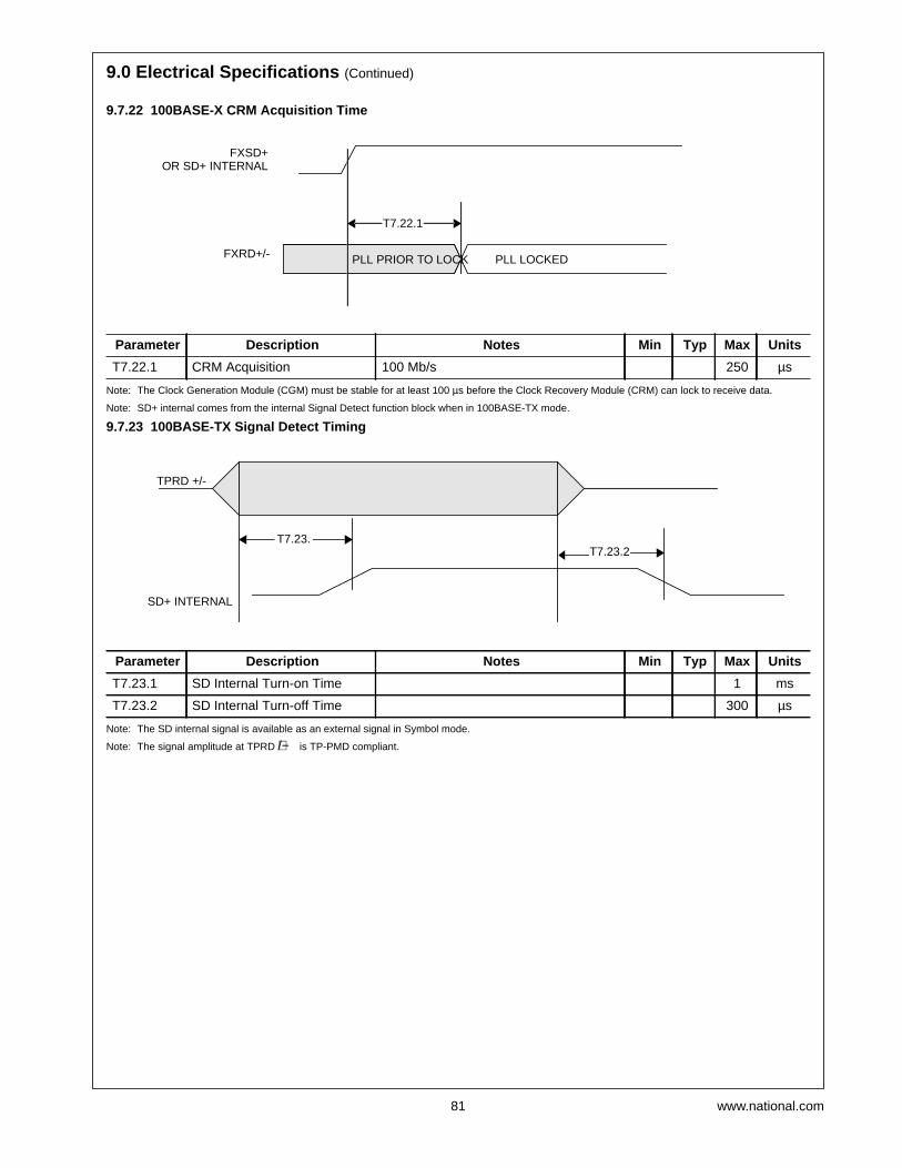
9.0 Electrical Specifications (Continued)
81 www.national.com
9.7.22 100BASE-X CRM Acquisition Time
Note: The Clock Generation Module (CGM) must be stable for at least 100 µs before the Clock Recovery Module (CRM) can lock to receive data.
Note: SD+ internal comes from the internal Signal Detect function block when in 100BASE-TX mode.
9.7.23 100BASE-TX Signal Detect Timing
Note: The SD internal signal is available as an external signal in Symbol mode.
Note: The signal amplitude at TPRD +/− is TP-PMD compliant.
Parameter Description Notes Min Typ Max Units
T7.22.1 CRM Acquisition 100 Mb/s 250 µs
Parameter Description Notes Min Typ Max Units
T7.23.1 SD Internal Turn-on Time 1 ms
T7.23.2 SD Internal Turn-off Time 300 µs
FXSD+
FXRD+/- PLL LOCKEDPLL PRIOR TO LOCK
T7.22.1
OR SD+ INTERNAL
T7.23.
SD+ INTERNAL
T7.23.2
TPRD +/-

9.0 Electrical Specifications (Continued)
82 www.national.com
9.8 Reset Timing
Note: Software Reset should be initiated no sooner then 500 µs after power-up or the deassertion of hardware reset.
Note: It is important to choose pull-up and/or pull-down resistors for each of the hardware configuration pins that provide fast RC time constants in order tolatch-in the proper value prior to the pin transitioning to an output driver.
Note: The timing for Hardware Reset Option 2 is equal to parameter T1 plus parameter T2 (501 µs total).
Parameter Description Notes Min Typ Max Units
T8.23.1 Internal Reset Time 500 µs
T8.23.2 Hardware RESET Pulse Width 1 µs
T8.23.3 Post Reset Stabilization timeprior to MDC preamble for reg-ister accesses
MDIO is pulled high for 32 bit serial man-agement initialization
500 µs
T8.23.4 Hardware Configuration Latch-in Time from the Deassertion ofReset (either soft or hard)
Hardware Configuration Pins are de-scribed in the Pin Description section
800 ns
T8.23.5 Hardware Configuration pinstransition to output drivers
It is important to choose pull-up and/orpull-down resistors for each of the hard-ware configuration pins that provide fastRC time constants in order to latch-in theproper value prior to the pin transitioningto an output driver
800 ns
VCC
HARDWARERESET (OPTION #1)
MDC
32 CLOCKS
LATCH-IN OF HARDWARECONFIGURATION PINS
DUAL FUNCTION PINSBECOME ENABLED AS OUTPUTS
INPUT OUTPUT
HARDWARERESET (OPTION #2)
T8.23.5
T8.23.
T8.23.T8.23.T8.23.
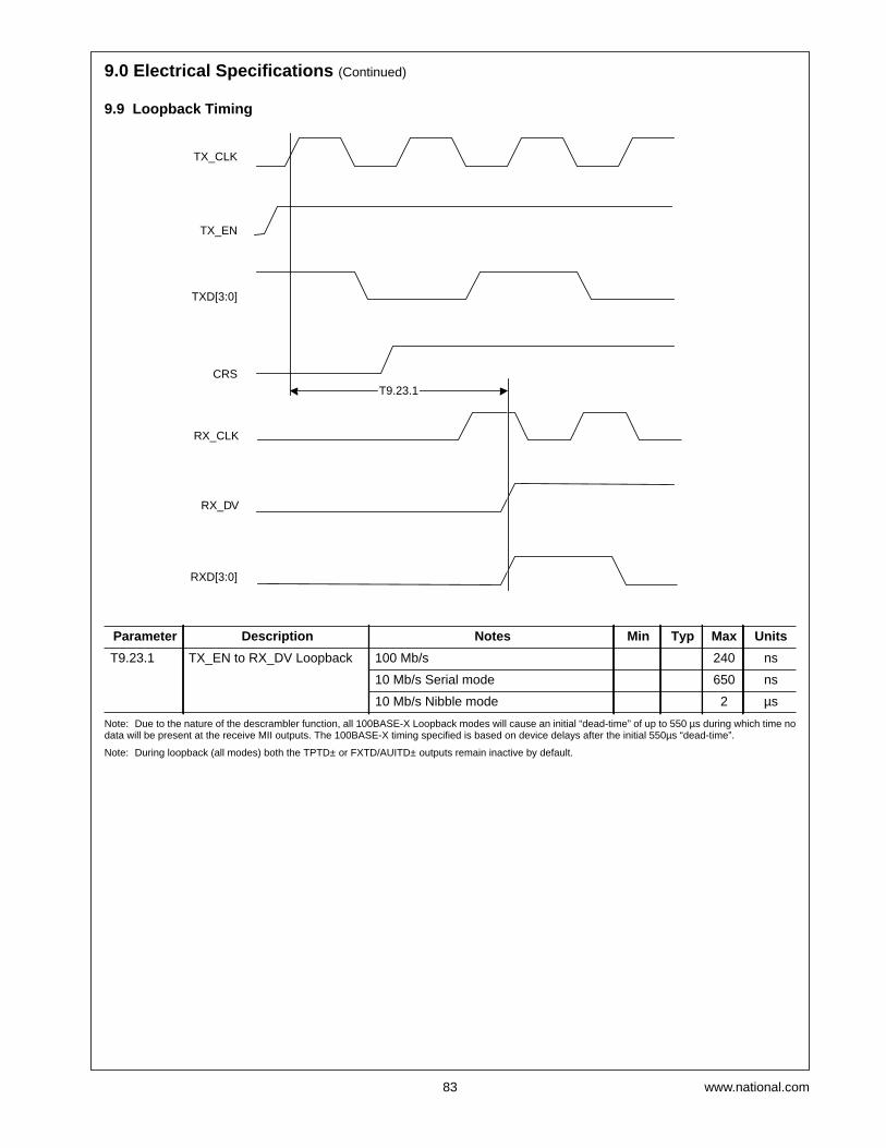
9.0 Electrical Specifications (Continued)
83 www.national.com
9.9 Loopback Timing
Note: Due to the nature of the descrambler function, all 100BASE-X Loopback modes will cause an initial “dead-time” of up to 550 µs during which time nodata will be present at the receive MII outputs. The 100BASE-X timing specified is based on device delays after the initial 550µs “dead-time”.
Note: During loopback (all modes) both the TPTD± or FXTD/AUITD± outputs remain inactive by default.
Parameter Description Notes Min Typ Max Units
T9.23.1 TX_EN to RX_DV Loopback 100 Mb/s 240 ns
10 Mb/s Serial mode 650 ns
10 Mb/s Nibble mode 2 µs
TX_CLK
TX_EN
TXD[3:0]
CRS
RX_CLK
RXD[3:0]
RX_DV
T9.23.1

9.0 Electrical Specifications (Continued)
84 www.national.com
9.10 Isolation Timing
Parameter Description Notes Min Typ Max Units
T10.23.1 From software clear of bit 10 inthe BMCR register to the transi-tion from Isolate to Normal Mode
100 µs
T10.23.2 From Deassertion of S/W or H/WReset to transition from Isolate toNormal mode
500 µs
CLEAR BIT 10 OF BMCR(RETURN TO NORMAL OPERATIONFROM ISOLATE MODE)
H/W OR S/W RESET(WITH PHYAD ≠ 00000)
MODEISOLATE NORMAL
T10.23.2
T10.23.1
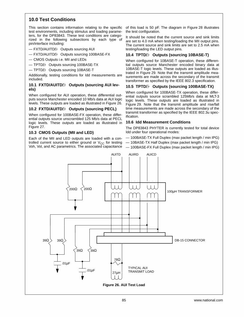
85 www.national.com
10.0 Test Conditions
This section contains information relating to the specifictest environments, including stimulus and loading parame-ters, for the DP83843. These test conditions are catego-rized in the following subsections by each type ofpin/interface including:— FXTD/AUITD+/− Outputs sourcing AUI— FXTD/AUITD+/− Outputs sourcing 100BASE-FX— CMOS Outputs i.e. MII and LEDs— TPTD+/− Outputs sourcing 100BASE-TX— TPTD+/− Outputs sourcing 10BASE-TAdditionally, testing conditions for Idd measurements areincluded.10.1 FXTD/AUITD+/− Outputs (sourcing AUI lev-els)When configured for AUI operation, these differential out-puts source Manchester encoded 10 Mb/s data at AUI logiclevels. These outputs are loaded as illustrated in Figure 26.10.2 FXTD/AUITD+/− Outputs (sourcing PECL)When configured for 100BASE-FX operation, these differ-ential outputs source unscrambled 125 Mb/s data at PECLlogic levels. These outputs are loaded as illustrated inFigure 27.10.3 CMOS Outputs (MII and LED)Each of the MII and LED outputs are loaded with a con-trolled current source to either ground or VCC for testingVoh, Vol, and AC parametrics. The associated capacitance
of this load is 50 pF. The diagram in Figure 28 illustratesthe test configuration.It should be noted that the current source and sink limitsare set to 4.0 mA when testing/loading the MII output pins.The current source and sink limits are set to 2.5 mA whentesting/loading the LED output pins.10.4 TPTD+/− Outputs (sourcing 10BASE-T)When configured for 10BASE-T operation, these differen-tial outputs source Manchester encoded binary data at10BASE-T logic levels. These outputs are loaded as illus-trated in Figure 29. Note that the transmit amplitude mea-surements are made across the secondary of the transmittransformer as specified by the IEEE 802.3 specification.10.5 TPTD+/− Outputs (sourcing 100BASE-TX)When configured for 100BASE-TX operation, these differ-ential outputs source scrambled 125Mb/s data at MLT-3logic levels. These outputs are loaded as illustrated inFigure 29. Note that the transmit amplitude and rise/falltime measurements are made across the secondary of thetransmit transformer as specified by the IEEE 802.3u spec-ification.10.6 Idd Measurement ConditionsThe DP83843 PHYTER is currently tested for total deviceIdd under four operational modes:— 100BASE-TX Full Duplex (max packet length / min IPG)— 10BASE-TX Half Duplex (max packet length / min IPG)— 100BASE-FX Full Duplex (max packet length / min IPG)
Figure 26. AUI Test Load
AUITD AUIRD AUICD
39Ω 39Ω
39Ω 39Ω
.01µF
.01µF
78Ω
27µH
200Ω 200Ω
TYPICAL AUITRANSMIT LOAD
100µH TRANSFORMER
DB-15 CONNECTOR
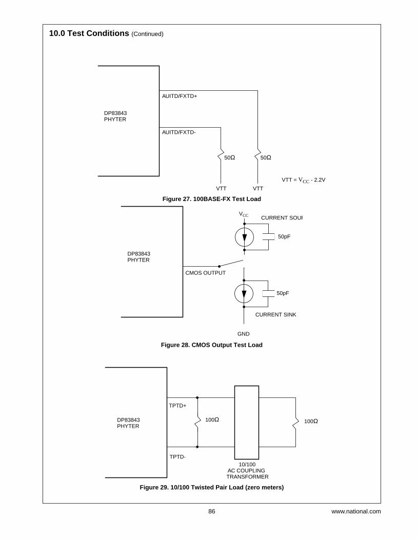
10.0 Test Conditions (Continued)
86 www.national.com
Figure 27. 100BASE-FX Test Load
Figure 28. CMOS Output Test Load
Figure 29. 10/100 Twisted Pair Load (zero meters)
DP83843PHYTER
VTT VTTVTT = VCC - 2.2V
50Ω 50Ω
AUITD/FXTD+
AUITD/FXTD-
DP83843PHYTER
GND
CMOS OUTPUT
VCC
50pF
50pF
CURRENT SINK
CURRENT SOUR
100Ω100Ω
10/100AC COUPLINGTRANSFORMER
DP83843PHYTER
TPTD-
TPTD+

MECHANICAL DATA
NNC0080A
www.ti.com

IMPORTANT NOTICETexas Instruments Incorporated and its subsidiaries (TI) reserve the right to make corrections, enhancements, improvements and otherchanges to its semiconductor products and services per JESD46, latest issue, and to discontinue any product or service per JESD48, latestissue. Buyers should obtain the latest relevant information before placing orders and should verify that such information is current andcomplete. All semiconductor products (also referred to herein as “components”) are sold subject to TI’s terms and conditions of salesupplied at the time of order acknowledgment.TI warrants performance of its components to the specifications applicable at the time of sale, in accordance with the warranty in TI’s termsand conditions of sale of semiconductor products. Testing and other quality control techniques are used to the extent TI deems necessaryto support this warranty. Except where mandated by applicable law, testing of all parameters of each component is not necessarilyperformed.TI assumes no liability for applications assistance or the design of Buyers’ products. Buyers are responsible for their products andapplications using TI components. To minimize the risks associated with Buyers’ products and applications, Buyers should provideadequate design and operating safeguards.TI does not warrant or represent that any license, either express or implied, is granted under any patent right, copyright, mask work right, orother intellectual property right relating to any combination, machine, or process in which TI components or services are used. Informationpublished by TI regarding third-party products or services does not constitute a license to use such products or services or a warranty orendorsement thereof. Use of such information may require a license from a third party under the patents or other intellectual property of thethird party, or a license from TI under the patents or other intellectual property of TI.Reproduction of significant portions of TI information in TI data books or data sheets is permissible only if reproduction is without alterationand is accompanied by all associated warranties, conditions, limitations, and notices. TI is not responsible or liable for such altereddocumentation. Information of third parties may be subject to additional restrictions.Resale of TI components or services with statements different from or beyond the parameters stated by TI for that component or servicevoids all express and any implied warranties for the associated TI component or service and is an unfair and deceptive business practice.TI is not responsible or liable for any such statements.Buyer acknowledges and agrees that it is solely responsible for compliance with all legal, regulatory and safety-related requirementsconcerning its products, and any use of TI components in its applications, notwithstanding any applications-related information or supportthat may be provided by TI. Buyer represents and agrees that it has all the necessary expertise to create and implement safeguards whichanticipate dangerous consequences of failures, monitor failures and their consequences, lessen the likelihood of failures that might causeharm and take appropriate remedial actions. Buyer will fully indemnify TI and its representatives against any damages arising out of the useof any TI components in safety-critical applications.In some cases, TI components may be promoted specifically to facilitate safety-related applications. With such components, TI’s goal is tohelp enable customers to design and create their own end-product solutions that meet applicable functional safety standards andrequirements. Nonetheless, such components are subject to these terms.No TI components are authorized for use in FDA Class III (or similar life-critical medical equipment) unless authorized officers of the partieshave executed a special agreement specifically governing such use.Only those TI components which TI has specifically designated as military grade or “enhanced plastic” are designed and intended for use inmilitary/aerospace applications or environments. Buyer acknowledges and agrees that any military or aerospace use of TI componentswhich have not been so designated is solely at the Buyer's risk, and that Buyer is solely responsible for compliance with all legal andregulatory requirements in connection with such use.TI has specifically designated certain components as meeting ISO/TS16949 requirements, mainly for automotive use. In any case of use ofnon-designated products, TI will not be responsible for any failure to meet ISO/TS16949.Products ApplicationsAudio www.ti.com/audio Automotive and Transportation www.ti.com/automotiveAmplifiers amplifier.ti.com Communications and Telecom www.ti.com/communicationsData Converters dataconverter.ti.com Computers and Peripherals www.ti.com/computersDLP® Products www.dlp.com Consumer Electronics www.ti.com/consumer-appsDSP dsp.ti.com Energy and Lighting www.ti.com/energyClocks and Timers www.ti.com/clocks Industrial www.ti.com/industrialInterface interface.ti.com Medical www.ti.com/medicalLogic logic.ti.com Security www.ti.com/securityPower Mgmt power.ti.com Space, Avionics and Defense www.ti.com/space-avionics-defenseMicrocontrollers microcontroller.ti.com Video and Imaging www.ti.com/videoRFID www.ti-rfid.comOMAP Applications Processors www.ti.com/omap TI E2E Community e2e.ti.comWireless Connectivity www.ti.com/wirelessconnectivity
Mailing Address: Texas Instruments, Post Office Box 655303, Dallas, Texas 75265Copyright © 2014, Texas Instruments Incorporated