Doing DSP Workshop Laboratory - · PDF fileDoing DSP WorkshopDRAFT Summer 2009 1 Introduction...
40
DRAFT Doing DSP Workshop Summer 2009 Lab Exercise 1 Contents 1 Introduction 3 2 Background 4 2.1 Spartan-3 Starter Board I/O devices .................... 4 2.1.1 LEDs ................................... 4 2.1.2 Slide switches ............................. 4 2.1.3 Seven-segment digit display ..................... 4 2.1.4 Push buttons .............................. 4 2.2 Addition ..................................... 4 2.2.1 Doing addition in VHDL ....................... 4 2.2.2 The one-bit full adder ........................ 5 2.2.3 Bit-parallel add/substract ...................... 5 2.2.4 Bit-serial adder ............................. 6 2.2.5 Bit-serial add/subtract unit ..................... 7 3 Prelab 7 3.1 ISE WebPACK Implementation Basics ................... 7 3.2 VHDL programming basics .......................... 8 3.3 Spartan-3 Starter Board Basics ....................... 8 4 Exercise 9 4.1 LEDs and slide switches ........................... 9 4.2 Blink the LEDs ................................. 11 4.3 Seven-segment LED displays ......................... 11 4.4 Seven-segment LED displays module ................... 11 4.4.1 Seven-Segment Display Module (SSD02.vhd) ........... 12 4.4.2 Using the Seven-Segment Display Module ............ 12 4.5 Processes and sequential statements ................... 14 4.6 Push buttons and debouncing ........................ 14 4.7 The VGA display ................................ 15 4.8 A push button timer with display ..................... 15 4.9 Serial and parallel adders .......................... 17 4.9.1 Full adder ................................ 17 4.9.2 VHDL’s adder .............................. 17 4.9.3 Four bit parallel adder ........................ 17 4.9.4 Four bit serial adder ......................... 17 A sw_led.vhd 19 Lab Exercise 1 1 May 12, 2009
-
Upload
vuongnguyet -
Category
Documents
-
view
214 -
download
1
Transcript of Doing DSP Workshop Laboratory - · PDF fileDoing DSP WorkshopDRAFT Summer 2009 1 Introduction...

DR
AFT
Doing DSP Workshop Summer 2009
Lab Exercise 1
Contents
1 Introduction 3
2 Background 4
2.1 Spartan3 Starter Board I/O devices . . . . . . . . . . . . . . . . . . . . 4
2.1.1 LEDs . . . . . . . . . . . . . . . . . . . . . . . . . . . . . . . . . . . 4
2.1.2 Slide switches . . . . . . . . . . . . . . . . . . . . . . . . . . . . . 4
2.1.3 Sevensegment digit display . . . . . . . . . . . . . . . . . . . . . 4
2.1.4 Push buttons . . . . . . . . . . . . . . . . . . . . . . . . . . . . . . 4
2.2 Addition . . . . . . . . . . . . . . . . . . . . . . . . . . . . . . . . . . . . . 4
2.2.1 Doing addition in VHDL . . . . . . . . . . . . . . . . . . . . . . . 4
2.2.2 The onebit full adder . . . . . . . . . . . . . . . . . . . . . . . . 5
2.2.3 Bitparallel add/substract . . . . . . . . . . . . . . . . . . . . . . 5
2.2.4 Bitserial adder . . . . . . . . . . . . . . . . . . . . . . . . . . . . . 6
2.2.5 Bitserial add/subtract unit . . . . . . . . . . . . . . . . . . . . . 7
3 Prelab 7
3.1 ISE WebPACK Implementation Basics . . . . . . . . . . . . . . . . . . . 7
3.2 VHDL programming basics . . . . . . . . . . . . . . . . . . . . . . . . . . 8
3.3 Spartan3 Starter Board Basics . . . . . . . . . . . . . . . . . . . . . . . 8
4 Exercise 9
4.1 LEDs and slide switches . . . . . . . . . . . . . . . . . . . . . . . . . . . 9
4.2 Blink the LEDs . . . . . . . . . . . . . . . . . . . . . . . . . . . . . . . . . 11
4.3 Sevensegment LED displays . . . . . . . . . . . . . . . . . . . . . . . . . 11
4.4 Sevensegment LED displays module . . . . . . . . . . . . . . . . . . . 11
4.4.1 SevenSegment Display Module (SSD02.vhd) . . . . . . . . . . . 12
4.4.2 Using the SevenSegment Display Module . . . . . . . . . . . . 12
4.5 Processes and sequential statements . . . . . . . . . . . . . . . . . . . 14
4.6 Push buttons and debouncing . . . . . . . . . . . . . . . . . . . . . . . . 14
4.7 The VGA display . . . . . . . . . . . . . . . . . . . . . . . . . . . . . . . . 15
4.8 A push button timer with display . . . . . . . . . . . . . . . . . . . . . 15
4.9 Serial and parallel adders . . . . . . . . . . . . . . . . . . . . . . . . . . 17
4.9.1 Full adder . . . . . . . . . . . . . . . . . . . . . . . . . . . . . . . . 17
4.9.2 VHDL’s adder . . . . . . . . . . . . . . . . . . . . . . . . . . . . . . 17
4.9.3 Four bit parallel adder . . . . . . . . . . . . . . . . . . . . . . . . 17
4.9.4 Four bit serial adder . . . . . . . . . . . . . . . . . . . . . . . . . 17
A sw_led.vhd 19
Lab Exercise 1 1 May 12, 2009

DR
AFT
Doing DSP Workshop Summer 2009
B sw_led.ucf 19
C SSD02.vhd 20
D SSD_top.vhd 23
E Spartan3SB.ucf 24
F pb_debounce.vhd 28
G pb_db_top.vhd 30
H VGA_top.vhd 31
I DCM_config.vhd 34
J timer01.vhd 37
K Onebit full adder entity VHDL 39
Lab Exercise 1 2 May 12, 2009

DR
AFT
Doing DSP Workshop Summer 2009
1 Introduction
In this lab exercise, we start to work with the Spartan3 FPGA starter board.
This includes the use of the software tool Xilinx ISE WebPACK and the basic
operation of the Spartan3 starter board. The programming language we use in
this workshop for FPGA is VHDL. Unlike the general DSP processor (e.g. C5510
DSP), the Spartan3 FPGA does not have prebuilt structure in it and its logic
is fully programmable. The starter board has a lot of useful peripherals and
user interface components. One of the objectives of this exercise is to get you
familiar with the starter board components and their functionalities. Basic VHDL
programming is also one of the skills we would like to equip you with in this lab
exercise.
Suggested reading
The documents and books listed here can be found in the workshop CD or in the
library.
• FPGA Prototyping by VHDL Examples: Xilinx Spartan3 Version, P. P. Chu,
Wiley 2008.
Digilent Spartan3 Starter Board:
• Spartan3 Starter Board User Guide
You really, really, really want to read the S3SB User’s Guide before doing this
exercise!
Xilinx ISE WebPACK:
• Xilinx ISE 10.1 Design Suite Software Manuals and Help
http://toolbox.xilinx.com/docsan/xilinx10/books/manuals.pdf
• ISE 10.1 Quick Start Tutorial
http://toolbox.xilinx.com/docsan/xilinx10/books/docs/qst/qst.pdf
VHDL Programming:
• Circuit Design with VHDL, V. A. Pedroni, MIT Press 2004.
• Advanced Digital Logic Design Using VHDL, State Machines, and Synthesis
for FPGAs, S. Lee, Thomson 2006.
• VHDL: A Starter’s Guide 2nd Ed., S. Yalamanchili, Pearson Prentice Hall
2005.
• The VHDL Reference: A Practical Guide to ComputerAided Integrated Cir
cuit Design, U. Heinkel et al., Wiley 2000.
• Other resources listed in the workshop website.
Lab Exercise 1 3 May 12, 2009

DR
AFT
Doing DSP Workshop Summer 2009
2 Background
We start by learning how to use the input and display devices and proceed to
using them in support roles when developing and testing logic for doing simple
arithmetic operations.
2.1 Spartan3 Starter Board I/O devices
These are extremely well documented in the Spartan3 Starter Board User Guide.
We won’t attempt to repeat that documentation here.
2.1.1 LEDs
There are eight.
2.1.2 Slide switches
There are eight. We will often add four additional slide switches using a PMod
unit.
2.1.3 Sevensegment digit display
There are four sevensegment digit displays.
2.1.4 Push buttons
There four push buttons. Because the contacts are not perfect there can be noise
on the break and make actions. Use of debouncers allow reliable operation.
2.2 Addition
A very fundamental arithmetic operation. Key to subtraction and multiplication.
Also important in dividing where one needs to do a lot of subtract and test
operations.
2.2.1 Doing addition in VHDL
It’s real easy. Use the +. To subtract, use the . The VHDL compiler (I believe)
implements/synthesizes a ripple carry adder or subtractor to do the calculation.
When to use +/ and when to implement one’s own adder/subtractor? Good
question. Probably a reasonable rule is whenever access is need to either the
carry in or carry out or when implementing an overflow indicator or maybe when
Lab Exercise 1 4 May 12, 2009

DR
AFT
Doing DSP Workshop Summer 2009
saturating. For a given situation try both ways and see how things work out. As
experience is gained choices sometimes will look more clear.
2.2.2 The onebit full adder
The full adder is the key element when implementing arithmetic operations. An
nbit adder is easily implemented by cascading n adders, carry out of one stage
feeding the following stage’s carry in. This is termed a ripple carry adder. A
ripple carry adder is what VHDL likely implements whenever you use +.
Ä~ ëÅáå
Å~êêó
ëìã
Åçìí
Figure 1: Single bit full adder block diagram.
Block diagram is contained in Figure 1.
Subtraction is most easily done by simply negating the value to be subtracted.
Invert the bits and put a one into the right most carry in to cause the addition of
1.
Multiplication is simply a method of doing repeated additions. For example
multiplying a value by 128 can be done adding that value into an accumulator
128 times.
We focus on binary multiplication but the methodology we use is the same as
we learned in grade school. Basically what we learned can be considered a fast
algorithm.
There clever tricks and reordering of operations (additions) that we can use
to simplify or speed things up. We will focus on bit serial methods because
of their minimal logic needs. Pretty much a classical logic amount vs time to
completion tradeoff.
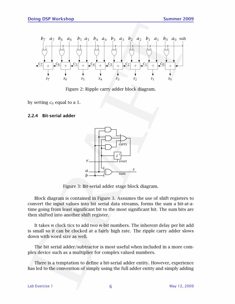
2.2.3 Bitparallel add/substract
Block diagram is contained in Figure 2. Subtraction of b from a is accomplished
by inverting the bits of b using exclusiveor gates and adding one to the result
Lab Exercise 1 5 May 12, 2009
DR
AFT
Doing DSP Workshop Summer 2009
ÅT
ÄN~T
ëM
ÅS ÅR
~R ~O ~N ~M~P~Q~S ÄOÄQ ÄP ÄMÄRÄT ÄS
ÅQ ÅP ÅO ÅN ÅM
ëNëOëPëQëRëSëT
ëìÄ
Figure 2: Ripple carry adder block diagram.
by setting c0 equal to a 1.
2.2.4 Bitserial adder
ò��
Ä~ ë
êÉëÉíê
Å~êêó
ëìã
Figure 3: Bitserial adder stage block diagram.
Block diagram is contained in Figure 3. Assumes the use of shift registers to
convert the input values into bit serial data streams, forms the sum a bitata
time going from least significant bit to the most significant bit. The sum bits are
then shifted into another shift register.
It takes n clock tics to add two nbit numbers. The inherent delay per bit add
is small so it can be clocked at a fairly high rate. The ripple carry adder slows
down with word size as well.
The bit serial adder/subtractor is most useful when included in a more com
plex device such as a multiplier for complex valued numbers.
There is a temptation to define a bitserial adder entity. However, experience
has led to the convention of simply using the full adder entity and simply adding
Lab Exercise 1 6 May 12, 2009

DR
AFT
Doing DSP Workshop Summer 2009
the delay at the next level. Six of one or half a dozen of the other. I might still
change my mind, again.
2.2.5 Bitserial add/subtract unit
~
Ä
ëÜáÑí=êÉÖáëíÉêëÅçìíÅáå
a
NJÄáí=~ÇÇÉê
ëÜáÑí=êÉÖáëíÉê
äëÄãëÄ äëÄãëÄ
áåáíá~äáòÉíç=M
ëìÄ
~±Ä
Figure 4: Bitserial adder/subtract unit block diagram.
Block diagram is contained in Figure 4. In lecture referred to as Alternate
configuration 1. The delay stage connected between cin and cout is initialized to
zero regardless whether adding or subtracting. The cost of this “feature” is one
exclusiveor gate.
3 Prelab
Here is a list of questions to get your familiar with the concepts covered in this
lab exercise and prepare you to do the lab exercise. Read the questions and try
to figure out the answers.
3.1 ISE WebPACK Implementation Basics
Answering the following question about using the ISE WebPACK. You might want
to use the “Help” function in the software to look for the answers.
1. What is the basic FPGA design flow? (7 steps in ISE Help).
2. What is a user constraints file (UCF)?
3. What are the methods that can be used for editing/entering constraints in
a UCF file?
Lab Exercise 1 7 May 12, 2009

DR
AFT
Doing DSP Workshop Summer 2009
4. What are the implementation design process steps for FPGA in ISE? (ISE
Help)
5. What is iMPACT in the ISE WebPACK and what does it do?
3.2 VHDL programming basics
Answer the following questions by reading the VHDL references or googling the
Internet.
1. What does VHDL stand for?
2. What is an “entity” in VHDL?
3. What is an “architecture” in VHDL? What are the two types of descriptions
used to describe the architecture?
4. What is a “process” in VHDL?
5. What is the “sensitivity list” of a process?
3.3 Spartan3 Starter Board Basics
Read the Spartan3 Starter Kit Board User Guide and then answer the following
questions.
1. Is there a clock source on the Spartan3 FPGA board? If so, what is the
clock rate?
2. What is the total size of onchip block RAM of the Spartan3 FPGA?
3. What is the total size of onboard SRAM of the starter board?
4. How many 40pin expansion connectors are on the starter board?
5. What voltage can be outputted from the 40pin connectors?
6. What are the pins connected to the sevensegment LEDs, LEDs, slide switches,
and push buttons on the board?
7. Where can you find information about the pins connected to the B1 expan
sion connectors on the board? (documentation and page number)
8. There is only one set of pins connecting to the segments for the four seven
segment LED displays. How can we individually control four digits using
only one set of pins connected to segments of all four digits?
Lab Exercise 1 8 May 12, 2009

DR
AFT
Doing DSP Workshop Summer 2009
4 Exercise
4.1 LEDs and slide switches
In this part of the exercise, you will use ISE WebPACK to build a simple project to
control the on/off of the LEDs using the slide switches. Do the following steps:
• Start a new project named sw_led in ISE using the new project wizard
(File→New Project).
• Create a new VHDL module source file named sw_led and add it to the
project.
• Specify an input bus sw of 8 bits (MSB: 7, LSB: 0) for the slide switches and
a output bus led of 8 bits for the LEDs. After these steps, you should see
the code in the project navigator window as shown in Figure 5.
• In the project navigator, open the source file you just created. In the source
file, declare two signals called “input” and “output” as 8bit standard logic
vectors.
• Write the code to assign the slide switch value to the signal “input”, assign
the signal “input” to the signal “output”, and assign the signal “output” to
the LED output. See section A for the VHDL code.
• Edit the user constraints file for the I/O pins of the project (use the text
editor). Map SWi to LDi for i = 0, 1,· · · , 7. See section B for the ucf file
format. Fill in ?? with the corresponding pins numbers in your Prelab. Save
the file with .ucf extension and add it to the project.
• Synthesize the code, implement the design, and generate the programming
file.
• Load the programming file to the FPGA using iMPACT.
After you successfully load the program to the chip, you should be able to
control the LEDs using the slide switches.
Can you further simplify the code listed in section A to achieve the same
task? How will you modify the code?
Lab Exercise 1 9 May 12, 2009

DR
AFT
Doing DSP Workshop Summer 2009
Figure 5: Unedited VHDL code
Lab Exercise 1 10 May 12, 2009

DR
AFT
Doing DSP Workshop Summer 2009
4.2 Blink the LEDs
In this part of the exercise, create a simple project to blink the one (or more) of
the LEDs. Say we want to blink the LED at 1 Hz (LED on for 0.5 second and off
for 0.5 second). In order to control the timing, we need a clock source. There is
a 50 MHz master clack on the Spartan3 starter board. There are various ways
to implement this task. One possible solutions is to generate a 1 Hz clock signal
with 50% duty cycle and use this clock to drive the LED.
The question now is how to generate a 1 Hz clock from a 50 MHz clock? It can
simply be done by using a counter to count the 50 MHz clock and alternate the 1
Hz clock signal (0 to 1 or 1 to 0). The counter is increased by 1 at every 50 MHz
clock tick. The 1 Hz clock signal is altered every 25000000 50 MHz clock ticks.
In order to check the 50 MHz clock and the counter, the if statement in VHDL
can be used. However, in VHDL, if statement can only be used within a process.
To understand this , refer to the VHDL references. Here is an example of using
the 50 MHz clock (mclk) and a counter (ctr) to generate the 1 Hz clock (clk). Note
that all the signals should be declared/defined in entity or in architecture.
process(mclk)
begin
if rising_edge(mclk) then
ctr <= ctr + 1;
if ctr = 24999999 then
clk <= not clk;
ctr <= 0;
end if;
end if;
end process;
4.3 Sevensegment LED displays
In this part of the exercise, create a simple project using the slide switches to
control the sevensegment LED displays. There is an example provided in the
Meeting 2 discussion note. However, that example is build on the Basys board. In
order to make it work on the Spartan3 board, you have to create a corresponding
UCF file. Try to understand how sevensegment LED display and the example
code work and implement it in the lab.
4.4 Sevensegment LED displays module
In this part of the exercise, you will learn how to use the sevensegment LED
display VHDL module (SSD02) used in the EECS 452 lab. This is a module that
makes it easy to generate hex number patterns using the sevensegment LED
displays. The input to the module are 4 hex numbers and the output of the
module are signals (with corresponding patterns) to drive the sevensegment
Lab Exercise 1 11 May 12, 2009

DR
AFT
Doing DSP Workshop Summer 2009
LED displays. You will also learn how to integrate a VHDL module into your
project in a layered coding structure (module(entity) within a module(entity)).
4.4.1 SevenSegment Display Module (SSD02.vhd)
This module is designed for using the four sevensegment displays. The signal
sel is a fourbit vector used to activate the 4 displays. sel(i) controls ssdi for
i = 0,1,2,3. “1” turns the display on the “0” turns it off. The dp array is used to
light the four radix points (not shown here)(1→on, 0→off). When sel=“0000”, the
4 sevensegment displays look like the following
ssd3 ssd2 ssd1 ssd0
To use ssd2, ssd1, and ssd0 to display 4, 5, 2, respectively, we set sel=“0111”,
ssd3=“xxxx”(any number), ssd2=“0100”, ssd1=“0101”, and ssd0=“0010”. The
sevensegment display will look like the following
ssd3 ssd2 ssd1 ssd0
Here is the list all the hex numbers that can be displayed using this module.
If you want to display something more, you need to modify it according to your
needs. See section C for the VHDL code.
4.4.2 Using the SevenSegment Display Module
• Create a new project in ISE.
• Create a new source file called “SSD_top” with the following I/O signals:
– mclk : input
– ssg : output bus (7 downto 0)
– an : inout bus (3 downto 0)
Lab Exercise 1 12 May 12, 2009

DR
AFT
Doing DSP Workshop Summer 2009
• Declare the following signals:
– ssd0 : 4bit standard logic vector
– ssd1 : 4bit standard logic vector
– ssd2 : 4bit standard logic vector
– ssd3 : 4bit standard logic vector
– dp : 4bit standard logic vector
– ssd_select : 4bit standard logic vector
• Add the following to the main code SSD_top
SSD02_unit : entity work.SSD02 sevensegment display module
port map (
ssd0 => ssd0(3 downto 0),
ssd1 => ssd1(3 downto 0),
ssd2 => ssd2(3 downto 0),
ssd3 => ssd3(3 downto 0),
ssd => ssg,
dp => dp,
sel => ssd_select,
an => an,
clk => mclk);
This is how to include a module (entity) within the current design. SSD02_unit
is a label, which is optional. entity work.SSD02 is to include the SSD02 en
tity from the work library. This is a special library that can be used without
specifying it in the VHDL source code. The compiler treats it as the current
working area (folder) in which all the design hierarchy entities reside. The
port map is similar to the port in the entity definition. It maps the signals
defined in the entity of the module being included to the signals in the cur
rent source. The symbol “=>” simply indicates the mapping (connection of
signals/nodes) instead of assignment.
• Add the source file SSD02.vhd to the project. At this point, you should
have the code as shown in section D.
• Add the user constraints file Spartan3SB.ucf as shown in section E to the
project. You might need to edit the ucf file (comment/uncomment) to
match the I/O signals defined in the entity.
• Complete the project by add codes to the source file to display “EECS” in
the four sevensegment displays.
ssd3 ssd2 ssd1 ssd0
Lab Exercise 1 13 May 12, 2009

DR
AFT
Doing DSP Workshop Summer 2009
• The current module only supports hex numbers. What if you want to dis
play other symbols/letters? You might consider modify this module or
create your own module.
4.5 Processes and sequential statements
A big difference between VHDL and other programming languages such as C or
Matlab is that in VHDL, all statements within an architecture operates concur
rently while in C or Matlab, all the statements are executed sequentially. Thus,
it is necessary for VHDL to be able to handle sequential behavior. A process,
as a whole, is treated concurrently as other statements within an architecture.
However, the statements within a process are executed one after another as in
conventional programming languages.
4.6 Push buttons and debouncing
The push button consists of a simple mechanical contact. Whenever you push
and release it to make the contacts close and open, inertia may cause the con
tacts to bounce. Therefore, we need to debounce the push button to eliminate
the inferior mechanical contacts and determination the state of the push button.
There are two types of push button switch: normally open (NO) and normally
closed (NC). You press the button and the contacts will open and close many
times before finally staying in position. This is known as contact bounce. De
pending on the switch construction, this mechanical contact bounce can last up
to 20 milliseconds. This isn’t a problem for lamps, doorbells and audio circuits,
but it will play havoc to a fast switching logic circuit or computer.
A VHDL module pb_debounce.vhd G in the lab support files is used for push
button debouncing. Take a look at the code and try to understand how it works.
This code can/will be used in the future lab exercises and projects.
In this part of the exercise you will build a project to test a push button
debounce module.The VHDL model pb_debounce.vhd can be found in section F.
• Create a new project and add the following source files.
Lab Exercise 1 14 May 12, 2009

DR
AFT
Doing DSP Workshop Summer 2009
– pb_db_top.vhd (see section G)
– pb_debounce.vhd
– Spartan3SB.ucf
• Modify the UCF file accordingly and build up the program.
• What are the functions of the switches (sw7 and sw(3 downto 0)), push
button 0, LED 0 and LED 7 in this exercise?
4.7 The VGA display
In this part of the exercise, we generate VGA signals and output to the LCD
display via the VGA connector on the spartan3 board. In the exercise you will
generate a 1024 x 768 pixels display with 70 Hz frame rate. The pixel clock is
75 MHz and is generated using the 50 MHz on board clock and the Xilinx digital
clock manager (DCM) module.
Use the files VGA_top.vhd, DCM_config.vhd, and Spartan3SB.ucf as shown in
section H, I, and E to build a project in ISE. Remember to comment or uncomment
the necessary/unnecessary I/O pins in the UCF file for this specific project. After
you build the project, connect the LCD monitor analog input cable to the VGA
output connector on the spartan3 board and switch the monitor to display the
analog input. You should see the following pattern shown on the screen.
4.8 A push button timer with display
In this part of the exercise, the push button, the debouncing module, the seven
segment LED display, processes are all integrated into one project performing
the function of a timer. The timer program will start to time when you press
push button 0 and display the timing using the sevensegment display in seconds
in hexadecimal number.
• Create a new project and add the following source files to the project.
Lab Exercise 1 15 May 12, 2009

DR
AFT
Doing DSP Workshop Summer 2009
– timer01.vhd (see section J)
– SSD02.vhd
– pb_debounce.vhd
– Spartan3SB.ucf
• You need to generate a 1 Hz clock using the on board 50 MHz clock. Theeasiest way is to use a counter. This part of the code is as the following
...when st_pb0_pushed =>if pb_db(0) = ’1’ then
next_pb_clear <= "0001";next_state <= st_idle;
elsenext_clk_counter <= clk_counter + ????; counter used to generate 1Hz clockif clk_counter = ???? then
next_clk_counter <= X"0000000";next_counter <= counter + ????;
end if;next_display <= next_counter;next_state <= st_pb0_pushed;
end if;...
What should the missing parts marked with ???? be to make this work?
• Find out what are the functions of push button 0 and push button 3 in the
project?
• Fill the blanks (marked with ????) to connect the debouncing and sevensegment display modules to the top file.
push_buttons : entity work.pb_debounce push button debouncer
port map (
pb_in => ????, input actual push buttons
pb_out => ????, debounced push button
pb_clear => ????, clears the button state
reset => ????,
clk => ????);
SSD02_unit : entity work.SSD02 sevensegment display
port map (
ssd0 => ????,
ssd1 => ????,
ssd2 => ????,
ssd3 => ????,
ssd => ????,
dp => ????,
sel => ????,
an => ????,
clk => ????);
• Modify the UCF file accordingly.
Lab Exercise 1 16 May 12, 2009

DR
AFT
Doing DSP Workshop Summer 2009
4.9 Serial and parallel adders
The PMod slide switches are read in as std_logic_vector(3 downto 0). A
zero is read when a switch is in the down position and one is read when a switch
is in the up position.
4.9.1 Full adder
In lecture a onebit full adder was used to illustrated basic binary addition. Using
the code in the lecture notes or your own variation make a working implementa
tion using the S3SB. It should work as desired.
4.9.2 VHDL’s adder
Mentally divide the eight slide switches into two 4 switch registers, the low four
switches and the high four. Generate a project that uses the VHDL + operator
to add the two fourbit values and display the sum using the right most seven
segment digits. Also display the sum in the low four leds.
4.9.3 Four bit parallel adder
As before but using the full adder entity make your own four bit adder entity.
The entity should have a carry in, two four bit inputs, a carry out and overflow
out.
Display as before with the following additions:
• LED7 should light if there has been an overflow, assuming two’s comple
ment 4bit values.
• LED4 should display the carry out of the most significant bit.
A modification is to assume the four bit values are two’s complement values
and display the absolute value of the sum in the seven segment digit. It would
nice to use the adjacent digit middle bar to display a minus sign but alas this is
not all that easy given the existing entities. The problem is more acute if we want
to sign a value displayed in all four digits. Maybe turn on all the radix points
when displaying a negative value?
4.9.4 Four bit serial adder
The bitserial adder structure was discussed in lecture. The implementation is
somewhat more complicated because of the need for shift register. Bitserial
addition is a sequential process and benefits greatly from using a state machine.
Lab Exercise 1 17 May 12, 2009

DR
AFT
Doing DSP Workshop Summer 2009
Create a four bit serial adder that does the same functions as were imple
mented for the four bit parallel adder.
Lab Exercise 1 18 May 12, 2009

DR
AFT
Doing DSP Workshop Summer 2009
A sw_led.vhd
Company: Engineer: Create Date: 23:55:47 01/10/2007 Design Name: Module Name: sw_led Behavioral Project Name: Target Devices: Tool versions: Description: Dependencies: Revision: Revision 0.01 File Created Additional Comments:library IEEE;use IEEE.STD_LOGIC_1164.ALL;use IEEE.STD_LOGIC_ARITH.ALL;use IEEE.STD_LOGIC_UNSIGNED.ALL;
Uncomment the following library declaration if instantiating any Xilinx primitives in this code.library UNISIM;use UNISIM.VComponents.all;
entity sw_led isPort ( sw : in STD_LOGIC_VECTOR (7 downto 0);
led : out STD_LOGIC_VECTOR (7 downto 0));end sw_led;
architecture Behavioral of sw_led is
signal input : std_logic_vector (7 downto 0);signal output : std_logic_vector (7 downto 0);
begin
input <= sw;output <= input;led <= output;
end Behavioral;
B sw_led.ucf
NET "sw<0>" LOC = "??";NET "sw<1>" LOC = "??";NET "sw<2>" LOC = "??";NET "sw<3>" LOC = "??";NET "sw<4>" LOC = "??";NET "sw<5>" LOC = "??";NET "sw<6>" LOC = "??";NET "sw<7>" LOC = "??";
Lab Exercise 1 19 May 12, 2009

DR
AFT
Doing DSP Workshop Summer 2009
NET "led<0>" LOC = "??";NET "led<1>" LOC = "??";NET "led<2>" LOC = "??";NET "led<3>" LOC = "??";NET "led<4>" LOC = "??";NET "led<5>" LOC = "??";NET "led<6>" LOC = "??";NET "led<7>" LOC = "??";
C SSD02.vhd
Company: UM EECS 452 Engineer: ChihWei Wang Create Date: 16:35:23 10/07/2006 Design Name: Module Name: 7seg_LED_display Behavioral Project Name: Target Devices: Tool versions: Description: Dependencies: Revision: Revision 0.01 File Created Additional Comments:library IEEE;use IEEE.STD_LOGIC_1164.ALL;use IEEE.STD_LOGIC_ARITH.ALL;use IEEE.STD_LOGIC_UNSIGNED.ALL;
Uncomment the following library declaration if instantiating any Xilinx primitives in this code.library UNISIM;use UNISIM.VComponents.all;
entity SSD02 isPort ( ssd0 : in STD_LOGIC_VECTOR (3 downto 0);
ssd1 : in STD_LOGIC_VECTOR (3 downto 0);ssd2 : in STD_LOGIC_VECTOR (3 downto 0);ssd3 : in STD_LOGIC_VECTOR (3 downto 0);ssd : out STD_LOGIC_VECTOR (7 downto 0);dp : in STD_LOGIC_VECTOR (3 downto 0);sel : in STD_LOGIC_VECTOR (3 downto 0);an : inout STD_LOGIC_VECTOR (3 downto 0);clk : in STD_LOGIC);
end SSD02;
architecture Behavioral of SSD02 is
constant num0 : STD_LOGIC_VECTOR(6 downto 0) := "0000001"; 0constant num1 : STD_LOGIC_VECTOR(6 downto 0) := "1001111"; 1constant num2 : STD_LOGIC_VECTOR(6 downto 0) := "0010010"; 2constant num3 : STD_LOGIC_VECTOR(6 downto 0) := "0000110"; 3constant num4 : STD_LOGIC_VECTOR(6 downto 0) := "1001100"; 4constant num5 : STD_LOGIC_VECTOR(6 downto 0) := "0100100"; 5constant num6 : STD_LOGIC_VECTOR(6 downto 0) := "0100000"; 6constant num7 : STD_LOGIC_VECTOR(6 downto 0) := "0001111"; 7
Lab Exercise 1 20 May 12, 2009

DR
AFT
Doing DSP Workshop Summer 2009
constant num8 : STD_LOGIC_VECTOR(6 downto 0) := "0000000"; 8constant num9 : STD_LOGIC_VECTOR(6 downto 0) := "0001100"; 9constant num10 : STD_LOGIC_VECTOR(6 downto 0) := "0001000"; Aconstant num11 : STD_LOGIC_VECTOR(6 downto 0) := "1100000"; Bconstant num12 : STD_LOGIC_VECTOR(6 downto 0) := "0110001"; Cconstant num13 : STD_LOGIC_VECTOR(6 downto 0) := "1000010"; Dconstant num14 : STD_LOGIC_VECTOR(6 downto 0) := "0110000"; Econstant num15 : STD_LOGIC_VECTOR(6 downto 0) := "0111000"; F
signal ssd_0 : std_logic_vector(7 downto 0);signal ssd_1 : std_logic_vector(7 downto 0);signal ssd_2 : std_logic_vector(7 downto 0);signal ssd_3 : std_logic_vector(7 downto 0);signal ctr: std_logic_vector(12 downto 0);
begin
SSD_select : process(sel)beginif sel(0) = ’0’ then
ssd_0(6 downto 0) <= "1111111";else
case ssd0 iswhen "0000" => ssd_0(6 downto 0) <= num0;when "0001" => ssd_0(6 downto 0) <= num1;when "0010" => ssd_0(6 downto 0) <= num2;when "0011" => ssd_0(6 downto 0) <= num3;when "0100" => ssd_0(6 downto 0) <= num4;when "0101" => ssd_0(6 downto 0) <= num5;when "0110" => ssd_0(6 downto 0) <= num6;when "0111" => ssd_0(6 downto 0) <= num7;when "1000" => ssd_0(6 downto 0) <= num8;when "1001" => ssd_0(6 downto 0) <= num9;when "1010" => ssd_0(6 downto 0) <= num10;when "1011" => ssd_0(6 downto 0) <= num11;when "1100" => ssd_0(6 downto 0) <= num12;when "1101" => ssd_0(6 downto 0) <= num13;when "1110" => ssd_0(6 downto 0) <= num14;when others => ssd_0(6 downto 0) <= num15;
end case;end if;if sel(1) = ’0’ then
ssd_1(6 downto 0) <= "1111111";else
case ssd1 iswhen "0000" => ssd_1(6 downto 0) <= num0;when "0001" => ssd_1(6 downto 0) <= num1;when "0010" => ssd_1(6 downto 0) <= num2;when "0011" => ssd_1(6 downto 0) <= num3;when "0100" => ssd_1(6 downto 0) <= num4;when "0101" => ssd_1(6 downto 0) <= num5;when "0110" => ssd_1(6 downto 0) <= num6;when "0111" => ssd_1(6 downto 0) <= num7;when "1000" => ssd_1(6 downto 0) <= num8;when "1001" => ssd_1(6 downto 0) <= num9;when "1010" => ssd_1(6 downto 0) <= num10;when "1011" => ssd_1(6 downto 0) <= num11;when "1100" => ssd_1(6 downto 0) <= num12;when "1101" => ssd_1(6 downto 0) <= num13;when "1110" => ssd_1(6 downto 0) <= num14;when others => ssd_1(6 downto 0) <= num15;
end case;end if;if sel(2) = ’0’ then
Lab Exercise 1 21 May 12, 2009

DR
AFT
Doing DSP Workshop Summer 2009
ssd_2(6 downto 0) <= "1111111";else
case ssd2 iswhen "0000" => ssd_2(6 downto 0) <= num0;when "0001" => ssd_2(6 downto 0) <= num1;when "0010" => ssd_2(6 downto 0) <= num2;when "0011" => ssd_2(6 downto 0) <= num3;when "0100" => ssd_2(6 downto 0) <= num4;when "0101" => ssd_2(6 downto 0) <= num5;when "0110" => ssd_2(6 downto 0) <= num6;when "0111" => ssd_2(6 downto 0) <= num7;when "1000" => ssd_2(6 downto 0) <= num8;when "1001" => ssd_2(6 downto 0) <= num9;when "1010" => ssd_2(6 downto 0) <= num10;when "1011" => ssd_2(6 downto 0) <= num11;when "1100" => ssd_2(6 downto 0) <= num12;when "1101" => ssd_2(6 downto 0) <= num13;when "1110" => ssd_2(6 downto 0) <= num14;when others => ssd_2(6 downto 0) <= num15;
end case;end if;if sel(3) = ’0’ then
ssd_3(6 downto 0) <= "1111111";else
case ssd3 iswhen "0000" => ssd_3(6 downto 0) <= num0;when "0001" => ssd_3(6 downto 0) <= num1;when "0010" => ssd_3(6 downto 0) <= num2;when "0011" => ssd_3(6 downto 0) <= num3;when "0100" => ssd_3(6 downto 0) <= num4;when "0101" => ssd_3(6 downto 0) <= num5;when "0110" => ssd_3(6 downto 0) <= num6;when "0111" => ssd_3(6 downto 0) <= num7;when "1000" => ssd_3(6 downto 0) <= num8;when "1001" => ssd_3(6 downto 0) <= num9;when "1010" => ssd_3(6 downto 0) <= num10;when "1011" => ssd_3(6 downto 0) <= num11;when "1100" => ssd_3(6 downto 0) <= num12;when "1101" => ssd_3(6 downto 0) <= num13;when "1110" => ssd_3(6 downto 0) <= num14;when others => ssd_3(6 downto 0) <= num15;
end case;end if;
end process SSD_select;
ssd_0(7) <= not dp(0);ssd_1(7) <= not dp(1);ssd_2(7) <= not dp(2);ssd_3(7) <= not dp(3);
SSD main unitprocess (clk)begin
if clk’event and clk = ’1’ thenif (ctr="0000000000000") then
if (an(3)=’0’) thenan(3) <= ’1’;ssd <= ssd_2; led2an(2) <= ’0’;
elsif (an(2)=’0’) thenan(2) <= ’1’;ssd <= ssd_1; led1an(1) <= ’0’;
elsif (an(1)=’0’) then
Lab Exercise 1 22 May 12, 2009

DR
AFT
Doing DSP Workshop Summer 2009
an(1) <= ’1’;ssd <= ssd_0; led0an(0) <= ’0’;
elsif (an(0)=’0’) thenan(0) <= ’1’;ssd <= ssd_3; led3an(3) <= ’0’;
end if;end if;ctr <= ctr+"0000000000001";if (ctr > "1000000000000") then
CTR <= "0000000000000";end if;
end if;end process;
end Behavioral;
D SSD_top.vhd
Company: Engineer: Create Date: 13:15:19 09/18/2008 Design Name: Module Name: SSD_top Behavioral Project Name: Target Devices: Tool versions: Description: Dependencies: Revision: Revision 0.01 File Created Additional Comments:library IEEE;use IEEE.STD_LOGIC_1164.ALL;use IEEE.STD_LOGIC_ARITH.ALL;use IEEE.STD_LOGIC_UNSIGNED.ALL;
Uncomment the following library declaration if instantiating any Xilinx primitives in this code.library UNISIM;use UNISIM.VComponents.all;
entity SSD_top isPort ( mclk : in STD_LOGIC;
ssg : out STD_LOGIC_VECTOR (7 downto 0);an : inout STD_LOGIC_VECTOR (3 downto 0));
end SSD_top;
architecture Behavioral of SSD_top is
signal ssd0: STD_LOGIC_VECTOR(3 downto 0);signal ssd1: STD_LOGIC_VECTOR(3 downto 0);signal ssd2: STD_LOGIC_VECTOR(3 downto 0);signal ssd3: STD_LOGIC_VECTOR(3 downto 0);
Lab Exercise 1 23 May 12, 2009

DR
AFT
Doing DSP Workshop Summer 2009
signal dp : STD_LOGIC_VECTOR(3 downto 0);signal ssd_select : STD_LOGIC_VECTOR(3 downto 0);
begin
SSD02_unit : entity work.SSD02 seven segment display moduleport map (
ssd0 => ssd0(3 downto 0),ssd1 => ssd1(3 downto 0),ssd2 => ssd2(3 downto 0),ssd3 => ssd3(3 downto 0),ssd => ssg,dp => dp,sel => ssd_select,an => an,clk => mclk);
end Behavioral;
E Spartan3SB.ucf
# Spartan3 User Constraints File: spartan3.ucf## 11Jan2007# 04Dec2007 .. fixed RAM A data bit 8, added McBSP 1 .. KM# 27Mar2008 .. added misc A2 pins .. KM#
# oscillator clock (in)#NET "mclk" PERIOD = 20 ns HIGH 40 %;NET "mclk" LOC = "T9" | IOSTANDARD = LVCMOS33;
# push buttons##NET "btn<0>" LOC = "M13" | IOSTANDARD = LVCMOS33;#NET "btn<1>" LOC = "M14" | IOSTANDARD = LVCMOS33;#NET "btn<2>" LOC = "L13" | IOSTANDARD = LVCMOS33;#NET "btn<3>" LOC = "L14" | IOSTANDARD = LVCMOS33;
# light emitting diodes##NET "led<0>" LOC = "K12" | IOSTANDARD = LVCMOS33;#NET "led<1>" LOC = "P14" | IOSTANDARD = LVCMOS33;#NET "led<2>" LOC = "L12" | IOSTANDARD = LVCMOS33;#NET "led<3>" LOC = "N14" | IOSTANDARD = LVCMOS33;#NET "led<4>" LOC = "P13" | IOSTANDARD = LVCMOS33;#NET "led<5>" LOC = "N12" | IOSTANDARD = LVCMOS33;#NET "led<6>" LOC = "P12" | IOSTANDARD = LVCMOS33;#NET "led<7>" LOC = "P11" | IOSTANDARD = LVCMOS33;
# seven segment digit anodes##NET "an<0>" LOC = "D14" | IOSTANDARD = LVCMOS33;#NET "an<1>" LOC = "G14" | IOSTANDARD = LVCMOS33;#NET "an<2>" LOC = "F14" | IOSTANDARD = LVCMOS33;#NET "an<3>" LOC = "E13" | IOSTANDARD = LVCMOS33;
# seven segment digit cathodes##NET "ssg<0>" LOC = "N16" | IOSTANDARD = LVCMOS33; # segment G
Lab Exercise 1 24 May 12, 2009

DR
AFT
Doing DSP Workshop Summer 2009
#NET "ssg<1>" LOC = "F13" | IOSTANDARD = LVCMOS33; # segment F#NET "ssg<2>" LOC = "R16" | IOSTANDARD = LVCMOS33; # segment E#NET "ssg<3>" LOC = "P15" | IOSTANDARD = LVCMOS33; # segment D#NET "ssg<4>" LOC = "N15" | IOSTANDARD = LVCMOS33; # segment C#NET "ssg<5>" LOC = "G13" | IOSTANDARD = LVCMOS33; # segment B#NET "ssg<6>" LOC = "E14" | IOSTANDARD = LVCMOS33; # segment A#NET "ssg<7>" LOC = "P16" | IOSTANDARD = LVCMOS33; # dp(decimal point)
# slide switches##NET "swt<0>" LOC = "F12" | IOSTANDARD = LVCMOS33;#NET "swt<1>" LOC = "G12" | IOSTANDARD = LVCMOS33;#NET "swt<2>" LOC = "H14" | IOSTANDARD = LVCMOS33;#NET "swt<3>" LOC = "H13" | IOSTANDARD = LVCMOS33;#NET "swt<4>" LOC = "J14" | IOSTANDARD = LVCMOS33;#NET "swt<5>" LOC = "J13" | IOSTANDARD = LVCMOS33;#NET "swt<6>" LOC = "K14" | IOSTANDARD = LVCMOS33;#NET "swt<7>" LOC = "K13" | IOSTANDARD = LVCMOS33;
# DB15 video connector##NET "blu" LOC = "R11" | IOSTANDARD = LVCMOS33;#NET "grn" LOC = "T12" | IOSTANDARD = LVCMOS33;#NET "red" LOC = "R12" | IOSTANDARD = LVCMOS33;#NET "hs" LOC = "R9" | IOSTANDARD = LVCMOS33;#NET "vs" LOC = "T10" | IOSTANDARD = LVCMOS33;
# MIB sockets on B1 names compatible with Nexys and Basys
# PMod A : J1 on MIB to B1##NET "pmod_a<0>" LOC = "C10" | IOSTANDARD = LVCMOS33;#NET "pmod_a<1>" LOC = "E10" | IOSTANDARD = LVCMOS33;#NET "pmod_a<2>" LOC = "T3" | IOSTANDARD = LVCMOS33;#NET "pmod_a<3>" LOC = "C11" | IOSTANDARD = LVCMOS33;
# PMod B : J3 on MIB to B1##NET "pmod_b<0>" LOC = "R10" | IOSTANDARD = LVCMOS33;#NET "pmod_b<1>" LOC = "D12" | IOSTANDARD = LVCMOS33;#NET "pmod_b<2>" LOC = "T7" | IOSTANDARD = LVCMOS33;#NET "pmod_b<3>" LOC = "E11" | IOSTANDARD = LVCMOS33;
# PMod C : J5 on MIB to B1##NET "pmod_c<0>" LOC = "M6" | IOSTANDARD = LVCMOS33;#NET "pmod_c<1>" LOC = "C16" | IOSTANDARD = LVCMOS33;#NET "pmod_c<2>" LOC = "C15" | IOSTANDARD = LVCMOS33;#NET "pmod_c<3>" LOC = "D16" | IOSTANDARD = LVCMOS33;
# PMod D : J7 on MIB to B1##NET "pmod_d<0>" LOC = "F15" | IOSTANDARD = LVCMOS33;#NET "pmod_d<1>" LOC = "H15" | IOSTANDARD = LVCMOS33;#NET "pmod_d<2>" LOC = "G16" | IOSTANDARD = LVCMOS33;#NET "pmod_d<3>" LOC = "J16" | IOSTANDARD = LVCMOS33;
# Alternate naming for MIB on B1 .. 15July2007KM
# MIB J1 using B1##NET "mib_j1_b1<0>" LOC = "C10" | IOSTANDARD = LVCMOS33;#NET "mib_j1_b1<1>" LOC = "E10" | IOSTANDARD = LVCMOS33;#NET "mib_j1_b1<2>" LOC = "T3" | IOSTANDARD = LVCMOS33;
Lab Exercise 1 25 May 12, 2009

DR
AFT
Doing DSP Workshop Summer 2009
#NET "mib_j1_b1<3>" LOC = "C11" | IOSTANDARD = LVCMOS33;
# MIB J2 using B1##NET "mib_j2_b1<0>" LOC = "N11" | IOSTANDARD = LVCMOS33;#NET "mib_j2_b1<1>" LOC = "D11" | IOSTANDARD = LVCMOS33;#NET "mib_j2_b1<2>" LOC = "P10" | IOSTANDARD = LVCMOS33;#NET "mib_j2_b1<3>" LOC = "C12" | IOSTANDARD = LVCMOS33;
# MIB J3 using B1##NET "mib_j3_b1<0>" LOC = "R10" | IOSTANDARD = LVCMOS33;#NET "mib_j3_b1<1>" LOC = "D12" | IOSTANDARD = LVCMOS33;#NET "mib_j3_b1<2>" LOC = "T7" | IOSTANDARD = LVCMOS33;#NET "mib_j3_b1<3>" LOC = "E11" | IOSTANDARD = LVCMOS33;
# MIB J4 using B1##NET "mib_j4_b1<0>" LOC = "R7" | IOSTANDARD = LVCMOS33;#NET "mib_j4_b1<1>" LOC = "B16" | IOSTANDARD = LVCMOS33;#NET "mib_j4_b1<2>" LOC = "N6" | IOSTANDARD = LVCMOS33;#NET "mib_j4_b1<3>" LOC = "R3" | IOSTANDARD = LVCMOS33;
# MIB J5 using B1##NET "mib_j5_b1<0>" LOC = "M6" | IOSTANDARD = LVCMOS33;#NET "mib_j5_b1<1>" LOC = "C16" | IOSTANDARD = LVCMOS33;#NET "mib_j5_b1<2>" LOC = "C15" | IOSTANDARD = LVCMOS33;#NET "mib_j5_b1<3>" LOC = "D16" | IOSTANDARD = LVCMOS33;
# MIB J6 using B1##NET "mib_j6_b1<0>" LOC = "D15" | IOSTANDARD = LVCMOS33;#NET "mib_j6_b1<1>" LOC = "E16" | IOSTANDARD = LVCMOS33;#NET "mib_j6_b1<2>" LOC = "E15" | IOSTANDARD = LVCMOS33;#NET "mib_j6_b1<3>" LOC = "G15" | IOSTANDARD = LVCMOS33;
# MIB J7 using B1##NET "mib_j7_b1<0>" LOC = "F15" | IOSTANDARD = LVCMOS33;#NET "mib_j7_b1<1>" LOC = "H15" | IOSTANDARD = LVCMOS33;#NET "mib_j7_b1<2>" LOC = "G16" | IOSTANDARD = LVCMOS33;#NET "mib_j7_b1<3>" LOC = "J16" | IOSTANDARD = LVCMOS33;
# MIB J8 using B1##NET "mib_j8_b1<0>" LOC = "H16" | IOSTANDARD = LVCMOS33;#NET "mib_j8_b1<1>" LOC = "K15" | IOSTANDARD = LVCMOS33;#NET "mib_j8_b1<2>" LOC = "K16" | IOSTANDARD = LVCMOS33;#NET "mib_j8_b1<3>" LOC = "L15" | IOSTANDARD = LVCMOS33;
# UART connections to female DB9 connector J2##NET "tx_a" LOC = "R13" | IOSTANDARD = LVCMOS33;#NET "rx_a" LOC = "T13" | IOSTANDARD = LVCMOS33;
# McBSP0 connection using A2 connector##NET "fsx0" LOC = "C5" | IOSTANDARD = LVCMOS33;#NET "clkx0" LOC = "D5" | IOSTANDARD = LVCMOS33;#NET "clkx0" CLOCK_DEDICATED_ROUTE = FALSE;#NET "dx0" LOC = "D6" | IOSTANDARD = LVCMOS33;#NET "fsr0" LOC = "E7" | IOSTANDARD = LVCMOS33;#NET "clkr0" LOC = "C6" | IOSTANDARD = LVCMOS33;
Lab Exercise 1 26 May 12, 2009

DR
AFT
Doing DSP Workshop Summer 2009
#NET "clkr0" CLOCK_DEDICATED_ROUTE = FALSE;#NET "dr0" LOC = "C7" | IOSTANDARD = LVCMOS33;
# McBSP1 connection using A2 connector##NET "fsx1" LOC = "C8" | IOSTANDARD = LVCMOS33;#NET "clkx1" LOC = "D7" | IOSTANDARD = LVCMOS33;#NET "clkx1" CLOCK_DEDICATED_ROUTE = FALSE;#NET "dx1" LOC = "D8" | IOSTANDARD = LVCMOS33;#NET "fsr1" LOC = "D10" | IOSTANDARD = LVCMOS33;#NET "clkr1" LOC = "C9" | IOSTANDARD = LVCMOS33;#NET "dr1" LOC = "A3" | IOSTANDARD = LVCMOS33;#NET "clkr1" CLOCK_DEDICATED_ROUTE = FALSE;
# Non McBSP pins on the A2 connector##NET "tout0" LOC = "B4" | IOSTANDARD = LVCMOS33;#NET "tin0" LOC = "A4" | IOSTANDARD = LVCMOS33;#NET "int2_n" LOC = "B5" | IOSTANDARD = LVCMOS33;#NET "int1_n" LOC = "A5" | IOSTANDARD = LVCMOS33;#NET "reset_n" LOC = "B6" | IOSTANDARD = LVCMOS33;#NET "dc_cntl0" LOC = "B7" | IOSTANDARD = LVCMOS33;
# RAM##NET "ram_addr<0>" LOC = "L5" | IOSTANDARD = LVCMOS33 | SLEW = FAST;#NET "ram_addr<1>" LOC = "N3" | IOSTANDARD = LVCMOS33 | SLEW = FAST;#NET "ram_addr<2>" LOC = "M4" | IOSTANDARD = LVCMOS33 | SLEW = FAST;#NET "ram_addr<3>" LOC = "M3" | IOSTANDARD = LVCMOS33 | SLEW = FAST;#NET "ram_addr<4>" LOC = "L4" | IOSTANDARD = LVCMOS33 | SLEW = FAST;#NET "ram_addr<5>" LOC = "G4" | IOSTANDARD = LVCMOS33 | SLEW = FAST;#NET "ram_addr<6>" LOC = "F3" | IOSTANDARD = LVCMOS33 | SLEW = FAST;#NET "ram_addr<7>" LOC = "F4" | IOSTANDARD = LVCMOS33 | SLEW = FAST;#NET "ram_addr<8>" LOC = "E3" | IOSTANDARD = LVCMOS33 | SLEW = FAST;#NET "ram_addr<9>" LOC = "E4" | IOSTANDARD = LVCMOS33 | SLEW = FAST;#NET "ram_addr<10>" LOC = "G5" | IOSTANDARD = LVCMOS33 | SLEW = FAST;#NET "ram_addr<11>" LOC = "H3" | IOSTANDARD = LVCMOS33 | SLEW = FAST;#NET "ram_addr<12>" LOC = "H4" | IOSTANDARD = LVCMOS33 | SLEW = FAST;#NET "ram_addr<13>" LOC = "J4" | IOSTANDARD = LVCMOS33 | SLEW = FAST;#NET "ram_addr<14>" LOC = "J3" | IOSTANDARD = LVCMOS33 | SLEW = FAST;#NET "ram_addr<15>" LOC = "K3" | IOSTANDARD = LVCMOS33 | SLEW = FAST;#NET "ram_addr<16>" LOC = "K5" | IOSTANDARD = LVCMOS33 | SLEW = FAST;#NET "ram_addr<17>" LOC = "L3" | IOSTANDARD = LVCMOS33 | SLEW = FAST;##NET "ram_we_n" LOC = "G3" | IOSTANDARD = LVCMOS33 | SLEW = FAST;#NET "ram_oe_n" LOC = "K4" | IOSTANDARD = LVCMOS33 | SLEW = FAST;##NET "ram_a_data<0>" LOC = "N7" | IOSTANDARD = LVCMOS33 | SLEW = FAST;#NET "ram_a_data<1>" LOC = "T8" | IOSTANDARD = LVCMOS33 | SLEW = FAST;#NET "ram_a_data<2>" LOC = "R6" | IOSTANDARD = LVCMOS33 | SLEW = FAST;#NET "ram_a_data<3>" LOC = "T5" | IOSTANDARD = LVCMOS33 | SLEW = FAST;#NET "ram_a_data<4>" LOC = "R5" | IOSTANDARD = LVCMOS33 | SLEW = FAST;#NET "ram_a_data<5>" LOC = "C2" | IOSTANDARD = LVCMOS33 | SLEW = FAST;#NET "ram_a_data<6>" LOC = "C1" | IOSTANDARD = LVCMOS33 | SLEW = FAST;#NET "ram_a_data<7>" LOC = "B1" | IOSTANDARD = LVCMOS33 | SLEW = FAST;#NET "ram_a_data<8>" LOC = "D3" | IOSTANDARD = LVCMOS33 | SLEW = FAST;#NET "ram_a_data<9>" LOC = "P8" | IOSTANDARD = LVCMOS33 | SLEW = FAST;#NET "ram_a_data<10>" LOC = "F2" | IOSTANDARD = LVCMOS33 | SLEW = FAST;#NET "ram_a_data<11>" LOC = "H1" | IOSTANDARD = LVCMOS33 | SLEW = FAST;#NET "ram_a_data<12>" LOC = "J2" | IOSTANDARD = LVCMOS33 | SLEW = FAST;#NET "ram_a_data<13>" LOC = "L2" | IOSTANDARD = LVCMOS33 | SLEW = FAST;#NET "ram_a_data<14>" LOC = "P1" | IOSTANDARD = LVCMOS33 | SLEW = FAST;#NET "ram_a_data<15>" LOC = "R1" | IOSTANDARD = LVCMOS33 | SLEW = FAST;
Lab Exercise 1 27 May 12, 2009

DR
AFT
Doing DSP Workshop Summer 2009
##NET "ram_a_ce_n" LOC = "P7" | IOSTANDARD = LVCMOS33 | SLEW = FAST;#NET "ram_a_lb_n" LOC = "P6" | IOSTANDARD = LVCMOS33 | SLEW = FAST;#NET "ram_a_ub_n" LOC = "T4" | IOSTANDARD = LVCMOS33 | SLEW = FAST;##NET "ram_b_data<0>" LOC = "P2" | IOSTANDARD = LVCMOS33 | SLEW = FAST;#NET "ram_b_data<1>" LOC = "N2" | IOSTANDARD = LVCMOS33 | SLEW = FAST;#NET "ram_b_data<2>" LOC = "M2" | IOSTANDARD = LVCMOS33 | SLEW = FAST;#NET "ram_b_data<3>" LOC = "K1" | IOSTANDARD = LVCMOS33 | SLEW = FAST;#NET "ram_b_data<4>" LOC = "J1" | IOSTANDARD = LVCMOS33 | SLEW = FAST;#NET "ram_b_data<5>" LOC = "G2" | IOSTANDARD = LVCMOS33 | SLEW = FAST;#NET "ram_b_data<6>" LOC = "E1" | IOSTANDARD = LVCMOS33 | SLEW = FAST;#NET "ram_b_data<7>" LOC = "D1" | IOSTANDARD = LVCMOS33 | SLEW = FAST;#NET "ram_b_data<8>" LOC = "D2" | IOSTANDARD = LVCMOS33 | SLEW = FAST;#NET "ram_b_data<9>" LOC = "E2" | IOSTANDARD = LVCMOS33 | SLEW = FAST;#NET "ram_b_data<10>" LOC = "G1" | IOSTANDARD = LVCMOS33 | SLEW = FAST;#NET "ram_b_data<11>" LOC = "F5" | IOSTANDARD = LVCMOS33 | SLEW = FAST;#NET "ram_b_data<12>" LOC = "C3" | IOSTANDARD = LVCMOS33 | SLEW = FAST;#NET "ram_b_data<13>" LOC = "K2" | IOSTANDARD = LVCMOS33 | SLEW = FAST;#NET "ram_b_data<14>" LOC = "M1" | IOSTANDARD = LVCMOS33 | SLEW = FAST;#NET "ram_b_data<15>" LOC = "N1" | IOSTANDARD = LVCMOS33 | SLEW = FAST;##NET "ram_b_ce_n" LOC = "N5" | IOSTANDARD = LVCMOS33 | SLEW = FAST;#NET "ram_b_lb_n" LOC = "P5" | IOSTANDARD = LVCMOS33 | SLEW = FAST;#NET "ram_b_ub_n" LOC = "R4" | IOSTANDARD = LVCMOS33 | SLEW = FAST;
F pb_debounce.vhd
Company: EECS 452 Engineer: Kurt Metzger Create Date: 18:12:27 10/16/2006 Design Name: Module Name: pb_debounce Behavioral Project Name: Target Devices: Tool versions: Description: Dependencies: Revision: Revision 0.01 File Created Additional Comments:library IEEE;use IEEE.STD_LOGIC_1164.ALL;use IEEE.STD_LOGIC_ARITH.ALL;use IEEE.STD_LOGIC_UNSIGNED.ALL;
Uncomment the following library declaration if instantiating any Xilinx primitives in this code.library UNISIM;use UNISIM.VComponents.all;
entity pb_debounce isPort ( pb_in : in STD_LOGIC_VECTOR (3 downto 0);
pb_out : inout STD_LOGIC_VECTOR (3 downto 0);pb_clear : in STD_LOGIC_VECTOR (3 downto 0);reset : in STD_LOGIC;
Lab Exercise 1 28 May 12, 2009

DR
AFT
Doing DSP Workshop Summer 2009
clk : in STD_LOGIC);end pb_debounce;
architecture Behavioral of pb_debounce is
type t_state is (st_idle, st_pb0_pushed, st_pb1_pushed,st_pb2_pushed, st_pb3_pushed);
signal state : t_state := st_idle;
signal bounce_counter : std_logic_vector(19 downto 0);
signal next_state : t_state := st_idle;
signal sr_pb0 : std_logic_vector(3 downto 0) := "0000";signal sr_pb1 : std_logic_vector(3 downto 0) := "0000";signal sr_pb2 : std_logic_vector(3 downto 0) := "0000";signal sr_pb3 : std_logic_vector(3 downto 0) := "0000";signal pb0 : std_logic_vector(1 downto 0); used as edge detectorsignal pb1 : std_logic_vector(1 downto 0);signal pb2 : std_logic_vector(1 downto 0);signal pb3 : std_logic_vector(1 downto 0) := "00";signal next_pb0 : std_logic_vector(1 downto 0);signal next_pb1 : std_logic_vector(1 downto 0);signal next_pb2 : std_logic_vector(1 downto 0);signal next_pb3 : std_logic_vector(1 downto 0) := "00";signal next_pb_out : std_logic_vector(3 downto 0) := "0000";
begin
process(pb_in, next_state, next_pb0, next_pb1, next_pb2,next_pb3, next_pb_out, clk, reset)
beginif reset = ’1’ then
bounce_counter <= X"00000";state <= st_idle;
elsif rising_edge(clk) thenif bounce_counter = 1000000 then
sr_pb0 <= sr_pb0(2 downto 0) & pb_in(0);sr_pb1 <= sr_pb1(2 downto 0) & pb_in(1);sr_pb2 <= sr_pb2(2 downto 0) & pb_in(2);sr_pb3 <= sr_pb3(2 downto 0) & pb_in(3);bounce_counter <= X"00000";
elsebounce_counter <= bounce_counter+1;
end if;state <= next_state;pb0 <= next_pb0;pb1 <= next_pb1;pb2 <= next_pb2;pb3 <= next_pb3;pb_out <= next_pb_out;
end if;end process;
process(state, pb_in)begin
next_state <= state;next_pb0 <= pb0(0) & (sr_pb0(3) and sr_pb0(2) and sr_pb0(1) and sr_pb0(0));next_pb1 <= pb1(0) & (sr_pb1(3) and sr_pb1(2) and sr_pb1(1) and sr_pb1(0));next_pb2 <= pb2(0) & (sr_pb2(3) and sr_pb2(2) and sr_pb2(1) and sr_pb2(0));next_pb3 <= pb3(0) & (sr_pb3(3) and sr_pb3(2) and sr_pb3(1) and sr_pb3(0));next_pb_out <= pb_out and (not pb_clear);
case state is
Lab Exercise 1 29 May 12, 2009

DR
AFT
Doing DSP Workshop Summer 2009
when st_idle =>if pb0 = "01" then
next_state <= st_pb0_pushed;elsif pb1 = "01" then
next_state <= st_pb1_pushed;elsif pb2 = "01" then
next_state <= st_pb2_pushed;elsif pb3 = "01" then
next_state <= st_pb3_pushed;end if;
when st_pb0_pushed =>next_pb_out <= pb_out(3) & pb_out(2) & pb_out(1) & ’1’;next_state <= st_idle;
when st_pb1_pushed =>next_pb_out <= pb_out(3) & pb_out(2) & ’1’ & pb_out(0);next_state <= st_idle;
when st_pb2_pushed =>next_pb_out <= pb_out(3) & ’1’ & pb_out(1) & pb_out(0);next_state <= st_idle;
when st_pb3_pushed =>next_pb_out <= ’1’ & pb_out(2) & pb_out(1) & pb_out(0);next_state <= st_idle;
end case;end process;
end Behavioral;
G pb_db_top.vhd
Company: Engineer: Create Date: 14:52:45 11/29/2006 Design Name: Module Name: pb_db_top Behavioral Project Name: Target Devices: Tool versions: Description: Dependencies: Revision: Revision 0.01 File Created Additional Comments:library IEEE;use IEEE.STD_LOGIC_1164.ALL;use IEEE.STD_LOGIC_ARITH.ALL;use IEEE.STD_LOGIC_UNSIGNED.ALL;
Uncomment the following library declaration if instantiating any Xilinx primitives in this code.library UNISIM;use UNISIM.VComponents.all;
entity pb_db_top isPort ( mclk : in STD_LOGIC;
btn : in STD_LOGIC_VECTOR (3 downto 0);
Lab Exercise 1 30 May 12, 2009

DR
AFT
Doing DSP Workshop Summer 2009
swt : in STD_LOGIC_VECTOR (7 downto 0);led : out STD_LOGIC_VECTOR (7 downto 0));
end pb_db_top;
architecture Behavioral of pb_db_top is
signal reset : std_logic := ’0’;signal pb_db : std_logic_vector (3 downto 0) := "0000";signal pb_clear : std_logic_vector (3 downto 0) := "0000";
begin
led(6 downto 1) <= "000000";reset <= swt(7);pb_clear <= swt(3 downto 0);led(0) <= btn(0);
process(mclk,pb_db(0))begin
if rising_edge(mclk) thenif pb_db(0)=’1’ then
led(7) <= ’1’;else
led(7) <= ’0’;end if;
end if;end process;
push_buttons : entity work.pb_debounce push button debouncerport map (
pb_in => btn, input actual push buttonspb_out => pb_db, debounced push buttonpb_clear => pb_clear, clears the button statereset => reset,clk => mclk);
end Behavioral;
H VGA_top.vhd
Company: Engineer: Create Date: 00:29:09 11/16/2006 Design Name: Module Name: VGA_top Behavioral Project Name: Target Devices: Tool versions: Description: Dependencies: Revision: Revision 0.01 File Created Additional Comments:library IEEE;use IEEE.STD_LOGIC_1164.ALL;
Lab Exercise 1 31 May 12, 2009

DR
AFT
Doing DSP Workshop Summer 2009
use IEEE.STD_LOGIC_ARITH.ALL;use IEEE.STD_LOGIC_UNSIGNED.ALL;
Uncomment the following library declaration if instantiating any Xilinx primitives in this code.library UNISIM;use UNISIM.VComponents.all;
entity VGA_top isport( mclk : in std_logic;
red : out std_logic;grn : out std_logic;blu : out std_logic;hs : out std_logic;vs : out std_logic);
end VGA_top;
architecture Behavioral of VGA_top is
VGA 640 x 480 @ 60Hz with 25MHz pixel clockconstant H_TOTAL : integer := 800; pixelsconstant H_DISP : integer := 640; pixelsconstant H_SYNC : integer := 96; pixelsconstant H_FPORCH : integer := 16; pixelsconstant H_BPORCH : integer := 48; pixelsconstant V_TOTAL : integer := 521; linesconstant V_DISP : integer := 480; linesconstant V_SYNC : integer := 2; linesconstant V_FPORCH : integer := 10; linesconstant V_BPORCH : integer := 29; linesconstant CLK_MULTIPLY : integer := 1;constant CLK_DIVIDE : integer := 2;
VGA 1024 x 768 @ 70Hz with 75MHz pixel clockconstant H_TOTAL : integer := 1328; pixelsconstant H_DISP : integer := 1024; pixelsconstant H_SYNC : integer := 136; pixelsconstant H_FPORCH : integer := 24; pixelsconstant H_BPORCH : integer := 144; pixels
constant V_TOTAL : integer := 806; linesconstant V_DISP : integer := 768; linesconstant V_SYNC : integer := 6; linesconstant V_FPORCH : integer := 3; linesconstant V_BPORCH : integer := 29; lines
constant CLK_MULTIPLY : integer := 3;constant CLK_DIVIDE : integer := 2;
signal clk0 : std_logic;signal clk75 : std_logic;signal clkin_IBUFG_out : std_logic;signal clk25 : std_logic;signal pclk : std_logic;
signal h_counter : integer range 0 to H_TOTAL := 0;signal v_counter : integer range 0 to V_TOTAL := 0;signal x : integer range 0 to H_DISP1;signal y : integer range 0 to V_DISP1;signal display_enable : std_logic;
Lab Exercise 1 32 May 12, 2009

DR
AFT
Doing DSP Workshop Summer 2009
begin
pclk <= clk75;
x <= h_counterH_SYNCH_BPORCH1;y <= v_counterV_SYNCV_BPORCH;
VGA_display : process(display_enable)begin
if rising_edge(pclk) thenif display_enable = ’1’ then
if x = 0 thenred <= ’1’;grn <= ’0’;blu <= ’0’;
elsif x = 512 thenelsif x = H_DISP/2 then
red <= ’0’;grn <= ’0’;blu <= ’1’;
elsif x = 1023 thenelsif x = H_DISP1 then
red <= ’0’;grn <= ’1’;blu <= ’0’;
elsif y = 0 thenred <= ’0’;grn <= ’1’;blu <= ’1’;
elsif y = 384 thenelsif y = V_DISP/2 then
red <= ’1’;grn <= ’0’;blu <= ’1’;
elsif y = 767 thenelsif y = V_DISP1 then
red <= ’1’;grn <= ’1’;blu <= ’1’;
elsered <= ’0’;grn <= ’0’;blu <= ’0’;
end if;else
red <= ’0’;grn <= ’0’;blu <= ’0’;
end if;end if;
end process VGA_display;
VGA_sync : process(pclk)begin
if rising_edge(pclk) then
h_counter <= h_counter+1;if h_counter = H_TOTAL then
h_counter <= 0;v_counter <= v_counter+1;if v_counter = V_TOTAL then
v_counter <= 0;end if;
end if;
Lab Exercise 1 33 May 12, 2009

DR
AFT
Doing DSP Workshop Summer 2009
if (h_counter >= H_SYNC + H_BPORCH) and(h_counter <= H_SYNC + H_BPORCH + H_DISP) and(v_counter >= V_SYNC + V_BPORCH) and(v_counter <= V_SYNC + V_BPORCH + V_DISP) thendisplay_enable <= ’1’;
elsedisplay_enable <= ’0’;
end if;
if h_counter < H_SYNC thenhs <= ’0’;
elsehs <= ’1’;
end if;
if v_counter < V_SYNC thenvs <= ’0’;
elsevs <= ’1’;
end if;
end if;end process VGA_sync;
generate 25 MHz clock from 50 MHzclk_25MHz : process(clk0)begin
if rising_edge(clk0) thenclk25 <= not clk25;
end if;end process clk_25MHz;
generate 75 MHz clock from 50 MHzDCM_config : entity work.DCM_configport map( CLKIN_IN => mclk,
CLK0_OUT => clk0,CLKFX_OUT => clk75,CLKIN_IBUFG_OUT => clkin_IBUFG_out,RST_IN => ’0’);
end Behavioral;
I DCM_config.vhd
Copyright (c) 19952006 Xilinx, Inc. All rights reserved. ____ ____ / /\/ / /___/ \ / Vendor: Xilinx \ \ \/ Version : 8.2.03i \ \ Application : xaw2vhdl / / Filename : DCM_config.vhd /___/ /\ Timestamp : 11/16/2006 18:15:17 \ \ / \ \___\/\___\Command: xaw2vhdlst c:\Documents and Settings\GSI\Desktop\VGA\DCM_config.xaw c:\Documents and Settings\GSI\Desktop\VGA\DCM_coDesign Name: DCM_configDevice: xc3s200ft2564
Lab Exercise 1 34 May 12, 2009

DR
AFT
Doing DSP Workshop Summer 2009
Module DCM_config Generated by Xilinx Architecture Wizard Written for synthesis tool: XST
library ieee;use ieee.std_logic_1164.ALL;use ieee.numeric_std.ALL;library UNISIM;use UNISIM.Vcomponents.ALL;
entity DCM_config isport ( CLKIN_IN : in std_logic;
RST_IN : in std_logic;CLKFX_OUT : out std_logic;CLKIN_IBUFG_OUT : out std_logic;CLK0_OUT : out std_logic);
end DCM_config;
architecture BEHAVIORAL of DCM_config issignal CLKFB_IN : std_logic;signal CLKFX_BUF : std_logic;signal CLKIN_IBUFG : std_logic;signal CLK0_BUF : std_logic;signal GND1 : std_logic;component BUFG
port ( I : in std_logic;O : out std_logic);
end component;
component IBUFGport ( I : in std_logic;
O : out std_logic);end component;
Period Jitter (unit interval) for block DCM_INST = 0.06 UI Period Jitter (PeaktoPeak) for block DCM_INST = 0.76 nscomponent DCM
generic( CLK_FEEDBACK : string := "1X";CLKDV_DIVIDE : real := 2.0;CLKFX_DIVIDE : integer := 1;CLKFX_MULTIPLY : integer := 4;CLKIN_DIVIDE_BY_2 : boolean := FALSE;CLKIN_PERIOD : real := 10.0;CLKOUT_PHASE_SHIFT : string := "NONE";DESKEW_ADJUST : string := "SYSTEM_SYNCHRONOUS";DFS_FREQUENCY_MODE : string := "LOW";DLL_FREQUENCY_MODE : string := "LOW";DUTY_CYCLE_CORRECTION : boolean := TRUE;FACTORY_JF : bit_vector := x"C080";PHASE_SHIFT : integer := 0;STARTUP_WAIT : boolean := FALSE;DSS_MODE : string := "NONE");
port ( CLKIN : in std_logic;CLKFB : in std_logic;RST : in std_logic;PSEN : in std_logic;PSINCDEC : in std_logic;PSCLK : in std_logic;DSSEN : in std_logic;CLK0 : out std_logic;CLK90 : out std_logic;CLK180 : out std_logic;CLK270 : out std_logic;
Lab Exercise 1 35 May 12, 2009

DR
AFT
Doing DSP Workshop Summer 2009
CLKDV : out std_logic;CLK2X : out std_logic;CLK2X180 : out std_logic;CLKFX : out std_logic;CLKFX180 : out std_logic;STATUS : out std_logic_vector (7 downto 0);LOCKED : out std_logic;PSDONE : out std_logic);
end component;
beginGND1 <= ’0’;CLKIN_IBUFG_OUT <= CLKIN_IBUFG;CLK0_OUT <= CLKFB_IN;CLKFX_BUFG_INST : BUFG
port map (I=>CLKFX_BUF,O=>CLKFX_OUT);
CLKIN_IBUFG_INST : IBUFGport map (I=>CLKIN_IN,
O=>CLKIN_IBUFG);
CLK0_BUFG_INST : BUFGport map (I=>CLK0_BUF,
O=>CLKFB_IN);
DCM_INST : DCMgeneric map( CLK_FEEDBACK => "1X",
CLKDV_DIVIDE => 2.0,CLKFX_DIVIDE => 2,CLKFX_MULTIPLY => 3,CLKIN_DIVIDE_BY_2 => FALSE,CLKIN_PERIOD => 20.0,CLKOUT_PHASE_SHIFT => "NONE",DESKEW_ADJUST => "SYSTEM_SYNCHRONOUS",DFS_FREQUENCY_MODE => "LOW",DLL_FREQUENCY_MODE => "LOW",DUTY_CYCLE_CORRECTION => TRUE,FACTORY_JF => x"8080",PHASE_SHIFT => 0,STARTUP_WAIT => TRUE)
port map (CLKFB=>CLKFB_IN,CLKIN=>CLKIN_IBUFG,DSSEN=>GND1,PSCLK=>GND1,PSEN=>GND1,PSINCDEC=>GND1,RST=>RST_IN,CLKDV=>open,CLKFX=>CLKFX_BUF,CLKFX180=>open,CLK0=>CLK0_BUF,CLK2X=>open,CLK2X180=>open,CLK90=>open,CLK180=>open,CLK270=>open,LOCKED=>open,PSDONE=>open,STATUS=>open);
end BEHAVIORAL;
Lab Exercise 1 36 May 12, 2009

DR
AFT
Doing DSP Workshop Summer 2009
J timer01.vhd
Company: Engineer: Create Date: 23:37:58 10/28/2006 Design Name: Module Name: timer01 Behavioral Project Name: Target Devices: Tool versions: Description: Dependencies: Revision: Revision 0.01 File Created Additional Comments:library IEEE;use IEEE.STD_LOGIC_1164.ALL;use IEEE.STD_LOGIC_ARITH.ALL;use IEEE.STD_LOGIC_UNSIGNED.ALL;
Uncomment the following library declaration if instantiating
any Xilinx primitives in this code.library UNISIM;use UNISIM.VComponents.all;
entity timer01 isPort ( mclk : in STD_LOGIC;
btn : in STD_LOGIC_VECTOR (3 downto 0);ssg : out STD_LOGIC_VECTOR (7 downto 0);an : inout STD_LOGIC_VECTOR (3 downto 0));
end timer01;
architecture Behavioral of timer01 is
type t_state is (st_idle, st_pb0_pushed, st_pb1_pushed, st_pb2_pushed,st_pb3_pushed);
signal state : t_state := st_idle;signal next_state : t_state;
signal pb_db : std_logic_vector(3 downto 0);signal pb_clear : std_logic_vector(3 downto 0) := "0000";signal next_pb_clear : std_logic_vector(3 downto 0);
signal display : std_logic_vector(15 downto 0) := X"0000";signal next_display : std_logic_vector(15 downto 0);signal dp : std_logic_vector(3 downto 0) := "0000";signal ssd_select : std_logic_vector(3 downto 0) := "1111";
signal reset : std_logic := ’0’;
signal counter : std_logic_vector(15 downto 0) := X"0000";signal next_counter : std_logic_vector(15 downto 0);
signal clk_counter : std_logic_vector(27 downto 0) := X"0000000";signal next_clk_counter : std_logic_vector(27 downto 0);
Lab Exercise 1 37 May 12, 2009

DR
AFT
Doing DSP Workshop Summer 2009
begin
process(mclk,reset)begin
if reset = ’1’ thenstate <= st_idle;
elsif rising_edge(mclk) thenstate <= next_state;pb_clear <= next_pb_clear;display <= next_display;counter <= next_counter;clk_counter <= next_clk_counter;
end if;end process;
process(state,pb_db)begin
next_state <= state;next_pb_clear <= pb_clear;next_display <= display;next_counter <= counter;next_clk_counter <= clk_counter;
case state iswhen st_idle =>
if pb_db(0) = ’1’ thennext_pb_clear <= "0001";next_state <= st_pb0_pushed;
elsif pb_db(1) = ’1’ thennext_pb_clear <= "0010";next_state <= st_pb1_pushed;
elsif pb_db(2) = ’1’ thennext_pb_clear <= "0100";next_state <= st_pb2_pushed;
elsif pb_db(3) = ’1’ thennext_pb_clear <= "1000";next_state <= st_pb3_pushed;
end if;when st_pb0_pushed =>
if pb_db(0) = ’1’ thennext_pb_clear <= "0001";next_state <= st_idle;
elsenext_clk_counter <= clk_counter + ????; counter used to generate 1Hz clockif clk_counter = ???? then
next_clk_counter <= X"0000000";next_counter <= counter + ????;
end if;next_display <= next_counter;next_state <= st_pb0_pushed;
end if;when st_pb1_pushed =>
next_state <= st_idle;when st_pb2_pushed =>
next_state <= st_idle;when st_pb3_pushed => pb(3) used as "reset"
next_display <= X"0000";next_counter <= X"0000";next_clk_counter <= X"0000000";next_state <= st_idle;
end case;
Lab Exercise 1 38 May 12, 2009

DR
AFT
Doing DSP Workshop Summer 2009
end process;
push_buttons : entity work.pb_debounce push button debouncerport map (
pb_in => ????, input actual push buttonspb_out => ????, debounced push buttonpb_clear => ????, clears the button statereset => ????,clk => ????);
SSD02_unit : entity work.SSD02 sevensegment displayport map (
ssd0 => ????,ssd1 => ????,ssd2 => ????,ssd3 => ????,ssd => ????,dp => ????,sel => ????,an => ????,clk => ????);
end Behavioral;
K Onebit full adder entity VHDL
It was found easiest to work with the full adder directly and not use an entity
specifically written for a onebit serial adder (full adder with a register between
the carry out and the carry in).
Company: EECS 452 Engineer: Onebit full adder Create Date: 14:54:05 01/19/2007 Design Name: Module Name: FullAdder01 Behavioral Project Name: Target Devices: Tool versions: Description: Dependencies: Revision: Revision 0.01 File Created Additional Comments:library IEEE;use IEEE.STD_LOGIC_1164.ALL;use IEEE.STD_LOGIC_ARITH.ALL;use IEEE.STD_LOGIC_UNSIGNED.ALL;
Uncomment the following library declaration if instantiating any Xilinx primitives in this code.library UNISIM;use UNISIM.VComponents.all;
Lab Exercise 1 39 May 12, 2009

DR
AFT
Doing DSP Workshop Summer 2009
entity FullAdder01 isPort ( a : in STD_LOGIC;
b : in STD_LOGIC;cin : in STD_LOGIC;sum : out STD_LOGIC;cout : out STD_LOGIC);
end FullAdder01;
architecture Behavioral of FullAdder01 is
begin
your code goes here
end Behavioral;
Lab Exercise 1 40 May 12, 2009