Documentation for Digital Stereo - Intel FPGA and SoC documentation of Digital Stereo Peter...
41
Project documentation of Digital Stereo Peter Stensgaard Karlsen [email protected] Jens Egeløkke Frederiksen [email protected] Team: DigitalStereo ID: IN00000014 Associated lecturer: Stig Kalmo, Engineering College of Aarhus 2007-08-21 Abstract This is project documentation. In here is developed a fully digital HIFI stereo set. Audio data is read from a CD utilizing a standard CD-ROM drive and routed to a custom made class D amplifier. The amplifier is based on Texas Instruments TAS5504 and TAS5142. All routing and configuration are implemented on the terasic DE1 demo board holding a Cyclone II FPGA. All configurations are using the I 2 C bus, and all audio is routed using the I 2 S bus. The NIOS II embedded processor is a key part of the system. All software implemented are working, but the class D power amplifier is failing. There are no source codes in this project report. Electrical drawings are provided.
Transcript of Documentation for Digital Stereo - Intel FPGA and SoC documentation of Digital Stereo Peter...

Project documentation of
Digital Stereo
Peter Stensgaard Karlsen [email protected]
Jens Egeløkke Frederiksen [email protected]
Team: DigitalStereo ID: IN00000014 Associated lecturer: Stig Kalmo, Engineering College of Aarhus
2007-08-21
Abstract This is project documentation. In here is developed a fully digital HIFI stereo set. Audio data is read from a CD utilizing a standard CD-ROM drive and routed to a custom made class D amplifier. The amplifier is based on Texas Instruments TAS5504 and TAS5142. All routing and configuration are implemented on the terasic DE1 demo board holding a Cyclone II FPGA. All configurations are using the I2C bus, and all audio is routed using the I2S bus. The NIOS II embedded processor is a key part of the system. All software implemented are working, but the class D power amplifier is failing. There are no source codes in this project report. Electrical drawings are provided.

Digital Stereo Innovate Nordic
PSK & JEF 2007-08-21 2/41
1. Contents
2. Introduction ................................................................................................. 4 2.1 Background............................................................................................... 4 2.2 Project overview ....................................................................................... 4 2.3 Development responsibilities .................................................................... 5
3. CD drive interface ....................................................................................... 6 3.1 Interfacing the CD-Rom drive to the DE1 board ....................................... 6 3.2 Nios II processor design ........................................................................... 7 3.3 ATA/ATAPI interface............................................................................... 10 3.4 CD player functionality ............................................................................ 12 3.5 Audio transmitter..................................................................................... 14 3.6 Table of Contents (TOC) handler............................................................ 15 3.7 Keypad.................................................................................................... 16 3.8 Display.................................................................................................... 16 3.9 CD-Text .................................................................................................. 16 3.10 I2S converter ......................................................................................... 17 3.11 Phase Locked Loops ............................................................................ 18
4. The Wolfson WM8731 CODEC................................................................. 19 4.1 CODEC Hardware in this project ............................................................ 19 4.2 CODEC setup ......................................................................................... 19 4.3 I2C........................................................................................................... 20 Write of one byte ....................................................................................... 20 Write of multiple bytes............................................................................... 21 Read.......................................................................................................... 21 I2C signal routing in present project........................................................... 21 I2C implementation.................................................................................... 22
4.4 Test of CODEC....................................................................................... 23 Results ...................................................................................................... 24
5. Power amplifier ......................................................................................... 25 5.1 Class D functional description................................................................. 25 5.2 The triangle wave ................................................................................... 26 5.3 Texas Instruments 4 channel digital audio processor TAS5504 ............. 26 TAS5504 setup ......................................................................................... 27
5.4 Texas Instruments Stereo Digital Amplifier Stage TAS5142................... 27 Output filters.............................................................................................. 28
5.5 Hardware for the power amplifier............................................................ 28 Error interaction......................................................................................... 28 Audio processor control signals ................................................................ 29 Power stage mode select .......................................................................... 29 PCB layout ................................................................................................ 29 Cooling...................................................................................................... 30 Connection to the DE1 module ................................................................. 30 I2C pull up resistors ................................................................................... 30 PCB power supply..................................................................................... 31
5.6 Test of power amplifier module............................................................... 31 Test of control structure............................................................................. 31

Digital Stereo Innovate Nordic
PSK & JEF 2007-08-21 3/41
Test of audio path ..................................................................................... 31 6. Multiplexing and miscellaneous................................................................. 32 6.1 Audio multiplexer .................................................................................... 32 6.2 I2S to parallel converter........................................................................... 32 6.3 Level meter ............................................................................................. 33
7. Conclusions............................................................................................... 34 8. Further development ................................................................................. 34 Appendix A Electrical drawings ........................................................................................ 35
IDE ↔ DE1 interface schematics .............................................................. 35 IDE ↔ DE1 interface PCB layout .............................................................. 35 Power amplifier schematics....................................................................... 36 Power amplifier PCB layout....................................................................... 39
B FPGA top-level design .................................................................................. 40 C References ................................................................................................... 41
Digital Stereo Innovate Nordic
PSK & JEF 2007-08-21 4/41
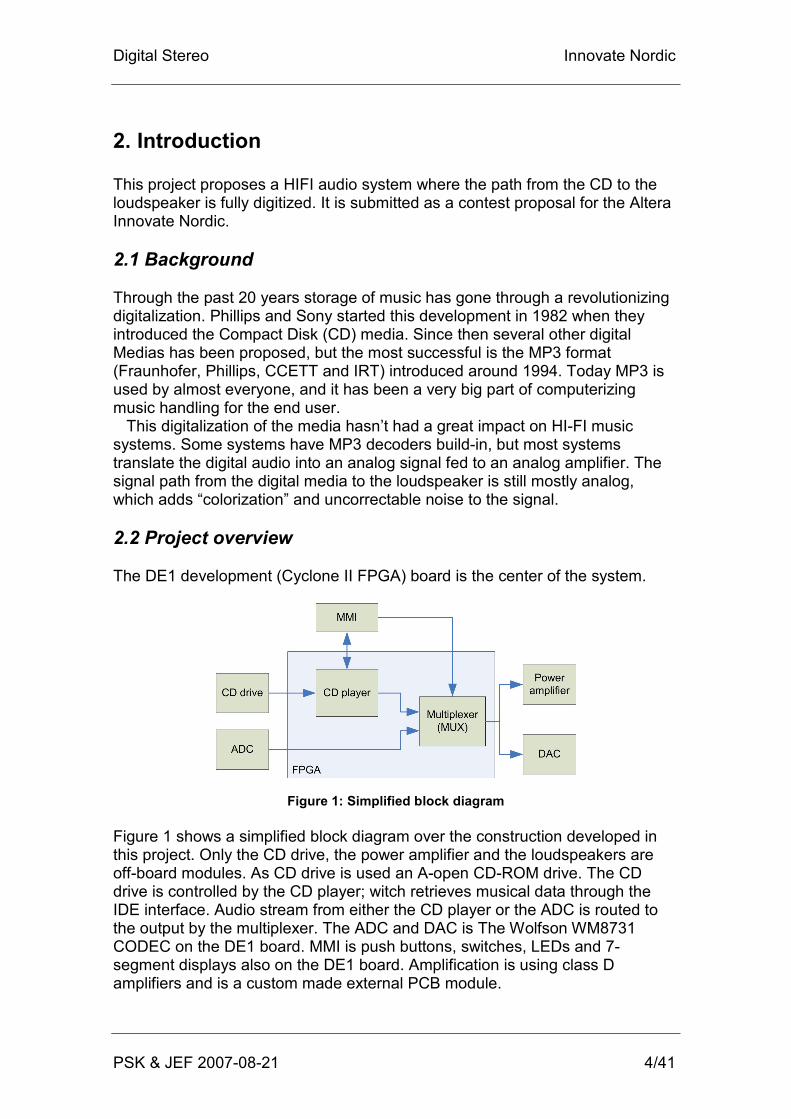
2. Introduction This project proposes a HIFI audio system where the path from the CD to the loudspeaker is fully digitized. It is submitted as a contest proposal for the Altera Innovate Nordic. 2.1 Background Through the past 20 years storage of music has gone through a revolutionizing digitalization. Phillips and Sony started this development in 1982 when they introduced the Compact Disk (CD) media. Since then several other digital Medias has been proposed, but the most successful is the MP3 format (Fraunhofer, Phillips, CCETT and IRT) introduced around 1994. Today MP3 is used by almost everyone, and it has been a very big part of computerizing music handling for the end user. This digitalization of the media hasn’t had a great impact on HI-FI music systems. Some systems have MP3 decoders build-in, but most systems translate the digital audio into an analog signal fed to an analog amplifier. The signal path from the digital media to the loudspeaker is still mostly analog, which adds “colorization” and uncorrectable noise to the signal. 2.2 Project overview The DE1 development (Cyclone II FPGA) board is the center of the system.
Figure 1: Simplified block diagram
Figure 1 shows a simplified block diagram over the construction developed in this project. Only the CD drive, the power amplifier and the loudspeakers are off-board modules. As CD drive is used an A-open CD-ROM drive. The CD drive is controlled by the CD player; witch retrieves musical data through the IDE interface. Audio stream from either the CD player or the ADC is routed to the output by the multiplexer. The ADC and DAC is The Wolfson WM8731 CODEC on the DE1 board. MMI is push buttons, switches, LEDs and 7-segment displays also on the DE1 board. Amplification is using class D amplifiers and is a custom made external PCB module.

Digital Stereo Innovate Nordic
PSK & JEF 2007-08-21 5/41
A photograph of the project hard ware can be seen on Figure 2.
Figure 2: Photograph of prototype
In the photograph isn’t shown the SMD side of the PCB. It can be seen in the chapter about the power amplifier. The external modules are connected to the DE1 board through ribbon cables. The CD-ROM IDE interface pins have to be rerouted to fit the GPIO connector (JP1) on the DE1 board. This is why the “GPIO↔IDE interface board” is necessary. 2.3 Development responsibilities The development work has been divided in the group. Jens has been working on the Class D amplifier hardware and the design of the audio processing system. Peter has been working on the CD-Rom interface and on retrieving the audio data from the CD.
Digital Stereo Innovate Nordic
PSK & JEF 2007-08-21 6/41
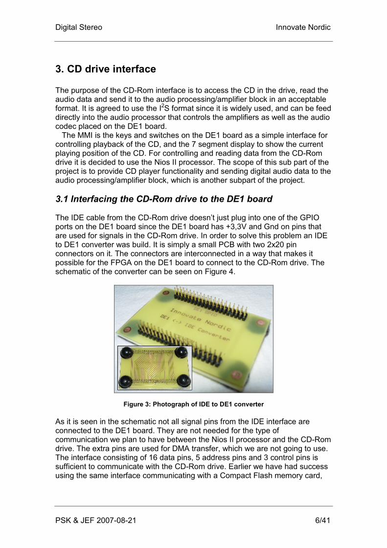
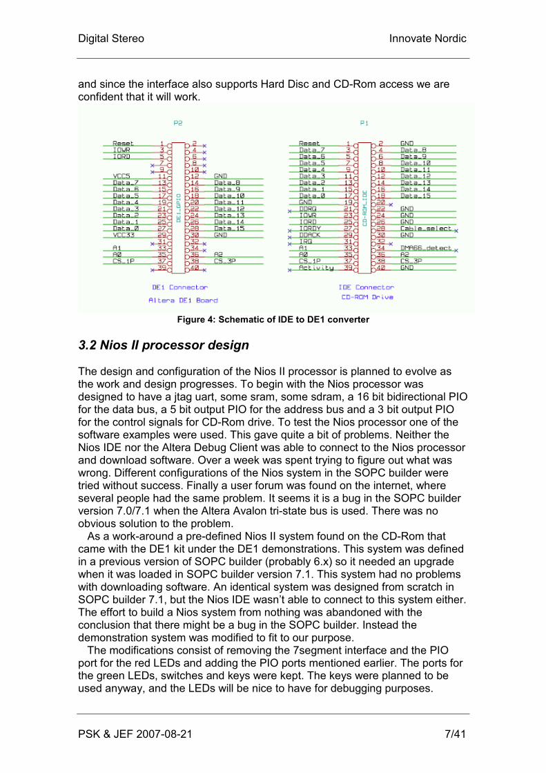
3. CD drive interface The purpose of the CD-Rom interface is to access the CD in the drive, read the audio data and send it to the audio processing/amplifier block in an acceptable format. It is agreed to use the I2S format since it is widely used, and can be feed directly into the audio processor that controls the amplifiers as well as the audio codec placed on the DE1 board. The MMI is the keys and switches on the DE1 board as a simple interface for controlling playback of the CD, and the 7 segment display to show the current playing position of the CD. For controlling and reading data from the CD-Rom drive it is decided to use the Nios II processor. The scope of this sub part of the project is to provide CD player functionality and sending digital audio data to the audio processing/amplifier block, which is another subpart of the project. 3.1 Interfacing the CD-Rom drive to the DE1 board The IDE cable from the CD-Rom drive doesn’t just plug into one of the GPIO ports on the DE1 board since the DE1 board has +3,3V and Gnd on pins that are used for signals in the CD-Rom drive. In order to solve this problem an IDE to DE1 converter was build. It is simply a small PCB with two 2x20 pin connectors on it. The connectors are interconnected in a way that makes it possible for the FPGA on the DE1 board to connect to the CD-Rom drive. The schematic of the converter can be seen on Figure 4.
Figure 3: Photograph of IDE to DE1 converter
As it is seen in the schematic not all signal pins from the IDE interface are connected to the DE1 board. They are not needed for the type of communication we plan to have between the Nios II processor and the CD-Rom drive. The extra pins are used for DMA transfer, which we are not going to use. The interface consisting of 16 data pins, 5 address pins and 3 control pins is sufficient to communicate with the CD-Rom drive. Earlier we have had success using the same interface communicating with a Compact Flash memory card,
Digital Stereo Innovate Nordic
PSK & JEF 2007-08-21 7/41
and since the interface also supports Hard Disc and CD-Rom access we are confident that it will work.
Figure 4: Schematic of IDE to DE1 converter
3.2 Nios II processor design The design and configuration of the Nios II processor is planned to evolve as the work and design progresses. To begin with the Nios processor was designed to have a jtag uart, some sram, some sdram, a 16 bit bidirectional PIO for the data bus, a 5 bit output PIO for the address bus and a 3 bit output PIO for the control signals for CD-Rom drive. To test the Nios processor one of the software examples were used. This gave quite a bit of problems. Neither the Nios IDE nor the Altera Debug Client was able to connect to the Nios processor and download software. Over a week was spent trying to figure out what was wrong. Different configurations of the Nios system in the SOPC builder were tried without success. Finally a user forum was found on the internet, where several people had the same problem. It seems it is a bug in the SOPC builder version 7.0/7.1 when the Altera Avalon tri-state bus is used. There was no obvious solution to the problem. As a work-around a pre-defined Nios II system found on the CD-Rom that came with the DE1 kit under the DE1 demonstrations. This system was defined in a previous version of SOPC builder (probably 6.x) so it needed an upgrade when it was loaded in SOPC builder version 7.1. This system had no problems with downloading software. An identical system was designed from scratch in SOPC builder 7.1, but the Nios IDE wasn’t able to connect to this system either. The effort to build a Nios system from nothing was abandoned with the conclusion that there might be a bug in the SOPC builder. Instead the demonstration system was modified to fit to our purpose. The modifications consist of removing the 7segment interface and the PIO port for the red LEDs and adding the PIO ports mentioned earlier. The ports for the green LEDs, switches and keys were kept. The keys were planned to be used anyway, and the LEDs will be nice to have for debugging purposes.

Digital Stereo Innovate Nordic
PSK & JEF 2007-08-21 8/41
As the development progressed, the Nios II processor was expanded. An interval timer was added to provide interrupts for polling the keys that became the control interface for the CD player. Additional PIO ports were added for sending audio data. These PIO ports include two 24bit output busses, one for each audio channel. The CD audio is only 16 bit, but some CD’s are recorded in 20 bit, and DVD’s are 24 bit, so it seemed reasonable to make the system capable to handle 24 bit data. The only changes needed to support this are software. The parallel audio data is converted into I2S format by a VHDL design outside the Nios processor. This design has a reset and an enable input as well as a ready output that toggles when the converter is ready for new data. These signals are also connected to the Nios processor through PIO ports. The ready PIO port has an edge triggered interrupt. This is used to make sure that audio data will be present at the audio output busses.
Figure 5: Nios II Processor System block diagram
A 28 bit PIO output port for controlling the 7 segments on the board was added. By controlling the 7 segments by software alone any of the LEDs in the segments can be switched on or off individually (If one wishes to). For testing of the CD player block the audio codec on the DE1 board will be perfect. The codec is controlled by an I2C interface. For easy control of the codec the clock and data signals are implemented as PIO ports in the Nios

Digital Stereo Innovate Nordic
PSK & JEF 2007-08-21 9/41
processor. The clock line as output and the data line as a bidirectional port. The complete Nios II processor system can be seen on Figure 6 and as block diagram on Figure 5.
Figure 6: Nios II configuration

Digital Stereo Innovate Nordic
PSK & JEF 2007-08-21 10/41
3.3 ATA/ATAPI interface The communication protocol for the ATA/ATAPI interface is described in the standards published by the T13 group at www.t13.org . Here ATA/ATAPI-4 (d1153r18) was used. For communicating with the CD-Rom drive a different standard was used. At first the obsolete SSF-8020i was used because it has a very good description of the inner workings of the CD-Rom drive. Afterwards the Multi Media Command Set standard (mmc2r11a) from the T10 group at www.t10.org was used. It is not necessary to use a newer version of the standards, because the changes made in the standards only affects newer technologies. The newer versions of the MMC standards include support for CD writers, Blue Ray etc. This is not needed for this project and the MMC2 document is significantly smaller than the later versions. First step in the development of the interface was hardware interface at the lowest level. This is what is described in the ATA/ATAPI-4 standard. The communication through the ATA interface is performed through 8 bit registers addressed with the 3 address and 2 chip select signals. These signals are the 5 bit address PIO on the Nios processor. Only one of the chip select signals can be active at the time. This makes 16 possible register addresses where only 9 are used. The reading from and writing to the registers are done with a read and a write signal. These signals are in the control PIO on the Nios processor who also contains a reset signal to the CD-Rom drive. The 8 bit register is bit 7 to 0 on the 16 bit data bus. The 9 registers are called the task file. These are used to control the connected device. The task file of a data read/write register, error, status, feature, command register and a few other registers. The short version of the way it works is that commands on the device are performed by writing a byte to the command register. The command the device performs depends on the byte written to the command register. If the command need parameters to run these are written to the rest of the task file registers. The commands available and the parameters they take can be found in the ATA/ATAPI-4 standard. It is very well documented. The most basic functionality for the interface is programmed in the hw_interface.c and hw_interface.h files (See the source code). They contain functions for reading from and writing to the registers in the task file and functions to initialize and reset the interface. For convenience there is also made a function that reads the value of the busy bit in the status register. It is quite easy to get the busy bit from the status register. The only reason that this has its own function is that it is used very often. On top of the simple basic functions are the real ATA and ATAPI commands. As described in the MMC-2 ATAPI (or ATA Packet Interface) is an extension of ATA that allows SCSI devices to be connected to the ATA interface. The standard ATA interface is usually used by disk drives but Compact Flash cards supports the ATA interface as well. ATAPI is normally used by CD/DVD Rom drives. The ATAPI protocol works by first sending an ATA command called ”ATAPI packet command” having the command byte A0h. Following this a packet of 12 bytes are send as data containing the packet command and the parameters for

Digital Stereo Innovate Nordic
PSK & JEF 2007-08-21 11/41
the command. The device will then try to perform the command. If it fails an error is indicated in the status register. If the command is successful no error is indicated and if the command returns data the number of bytes to read from the device is available in two of the task file registers. The commands available and their parameters can be found in the Multi Media Command Set (MMC) standard. The standard is very well written, and the protocols for different ATAPI transfers are shown in detail. The programming of the ATAPI software was unproblematic. The biggest challenge was getting an overview of the ATA/ATAPI-4 and the MMC-2 standards and sorting out which of the many commands are relevant for this project. ATA and ATAPI commands used in this project can be found in ATAPI.h and ATAPI.c. Not all of the ATA and ATAPI commands in the files are used in the final project, but they have been necessary during the development of the ATAPI interface software. The CD-Rom drives used in this project are taken from an old computer. It had an old AOPEN x52 speed CD-Rom drive and a Creative CD writer. Both drives have been used during the development process.
Figure 7: CD-ROM drives used in the project
The capabilities of the drives were not know. Therefore some of the first commands written were the “Identify Device” and “Inquiry” commands. The first command returns information on the serial number, firmware revision, model number and electrical timing. The last command returns information on which standards the device conforms to, and various vendor and product information. In order to get an idea of which data formats are supported and the hardware capabilities of the drive another ATAPI command was needed. The command “Mode Sense” has the ability to return a data packet (Called a page) containing CD-Rom capabilities and mechanical status. By reading this page it was verified that both drives support CDDA read operations. This means that the digital

Digital Stereo Innovate Nordic
PSK & JEF 2007-08-21 12/41
audio data can be read directly from the CD. This wasn’t the plan to begin with. At first the intention was to make the CD-Rom drive play the CD, and take the digital output from the connector on the rear side of the drive and feed it to the audio processing/amplifier stage. This was abandoned but more on that later. The ATAPI commands to read status and capabilities information from the drive were a good way to test if the ATAPI interface software was working, and to build a good skeleton for implementing more commands. After successful test of the first ATAPI commands several others were implemented in order to be able to play, pause and stop the CD. These functions were implemented and tested with success. To read the number of audio tracks, their length and the total length of the CD the Read TOC (Table of content) ATAPI command was implemented. The data received are processed by the functions in the TOChandler.h and TOChandler.c. These functions are described in the TOC handler section of this document. The ATAPI functions implemented at this time were sufficient to begin making the basic CD player functionality. Consult the CD player functionality section in this document for further details on that subject. Several other ATAPI commands are implemented. They are not that interesting. The way the ATAPI commands are send comes in two variations. One that returns data and one that doesn’t. The only difference in the different commands are the setup of the packet before it is send to the CD-Rom drive. 3.4 CD player functionality The basic CD player must contain a minimum of functions. This includes play, pause, stop, eject and skip to next and previous audio track. A lot of other features could be implemented, but since only four keys are available for control it is better to keep the interface simple. The function of the keys can be seen in the table below.
Key # Functionality 1 Skip to next track 2 Skip to previous track 3 Play, Pause 4 Stop, Open/close CD tray
The functionality of the CD player is implemented as a state machine with six states. The states are: Check for CD, Ready, Not Ready, Tray Open, Playing and Paused. The sequence of the states and which events cause which transition can be seen on Figure 8. After Power up general initialization is performed, and the state machine loop is entered. The relevant code for the current state are executed, and if an event that can cause a change in state it is changed accordingly. In the Check for CD state it is attempted to read the TOC from the CD. If a TOC is successfully read it is written to the console via the jtag uart and the state changes to Ready. If it after several attempts fails to read the TOC the Not Ready state is entered.

Digital Stereo Innovate Nordic
PSK & JEF 2007-08-21 13/41
In the Not Ready state the only allowed action is to eject the CD tray and load a new disk. When the CD tray is ejected the state changes to Tray Open.
Figure 8: CD player State Machine
The Tray Open state does nothing. It only waits until the eject button is pressed, which initiates the closing of the CD tray, and changes the state to Check for CD. If the current state is Ready it indicates that the CD is ready to be played, and the current position of the CD is at the beginning of the first track. Nothing is performed in this state until the play button is pressed starting playback of the CD and changing the state to Playing, or the eject button is pressed causing the tray to open and changing the state to Tray Open. If the state is Playing all the keys have a function, but only two of them will change the state of the state machine. If the stop button is pressed the state changes to Ready, The audio playback is stopped and the current position on the CD is set to the beginning of the first track. If the pause button is pressed the audio playback will be stopped, but the current position on the CD when paused is kept in order to be able to resume playing from the same position. If the skip to next track button if pressed the current position on the CD is set to the beginning of the next track. If the current track is the last one on the CD the current position is set to the beginning of the first track. If the skip to previous track button is pressed the relative position of the current track is checked. If the relative position is more than three seconds into the current track the current position in the CD is set to the beginning of the current track. If the relative position is less the three seconds into the current track the current position on

Digital Stereo Innovate Nordic
PSK & JEF 2007-08-21 14/41
the CD is set to the beginning of the track before the current track. If the current track is the first one on the CD then the current position is set to the beginning of the last track on the CD. When the state machine is in the Paused state the buttons have almost the same function as in the Playing state. The only exceptions are that the play button resumes audio playback and changes the state to Playing. The two skip buttons and the Stop button have the exact same function as in the Playing state. Every time the state machine loop has been executed the 7-segment displays are updated depending of the current state of the state machine. If the state is either Playing or Paused the current (absolute) position on the CD, the relative position of the current track or the number of the current track can be displayed. What information to display is chosen by the position of some of the switches on the DE1 board. If the state machine is in the Playing state a bit of code is executed every time the main loop is run. This has to do with the audio playback, and updating the content of some data buffers. This will be described in detail in the section about the audio transmitter. The CD player main loop seems to function alright. It hasn’t been subject to extensive testing, but during the development process of the project it has been used quite a lot, an a few bugs has been found and corrected. The current CD player interface is very limited, and is only intended to use as a proof of concept interface. The final version should contain more keys for the control interface, and a different kind of display. Maybe a character or graphic LCD display. The extended control interface should make it possible to implement more advanced features. Some of the features could be repeat track, repeat disc, random track play, program track sequence, etc. This must wait until version 2 of the project. 3.5 Audio transmitter The initial idea in the development of the CD player part of the project was to start the audio playback on the CD-Rom drive and route the digital audio output from the rear side of the drive to the audio processing/amplifier block. Once the audio playback is started the CD-Rom drive pretty much takes care of it self. That was one of the very appealing properties of this approach. This idea proved to be a bit harder to implement than first estimated. The format of the digital output is SPDIF. It is significantly different from the I2S format that is needed by the audio processing/amplifier block. A SPDIF to I2S converter could be constructed, but only one of the two CD-Rom drives used for this project had a SPDIF output. Because of that the design was reconsidered. The new design idea is to read the audio data from the CD and sending them to a parallel to I2S converter implemented in VHDL outside the Nios II processor. The I2S bus transmits data at 64 times the sampling frequency of the audio data. This creates a requirement for data being available in a steady stream. The I2S converter is constructed in such a way that it toggles a signal when the parallel data has been read and the converter is ready for a new set of audio samples. To insure that data is always present for the I2S converter an interrupt

Digital Stereo Innovate Nordic
PSK & JEF 2007-08-21 15/41
function is set up to trigger on every edge received on the Ready pin in the Audio Transmitter block in the Nios processor. The interrupt function has access to two large buffers. They will be full of audio data. While one buffer is being transmitted to the I2S converter the other buffer is being filled with data from the CD-Rom drive. Audio data read from the CD is read in frames of 2352 bytes. Since the audio data is stereo and has a resolution of 16 bits each block contains 588 samples, with a sampling frequency of 44100 Hz a frame of data will take 1/75th of a second. This leads to the MSF structure/format used to address data on the CD. The MSF structure consist of three bytes named M, S and F. M indicated minutes, S is seconds and can hold the values zero to 59, F is frames and can hold the values from zero to 74. The two buffers containing audio data can hold 30 frames each. Each buffers length in time is 400 ms. The time needed for the CD-Rom drive to fill the buffer is approximately 150 ms. This leaves plenty of time for the processor to perform other tasks. The length of the two buffers can be set to other values, but a length of 30 frames seemed to work fine, and there was no need to change this setting. Two state variables are associated with each of the buffers. They are used to tell the interrupt function if the buffers are ready to be played, and the section of code in the main loop (mentioned earlier) which buffer is ready to be filled with new audio data. The section of code in the main loop checks the state of the two buffers. If one is empty it is loaded with data, and its state is changed to ready. The interrupt function has an index pointer telling how far along in the buffer the playback is. When the index pointer reaches the end of the buffer, the state of the buffer is changed to empty making it possible for the main loop to fill it with new data. If the other buffer is ready the interrupt function switches to this buffer, resets the index pointer and sets the state of the now selected buffer to playing. If the second buffer isn’t ready when the first buffer has been processed, it is assumed that the end of the CD has been reached. In this case both buffer states are set to empty. Along with the interrupt function there are a few other functions in the AudioTransmit.h and AudioTransmit.c. These functions are primarily used to read and write to the private variables of the AudioTransmit functions group. There are also functions for initialization and control functions for the I2S converter. They can reset, enable/disable the vhdl module. Reset returns the I2S converter to the initial state. If the enable signal is active data is read form the left and right data bus and transmitted on the I2S bus. If enable is inactive the audio data is disregarded and the converter transmits zero values. 3.6 Table of Contents (TOC) handler To process the TOC data read from the CD a set of functions has been written in a grouping called TOChandler. These are found in TOChandler.c and TOChandler.h. Since the length of the TOC varies with the number of tracks on the CD the memory for storing the TOC is dynamically allocated. The setTOC function gets a pointer to where the TOC data from the CD is located, and an unsigned short telling the number of bytes in the TOC data. The function then

Digital Stereo Innovate Nordic
PSK & JEF 2007-08-21 16/41
allocated the needed memory, and organizes the TOC information in a way that is easily accessible for further use. A data structure called MSF_type is defined in the TOChandler function set. It is used to contain position indexes on the CD in the MSF format mentioned earlier. The TOChandler group also includes functions to reset the TOC and free the allocated memory, to tell if a valid TOC is present and to retrieve various information from the TOC. This includes the number of tracks and length of the CD, the position of a given tracks beginning, and the current track number calculated from the current position on the CD. Further more there are a few functions to perform basic math and comparison operations on the MSF_type data structure. 3.7 Keypad The control interface for the CD player is based on the keys on the DE1 board. The type of keys used has in previous projects proved to generate a lot of contact bouncing. Although debounced on the DE1 board it is further eliminated by combining polling with counters with hysteretic thresholds for each of the keys. It works by polling the keys and updating counters depending on the state of the keys. If a key is pressed the counter is incremented otherwise it is decremented. The counters are limited to a certain value range. The range can vary with the type of key used and the polling interval of keys. Upper and lower thresholds are set to suitable values within the counter range. If the upper threshold is exceeded the state of the key is considered active, if the counter value goes below the lower threshold the key state is considered inactive. This method has proven successful in previous implementations on embedded systems. And it worked quite well here too. The polling function is triggered by a 1 ms interval timer interrupt. To check if a key has been pressed a function called pressedKeypad is used. This function returns a bit pattern corresponding to the pressed keys. Once read the bit pattern is reset until the key has been released and is pressed again. The polling function is triggered by the timer interrupt repeatedly during program execution. The pressedKeypad function is called in the beginning of every main loop cycle. 3.8 Display To control the four 7-segments a setDisplay function is used. It takes a string as parameter, and writes the supported characters to the 7-segments. If a character is not supported the 7-segment is left blank. The characters that are supported are all the numbers and the “-“ sign. The display is quite easy to use by first forming a string with the spritf function from the stdio.h library. 3.9 CD-Text CD-text is text information stored in the CD. This can contain the name of the CD, the recording artist, track names etc. Not all CD’s contain this information, and not all CD-Rom drives support reading this information. Only one of the

Digital Stereo Innovate Nordic
PSK & JEF 2007-08-21 17/41
drives used in this project had CD-text support. Just to se if it was possible CD-text was support was implemented. It functions almost in the same way as the TOChandler. An initCDTEXT function is called with a pointer to the CD-text data from the CD, the size of the CD-text data in bytes and the number of tracks on the CD. The needed amount of memory is allocated, and the track titles and artist names are sorted out, and placed in memory for later retrieval. The getCDTEXTtitle and getCDTEXTartist functions takes a tracknumber as parameter and returns a pointer to the appropriate string. The CD-Text support has no crucial function, but it is a neat little feature. 3.10 I2S converter In order to be able to send data in the right format to the audio processing/amplifier block it was necessary to design a parallel to I2S converter. The design is made in VHDL. It takes parallel data form to 24 bit busses, and sends it out on an I2S bus. The design creates all the necessary clock signals for the I2S bus, but needs a master clock signal that is a multiple of 64 times the audio sampling frequency. Here 256 times FS = 11,2896 MHz is used. The clock is generated by a PLL with the 24 MHz clock on the DE1 board as input. The I2S converter schematic symbol can be seen on Figure 9. The connections on the left are inputs and those on the right are outputs. The reset is an asynchronous reset meaning that it is independent clk signal. The clk signal if divided by four internally in the converter. The divided clock signal is now equal to 64 times FS. It is routed directly SCK output. The On the falling edge of the divided clock signal data from an internal 64 bit register is shifted out on the SD output while the index of the register is less than 32 the WS output is set to zero otherwise it is set to one. When the index reaches the end of the register values from the DataL and DataR busses are latched into the register if the enable input is one. If enable is zero the register is loaded with zeros. After the register is loaded the Ready output is toggled indicating that the converter is ready for new data on the DataL and DataR busses. The SCK, WS and SD signals forms the I2S bus. SCK is the clock signal, SD data and WS the word select or left/right clock. It might seem a bit strange that two 24 bit busses are latched into a 64 bit register indexed bit 63 to 0 with 63 as the msb. The DataL bus is latched into bit 62 to 39 of the register and DataR into bit 30 to 7. This is to conform to the I2S protocol.

Digital Stereo Innovate Nordic
PSK & JEF 2007-08-21 18/41
clk
reset
enable
DataL[23..0]
DataR[23..0]
Ready
SCK
WS
SD
I2Stransmitter
inst
Figure 9: I2S converter symbol
The I2S converter design has been tested with simulated waveforms. The results of the simulation looked correct. To test even further the I2S converter was connected to the audio codec on the DE1 board. The codec is able to play the audio converted to I2S format by the converter and read from the CD. It sounded quite good actually. 3.11 Phase Locked Loops The system uses Phase Locked Loops to generate the needed clock signals. One PLL doubles the 50 MHz to a 100 MHz clock used by the Nios processor and a slightly delayed version of the 100 MHz clock used by the sram. The audio clock must be a multiple of 44100 Hz. The 24 MHz clock can be made into 22.5792 MHz which is 512 times FS.

Digital Stereo Innovate Nordic
PSK & JEF 2007-08-21 19/41
4. The Wolfson WM8731 CODEC The DE1 board is equipped with a WM8731 CODEC. In this project the CODEC is used as both test equipment for other modules and as secondary input/output for the audio system. 4.1 CODEC Hardware in this project The CODEC is mounted on the DE1 board and has fixed connections to the FPGA (hence fixed pins; refer to the FPGA pintable in the overall implementation section). Initialization of the CODEC is through a standard I2C (Inter-Integrated Circuit) bus, and sound transfer is through a 3-wire bus, witch in this project is defined as a standard I2S (Inter-IC Sound) bus. Both the I2C [1] and the I2S [2] bus is originally defined by Philips, but is now de facto standards.
Figure 10: Connection diagram of CODEC part of the DE1 board
The figure above shows the structure of the CODEC connection to the project. Pin numbers on the FPGA are marked just inside the FPGA frame. All control signals for the CODEC are generated using the NIOS II processor. Routing of the sound signals is done using VHDL modules. NOTE: Errors are encountered in the DE1 manual. On page 38, figure 4.15 the write (and read) addresses for the I2C bus is wrong. True write address is 34h. On page 39 in table 4.9 the description for the I2C bus is wrong. I2C_DATA is connected to PIN_B3 and I2C_CLOCK is connected to PIN_A3. 4.2 CODEC setup Registers of the CODEC is initialized as shown in the table below. All registers are written using slave device address 34h on the I2C bus. The sub address of this device operates with only 7bit. This deviates from the standard, witch

Digital Stereo Innovate Nordic
PSK & JEF 2007-08-21 20/41
suggest an 8bit sub address. Because of this the sub address will not be uniquely identifiable in the hexadecimal value to send. Register Sub
address 7bit
Binary setting 9bit
Hex to send
Description
R0 0000000b 000010111b 0017h R1 0000001b 000010111b 0217h
Line input amplification is 0dB and mute is disabled. Left (R0) and right (R1) input registers do not load simultaneously.
R2 0000010b 011100101b 04E5h R3 0000011b 011100101b 06E5h
Output amplification is -20dB and mute is disabled. Left (R2) and right (R3) output registers do not load simultaneously.
R4 0000100b 000010010b 0812h Connect input to ADC. No mic or bypass from input to output.
R5 0000101b 000000000b 0A00h Enable ADC high pass filter. Disregard DC level. No mute or other filtering.
R6 0000110b 001100010b 0C62h Power down: mic. ampl., oscillator and CLKOUT.
R7 0000111b 000001010b 0E0Ah Use I2S, 24bit, lrclk as in standard and CODEC is slave.
R8 0001000b 000101000b 1028h Use normal mode with fs=44.1kHz and XCLK=256fs
R9 0001001b 000000001b 1201h Activate device. R10 0001111b Reset register is not used in this application
The CODEC output volume is corrected by user intervention at runtime, otherwise all CODEC registers is only set at power on. 4.3 I2C The standard defines a master/slave based bus system. In the CODEC case the slave is the WM8731 and the master the FPGA.
Write of one byte
The protocol is shown in Figure 11. From last chapter is recognized 8bit data, 8bit sub address and a 7bit address followed by a R/W bit. In the CODEC case only writing is interesting, and these 8bits give the 34h mentioned earlier.
Figure 11: I2C protocol (from Philips I
2C specification)

Digital Stereo Innovate Nordic
PSK & JEF 2007-08-21 21/41
ACK is a low response from the slave. The protocol defines that idle of the bus is logic high. This is achieved by using pull-up resistors on the physical bus (R=2kΩ on the DE1 board), and putting outputs of slaves and masters on the bus in tristate when idle. This also means that when a device is transmitting logic high, it should tristate the output, and when low it must pull the wire to ground. In this project however logic high and low is used. This will not pose a problem.
Write of multiple bytes
Some I2C devices require the writing of several bytes for each sub address. The power amplifier circuits used I the project requires a four byte write for some of the sub addresses. There don’t seem to be basis for this kind of operation in the I2C standard but never the less it is used. Below is the impulse diagram of the SDA, the start and stop is similar to Figure 11.
Figure 12: Multiple byte write transfer (from TI datasheet TAS5504)
Read
First part of the read process is similar to the write. The master device transmit START condition, address of the slave, ‘0’ in the R/W bit. After ACK the sub address is transmitted. Here the similarities end, because a new START condition is transmitted followed by the slave address but a ‘1’ as R/W bit. Now the slave takes control of the SDA, and the master replies with ACK.
Figure 13: Read of a single byte (from TI datasheet TAS5504)
I2C signal routing in present project
Due to the DE1 hardware there is only two devices on the bus (I2C_bus_A), however the need to attach further devices have arisen in this project (the power amplifier also needs I2C bus connectivity). To overcome this problem a second pair of bus pins will be assigned the exact same signals as the I2C_bus_a. This second bus is named I2C_bus_b. This approach is chosen

Digital Stereo Innovate Nordic
PSK & JEF 2007-08-21 22/41
because the FPGA software will not allow two bidirectional wires to be connected directly.
Figure 14: Routing of I2C signals
Because of the chosen routing, the devices on either I2C_bus_a or I2C_bus_b will appear to be on the same bus. When using the send, long send and receive functions (I2C implementation in next section) the programmer will not have to distinguish between two hardware busses. A second master device on I2C_bus_b will not be able to see the I2C_bus_a though. Figure 14 shows the setup of the I2C routing. The off-board I2C bus uses GPIO socket 1 (JP2) pin 5 for SDAT and pin 8 for SCLK (pin G14 and G16 on the FPGA). Future devices on the figure are not a part of the project, but merely to show the expandability of the bus.
I2C implementation
The I2C_bus_a and I2C_bus_b hardware are generated by adding PIOs to the Avalon bus using the SOPC builder. All address configurations is also managed by the SOPC builder.
Figure 15: Snapshot of the SOPC builder of I2C hardware

Digital Stereo Innovate Nordic
PSK & JEF 2007-08-21 23/41
Addresses of the I2C hardware is shown in Figure 15, but are automatically copied to the system.h file on “make clean” command in the Nios II environment. Protocols are implemented by driving the bus to hard low or high according to the previously described. When the ACK is expected the direction of the SDA pin is reversed, if the slave pulls SDA low no error is returned, else error is indicated. The error indication is displayed in the IDE console (via JTAG), but do not affect the program in present implementation. 4.4 Test of CODEC To ensure the CODEC doesn’t corrupt test data (and audio data) the transfer function of the codec is measured. During test output amplification is set to 0dB (R2: 04F9h and R3: 06F9). In the FPGA the DACDAT is connected ADCDAT (Figure 17). Test setup is shown below.
Figure 16: Test setup
To compensate for the standard soundcard in the PC, the right output channel is patched directly to the right input channel, and the computer software (WinMLS 2004) automatically subtracts this transfer function from the one measured by the left channel. The left channel is used to measure the System under Test (SUT), namely the DE1 board. The DE1 board loaded with NIOS II code witch produces I2C, I2S clock signals and init registers in the CODEC. Part of FPGA schematics specific for the test is shown in the figure below.
Figure 17: Software for test of CODEC transfer function.
The WinMLS 2004 uses sinus sweeps to measure the transfer function.
Digital Stereo Innovate Nordic
PSK & JEF 2007-08-21 24/41
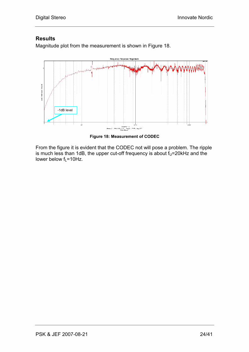
Results
Magnitude plot from the measurement is shown in Figure 18.
Figure 18: Measurement of CODEC
From the figure it is evident that the CODEC not will pose a problem. The ripple is much less than 1dB, the upper cut-off frequency is about fU=20kHz and the lower below fL=10Hz.
-1dB level
Digital Stereo Innovate Nordic
PSK & JEF 2007-08-21 25/41
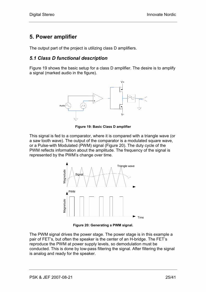
5. Power amplifier The output part of the project is utilizing class D amplifiers. 5.1 Class D functional description Figure 19 shows the basic setup for a class D amplifier. The desire is to amplify a signal (marked audio in the figure).
Figure 19: Basic Class D amplifier
This signal is fed to a comparator, where it is compared with a triangle wave (or a saw tooth wave). The output of the comparator is a modulated square wave, or a Pulse-with Modulated (PWM) signal (Figure 20). The duty cycle of the PWM reflects information about the amplitude. The frequency of the signal is represented by the PWM’s change over time.
Figure 20: Generating a PWM signal.
The PWM signal drives the power stage. The power stage is in this example a pair of FET’s, but often the speaker is the center of an H-bridge. The FET’s reproduce the PWM at power supply levels, so demodulation must be conducted. This is done by low-pass filtering the signal. After filtering the signal is analog and ready for the speaker.

Digital Stereo Innovate Nordic
PSK & JEF 2007-08-21 26/41
5.2 The triangle wave The frequency of the triangle wave must be way outside the audio signal frequency range, and always higher. If the triangle wave were equal to or had a lower frequency, the harmonics would corrupt the audio signal. The normal audible frequency range is in the interval fh=[18; 20
.103] Hz, so the switch frequency should be about fsw=30kHz. The waveform can easily be generated with a up/down counter, but to avoid degrading the audio signal by the amplifier, the solution of the triangle should be as good as the audio signal. In this project that is 24bit. This means that we need a 24bit counter that can count an up/down cycle in t=1/fsw=33.3µs or by other words, the clock supplying the counter operates at
GHzff B
swclk 3.503210302243=⋅⋅=⋅=
witch is simply not doable in a FPGA. Even if the demands are loosen there is a long way down to the maximum clock frequency of the FPGA at fmax=300MHz. This forces the PWM modulation outside the FPGA. 5.3 Texas Instruments 4 channel digital audio processor TAS5504 The TAS5504 is chosen to do the PWM modulation. Besides being able to PWM modulate 24bit at a switching frequency in the range from 32k-48k Hz it has an enormous amount of features. For this project the important features are: I2C interface for programming. I2S interface for transfer of audio signals. Four PWM channels, capable of driving four H-bridge power stages.
Figure 21: Block diagram of power amplifier
Figure 21 show the power amplifier and the connection to the DE1 board. For each power stage shown, there are two channels. This offer the possibility to move the crossover filter from the analog domain (in the speakers) to the digital domain (in the FPGA). Such configurations require an amplifier for each speaker driver (Tweeder and bass for both left and right).

Digital Stereo Innovate Nordic
PSK & JEF 2007-08-21 27/41
TAS5504 setup
There are more than 50 registers to setup in the TAS5504, so only registers that differ from the default setting is described here.
Sub address 8bit Binary setting Hex to send Description 00h 01000001b 0041h 44.1kHz sampling and master clk is 64fs D1h 00000000b
00000000b 00000000b 01000100b
D1h 00000044h
Volume of ch1 to 0dB. This register requires four data bytes.
D2h 00000000b 00000000b 00000000b 01000100b
D2h 00000044h
Volume of ch2 to 0dB. This register requires four data bytes.
D7h 00000000b 00000000b 00000000b 01000100b
D7h 00000044h
Volume of ch3 to 0dB. This register requires four data bytes.
D8h 00000000b 00000000b 00000000b 01000100b
D8h 00000044h
Volume of ch4 to 0dB. This register requires four data bytes.
D9h 00000000b 00000000b 00000000b 01000100b
D9h 00000044h
Master volume to 0dB. This register requires four data bytes.
The clock control register is automatically updated by TAS5504 auto detection, so it doesn’t really need to be initialized. 5.4 Texas Instruments Stereo Digital Amplifier Stage TAS5142 The power stage, or the backend, of the system is based on semiconductors. In the example in the beginning of this section both a P channel and an N channel MOSFET is used. Both the on and off switching time will probably be different. When both FETs are on, the current through the components will be destructive. Therefore some kind of protection is required. This project utilizes the TAS5142 Power stage. Here the protection is embedded. Further more the FETs are produced on the same piece of silicon witch reduces time differences. TAS5142 also offer over temperature detection capabilities and automatic shutdown when the temperature level is damaging.
Figure 22: TAS5142 channel A (from TI datasheet TAS5142)

Digital Stereo Innovate Nordic
PSK & JEF 2007-08-21 28/41
There are two full H-bridges in a TAS5142. Figure 21 show channel A of the power stage. TAS5142 has four of these channels. The PWM signal produced by the TAS5504 is received by the PWM receiver. Here levels and waveform are reconstructed, before latched through the control block. If the power stage is experiencing an error (power or temperature) or external reset is at logic low, the output of the block is low. Otherwise the PWM signal is latchet to the timing block. Here the PWM is split for the two FET’s and are manipulated to deal with the FET’s different switching time. Last the PWM is converted to drive signals with the high-side drivers (gate drive block). The gate drive needs a boot-strap capacitor, from GVDD to BST, to build up charge to drive the high-side of the half bridge.
Output filters
The filters needed to reconstruct the analog audio signal are suggested in the data sheet for the TAS5142.
Figure 23: Schematics of output filter
Figure 23 shows the schematics of the output filter. 5.5 Hardware for the power amplifier The overall schematics and PCB layout can be found in appendix A. This chapter discusses details in the HW design.
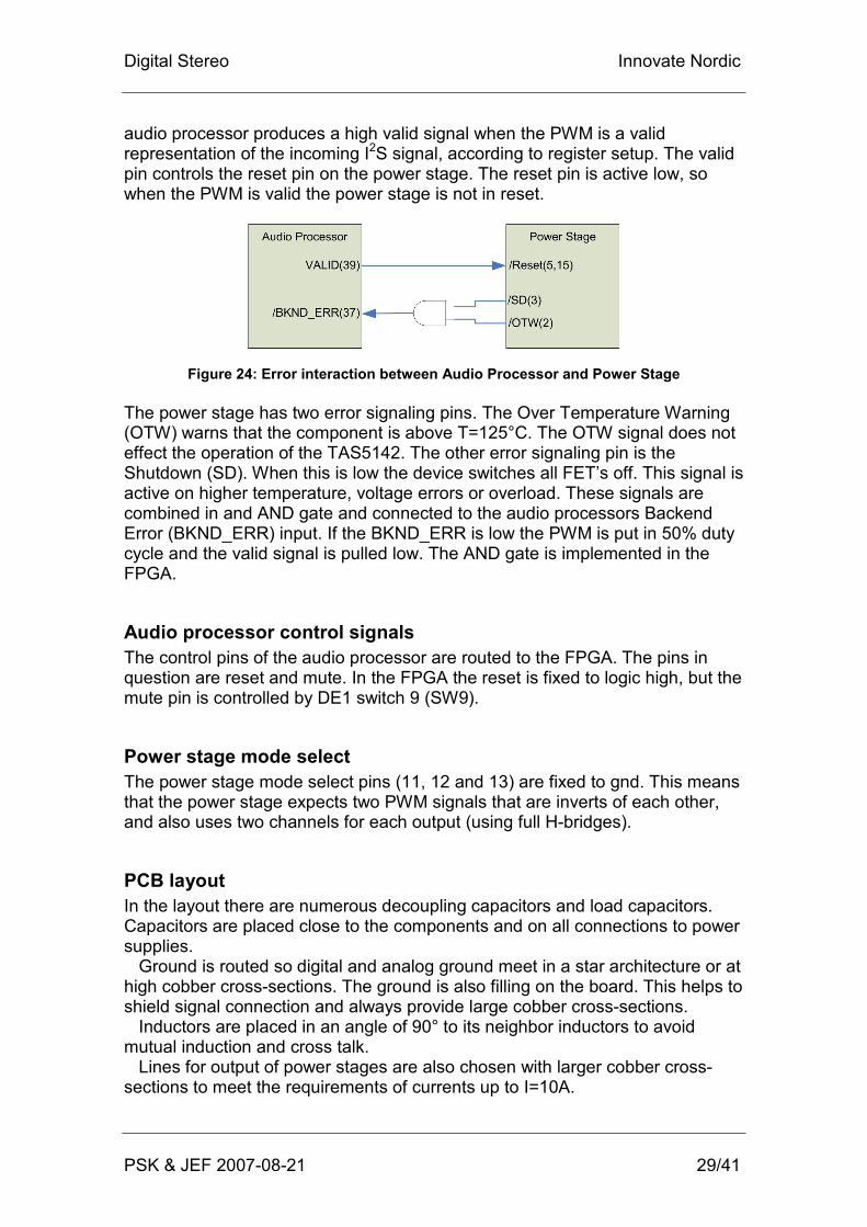
Error interaction
Figure 24 show how the audio processor and the power stage exchange error signals. Numbers in parentheses are pin numbers on actual components. The
Digital Stereo Innovate Nordic
PSK & JEF 2007-08-21 29/41
audio processor produces a high valid signal when the PWM is a valid representation of the incoming I2S signal, according to register setup. The valid pin controls the reset pin on the power stage. The reset pin is active low, so when the PWM is valid the power stage is not in reset.
Figure 24: Error interaction between Audio Processor and Power Stage
The power stage has two error signaling pins. The Over Temperature Warning (OTW) warns that the component is above T=125°C. The OTW signal does not effect the operation of the TAS5142. The other error signaling pin is the Shutdown (SD). When this is low the device switches all FET’s off. This signal is active on higher temperature, voltage errors or overload. These signals are combined in and AND gate and connected to the audio processors Backend Error (BKND_ERR) input. If the BKND_ERR is low the PWM is put in 50% duty cycle and the valid signal is pulled low. The AND gate is implemented in the FPGA.
Audio processor control signals
The control pins of the audio processor are routed to the FPGA. The pins in question are reset and mute. In the FPGA the reset is fixed to logic high, but the mute pin is controlled by DE1 switch 9 (SW9).
Power stage mode select
The power stage mode select pins (11, 12 and 13) are fixed to gnd. This means that the power stage expects two PWM signals that are inverts of each other, and also uses two channels for each output (using full H-bridges).
PCB layout
In the layout there are numerous decoupling capacitors and load capacitors. Capacitors are placed close to the components and on all connections to power supplies. Ground is routed so digital and analog ground meet in a star architecture or at high cobber cross-sections. The ground is also filling on the board. This helps to shield signal connection and always provide large cobber cross-sections. Inductors are placed in an angle of 90° to its neighbor inductors to avoid mutual induction and cross talk. Lines for output of power stages are also chosen with larger cobber cross-sections to meet the requirements of currents up to I=10A.

Digital Stereo Innovate Nordic
PSK & JEF 2007-08-21 30/41
Figure 25: SMD components on power amplifier PCB
Cooling
The TAS5142 must be equipped with an appropriate heat sink to avoid overheating. At present no calculations is made on temperature, but holes are prepared for heat sink mounting. Figure 25 only marks one of these holes, but there are four placed quadratic.
Connection to the DE1 module
The power amplifier PCB is connected to the DE1 module GPIO port 1 (JP2). While the CD drive is connected trough a standard IDE ribbon cable, the power amplifier has to be connected through an ATA ribbon cable. The difference between these two cables is that every second line in the ATA cable is a ground connection. This shields the signal lines from ambient noise and more important from cross talk. Cross talk was found to be a problem when the ordinary IDE connection was used.
I2C pull up resistors
Pull up resistors on the I2C bus is placed on the power amplifier PCB. To sink as little current as possible, the pull up resistors is chosen to R=200kΩ (16.5µA @ Vcc=3.3V). This posed a problem though. The resistors could not raise the I2C bus to logic high sufficiently fast, when the bus is tri-stated.

Digital Stereo Innovate Nordic
PSK & JEF 2007-08-21 31/41
In the present project this isn’t a problem, because the I2C masters violates the standard by pulling the bus to hard high (and do not tri-states the bus) when logic high is needed.
PCB power supply
The logic power Vcc=3.3V for the PCB is supplied from the DE1 board through the GPIO connector (JP2, pin 29). Power to drive the speakers PVDD=30V is supplied from a LAB power supply directly to the power amplifier board (screw terminals). 5.6 Test of power amplifier module There are two paths there should be testes. The first is the I2C bus for setting up the audio processor. The second is the audio path.
Test of control structure
First test is to ensure the ability to communicate with the audio processor via I2C. The I2C routine confirms that the device answers the transmission with ACK (logic low). Second register 01h (General Status Register) is read and the chip identification code is confirmed with the datasheet. Last 00h is first written to register 02h (Error Status Register). This reset sticky errors that might be obsolete, and then register 02h is read to ensure no errors occur. Unfortunately there is an error: “PLL auto lock error”. This error is fatal, and prevents the processor from producing PWM. The course of the problem is at deadline not found, so the power amplifier does not work.
Test of audio path
This is obviously not possible due to the faults found in the audio processor PLL. But a transfer function would have been obtained similar to that of the CODEC.

Digital Stereo Innovate Nordic
PSK & JEF 2007-08-21 32/41
6. Multiplexing and miscellaneous Figure 26 show VHDL modules described in this chapter.
Figure 26: Routing of audio signal and level meter
The important part of the figure is the I2S_mux. This is the audio multiplexer. To the left is the I2S_receive there converts the I2S to parallel data. The level_meter is indicating level of action on the parallel bus. 6.1 Audio multiplexer Details of the audio multiplexer are shown on Figure 27.
Figure 27: Details of the I2S_MUX
On a positive clock edge a low EN_1 will select SDAT_2 otherwise SDAT_1 will be selected. EN_1 is directly controlled by SW9 on the DE1 board. The output of the multiplexer is always routed to the CODEC, the power amplifier and to the I2S/par converter. 6.2 I2S to parallel converter Figure 28 show the functional simulation of the I2S to parallel converter (i2s_recieve). The lower three sequences are internal signals. The signal LD is generated to mark a level shift in the LRCLK. The generation of the signal is generated as follows:
1−⋅⊕= zLRCLKLRCLKLD
Where ⊕ is the “exclusive or” operator and the z-1 is a unity delay.
Digital Stereo Innovate Nordic
PSK & JEF 2007-08-21 33/41
The operation is triggered by the SCLK. This means that difference in the LRCLK from one positive SCLK edge to the next is detected.
Figure 28: Functional simulation of i2s_recieve
LRCLK difference is indicated by a high LD. When LD is high the input_buffer is copied to the respective output. This is indicated by arrows in the figure. When LRCLK is low the input_buffer contains left data, else the data is from the right channel. Filling of the input_buffer is done from the first positive SCLK edge after the LD goes low, and 24bits ahead. The input_buffer is indexed by the sclk_count signal. In the simulation the SDAT is random data. It is shown that the output data is indeed equal to SDAT in the described interval. 6.3 Level meter The level meter is producing a visual effect and can be used as a diagnostics tool. The meter is comparing positive audio values (MSB is low) to a fixed number and then turning red LED’s on according to the value. The concept is illustrated in Figure 29.
Figure 29: Level meter concept
Numbers in the columns refer to the reds LED on the DE1 board. The values compared to are chosen only on the basis of “what looks good”, and are not necessarily linear. Only comparison on every 10th sample is performed.
Digital Stereo Innovate Nordic
PSK & JEF 2007-08-21 34/41
7. Conclusions Development of the digital stereo is complete. Unfortunately the class D power amplifier is failing. The exact reasons for this are still uncovered. PCB, hardware setup and soft setup are examined and no apparent reasons are found. Århus, Denmark the 21. of August 20, 2007 and the project is ended.
8. Further development The project continues. Next step (aside from fixing the class D problem) is to digitize the crossover filters. Also the amplifiers are considered moved to the loudspeakers. If this is done, the possibility to network the speakers with each other and other devices comes naturally. Also other input devices are a natural extension to the project.

Digital Stereo Innovate Nordic
PSK & JEF 2007-08-21 35/41
A Electrical drawings
IDE ↔ DE1 interface schematics
IDE ↔ DE1 interface PCB layout

Digital Stereo Innovate Nordic
PSK & JEF 2007-08-21 36/41
Power amplifier schematics

Digital Stereo Innovate Nordic
PSK & JEF 2007-08-21 37/41

Digital Stereo Innovate Nordic
PSK & JEF 2007-08-21 38/41

Digital Stereo Innovate Nordic
PSK & JEF 2007-08-21 39/41
Power amplifier PCB layout

Digital Stereo Innovate Nordic
PSK & JEF 2007-08-21 40/41
VCC
CODEC_adcdat
INPUT
VCC
SW[7..0]
INPUT
VCC
TDI
INPUT
VCC
TCK
INPUT
VCC
TCS
INPUT
VCC
SW[9]
INPUT
VCC
SW[8]
INPUT
VCC
KEY[3..0]
INPUT
VCC
CLOCK_50MHz
INPUT
VCC
CLOCK_24MHz[1..0]
INPUT
CODEC_XCLK
OUTPUT
AMPL_MCLK
OUTPUT
AMPL_mute
OUTPUT
CODEC_DACDAT
OUTPUT
AMPL_SDAT
OUTPUT
CODEC_BCLK
OUTPUT
CODEC_ADCLRCLK
OUTPUT
CODEC_DACLRCLK
OUTPUT
AMPL_SCLK
OUTPUT
AMPL_LRCLK
OUTPUT
DRAM_ADDR[11..0]
OUTPUT
DRAM_LDQM
OUTPUT
DRAM_UDQM
OUTPUT
DRAM_CAS_N
OUTPUT
DRAM_RAS_N
OUTPUT
DRAM_CS_N
OUTPUT
DRAM_BA_0
OUTPUT
DRAM_BA_1
OUTPUT
DRAM_CLK
OUTPUT
DRAM_CKE
OUTPUT
FL_ADDR[21..0]
OUTPUT
FL_WE_N
OUTPUT
FL_RST_N
OUTPUT
FL_OE_N
OUTPUT
FL_CE_N
OUTPUT
SRAM_ADDR[17..0]
OUTPUT
SRAM_UB_N
OUTPUT
SRAM_LB_N
OUTPUT
SRAM_WE_N
OUTPUT
SRAM_CE_N
OUTPUT
SRAM_OE_N
OUTPUT
CODEC_I2C_SCLK
OUTPUT
AMPL_I2C_SCLK
OUTPUT
TDO
OUTPUT
CD_ADDRESS[4..0]
OUTPUT
CD_CTRL[2..0]
OUTPUT
DRAM_WE_N
OUTPUT
LEDG[7..0]
OUTPUT
DISPLAY[27..0]
OUTPUT
LEDR[9..0]
OUTPUT
AMPL_Reset
OUTPUT
AMPL_shutdown
OUTPUT
VCC
DRAM_DQ[15..0]
BIDIR
VCC
FL_DQ[7..0]
BIDIR
VCC
SRAM_DQ[15..0]
BIDIR
VCC
CODEC_I2C_SDAT
BIDIR
VCC
AMPL_I2C_SDAT
BIDIR
VCC
CD_DATA[15..0]
BIDIR
SDAT_1
SDAT_2
EN_1
clk
SDAT
I2S_MUX
inst1
sclk
lrclk
sdat
left_dat[23..0]
right_dat[23..0]
i2s_receive
inst39
left_dat[23..0]
right_dat[23..0]
clk
led[9..0]
level_meter
inst45
VCC
CLOCK_24[1..0]
CLOCK_50
KEY[3..0]
SW[7..0]
TDI
TCK
TCS
LEDG[7..0]
DRAM_ADDR[11..0]
DRAM_LDQM
DRAM_UDQM
DRAM_WE_N
DRAM_CAS_N
DRAM_RAS_N
DRAM_CS_N
DRAM_BA_0
DRAM_BA_1
DRAM_CLK
DRAM_CKE
FL_ADDR[21..0]
FL_WE_N
FL_RST_N
FL_OE_N
FL_CE_N
SRAM_ADDR[17..0]
SRAM_UB_N
SRAM_LB_N
SRAM_WE_N
SRAM_CE_N
SRAM_OE_N
I2C_SCLK_A
I2C_SCLK_B
TDO
ADDRESS[4..0]
CTRL[2..0]
DISPLAY[27..0]
CLK_256FS
CLK_512FS
I2S_CLK
I2S_WS
I2S_SD
DRAM_DQ[15..0]
FL_DQ[7..0]
SRAM_DQ[15..0]
I2C_SDAT_A
I2C_SDAT_B
DATA[15..0]
CDplayer
inst
B FPGA top-level design

Digital Stereo Innovate Nordic
PSK & JEF 2007-08-21 41/41
C References
1. ANSI standard: AT Attachment with Packet Interface Extension (ATA/ATAPI), Rev.18, 1998.
2. IEC standard: Compact disk digital audio system (IEC60809), “The Red
book”, 2nd edition, 1999-02.
3. Datasheet: Texas Instruments TAS5142 Stereo Digital Amplifier Power Stage, MAY 2005.
4. Datasheet: Texas Instruments TAS5504 4 Channel Digital Audio PWM
Processor, October 2004.
5. W. Marshall Leach, Jr.: Introduction to Electroacoustics & Audio Amplifier Design, 3rd edition, Kendall/Hunt Publishing Company, 2003.
6. Maxim Application note: Class D Amplifiers: Fundamentals of Operation
and Recent Developments, Dec 2006, Note # 3977.
7. Philips manual: CDD3610 Command Specification, Version 1.2 (final), APR 2007, Ref # AHR-66-MJS-0001.
8. Small Form Factor Committee Specification: ATA Packet Interface for
CD-ROMs (SFF-8020i), Rev. 2.6, JAN 1996.