ATF697FFaerosupport.atmel.com/Atmel/Atmel-41002-ATF697... · · 2016-04-21This document describes...
46
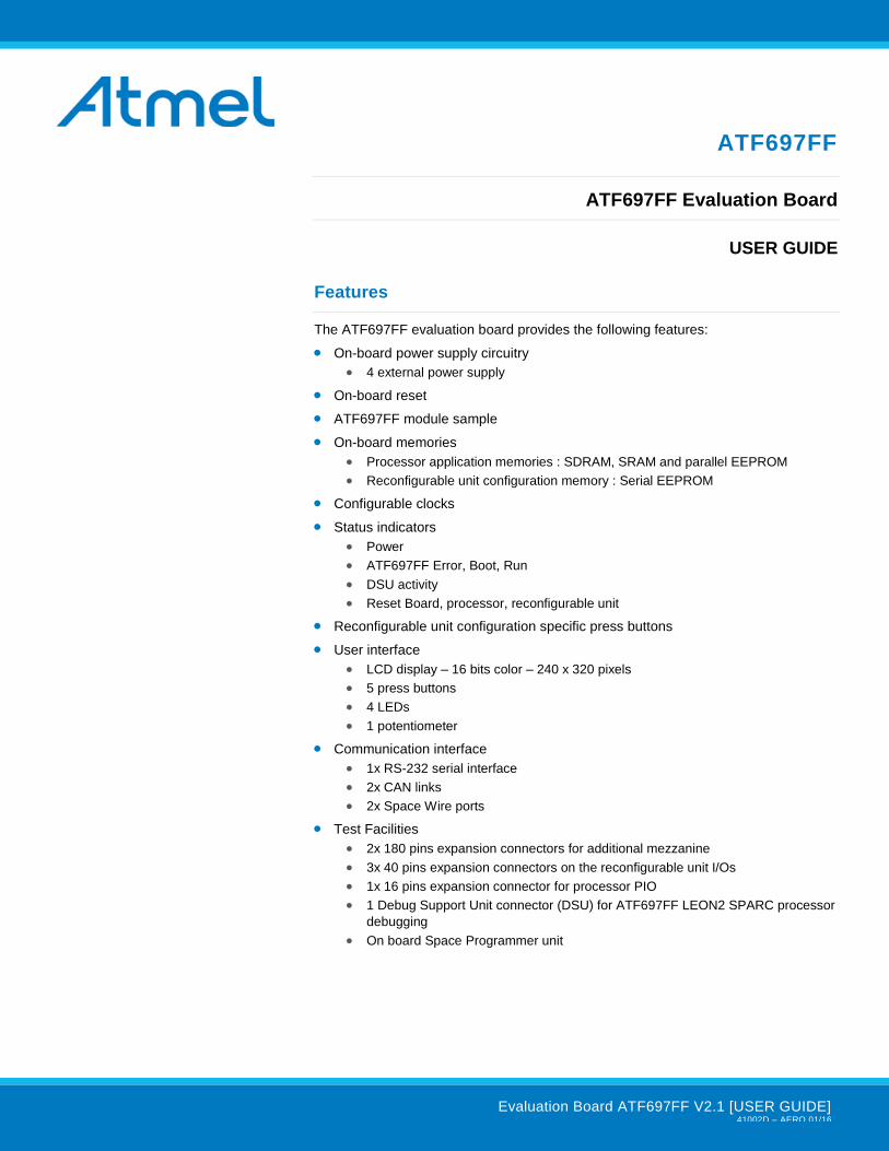
ATF697FF ATF697FF Evaluation Board USER GUIDE Features The ATF697FF evaluation board provides the following features: On-board power supply circuitry 4 external power supply On-board reset ATF697FF module sample On-board memories Processor application memories : SDRAM, SRAM and parallel EEPROM Reconfigurable unit configuration memory : Serial EEPROM Configurable clocks Status indicators Power ATF697FF Error, Boot, Run DSU activity Reset Board, processor, reconfigurable unit Reconfigurable unit configuration specific press buttons User interface LCD display – 16 bits color – 240 x 320 pixels 5 press buttons 4 LEDs 1 potentiometer Communication interface 1x RS-232 serial interface 2x CAN links 2x Space Wire ports Test Facilities 2x 180 pins expansion connectors for additional mezzanine 3x 40 pins expansion connectors on the reconfigurable unit I/Os 1x 16 pins expansion connector for processor PIO 1 Debug Support Unit connector (DSU) for ATF697FF LEON2 SPARC processor debugging On board Space Programmer unit Evaluation Board ATF697FF V2.1 [USER GUIDE] 41002D – AERO 01/16
Transcript of ATF697FFaerosupport.atmel.com/Atmel/Atmel-41002-ATF697... · · 2016-04-21This document describes...
ATF697FF
ATF697FF Evaluation Board
USER GUIDE
Features
The ATF697FF evaluation board provides the following features:
On-board power supply circuitry
4 external power supply
On-board reset
ATF697FF module sample
On-board memories
Processor application memories : SDRAM, SRAM and parallel EEPROM
Reconfigurable unit configuration memory : Serial EEPROM
Configurable clocks
Status indicators
Power
ATF697FF Error, Boot, Run
DSU activity
Reset Board, processor, reconfigurable unit
Reconfigurable unit configuration specific press buttons
User interface
LCD display – 16 bits color – 240 x 320 pixels
5 press buttons
4 LEDs
1 potentiometer
Communication interface
1x RS-232 serial interface
2x CAN links
2x Space Wire ports
Test Facilities
2x 180 pins expansion connectors for additional mezzanine
3x 40 pins expansion connectors on the reconfigurable unit I/Os
1x 16 pins expansion connector for processor PIO
1 Debug Support Unit connector (DSU) for ATF697FF LEON2 SPARC processor
debugging
On board Space Programmer unit
Evaluation Board ATF697FF V2.1 [USER GUIDE] 41002D – AERO 01/16
Evaluation Board ATF697FF V2.1 [USER GUIDE] 41002D – AERO 01/16
2
Description
This document describes the evaluation board V2.1 dedicated to ATMEL ATF697FF
configurable processor.
The ATF697FF is a multi-chip module made of an ATMEL AT697F die together with an
ATMEL ATF280F die. This allows extension of the 32-bit SPARC® V8 processor
functionalities by adding a user dedicated area made of a 280 Kgate FPGA.
The board is designed to allow an easy evaluation of the product using demonstration
software. It also provides all the features for extensive testing and application
development over the complete device by providing access to all the processor and the
reconfigurable unit signals.

Evaluation Board ATF697FF V2.1 [USER GUIDE] 41002D – AERO 01/16
3
Table of Contents
1. Overview ............................................................................................ 5
1.1 Deliverables ...................................................................................................... 5 1.2 Features ............................................................................................................ 6
2. Hardware description ......................................................................... 7
2.1 Block diagram ................................................................................................... 7 2.2 Evaluation board ............................................................................................... 9 2.3 Manufacturing configuration ............................................................................ 10 2.4 Power supplies ................................................................................................ 11
2.4.1 Power supplies sources .................................................................... 11 2.4.2 Power supplies current measurement............................................... 12 2.4.3 Power supplies voltage measurement .............................................. 13 2.4.4 Power supplies voltage control ......................................................... 13 2.4.5 Power probe repartition..................................................................... 13
2.5 Reconfigurable processor ............................................................................... 14 2.5.1 DEMUX Processor PIO ..................................................................... 14 2.5.2 On board monitoring observation ...................................................... 15
2.6 Processor memories ....................................................................................... 16 2.6.1 Memory organization overview ......................................................... 16 2.6.2 PROM (or Flash) ............................................................................... 16
2.6.2.1 PROM Overview ............................................................. 16 2.6.2.2 PROM40 Configuration ................................................... 17 2.6.2.3 PROM8 Configuration ..................................................... 18 2.6.2.4 PROM Expansion ........................................................... 18
2.6.3 RAM Overview .................................................................................. 18 2.6.3.1 SRAM Configuration ....................................................... 18 2.6.3.2 SDRAM Configuration ..................................................... 19 2.6.3.3 RAM Expansion .............................................................. 19
2.7 Reconfigurable unit memories......................................................................... 20 2.7.1 Reconfigurable unit configuration mode............................................ 20 2.7.2 Memory organization overview ......................................................... 20 2.7.3 EEPROM selection ........................................................................... 22 2.7.4 AT17 cascade ................................................................................... 22
2.8 Clock management ......................................................................................... 24 2.8.1 Clock overview .................................................................................. 24 2.8.2 Internal clocks ................................................................................... 24 2.8.3 External clocks .................................................................................. 25 2.8.4 Processor clock configuration ........................................................... 25 2.8.5 Reconfigurable unit clocks ................................................................ 26
2.9 Evaluation Kit Reset ........................................................................................ 26 2.9.1 Alternate reset .................................................................................. 28 2.9.2 Supply voltage supervisor ................................................................. 28 2.9.3 Space Programmer (SPP) reset ....................................................... 28 2.9.4 Watchdog reset ................................................................................. 28 2.9.5 Self resets ......................................................................................... 29
2.10 BOOT, RUN, ERROR Led management ........................................................ 29 2.11 Debug Support Unit ......................................................................................... 30 2.12 Multi channels ADC ......................................................................................... 31 2.13 Board HMI ....................................................................................................... 32
2.13.1 Board press buttons .......................................................................... 32 2.13.2 Board LEDs ...................................................................................... 33 2.13.3 Board display .................................................................................... 34 2.13.4 Reconfigurable units dedicated press buttons .................................. 35
2.14 UART interface................................................................................................ 35 2.14.1 Serial link 1 ....................................................................................... 35 2.14.2 Serial link 2 ....................................................................................... 36
2.15 CAN interface .................................................................................................. 37
Evaluation Board ATF697FF V2.1 [USER GUIDE] 41002D – AERO 01/16
4
2.16 Space wire interface ........................................................................................ 38 2.17 Test Points ...................................................................................................... 39
2.17.1 Current measurement test points ...................................................... 39 2.17.2 Clocks test points .............................................................................. 39 2.17.3 System test points ............................................................................ 40
2.18 Expansion connector ....................................................................................... 41
3. Appendix A – Space Programmer Update ........................................ 44
4. Revision History ............................................................................... 45
Evaluation Board ATF697FF V2.1 [USER GUIDE] 41002D – AERO 01/16
5
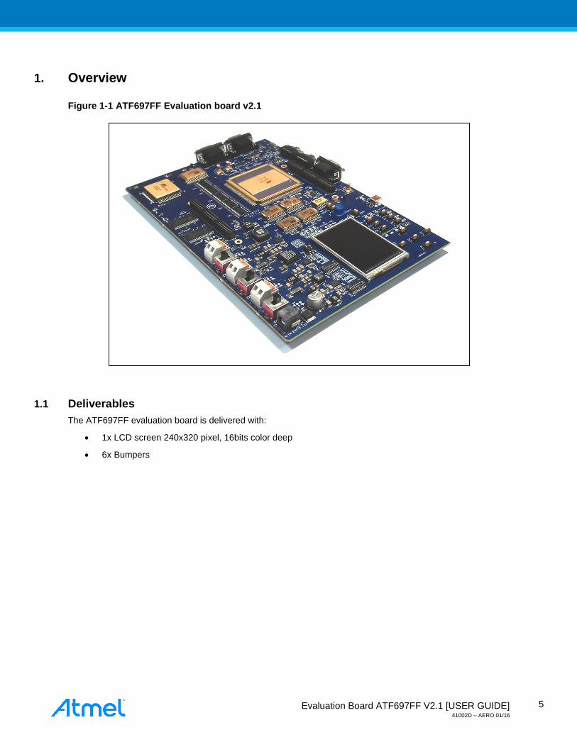
1. Overview
Figure 1-1 ATF697FF Evaluation board v2.1
1.1 Deliverables
The ATF697FF evaluation board is delivered with:
1x LCD screen 240x320 pixel, 16bits color deep
6x Bumpers
Evaluation Board ATF697FF V2.1 [USER GUIDE] 41002D – AERO 01/16
6
1.2 Features
Here is an overview of the main operational features embedded on the evaluation board:
Table 1-1. ATF697FF V2.1 board features
Characteristics Specifications
Reconfigurable processor ATF697FF, powered in 3.3V and 1.8V.
Board Power Supply
Audio jack connector (3.5mm).
3x Terminal blocks (direct 5V, 3.3V and 1.8V).
3x Power supply selector source (internal regulators or external).
Clocks generator Fixed 20 MHz, 25MHz, 33MHz, 50MHz clocks.
1x adjustable clock.
Connectors
1x SUBD9 for RS232 UART.
1x SUBD9 for RS232 Debug Interface.
1x SUBD9 for 2 CAN.
2x mini SUBD 9 for Space Wire connection.
1x USB mini B for Space programmer connection.
2x SMB for external clock input.
2x 180 pins for Mezzanine expansion connector.
1x SMB Analog input
Memories
8 Mbits flash / 32-bits wide (40-bits capability)
8 Mbits flash / 8-bits wide
16 Mbits SRAM / 32-bits wide (40-bits capability)
256 Mbits SDRAM / 32-bits wide (40-bits capability)
4x 1 Mbits EEPROM (AT17LV010)
1x 4 Mbits EEPROM (AT69170E)
User Interface
5x user interface push buttons
4x user interface LEDs
1x LCD display
1x Potentiometer
1x Temperature sensor
2x Voltage measurement
2x Current measurement
Evaluation Kit
management
1x DSU break button
1x DSU LED activity
1x Board reset press button
1x Reconfigurable Unit reset press button
1x Processor reset press button
1x Reconfigurable Unit application reset press button
1x Board reset LED
1x Reconfigurable Unit reset LED
1x Processor reset LED
1x Reconfigurable Unit OTS press button
1x Reconfigurable Unit CHECKn press button
3x LEDs for ATF697FF board activity (run, boot, error).
Evaluation Board ATF697FF V2.1 [USER GUIDE] 41002D – AERO 01/16
7
2. Hardware description
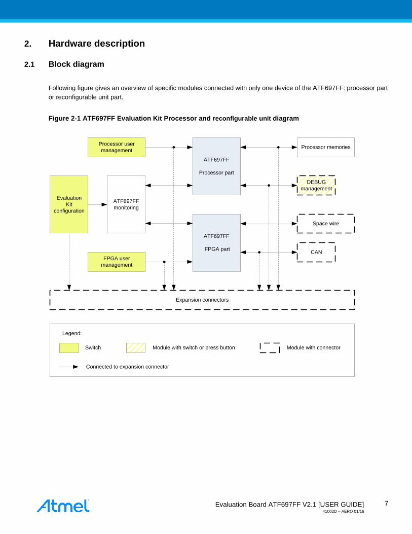
2.1 Block diagram
Following figure gives an overview of specific modules connected with only one device of the ATF697FF: processor part
or reconfigurable unit part.
Figure 2-1 ATF697FF Evaluation Kit Processor and reconfigurable unit diagram
ATF697FF
Processor part
Processor memories
DEBUG
management
FPGA user
management
ATF697FF
FPGA part
Space wire
CAN
Processor user
management
Expansion connectors
Evaluation
Kit
configuration
ATF697FF
monitoring
Legend:
Switch Module with connectorModule with switch or press button
Connected to expansion connector

Evaluation Board ATF697FF V2.1 [USER GUIDE] 41002D – AERO 01/16
8
Some evaluation kit features are connected to both processor and reconfigurable unit parts. Following diagram shows
how these modules are arranged together.
Figure 2-2 ATF697FF Evaluation Kit common parts diagram
Clock management
Reset management
Space progammer
Serial EEPROM
managementATF697FF
monitoring
status
User interface
Power management
Expansion connectors
ATF697FF
Common
part
UART
Analog sensors
SPI
I²C
Legend:
Switch
Module with connector
Module with switch or press button
Evaluation Kit configuration
Connected to expansion connector
Evaluation Board ATF697FF V2.1 [USER GUIDE] 41002D – AERO 01/16
9
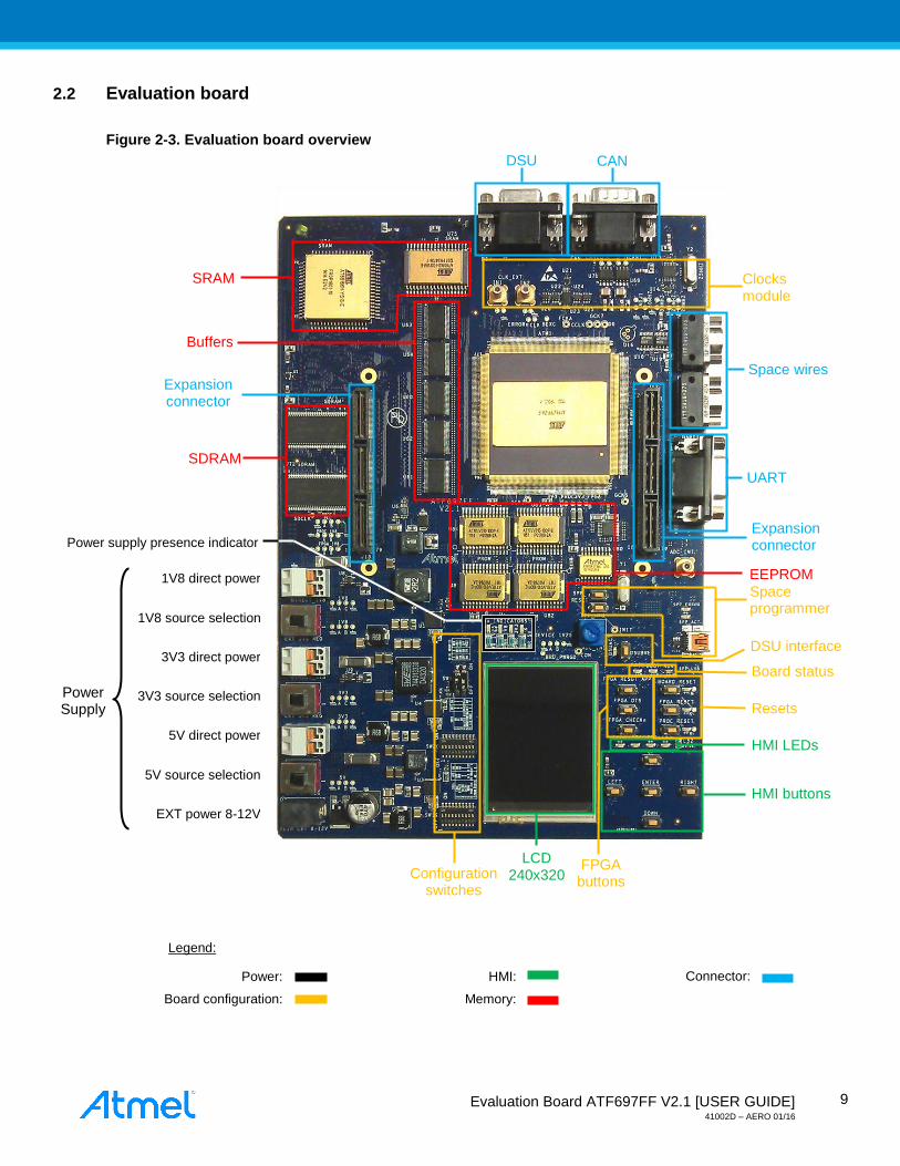
2.2 Evaluation board
Figure 2-3. Evaluation board overview
1V8 direct power
3V3 direct power
5V direct power
EXT power 8-12V
1V8 source selection
3V3 source selection
5V source selection
Power Supply
Expansion connector
Expansion connector
Buffers
HMI LEDs
HMI buttons
LCD 240x320
Resets
Board status
FPGA buttons
DSU interface
Space programmer
DSU CAN
Space wires
SRAM
SDRAM
EEPROM
Clocks module
Configuration switches
Legend:
Power:
Board configuration:
HMI:
Memory:
Connector:
UART
Power supply presence indicator

Evaluation Board ATF697FF V2.1 [USER GUIDE] 41002D – AERO 01/16
10
2.3 Manufacturing configuration
The Evaluation kit embeds several DIP switches allowing the user to configure different parameters. During this
application note, the switch is named SW and the switch number of the device is named with a “.x”. The following tables
describe the initial configurations.
Table 2-1 SW19 Default configuration switches
Name Initial state Function
SW19.1 OFF Disable EDAC
SW19.2 ON Active the Bypass (thus disable the PLL)
SW19.3 OFF SKEW 0 configuration
SW19.4 OFF SKEW 1 configuration
SW19.5 OFF Disconnect the processor watchdog to the processor reset
SW19.6 OFF Select internal 25 MHz clock as processor clock
SW19.7 OFF PROM 40 is selected
SW19.8 OFF N.C.
SW19.9 OFF N.C.
SW19.10 OFF N.C.
Table 2-2 SW20 Default configuration switches
Name Initial state Function
SW20.1 OFF M0
SW20.2 OFF M1
SW20.3 OFF M2
SW20.4 OFF Configure the processor as the master and reconfigurable unit as the slave
SW20.5 OFF Disable monitoring
SW20.6 OFF LCD display use serial connection
SW20.7 OFF N.C.
SW20.8 OFF N.C.
SW20.9 OFF N.C.
SW20.10 OFF N.C.
Evaluation Board ATF697FF V2.1 [USER GUIDE] 41002D – AERO 01/16
11
Table 2-3 SW8 Default configuration switches
Name Initial state Function
SW8.1 OFF AT17 are selected as reconfigurable unit serial memories.
SW8.2 OFF
Table 2-4 Power supply configuration switches
Name Initial state Function
SW2 REG
Internal 5V, 3.3V and 1.8V are selected as power supplies sources SW3 REG
SW4 REG
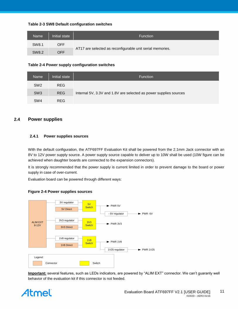
2.4 Power supplies
2.4.1 Power supplies sources
With the default configuration, the ATF697FF Evaluation Kit shall be powered from the 2.1mm Jack connector with an
8V to 12V power supply source. A power supply source capable to deliver up to 10W shall be used (10W figure can be
achieved when daughter boards are connected to the expansion connectors).
It is strongly recommended that the power supply is current limited in order to prevent damage to the board or power
supply in case of over-current.
Evaluation board can be powered through different ways:
Figure 2-4 Power supplies sources
Legend:
Connector Switch
ALIM EXT
8-12V
5V regulator5V
Switch5V Direct
PWR 5V
- 5V regulator PWR -5V
3V3 regulator3V3
Switch3V3 Direct
PWR 3V3
1V8 regulator1V8
Switch1V8 Direct
PWR 1V8
1V25 regulator PWR 1V25
Important: several features, such as LEDs indicators, are powered by “ALIM EXT” connector. We can’t guaranty well
behavior of the evaluation kit if this connector is not feeded.
Evaluation Board ATF697FF V2.1 [USER GUIDE] 41002D – AERO 01/16
12
2.4.2 Power supplies current measurement
The ATF697FF Evaluation Board offers the possibility to have an overview of the power consumption of components.
Current measurement test points are arranged according to the following drawing:
Each time the current is measured, the power line name change as shows the following figure:
Figure 2-6 Power supplies measurement
PWR 5V
PWR 1V25
PWR 3V3
DEVICE 3V3
BOARD 5V
REFERENCE 1V25
BOARD 3V3
VCC 3V3 PROC
VCC 3V3 FPGA
PWR 1V8
DEVICE 1V8
BOARD 1V8
VDD 1V8 PROC CORE
VDD 1V8 PROC PLL
VDD 1V8 FPGA CORE
Img ICC 3V3
Img ICC 1V8
Legend:
0.01R shunt resistor Differential amplifier
Voltages from amplifier are sampled by a 12 bits ADC (see analog sensor section 2.11).
2.54mm 2.54mm 2.54mm
GND GND
R shunt 0.01R
A B, C
Figure 2-5 Current probe footprint
Evaluation Board ATF697FF V2.1 [USER GUIDE] 41002D – AERO 01/16
13
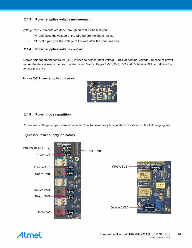
2.4.3 Power supplies voltage measurement
Voltage measurements are done through current probe test pad:
- “A” pad gives the voltage of the wire before the shunt resistor.
- “B” or “C” pad give the voltage of the wire after the shunt resistor.
2.4.4 Power supplies voltage control
A power management controller (U10) is used to detect under voltage (-10% of nominal voltage). In case of power
failure, the device keeps the board under reset. Main voltages 1V25, 1V8, 3V3 and 5V have a DEL to indicate the
voltage presence.
Figure 2-7 Power supply indicators
2.4.5 Power probe repartition
Current and voltage test pads are accessible close to power supply regulations as shown in the following figures:
Figure 2-8 Power supply indicators
PROC 1V8 Processor pll (1,8V)
FPGA 1V8
Device 1V8
Board 1V8
Device 3V3
Board 3V3
Board 5V
FPGA 3V3
Device 1V25
Evaluation Board ATF697FF V2.1 [USER GUIDE] 41002D – AERO 01/16
14
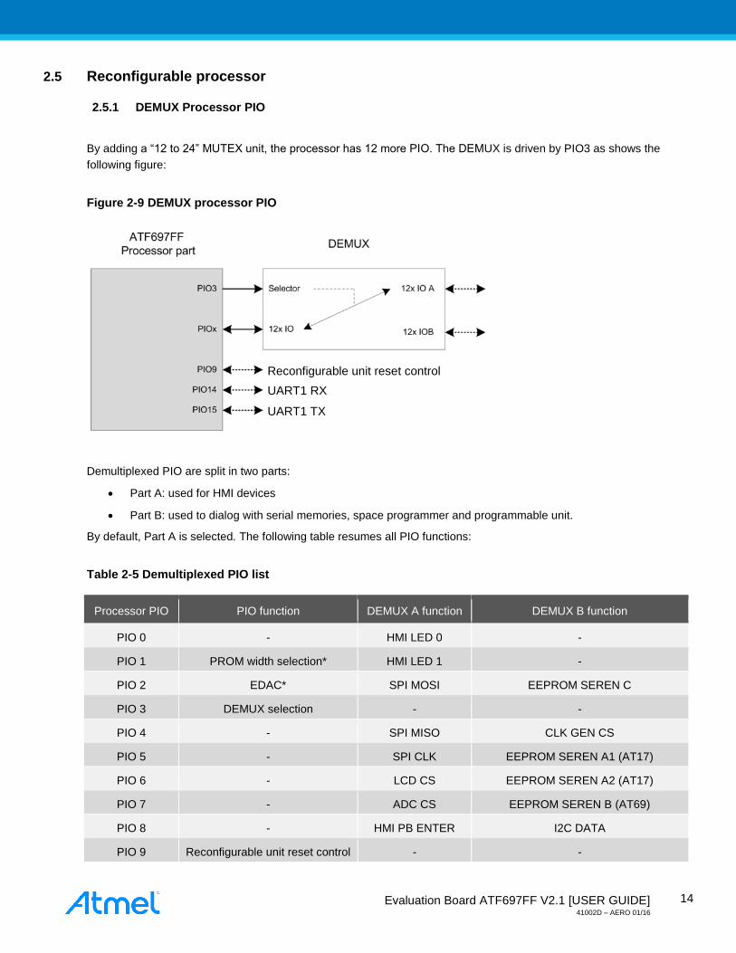
2.5 Reconfigurable processor
2.5.1 DEMUX Processor PIO
By adding a “12 to 24” MUTEX unit, the processor has 12 more PIO. The DEMUX is driven by PIO3 as shows the
following figure:
Figure 2-9 DEMUX processor PIO
Demultiplexed PIO are split in two parts:
Part A: used for HMI devices
Part B: used to dialog with serial memories, space programmer and programmable unit.
By default, Part A is selected. The following table resumes all PIO functions:
Table 2-5 Demultiplexed PIO list
Processor PIO PIO function DEMUX A function DEMUX B function
PIO 0 - HMI LED 0 -
PIO 1 PROM width selection* HMI LED 1 -
PIO 2 EDAC* SPI MOSI EEPROM SEREN C
PIO 3 DEMUX selection - -
PIO 4 - SPI MISO CLK GEN CS
PIO 5 - SPI CLK EEPROM SEREN A1 (AT17)
PIO 6 - LCD CS EEPROM SEREN A2 (AT17)
PIO 7 - ADC CS EEPROM SEREN B (AT69)
PIO 8 - HMI PB ENTER I2C DATA
PIO 9 Reconfigurable unit reset control - -
Reconfigurable unit reset control
UART1 RX
UART1 TX
Evaluation Board ATF697FF V2.1 [USER GUIDE] 41002D – AERO 01/16
15
Processor PIO PIO function DEMUX A function DEMUX B function
PIO10 - HMI PB DOWN I2C SCL
PIO11 - HMI PB UP INIT
PIO 12 - HMI PB RIGHT CS0n
PIO 13 - HMI PB LEFT CON
PIO 14 UART1 RX - -
PIO 15 UART1 TX - -
Note *: these functions are only used during processor start sequence to parameter some registers.
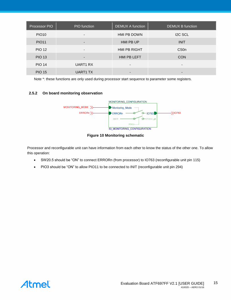
2.5.2 On board monitoring observation
Figure 10 Monitoring schematic
Processor and reconfigurable unit can have information from each other to know the status of the other one. To allow
this operation:
SW20.5 should be “ON” to connect ERRORn (from processor) to IO763 (reconfigurable unit pin 115)
PIO3 should be “ON” to allow PIO11 to be connected to INIT (reconfigurable unit pin 294)
Evaluation Board ATF697FF V2.1 [USER GUIDE] 41002D – AERO 01/16
16
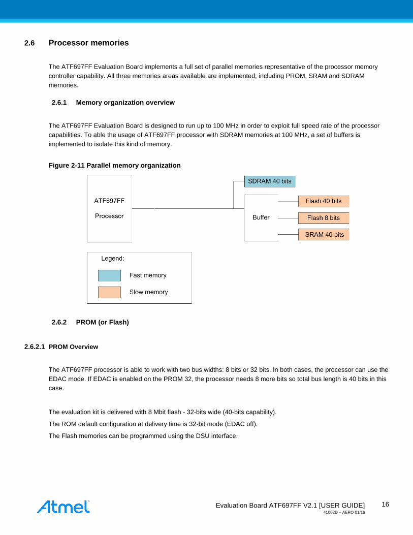
2.6 Processor memories
The ATF697FF Evaluation Board implements a full set of parallel memories representative of the processor memory
controller capability. All three memories areas available are implemented, including PROM, SRAM and SDRAM
memories.
2.6.1 Memory organization overview
The ATF697FF Evaluation Board is designed to run up to 100 MHz in order to exploit full speed rate of the processor
capabilities. To able the usage of ATF697FF processor with SDRAM memories at 100 MHz, a set of buffers is
implemented to isolate this kind of memory.
Figure 2-11 Parallel memory organization
2.6.2 PROM (or Flash)
2.6.2.1 PROM Overview
The ATF697FF processor is able to work with two bus widths: 8 bits or 32 bits. In both cases, the processor can use the
EDAC mode. If EDAC is enabled on the PROM 32, the processor needs 8 more bits so total bus length is 40 bits in this
case.
The evaluation kit is delivered with 8 Mbit flash - 32-bits wide (40-bits capability).
The ROM default configuration at delivery time is 32-bit mode (EDAC off).
The Flash memories can be programmed using the DSU interface.
Evaluation Board ATF697FF V2.1 [USER GUIDE] 41002D – AERO 01/16
17
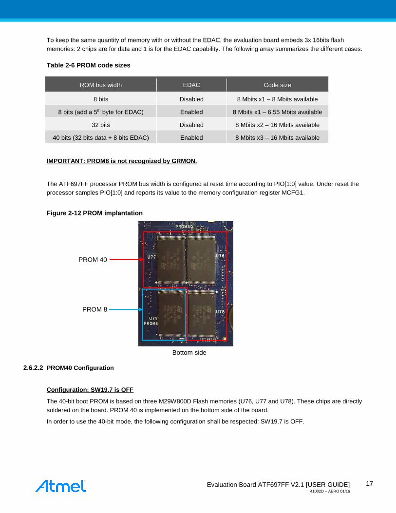
To keep the same quantity of memory with or without the EDAC, the evaluation board embeds 3x 16bits flash
memories: 2 chips are for data and 1 is for the EDAC capability. The following array summarizes the different cases.
Table 2-6 PROM code sizes
ROM bus width EDAC Code size
8 bits Disabled 8 Mbits x1 – 8 Mbits available
8 bits (add a 5th byte for EDAC) Enabled 8 Mbits x1 – 6.55 Mbits available
32 bits Disabled 8 Mbits x2 – 16 Mbits available
40 bits (32 bits data + 8 bits EDAC) Enabled 8 Mbits x3 – 16 Mbits available
IMPORTANT: PROM8 is not recognized by GRMON.
The ATF697FF processor PROM bus width is configured at reset time according to PIO[1:0] value. Under reset the
processor samples PIO[1:0] and reports its value to the memory configuration register MCFG1.
Figure 2-12 PROM implantation
2.6.2.2 PROM40 Configuration
Configuration: SW19.7 is OFF
The 40-bit boot PROM is based on three M29W800D Flash memories (U76, U77 and U78). These chips are directly
soldered on the board. PROM 40 is implemented on the bottom side of the board.
In order to use the 40-bit mode, the following configuration shall be respected: SW19.7 is OFF.
PROM 40
PROM 8
Bottom side
Evaluation Board ATF697FF V2.1 [USER GUIDE] 41002D – AERO 01/16
18
2.6.2.3 PROM8 Configuration
Configuration: SW19.7 is ON
The 8-bit boot PROM is based on onM29W800D Flash memory (U79). The chip is directly soldered on the board.
PROM8 is implemented on the bottom side of the board close to the PROM40.
IMPORTANT: when EDAC is activated with PROM8, memory available is less than without EDAC.
2.6.2.4 PROM Expansion
The ATF697FF processor can control up to 512Mbytes of PROM. The evaluation board can handle up to 16M bytes of
PROM code. For applications that need more PROM capacity, it is possible to extend the total PROM capacity by
connecting a daughter board to the expansion connectors.
All PROM control signals are provided on these expansion connectors.
Please refer to the ““Expansion Connectors - section 2.17” for details on signal assignment.
2.6.3 RAM Overview
The ATF697FF Evaluation Board allows the user to execute code in SRAM or in SDRAM.
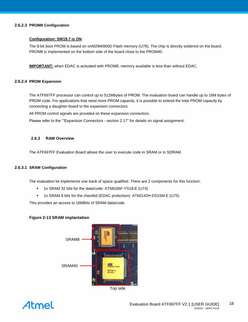
2.6.3.1 SRAM Configuration
The evaluation kit implements one bank of space qualified. There are 2 components for this function:
1x SRAM 32 bits for the data/code: AT68166F-YS18-E (U74)
1x SRAM 8 bits for the checkbit (EDAC protection): AT60142H-DS15M-E (U75)
This provides an access to 16MBits of SRAM data/code.
Figure 2-13 SRAM implantation
Top side
SRAM8
SRAM40
Evaluation Board ATF697FF V2.1 [USER GUIDE] 41002D – AERO 01/16
19
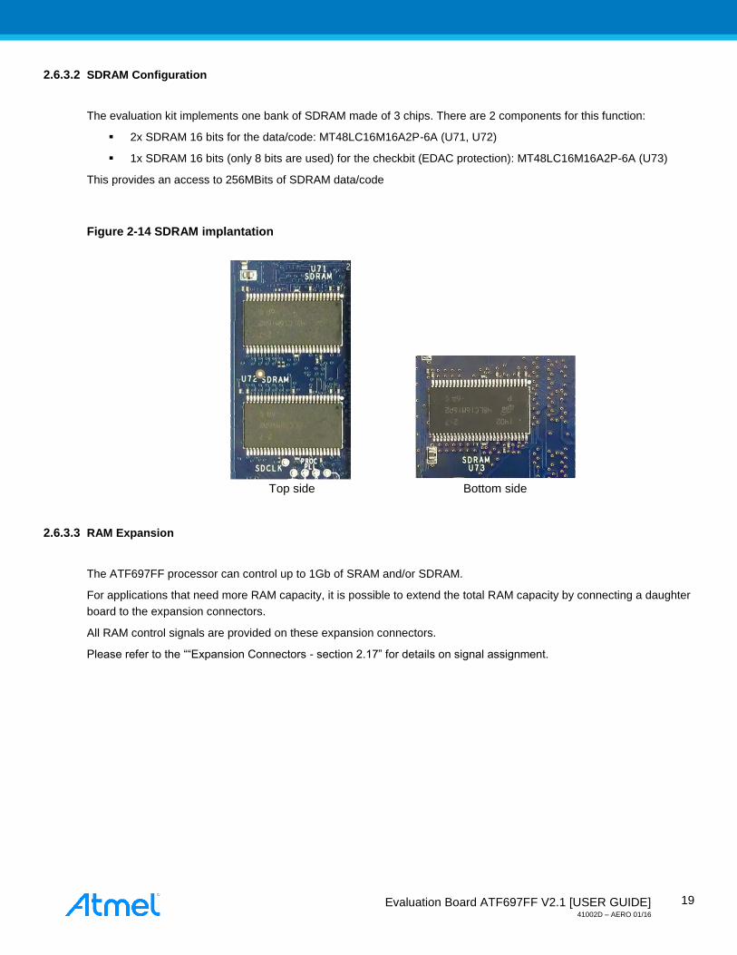
2.6.3.2 SDRAM Configuration
The evaluation kit implements one bank of SDRAM made of 3 chips. There are 2 components for this function:
2x SDRAM 16 bits for the data/code: MT48LC16M16A2P-6A (U71, U72)
1x SDRAM 16 bits (only 8 bits are used) for the checkbit (EDAC protection): MT48LC16M16A2P-6A (U73)
This provides an access to 256MBits of SDRAM data/code
Figure 2-14 SDRAM implantation
2.6.3.3 RAM Expansion
The ATF697FF processor can control up to 1Gb of SRAM and/or SDRAM.
For applications that need more RAM capacity, it is possible to extend the total RAM capacity by connecting a daughter
board to the expansion connectors.
All RAM control signals are provided on these expansion connectors.
Please refer to the ““Expansion Connectors - section 2.17” for details on signal assignment.
Top side Bottom side
Evaluation Board ATF697FF V2.1 [USER GUIDE] 41002D – AERO 01/16
20
2.7 Reconfigurable unit memories
2.7.1 Reconfigurable unit configuration mode
During the boot sequence, the reconfigurable units can be configured as master or as slave to drive the clock during the
downloading of the bitstream. Followings switches allow to change this configuration:
Table 2-7 reconfigurable unit configuration mode switches
Switch number Function
SW20.1 Configure M0
SW20.2 Configure M1
SW20.3 Configure M2
2.7.2 Memory organization overview
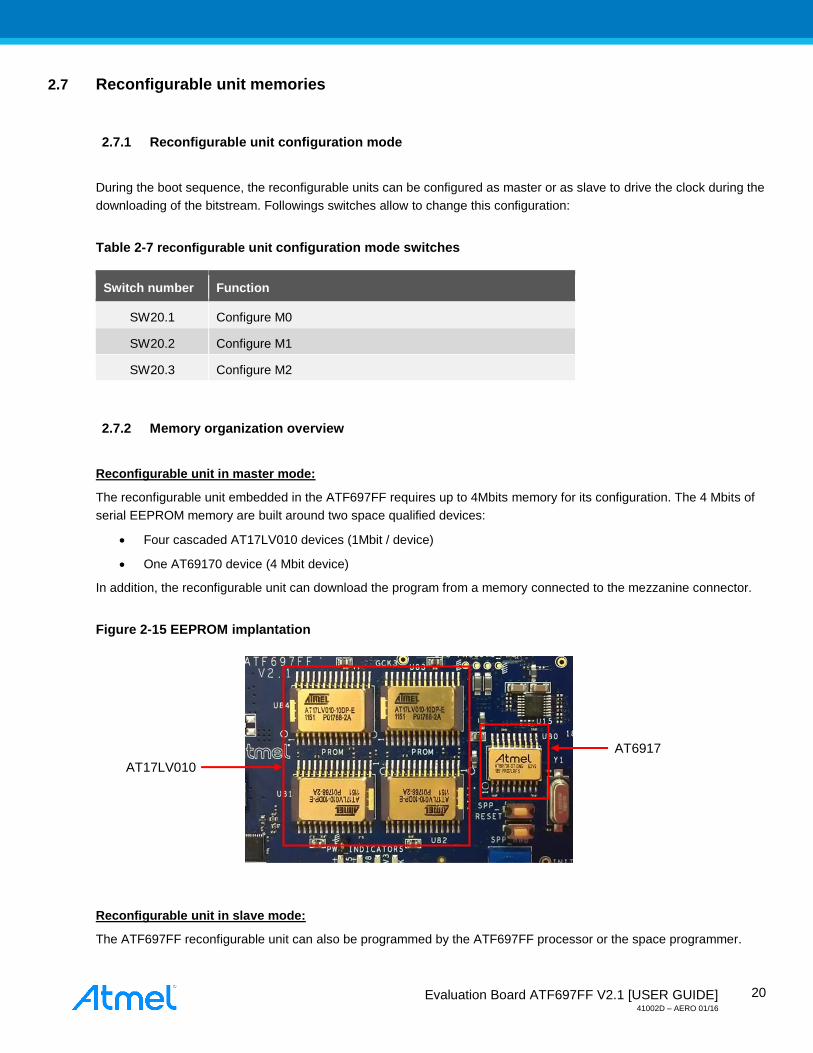
Reconfigurable unit in master mode:
The reconfigurable unit embedded in the ATF697FF requires up to 4Mbits memory for its configuration. The 4 Mbits of
serial EEPROM memory are built around two space qualified devices:
Four cascaded AT17LV010 devices (1Mbit / device)
One AT69170 device (4 Mbit device)
In addition, the reconfigurable unit can download the program from a memory connected to the mezzanine connector.
Figure 2-15 EEPROM implantation
Reconfigurable unit in slave mode:
The ATF697FF reconfigurable unit can also be programmed by the ATF697FF processor or the space programmer.
AT17LV010
AT6917
Evaluation Board ATF697FF V2.1 [USER GUIDE] 41002D – AERO 01/16
21
Figure 2-16 Serial memory organization
ATF697FF
FPGA part
Legend:
ATF697FF
AT69
AT17
AT17
AT17
AT17
Logic
Mezzanine
ATF697FF
Processor
Space programmer
I²CIO713_D0
CCLK
FPGA_RESETnReset
module
EEPROM READY
CTRL 1
CTRL 4
CTRL 0
CTRL 8
CTRL 3
EEPROM SEREN A1
EEPROM SEREN B
EEPROM SEREN C
IO547_CS0n
IO303_INIT
CON
EEPROM selection SW8
User interface switch
Connector
2
2
I²C
Chip select
EEPROM ready
DEMUX
PIO
EEPROM SEREN A2
PIO 12 B
PIO 2 B
PIO 7 B
PIO 6 B
PIO 5 B
Evaluation Board ATF697FF V2.1 [USER GUIDE] 41002D – AERO 01/16
22
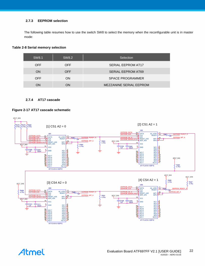
2.7.3 EEPROM selection
The following table resumes how to use the switch SW8 to select the memory when the reconfigurable unit is in master
mode:
Table 2-8 Serial memory selection
SW8.1 SW8.2 Selection
OFF OFF SERIAL EEPROM AT17
ON OFF SERIAL EEPROM AT69
OFF ON SPACE PROGRAMMER
ON ON MEZZANINE SERIAL EEPROM
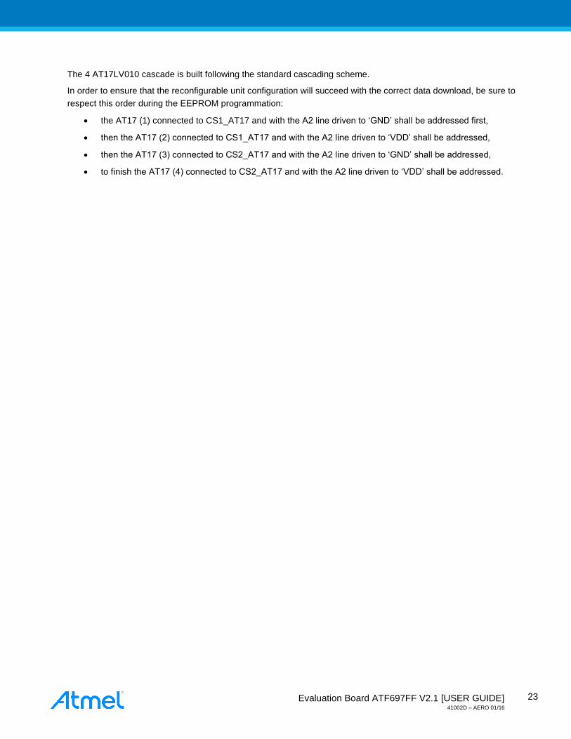
2.7.4 AT17 cascade
Figure 2-17 AT17 cascade schematic
[1] CS1 A2 = 0 [2] CS1 A2 = 1
[3] CS4 A2 = 0 [4] CS4 A2 = 1
Evaluation Board ATF697FF V2.1 [USER GUIDE] 41002D – AERO 01/16
23
The 4 AT17LV010 cascade is built following the standard cascading scheme.
In order to ensure that the reconfigurable unit configuration will succeed with the correct data download, be sure to
respect this order during the EEPROM programmation:
the AT17 (1) connected to CS1_AT17 and with the A2 line driven to ‘GND’ shall be addressed first,
then the AT17 (2) connected to CS1_AT17 and with the A2 line driven to ‘VDD’ shall be addressed,
then the AT17 (3) connected to CS2_AT17 and with the A2 line driven to ‘GND’ shall be addressed,
to finish the AT17 (4) connected to CS2_AT17 and with the A2 line driven to ‘VDD’ shall be addressed.
Evaluation Board ATF697FF V2.1 [USER GUIDE] 41002D – AERO 01/16
24
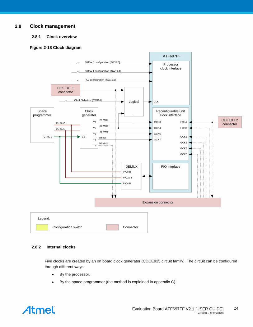
2.8 Clock management
2.8.1 Clock overview
Figure 2-18 Clock diagram
Clock
generator
AT697F
Logical
CLK EXT 1
connector
Legend:
Configuration switch Connector
Processor
clock interface
PIO interface
Reconfigurable unit
clock interface
CLK
GCK320 MHz
25 MHzGCK4
33 MHzGCK5
50 MHz
GCK7
CLK EXT 2
connector
GCK2
GCK1
GCK6
GCK8
Space
programmer
I2C SCL
I2C SDA
CSCTRL 2
DEMUX
PIO8 B
PIO10 B
PIO4 B
adjust
FCKA
FCKB
Expansion connector
Y1
Y2
Y3
Y4
Y5
PLL configuration [SW19.2]
SKEW 1 configuration [SW19.4]
SKEW 0 configuration [SW19.3]
Clock Selection [SW19.6]
2.8.2 Internal clocks
Five clocks are created by an on board clock generator (CDCE925 circuit family). The circuit can be configured
through different ways:
By the processor.
By the space programmer (the method is explained in appendix C).
ATF697FF

Evaluation Board ATF697FF V2.1 [USER GUIDE] 41002D – AERO 01/16
25
The default configuration of the CDCE925 is:
Table 2-9 CDCE925 default configuration
Circuit clock out Frequency
Y1 20 MHz
Y2 25 MHz
Y3 33 MHz
Y4 50 MHz
Y5 10 MHz (adjustable clock)
2.8.3 External clocks
Two SMB male connectors are accessible from the front panel of the Evaluation Kit:
Clock EXT IN 1: alternate processor clock, used if SW19.6 = ON.
Clock EXT IN 2: connected to expansion connectors.
2.8.4 Processor clock configuration
Configuration switches SW19 allow the user to manage processor clock configuration.
Table 2-10 Clock configuration
Name Switch number Function Pin number
BYPASS SW19.2 OFF: PLL enable, master clock frequency is 4x CLK frequencies.
ON: PLL disabled, master clock frequency is CLK frequency.
143
SKEW 0 SW19.3 OFF: SKEW0 disabled
ON: SKEW0 enable
136
SKEW 1 SW19.4 OFF: SKEW1 disabled
ON: SKEW1 enable
137
CLK SW19.6 OFF: processor use on-board 25MHz clock
ON: processor use Clock EXT IN 1
144
Evaluation Board ATF697FF V2.1 [USER GUIDE] 41002D – AERO 01/16
26
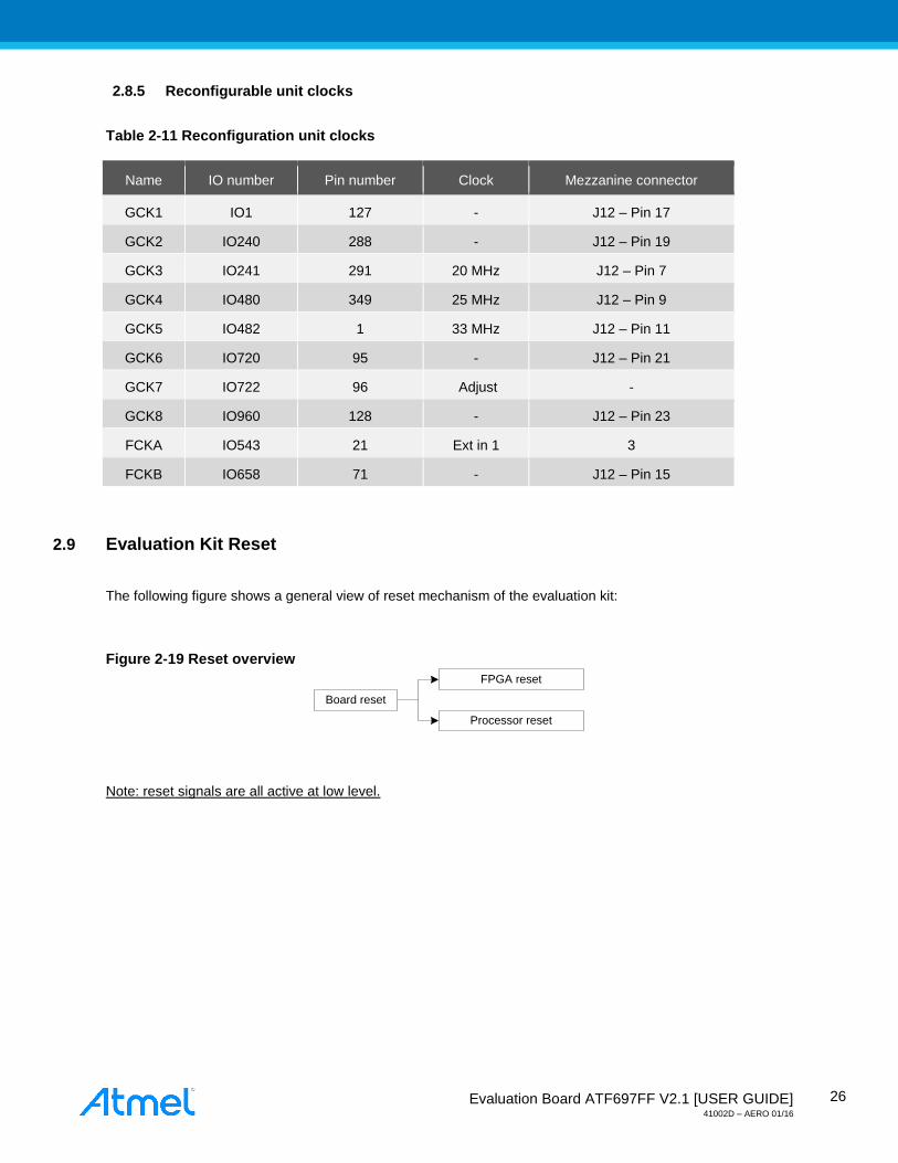
2.8.5 Reconfigurable unit clocks
Table 2-11 Reconfiguration unit clocks
Name IO number Pin number Clock Mezzanine connector
GCK1 IO1 127 - J12 – Pin 17
GCK2 IO240 288 - J12 – Pin 19
GCK3 IO241 291 20 MHz J12 – Pin 7
GCK4 IO480 349 25 MHz J12 – Pin 9
GCK5 IO482 1 33 MHz J12 – Pin 11
GCK6 IO720 95 - J12 – Pin 21
GCK7 IO722 96 Adjust -
GCK8 IO960 128 - J12 – Pin 23
FCKA IO543 21 Ext in 1 3
FCKB IO658 71 - J12 – Pin 15
2.9 Evaluation Kit Reset
The following figure shows a general view of reset mechanism of the evaluation kit:
Figure 2-19 Reset overview
Board reset
FPGA reset
Processor reset
Note: reset signals are all active at low level.
Evaluation Board ATF697FF V2.1 [USER GUIDE] 41002D – AERO 01/16
27
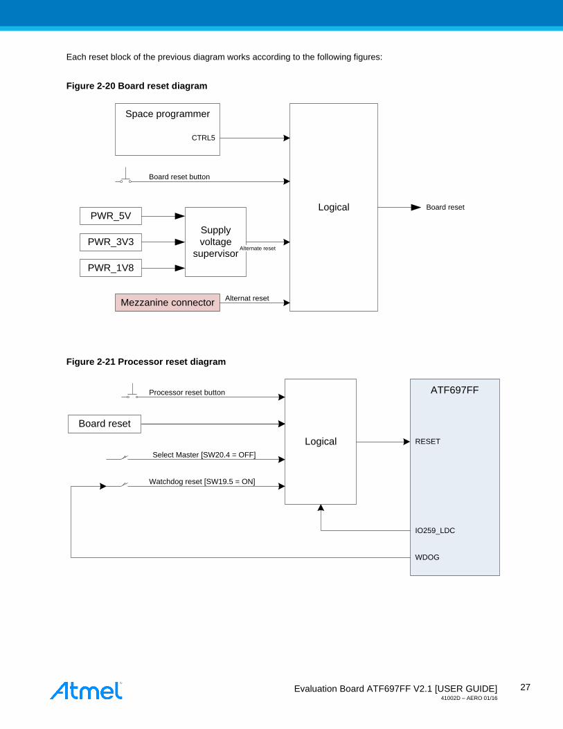
Each reset block of the previous diagram works according to the following figures:
Figure 2-20 Board reset diagram
PWR_5V
PWR_3V3
PWR_1V8
Supply
voltage
supervisor
Logical
Space programmer
Mezzanine connectorAlternat reset
CTRL5
Board reset
Board reset button
Figure 2-21 Processor reset diagram
ATF697FF
RESET
WDOG
IO259_LDC
Select Master [SW20.4 = OFF]
Logical
Board reset
Watchdog reset [SW19.5 = ON]
Processor reset button
Alternate reset

Evaluation Board ATF697FF V2.1 [USER GUIDE] 41002D – AERO 01/16
28
Figure 2-22 Reconfigurable unit reset diagram
ATF697FF
Mezzanine connector
FPGA RESET
PIO9
Logical
AT17 (x4)
AT69
EEPROM READY
Select Master [SW20.4 = ON]
FPGA reset button
Board reset
2.9.1 Alternate reset
An alternate reset is available on the expansion connector. Please refer to the “Expansion Connectors - section 2.17”
for detailed information on expansion connector assignments.
2.9.2 Supply voltage supervisor
An integrated circuit measures PWR_5V, PWR_3V3 and PWR_1V8 signals on the board. If these voltages are out of
range (+/- 10% nominal value), the circuit reset the board or keep the board under reset (during a power on for
example).
2.9.3 Space Programmer (SPP) reset
It is possible to reset the Eveluation Board by driving low CTRL_GEN5 of the SPP connector.
2.9.4 Watchdog reset
By using SW37.5, it’s possible to connect processor Watchdog pin WDOG (pin 148) to the processor reset module.
Table 2-12 Watchdog configuration
Name Switch number Function Processor pin
Watchdog SW19.5 OFF: disconnect WDOG pin to reset module
ON: connect WDOG pin to reset module 148
Evaluation Board ATF697FF V2.1 [USER GUIDE] 41002D – AERO 01/16
29
2.9.5 Self resets
Processor can reset the reconfigurable unit part as well the reconfigurable unit can reset the processor. The following
table shows how to configure switch SW20 of the board to select the master:
Table 2-13 Master reset configuration
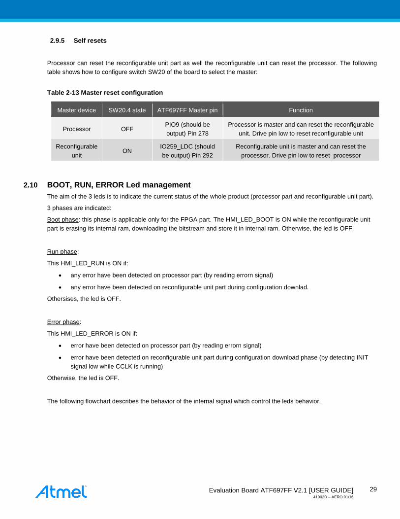
2.10 BOOT, RUN, ERROR Led management
The aim of the 3 leds is to indicate the current status of the whole product (processor part and reconfigurable unit part).
3 phases are indicated:
Boot phase: this phase is applicable only for the FPGA part. The HMI_LED_BOOT is ON while the reconfigurable unit
part is erasing its internal ram, downloading the bitstream and store it in internal ram. Otherwise, the led is OFF.
Run phase:
This HMI_LED_RUN is ON if:
any error have been detected on processor part (by reading errorn signal)
any error have been detected on reconfigurable unit part during configuration downlad.
Othersises, the led is OFF.
Error phase:
This HMI_LED_ERROR is ON if:
error have been detected on processor part (by reading errorn signal)
error have been detected on reconfigurable unit part during configuration download phase (by detecting INIT
signal low while CCLK is running)
Otherwise, the led is OFF.
The following flowchart describes the behavior of the internal signal which control the leds behavior.
Master device SW20.4 state ATF697FF Master pin Function
Processor OFF PIO9 (should be
output) Pin 278
Processor is master and can reset the reconfigurable
unit. Drive pin low to reset reconfigurable unit
Reconfigurable
unit ON
IO259_LDC (should
be output) Pin 292
Reconfigurable unit is master and can reset the
processor. Drive pin low to reset processor
Evaluation Board ATF697FF V2.1 [USER GUIDE] 41002D – AERO 01/16
30
Figure 2-23 BOOT_FPGA, RUN_FPGA, ERROR_FPGA, BOOT_PROC, RUN_PROC, ERROR_PROC signals flowcharts
0
0
0
Fpga_resetn_’0'
Fpga_resetn_’1'
1
CON rising edge
while CCLK is running
RUN_FPGA
1
1
1
Fpga_resetn_’0'
Fpga_resetn_’1'
0
CON rising edge
while CCLK is running
BOOT_FPGA
0
1
0
Fpga_resetn_’0'
Fpga_resetn_’1'
0
INIT=0
& CON=0
& CCLK is running
ERROR_FPGA
1
INIT=1
& CON=0
& CCLK is running
BOOT_PROC
NA
ERROR_PROC
0
1
Errorn=’0'
RUN_PROC
1
0
Errorn=’0'
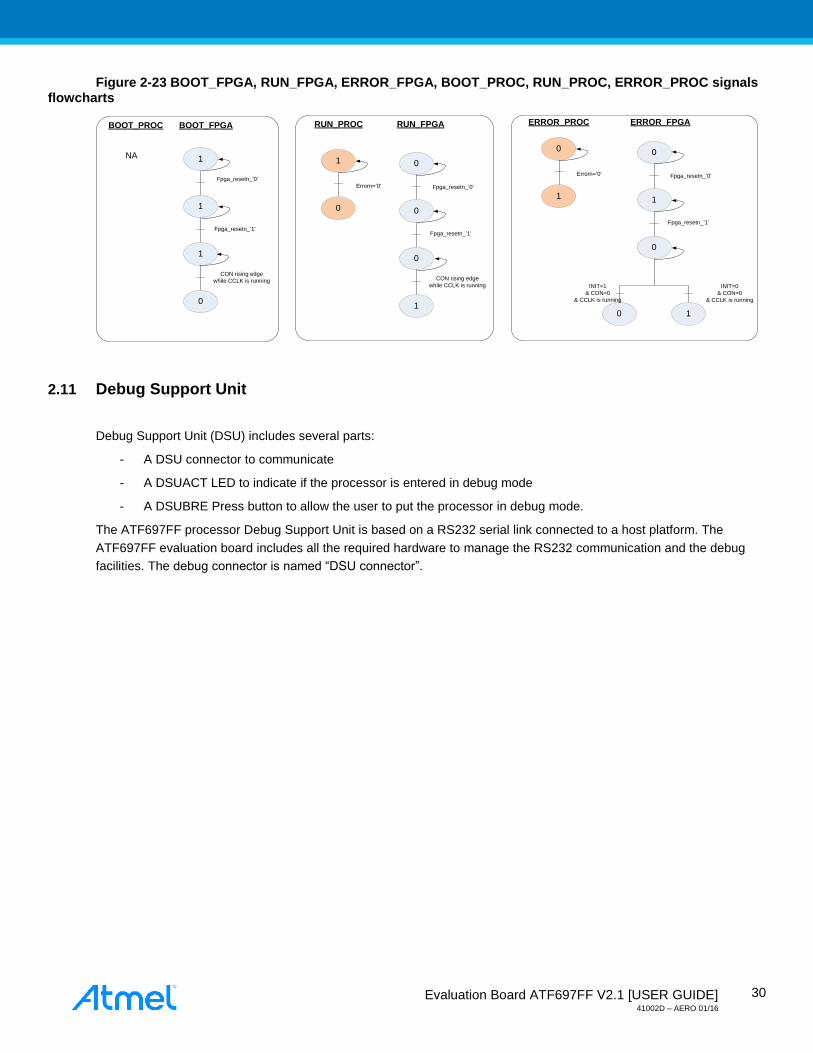
2.11 Debug Support Unit
Debug Support Unit (DSU) includes several parts:
- A DSU connector to communicate
- A DSUACT LED to indicate if the processor is entered in debug mode
- A DSUBRE Press button to allow the user to put the processor in debug mode.
The ATF697FF processor Debug Support Unit is based on a RS232 serial link connected to a host platform. The
ATF697FF evaluation board includes all the required hardware to manage the RS232 communication and the debug
facilities. The debug connector is named “DSU connector”.
Evaluation Board ATF697FF V2.1 [USER GUIDE] 41002D – AERO 01/16
31
Figure 2-24 DSU implementation
2.12 Multi channels ADC
The ATF697FF evaluation board embeds 8 channels 12bits Analogue to Digital Converter from Analogue Devices: the
AD7888. The device is connected to the processor and the reconfigurable unit through SPI connection as shows le
following table:
Table 2-14 ADC connection
ADC function Processor connection reconfigurable unit AFT697FF pin
SPI MISO PIO4_A IO407 320
SPI MOSI PIO2_A IO403 318
SPI CLK PIO5_A IO411 323
SPI CS PIO7_A IO425 328
The ADC has 8 channels connected to different probes of the evaluation kit:
Table 2-15 ADC channels mapping
ADC channel Sampled signal
CH1 On board potentiometer
CH2 On board temperature sensor
DSU connector
DSU break Press button
DSUACT indicator
Evaluation Board ATF697FF V2.1 [USER GUIDE] 41002D – AERO 01/16
32
ADC channel Sampled signal
CH3 3.3V Voltage supplying ATF697FF
CH4 Consumed current by 3.3V by the ATF697FF
CH5 1.8V Voltage supplying ATF697FF
CH6 Consumed current by 1.8V by the ATF697FF
CH7 Voltage from SMB connector
CH8 N.C.
The current measurement is done through a 0.01 ohm resistor. Because the measured differential signal is very small,
an amplifier used as non inverted differential boost the signal to allow good conversion of the ADC. At start, the
reconfigurable unit may use lot of power during a short period. To protect the ADC, a Zener diode is added between the
amplifier and the converter. Equations to calculate the consumed current are:
𝑈𝐴𝑚𝑝𝑙𝑖𝑒𝑟𝐼𝑁 = 𝑅 ∗ 𝐼
𝑈𝐴𝐷𝐶𝐼𝑁 = 𝑈𝐴𝑚𝑝𝑙𝑖𝑒𝑟𝑂𝑈𝑇 = 𝑈𝐴𝑚𝑝𝑙𝑖𝑒𝑟𝐼𝑁 ∗ 𝐺
Where:
I is the current,
R the 0.01 shunt resistor
G is the gain
Only G is different between 1.8V and 3.3V current measurement:
G3.3V = 39
G1.8V = 100
Finally, we have:
𝐼3.3𝑉 = 0.39 ∗ 𝑈𝐴𝐷𝐶𝐶𝐻4
𝐼1.8𝑉 = 𝑈𝐴𝐷𝐶𝐶𝐻6
2.13 Board HMI
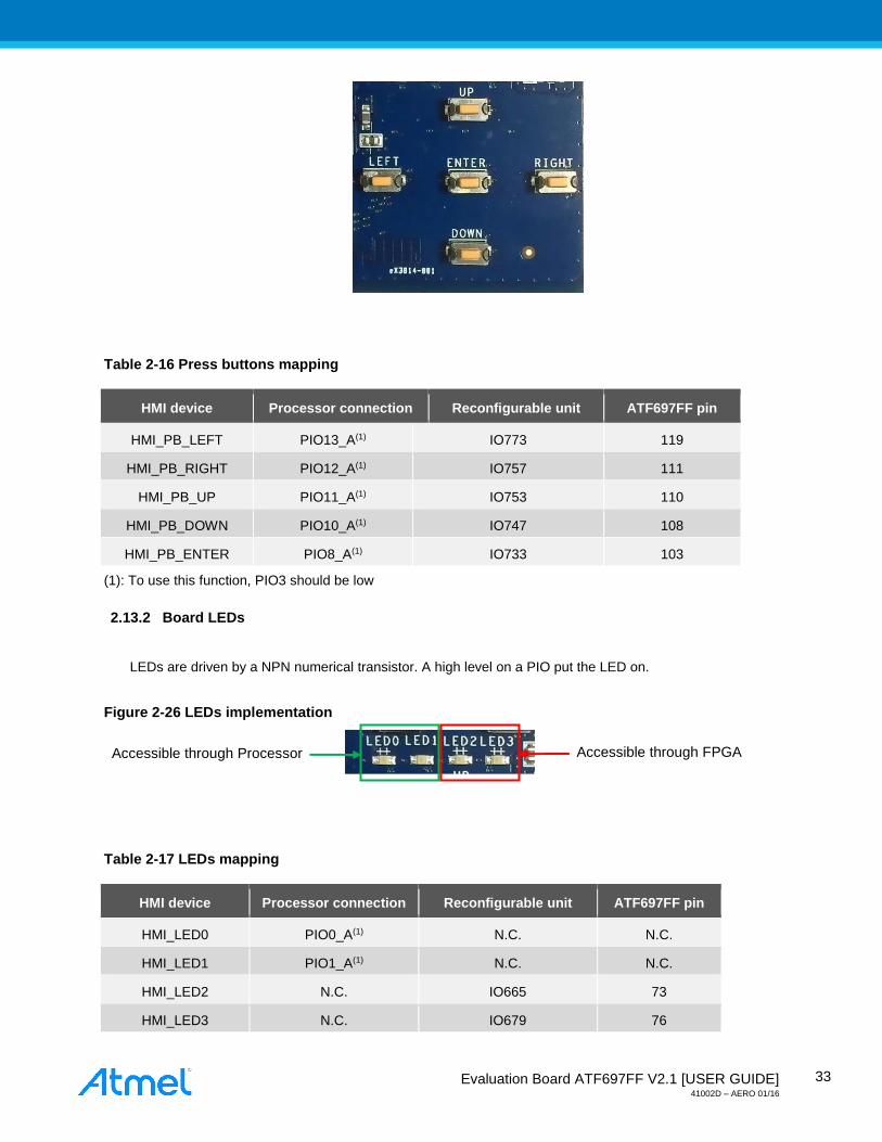
The user can interact with the board through press buttons, LEDs and an LCD display.
2.13.1 Board press buttons
Press buttons are all pulled up to 3.3V with a 4.7KΩ resistor thus when the button is pressed, the signal goes low. An
anti-bounce filter is present close to each press button to avoid wrong detection.
Figure 2-25 Press button implantation
Evaluation Board ATF697FF V2.1 [USER GUIDE] 41002D – AERO 01/16
33
Table 2-16 Press buttons mapping
HMI device Processor connection Reconfigurable unit ATF697FF pin
HMI_PB_LEFT PIO13_A(1) IO773 119
HMI_PB_RIGHT PIO12_A(1) IO757 111
HMI_PB_UP PIO11_A(1) IO753 110
HMI_PB_DOWN PIO10_A(1) IO747 108
HMI_PB_ENTER PIO8_A(1) IO733 103
(1): To use this function, PIO3 should be low
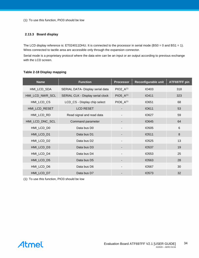
2.13.2 Board LEDs
LEDs are driven by a NPN numerical transistor. A high level on a PIO put the LED on.
Figure 2-26 LEDs implementation
Table 2-17 LEDs mapping
HMI device Processor connection Reconfigurable unit ATF697FF pin
HMI_LED0 PIO0_A(1) N.C. N.C.
HMI_LED1 PIO1_A(1) N.C. N.C.
HMI_LED2 N.C. IO665 73
HMI_LED3 N.C. IO679 76
Accessible through Processor Accessible through FPGA
Evaluation Board ATF697FF V2.1 [USER GUIDE] 41002D – AERO 01/16
34
(1): To use this function, PIO3 should be low
2.13.3 Board display
The LCD display reference is: ET024011DHU. It is connected to the processor in serial mode (BS0 = 0 and BS1 = 1).
Wires connected to tactile area are accessible only through the expansion connector.
Serial mode is a proprietary protocol where the data wire can be an input or an output according to previous exchange
with the LCD screen.
Table 2-18 Display mapping
Name Function Processor Reconfigurable unit ATF697FF pin
HMI_LCD_SDA SERIAL DATA- Display serial data PIO2_A(1) IO403 318
HMI_LCD_NWR_SCL SERIAL CLK - Display serial clock PIO5_A(1) IO411 323
HMI_LCD_CS LCD_CS - Display chip select PIO6_A(1) IO651 68
HMI_LCD_RESET LCD RESET - IO611 53
HMI_LCD_RD Read signal and read data - IO627 59
HMI_LCD_DNC_SCL Command parameter - IO645 64
HMI_LCD_D0 Data bus D0 - IO505 6
HMI_LCD_D1 Data bus D1 - IO511 8
HMI_LCD_D2 Data bus D2 - IO525 13
HMI_LCD_D3 Data bus D3 - IO537 19
HMI_LCD_D4 Data bus D4 - IO553 25
HMI_LCD_D5 Data bus D5 - IO563 28
HMI_LCD_D6 Data bus D6 - IO567 30
HMI_LCD_D7 Data bus D7 - IO573 32
(1): To use this function, PIO3 should be low
Evaluation Board ATF697FF V2.1 [USER GUIDE] 41002D – AERO 01/16
35
2.13.4 Reconfigurable units dedicated press buttons
The user can interact with specifics reconfigurable units function through press buttons:
Name Pin Function
IO225_OTSn 287 Configure all reconfigurable units I/O in Tri-State mode
IO665_CHECKn 73 To enable CHECK function when download start
IO793_APP_RESETn 126 Dedicated pin for program to do a application reset (software reset)
Figure 2-27 Reconfigurable unit button implementation
2.14 UART interface
The ATF697FF evaluation board includes all the required hardware to manage a RS232 communication. Hardware flow
control (CTS & RTS) are not implemented on this Evaluation Kit.
2.14.1 Serial link 1
Serial link 1 is available on the board through the UART 1 connector. The connector is a SUBD9 female type.
Table 2-19 UART1 ATF697FF mapping
Serial link name Function Processor connection Reconfigurable unit ATF697FF pin
UART1_RX Serial link receive data PIO 14 IO385 313
UART1_TX Serial link transmit data PIO 15 IO387 314
UART1_RTS Request to Send frame N.C. N.C. -
UART1_CTS Clear to Send frame N.C. N.C. -
Evaluation Board ATF697FF V2.1 [USER GUIDE] 41002D – AERO 01/16
36
Table 2-20 UART1 connector pinout
DB9 Pin Function
1 -
2 UART1_TX
3 UART1_RX
4 -
5 GND
6 -
7 -
8 -
9 -
2.14.2 Serial link 2
Serial link 2 is available through the expansion connector only and is only 3.3V tolerant. If serial link 2 is connected to a
RS232 interface on an expansion board, a line driver (like MAX3232) has to be implemented to adapt voltage.
Evaluation Board ATF697FF V2.1 [USER GUIDE] 41002D – AERO 01/16
37
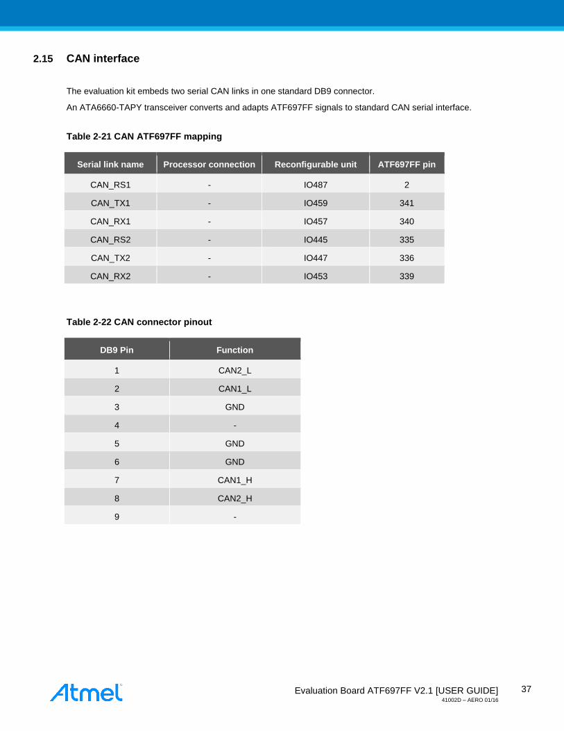
2.15 CAN interface
The evaluation kit embeds two serial CAN links in one standard DB9 connector.
An ATA6660-TAPY transceiver converts and adapts ATF697FF signals to standard CAN serial interface.
Table 2-21 CAN ATF697FF mapping
Serial link name Processor connection Reconfigurable unit ATF697FF pin
CAN_RS1 - IO487 2
CAN_TX1 - IO459 341
CAN_RX1 - IO457 340
CAN_RS2 - IO445 335
CAN_TX2 - IO447 336
CAN_RX2 - IO453 339
Table 2-22 CAN connector pinout
DB9 Pin Function
1 CAN2_L
2 CAN1_L
3 GND
4 -
5 GND
6 GND
7 CAN1_H
8 CAN2_H
9 -
Evaluation Board ATF697FF V2.1 [USER GUIDE] 41002D – AERO 01/16
38
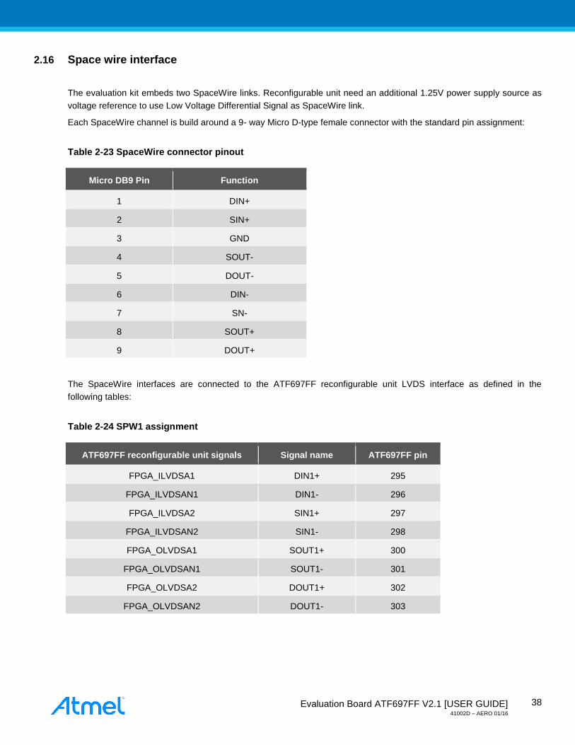
2.16 Space wire interface
The evaluation kit embeds two SpaceWire links. Reconfigurable unit need an additional 1.25V power supply source as
voltage reference to use Low Voltage Differential Signal as SpaceWire link.
Each SpaceWire channel is build around a 9- way Micro D-type female connector with the standard pin assignment:
Table 2-23 SpaceWire connector pinout
Micro DB9 Pin Function
1 DIN+
2 SIN+
3 GND
4 SOUT-
5 DOUT-
6 DIN-
7 SN-
8 SOUT+
9 DOUT+
The SpaceWire interfaces are connected to the ATF697FF reconfigurable unit LVDS interface as defined in the
following tables:
Table 2-24 SPW1 assignment
ATF697FF reconfigurable unit signals Signal name ATF697FF pin
FPGA_ILVDSA1 DIN1+ 295
FPGA_ILVDSAN1 DIN1- 296
FPGA_ILVDSA2 SIN1+ 297
FPGA_ILVDSAN2 SIN1- 298
FPGA_OLVDSA1 SOUT1+ 300
FPGA_OLVDSAN1 SOUT1- 301
FPGA_OLVDSA2 DOUT1+ 302
FPGA_OLVDSAN2 DOUT1- 303
Evaluation Board ATF697FF V2.1 [USER GUIDE] 41002D – AERO 01/16
39
Table 2-25 SPW2 assignment
ATF697FF reconfigurable unit signals Signal name ATF697FF pin
FPGA_ILVDSB1 DIN2+ 41
FPGA_ILVDSBN1 DIN2- 42
FPGA_ILVDSB2 SIN2+ 43
FPGA_ILVDSBN2 SIN2- 44
FPGA_OLVDSB1 SOUT2+ 46
FPGA_OLVDSBN1 SOUT2- 47
FPGA_OLVDSB2 DOUT2+ 48
FPGA_OLVDSBN2 DOUT2- 49
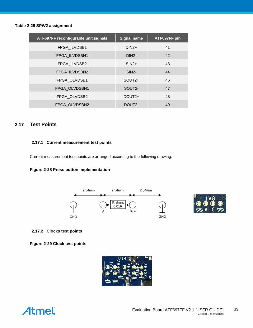
2.17 Test Points
2.17.1 Current measurement test points
Current measurement test points are arranged according to the following drawing:
Figure 2-28 Press button implementation
2.17.2 Clocks test points
Figure 2-29 Clock test points
2.54mm 2.54mm 2.54mm
GND GND
R shunt 0.01R
A B, C
Evaluation Board ATF697FF V2.1 [USER GUIDE] 41002D – AERO 01/16
40
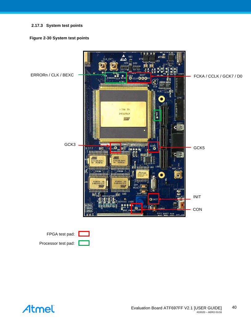
2.17.3 System test points
Figure 2-30 System test points
ERRORn / CLK / BEXC FCKA / CCLK / GCK7 / D0
GCK5
INIT
CON
GCK3
FPGA test pad:
Processor test pad:
Evaluation Board ATF697FF V2.1 [USER GUIDE] 41002D – AERO 01/16
41
2.18 Expansion connector
Expansion connector manufacturer: SAMTEC
Expansion connector reference: QTH-090-02-L-D-A
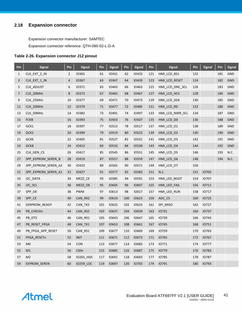
Table 2-26. Expansion connector J12 pinout
Pin Signal Pin Signal Pin Signal Pin Signal Pin Signal Pin Signal Pin Signal
1 CLK_EXT_2_IN 2 IO365 61 IO431 62 IO433 121 HMI_LCD_BS1 122 181 GND
3 CLK_EXT_1_IN 4 IO367 63 IO347 64 IO439 123 HMI_LCD_RESET 124 182 GND
5 CLK_ADJUST 6 IO371 65 IO443 66 IO463 125 HMI_LCD_DNC_SCL 126 183 GND
7 CLK_20MHz 8 IO373 67 IO465 68 IO467 127 HMI_LCD_NCS 128 184 GND
9 CLK_25MHz 10 IO377 69 IO471 70 IO473 129 HMI_LCD_SDA 130 185 GND
11 CLK_33MHz 12 IO379 71 IO477 72 IO485 131 HMI_LCD_RD 132 186 GND
13 CLK_50MHz 14 IO383 73 IO491 74 IO497 133 HMI_LCD_NWR_SCL 134 187 GND
15 FCKB 16 IO393 75 IO503 76 IO507 135 HMI_LCD_D0 136 188 GND
17 GCK1 18 IO397 77 IO513 78 IO517 137 HMI_LCD_D1 138 189 GND
19 GCK2 20 IO399 79 IO519 80 IO523 139 HMI_LCD_D2 140 190 GND
21 GCK6 22 IO405 81 IO527 82 IO531 141 HMI_LCD_D3 142 191 GND
23 GCK8 24 IO413 83 IO533 84 IO539 143 HMI_LCD_D4 144 192 GND
25 CLK_GEN_CS 26 IO417 85 IO545 86 IO551 145 HMI_LCD_D5 146 193 N.C.
27 SPP_EEPROM_SEREN_B 28 IO419 87 IO557 88 IO559 147 HMI_LCD_D6 148 194 N.C.
29 SPP_EEPROM_SEREN_A2 30 IO423 89 IO565 90 IO571 149 HMI_LCD_D7 150
31 SPP_EEPROM_SEREN_A1 32 IO427 91 IO577 92 IO583 151 N.C. 152 IO705
33 I2C_DATA 34 MEZZ_CE 93 IO585 94 IO591 153 HMI_LED_BOOT 154 IO707
35 I2C_SCL 36 MEZZ_OE 95 IO605 96 IO607 155 HMI_LED_FAIL 156 IO711
37 SPP_OE 38 PWM 97 IO613 98 IO017 157 HMI_LED_RUN 158 IO717
39 SPP_CE 40 CAN_RX2 99 IO619 100 IO623 159 ADC_CS 160 IO725
41 EERPROM_READY 42 CAN_TX2 101 IO625 102 IO633 161 SPI_MISO 162 IO727
43 PB_CHECKn 44 CAN_RS2 103 IO637 104 IO639 163 IO731 164 IO737
45 PB_OTS 46 CAN_RX1 105 IO643 106 IO647 165 IO739 166 IO743
47 PB_RESET_FPGA 48 CAN_TX1 107 IO653 108 IO661 167 IO745 168 IO751
49 PB_FPGA_APP_RESET 50 CAN_RS1 109 IO677 110 IO669 169 IO759 170 IO763
51 FPGA_RESETn 52 INIT 111 IO671 112 IO673 171 IO765 172 IO767
53 M0 54 CON 113 IO677 114 IO683 173 IO771 174 IO777
55 M1 56 CS0n 115 IO685 116 IO687 175 IO779 176 IO783
57 M2 58 IO265_HDC 117 IO691 118 IO693 177 IO785 178 IO787
59 EEPROM_SEREN 60 IO259_LDC 119 IO697 120 IO703 179 IO791 180 IO793
Evaluation Board ATF697FF V2.1 [USER GUIDE] 41002D – AERO 01/16
42
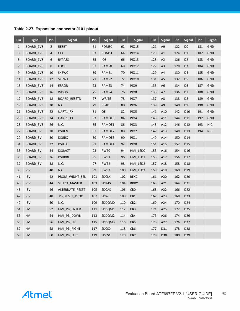
Table 2-27. Expansion connector J101 pinout
Pin Signal Pin Signal Pin Signal Pin Signal Pin Signal Pin Signal Pin Signal
1 BOARD_1V8 2 RESET 61 ROMS0 62 PIO15 121 A0 122 D0 181 GND
3 BOARD_1V8 4 CLK 63 ROMS1 64 PIO14 123 A1 124 D1 182 GND
5 BOARD_1V8 6 BYPASS 65 IOS 66 PIO13 125 A2 126 D2 183 GND
7 BOARD_1V8 8 LOCK 67 RAMS0 68 PIO12 127 A3 128 D3 184 GND
9 BOARD_1V8 10 SKEW0 69 RAMS1 70 PIO11 129 A4 130 D4 185 GND
11 BOARD_1V8 12 SKEW1 71 RAMS2 72 PIO10 131 A5 132 D5 186 GND
13 BOARD_3V3 14 ERROR 73 RAMS3 74 PIO9 133 A6 134 D6 187 GND
15 BOARD_3V3 16 WDOG 75 RAMS4 76 PIO8 135 A7 136 D7 188 GND
17 BOARD_3V3 18 BOARD_RESETN 77 WRITE 78 PIO7 137 A8 138 D8 189 GND
19 BOARD_3V3 20 N.C. 79 READ 80 PIO6 139 A9 140 D9 190 GND
21 BOARD_3V3 22 UART1_RX 81 OE 82 PIO5 141 A10 142 D10 191 GND
23 BOARD_3V3 24 UART1_TX 83 RAMOE0 84 PIO4 143 A11 144 D11 192 GND
25 BOARD_3V3 26 N.C. 85 RAMOE1 86 PIO3 145 A12 146 D12 193 N.C.
27 BOARD_5V 28 DSUEN 87 RAMOE2 88 PIO2 147 A13 148 D13 194 N.C.
29 BOARD_5V 30 DSURX 89 RAMOE3 90 PIO1 149 A14 150 D14
31 BOARD_5V 32 DSUTX 91 RAMOE4 92 PIO0 151 A15 152 D15
33 BOARD_5V 34 DSUACT 93 RWE0 94 HMI_LED0 153 A16 154 D16
35 BOARD_5V 36 DSUBRE 95 RWE1 96 HMI_LED1 155 A17 156 D17
37 BOARD_5V 38 N.C. 97 RWE2 98 HMI_LED2 157 A18 158 D18
39 -5V 40 N.C. 99 RWE3 100 HMI_LED3 159 A19 160 D19
41 -5V 42 PROM_WIDHT_SEL 101 SDCLK 102 BEXC 161 A20 162 D20
43 -5V 44 SELECT_MASTER 103 SDRAS 104 BRDY 163 A21 164 D21
45 -5V 46 ALTERNATE_RESET 105 SDCAS 106 CB0 165 A22 166 D22
47 -5V 48 PB_RESET_PROC 107 SDWE 108 CB1 167 A23 168 D23
49 -5V 50 N.C. 109 SDDQM0 110 CB2 169 A24 170 D24
51 HV 52 HMI_PB_ENTER 111 SDDQM1 112 CB3 171 A25 172 D25
53 HV 54 HMI_PB_DOWN 113 SDDQM2 114 CB4 173 A26 174 D26
55 HV 56 HMI_PB_UP 115 SDDQM3 116 CB5 175 A27 176 D27
57 HV 58 HMI_PB_RIGHT 117 SDCS0 118 CB6 177 D31 178 D28
59 HV 60 HMI_PB_LEFT 119 SDCS1 120 CB7 179 D30 180 D29
Evaluation Board ATF697FF V2.1 [USER GUIDE] 41002D – AERO 01/16
43
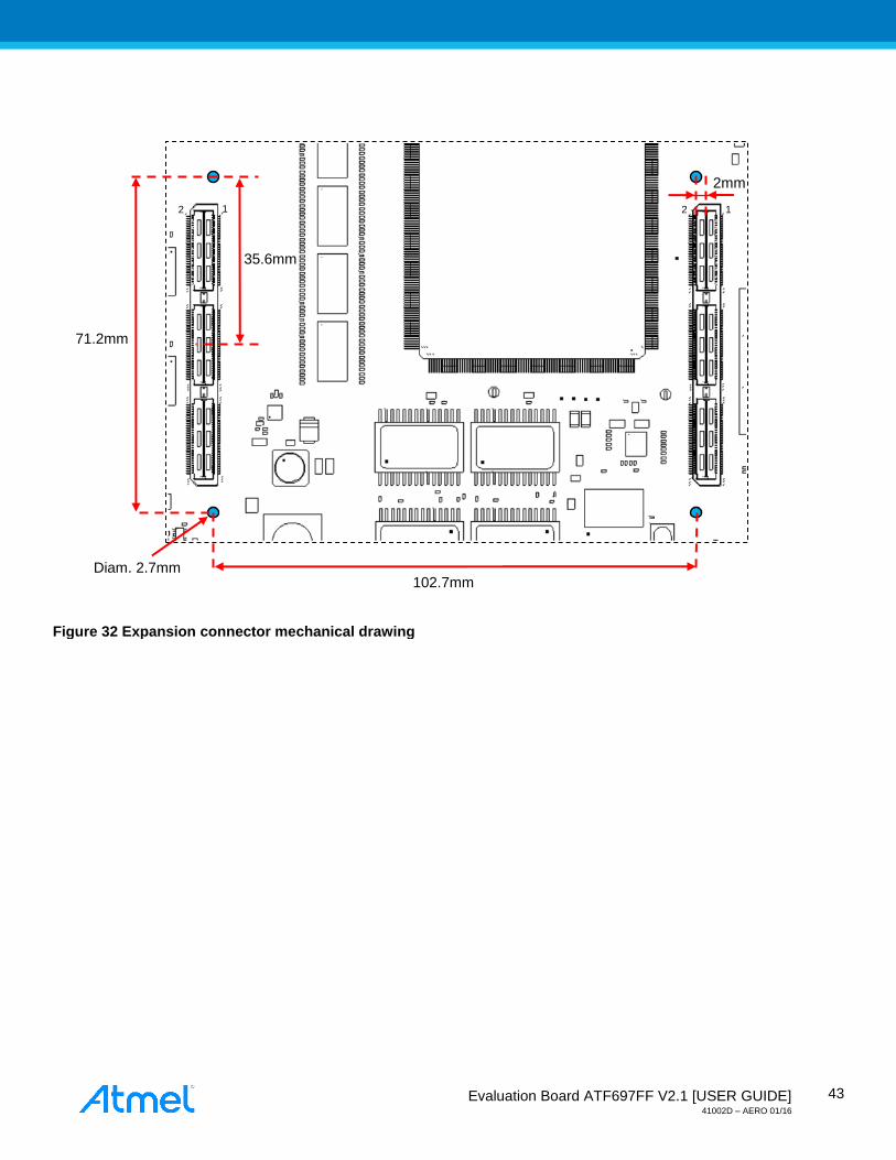
71.2mm
102.7mm Diam. 2.7mm
2mm
35.6mm
1 2 2 1
Figure 32 Expansion connector mechanical drawing
Evaluation Board ATF697FF V2.1 [USER GUIDE] 41002D – AERO 01/16
44
3. Appendix A – Space Programmer Update
See troubleshooting document (41044B) if a space programmer firmware update is needed.
Evaluation Board ATF697FF V2.1 [USER GUIDE] 41002D – AERO 01/16
45
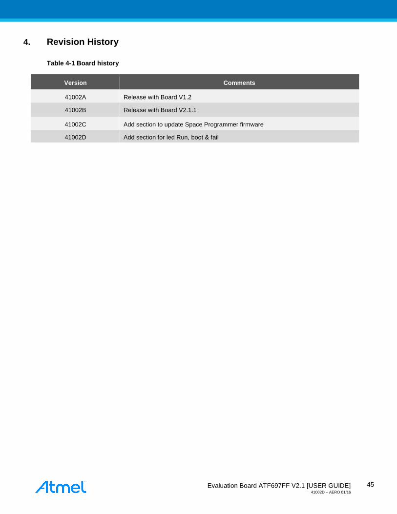
4. Revision History
Table 4-1 Board history
Version Comments
41002A Release with Board V1.2
41002B Release with Board V2.1.1
41002C Add section to update Space Programmer firmware
41002D Add section for led Run, boot & fail

Atmel Corporation
2325 Orchard Parkway
San Jose, CA 95131
USA
Tel: (+1)(408) 441-0311
Fax: (+1)(408) 487-2600
www.atmel.com
Atmel Asia Limited
Unit 01-5 & 16, 19F
BEA Tower, Millennium City 5
418 Kwun Tong Road
Kwun Tong, Kowloon
HONG KONG
Tel: (+852) 2245-6100
Fax: (+852) 2722-1369
Atmel Munich GmbH
Business Campus
Parkring 4
D-85748 Garching b. Munich
GERMANY
Tel: (+49) 89-31970-0
Fax: (+49) 89-3194621
Atmel Japan G.K.
16F Shin-Osaki Kangyo Building
1-6-4 Osaki
Shinagawa-ku, Tokyo 141-0032
JAPAN
Tel: (+81)(3) 6417-0300
Fax: (+81)(3) 6417-0370
© 2013 Atmel Corporation. All rights reserved. / Rev.: Error! Reference source not found.2013
Atmel®, Atmel logo and combinations thereof, Enabling Unlimited Possibilities®, and others are registered trademarks or trademarks of Atmel Corporation or its
subsidiaries. Other terms and product names may be trademarks of others.
Disclaimer: The information in this document is provided in connection with Atmel products. No license, express or implied, by estoppel or otherwise, to any intellectual property right is granted by this document or in connection with the sale of Atmel products. EXCEPT AS SET FORTH IN THE ATMEL TERMS AND CONDITIONS OF SALES LOCATED ON THE ATMEL WEBSITE, ATMEL ASSUMES NO LIABILITY WHATSOEVER AND DISCLAIMS ANY EXPRESS, IMPLIED OR STATUTORY WARRANTY RELATING TO ITS PRODUCTS INCLUDING, BUT NOT LIMITED TO, THE IMPLIED WARRANTY OF MERCHANTABILITY, FITNESS FOR A PARTICULAR PURPOSE, OR NON-INFRINGEMENT. IN NO EVENT SHALL ATMEL BE LIABLE FOR ANY DIRECT, INDIRECT, CONSEQUENTIAL, PUNITIVE, SPECIAL OR INCIDENTAL DAMAGES (INCLUDING, WITHOUT LIMITATION, DAMAGES FOR LOSS AND PROFITS, BUSINESS INTERRUPTION, OR LOSS OF INFORMATION) ARISING OUT OF THE USE OR INABILITY TO USE THIS DOCUMENT, EVEN IF ATMEL HAS BEEN ADVISED OF THE POSSIBILITY OF SUCH DAMAGES. Atmel makes no representations or warranties with respect to the accuracy or completeness of the contents of this document and reserves the right to make changes to specifications and products descriptions at any time without notice. Atmel does not make any commitment to update the information contained herein. Unless specifically provided otherwise, Atmel products are not suitable for, and shall not be used in, automotive applications. Atmel products are not intended, authorized, or warranted for use as components in applications intended to support or sustain life.