Document
67
1 CHAPTER-1 INTRODUCTION MEMS is a process technology used to create tiny integrated devices or systems that combine mechanical and electrical components. They are fabricated using integrated circuit (IC) batch processing techniques and can range in size from a few micrometers to millimetres. These devices (or systems) have the ability to sense, control and actuate on the micro scale, and generate effects on the macro scale. The interdisciplinary nature of MEMS utilizes design, engineering and manufacturing expertise from a wide and diverse range of technical areas including integrated circuit fabrication technology, mechanical engineering, materials science, electrical engineering, chemistry and chemical engineering, as well as fluid engineering, optics, instrumentation and packaging. The complexity of MEMS is also shown in the extensive range of markets and applications that incorporate MEMS devices. MEMS can be found in systems ranging across automotive, medical, electronic, communication and defence applications. Current MEMS devices include accelerometers for airbag sensors, inkjet printer heads, computer disk drive read/write heads, projection display chips, blood pressure sensors, optical switches, microvalves, biosensors and many other products that are all manufactured and shipped in high commercial volumes. MEMS has been identified as one of the most promising technologies for the 21 st Century and has the potential to revolutionize both industrial and consumer products by combining siliconbased microelectronics with micromachining technology. Its techniques and microsystembased devices
-
Upload
vasanthlogarajl -
Category
Documents
-
view
7 -
download
1
description
doc
Transcript of Document

1
CHAPTER-1
INTRODUCTION
MEMS is a process technology used to create tiny integrated devices
or systems that combine mechanical and electrical components. They are
fabricated using integrated circuit (IC) batch processing techniques and can
range in size from a few micrometers to millimetres. These devices (or
systems) have the ability to sense, control and actuate on the micro scale,
and generate effects on the macro scale.
The interdisciplinary nature of MEMS utilizes design, engineering
and manufacturing expertise from a wide and diverse range of technical
areas including integrated circuit fabrication technology, mechanical
engineering, materials science, electrical engineering, chemistry and
chemical engineering, as well as fluid engineering, optics, instrumentation
and packaging. The complexity of MEMS is also shown in the extensive
range of markets and applications that incorporate MEMS devices. MEMS
can be found in systems ranging across
automotive, medical, electronic, communication and defence applications.
Current MEMS devices include accelerometers for airbag sensors, inkjet
printer heads, computer disk drive read/write heads, projection display chips,
blood pressure sensors, optical switches, microvalves, biosensors and many
other products that are all manufactured and shipped in high commercial
volumes.
MEMS has been identified as one of the most promising technologies
for the 21st Century and has the potential to revolutionize both industrial and
consumer products by combining siliconbased microelectronics with
micromachining technology. Its techniques and microsystembased devices
2
have the potential to dramatically affect of all of our lives and the way we
live. If semiconductor micro fabrication was seen to be the first micro
manufacturing revolution, MEMS is the second revolution.
The field of MEMS has been divided into four main sections. In the
first section, the reader is introduced to MEMS, its definitions, history,
current and potential applications, as well as the state of the MEMS market
and issues concerning miniaturization. The second section deals with the
fundamental fabrication methods of MEMS including photolithography,
bulk micromachining, surface micromachining and high-aspect-ratio
micromachining, assembly, system integration and packaging of MEMS
devices is also described here. The third section reviews the range of MEMS
sensors and actuators, the phenomena that can be sensed or acted upon with
MEMS devices, and a brief description of the basic sensing and actuation
mechanisms. The final section illustrates the challenges facing the MEMS
industry for the commercialisation and success of MEMS.
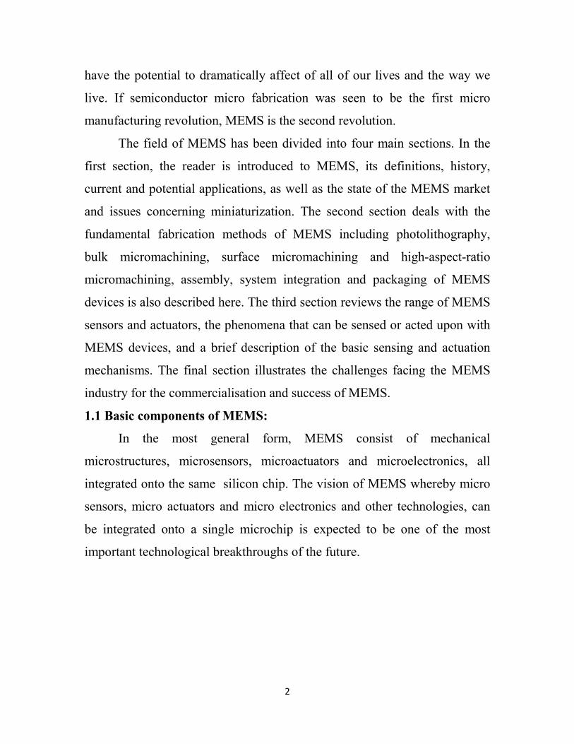
1.1 Basic components of MEMS:
In the most general form, MEMS consist of mechanical
microstructures, microsensors, microactuators and microelectronics, all
integrated onto the same silicon chip. The vision of MEMS whereby micro
sensors, micro actuators and micro electronics and other technologies, can
be integrated onto a single microchip is expected to be one of the most
important technological breakthroughs of the future.

3
Figure 1.1 Components of MEMS
1.1.1 Micro sensors
A very small sensor with physical dimensions in the submicrometer to
millimeter range. Over the past several decades MEMS researchers and
developers have demonstrated an extremely large number of micro sensors
for almost every possible sensing modality including temperature, pressure,
inertial forces, chemical species, magnetic field, radiation, etc. Remarkably,
many of these micro machined sensors have demonstrated performances
exceeding those of their macro scale counterparts.
Sensors are an essential element in many measurement, process, and
control systems, with countless applications in the automotive, aerospace,
biomedical, telecommunications, environmental, agricultural, and other
industries. The stimulus to miniaturize sensors lies in the enormous cost
benefits that are gained by using semiconductor processing technology, and
in the fact that microsensors are generally able to offer a better sensitivity,
accuracy, dynamic range, and reliability, as well as lower power
consumption, than their larger counterparts. Mechanical microsensors form
perhaps the largest family of microsensors because of their widespread
availability. Microsensors have been produced to measure a wide range of

4
mechanical properties, including force, pressure, displacement, acceleration,
rotation, and mass flow. Force sensors generally use a sensing element that
converts the applied force into the deformation of the elastic element.
Applications for chemical and biochemical microsensors are
environmental monitoring and medicine. Only a few such devices now exist.
Examples include a glucose biochemical microsensor and ion-selective
field-effect devices used to measure blood pH. The use of microsensors to
gather medical diagnostic information is an attractive proposition, and
eventually there may even be implanted microsensors to diagnose health
problems, using smell-sensitive array devices. In the case of micro sensor,
the device typically converts a measured mechanical signal into an electrical
signal.
1.1.2 Micro electronics
In microelectronics and MEMS industry you need to observe, analyze,
and identify the characteristics of your products. This is equally true in
process control and failure analysis. The knowledge of your device’s
physical structure is vital in understanding the process. Development of
microelectronics and design of mechanical microsystems (MEMS) rely on
efficient microscopes. Any number of functional features such as cracks,
voids or connections can be investigated. In the creation of miniaturized
mechanical devices, light microscopy serves as your tool for assessing
prototypes and monitoring results of precision machining. The increasing
integration of microelectronics into the nanometer area makes it necessary
for you to examine these structures with scanning electron microscopes.
SEM deliver resolutions in the nanometer range and large depth of field,
5
resulting in brilliant images and precise circuit editing and analysis. Circuit
editing with FIB-SEM even allows to fabricate complex structures.
1.1.3 Micro structures
Microstructure is defined as the structure of a prepared surface or
thin foil of material as revealed by a microscope. The microstructure of a
material (which can be broadly classified into metallic, polymeric, ceramic
and composite) can strongly influence physical properties such as strength,
toughness, ductility, hardness, corrosion resistance, high/low temperature
behavior, wear resistance, and so on, which in turn govern the application of
these materials in industrial practice. Microstructure at scales smaller than
can be viewed with optical microscopes is often called ultrastructure or
nanostructure.
1.1.4 Micro actuators
Micro actuators are important building blocks for many MEMS
devices, which generate forces or displacements to realize scanning, tuning,
manipulating or delivering function.Micro electrostatic actuators are more
popular than others due to their high compatibility with mature micro
fabrication processes, low power consumption, simple structures and quick
response.
1.1.5 Actuators
An actuator is a type of motor that is responsible for moving or
controlling a mechanism or system. It is operated by a source of energy,
typically electric current, hydraulic fluid pressure, or pneumatic pressure,
6
and converts that energy into motion. An actuator is the mechanism by
which a control system acts upon an environment. The control system can be
simple (a fixed mechanical or electronic system), software-based (e.g. a
printer driver, robot control system), a human, or any other input. Actuators
are a type of tool which is used to put something into automatic action. It is
used on a wide variety of sources, from humans putting something into
action to computers starting up a program.
There are several reasons why actuators may be used in an office
work area. Most of these will be used as the thing that positions or moves a
certain object. For example, many will be used to move or position valve
doors in certain systems. They may also be used to maneuver certain
mechanical devices that are used in a work area. By using actuators, it is
easier for one to work in their area, as well as easier to maneuver something
around in the certain area.
1.2 Materials for MEMS
1.2.1 Silicon
One of very few materials that can be economically manufactured in
single crystal Substrates. It is a Diamond lattice.
Figure 1.2 Diamond structure
7
In silicon crystal orientation, each site is tetrahedrally coordinated
with four other sites in the other sublattice. It has properties such as extensive studies and documentation, Suitable for electronic, mechanical,
thermal, and optical integration.It can sustain harsh (mechanical) handling
conditions and mechanical properties are uniform across wafer lots. It has
structures like crystalline, polycrystalline-polysilicon, amorphous.
1.2.2 SiO2/Quartz/Glass
The stable oxide is one of the key elements for the success of silicon
in IC,Excellent thermal and electrical insulation, Sacrificial layers in surface
micromachining processes.
a) SiO2
Fused silica is a purer version of fused quartz that is made
synthetically from various Silicon gasses. It has 17 crystalline phases.
b) Quartz
It is a single crystal material, low impurity concentration. Fused
quartz is the amorphous form of quartz. It is made from natural crystalline
quartz, usually quartz sand that has been mined.
c) Glass
A glass is an amorphous solid, impurities, low melting temperature.
Like most glasses, the dominant component of Borosilicate glass is SiO2
with boron and various other elements added to give it its excellent qualities.
1.2.3 Polymers
Spin coated with varying thickness; few nm – hundreds of microns. It
is used in sensing of chemical gases and humidity. It is used as Photoresists.
Epoxy based photoresist can form layers up to 100 µm. It is of low cost.
8
1.3 MEMS Fabrication process
a) Photolithography steps
• Photoresist spinnning, 1-10 µm spin coating.
• Optical exposure through a photomask.
• Developing to dissolve exposed resist.
• Bake to drive off solvents.
• Remove using solvents (acetone) or O2 plasma.
b) Photoresist application
Spin-casting photoresist
• Polymer resin, sensitizer, carrier solvent.
• Positive and negative photoresist.
1.4 Micromachining
1.4.1 Bulk micromachining
Bulk micromachining involves the removal of part of the bulk
substrate. It is a subtractive process that uses wet anisotropic etching or a dry
etching method such as reactive ion etching (RIE), to create large pits,
grooves and channels. Materials typically used for wet etching include
silicon and quartz, while dry etching is typically used with silicon, metals,
plastics and ceramics.
a)Wet etching
Wet etching describes the removal of material through the immersion
of a material (typically a silicon wafer) in a liquid bath of a chemical
etchant. These etchants can be isotropic or anisotropic. Isotropic etchants
etch the material at the same rate in all directions, and consequently remove
material under the etch masks at the same rate as they etch through the
material and this is known as undercutting.

9
b)Dry etching
Dry etching relies on vapour phase or plasma-based methods of
etching using suitably reactive gases or vapours usually at high
temperatures. The most common form for MEMS is reactive ion etching
(RIE) which utilizes additional energy in the form of radio frequency power
to drive the chemical reaction. Energetic ions are accelerated towards the
material to be etched within a plasma phase supplying the additional energy
needed for the reaction; as a result the etching can occur at much lower
temperatures than those usually needed.

10
CHAPTER 2
LITERATURE SURVEY
2.1 “Carbon nanotube sensors for exhaled breath components”,
(Oleksandr Kuzmych, Brett L Allen and Alexander Star Published 22
August 2007)
In this project the detection of nitric oxide (NO) in gas phase is based
on a combination of acidic gas scrubbing, oxidation, and conductivity
measurements using a chemically functionalized carbon nanotube field-
effect transistor (NTFET) device. Gas mixtures containing NO are passed
through an Ascarite scrubber and then an oxidizing material (CrO3) which
converts NO into NO2. The latter is delivered to the surface of the NTFET
sensor coated with poly ethylene imine(PEI) polymer. The wide range of
NO gas concentrations from about 2 ppb up to 5 ppm was tested. The
primary reason for this interest involves the role NO molecules play in
biological function .
This proposed syetem used NTFET devices comprised of a network of
single-walled carbon nanotubes (SWNTs) contacted by Au/Ti metal
electrodes representing the source (S) and drain (D) with a Si back gate
separated by SiO2 in a FET configured circuit. S–D conductance versus gate
voltage (G–VG) plots are obtained, the transfer characteristic of a typical
NTFET device used in this paper. Devices exhibit p-type characteristics in
ambient conditions with positive threshold voltage values and low on/off
ratios, which are characteristic to network NTFET devices with 5 μm
separations . Presence of analytes or chemical modification of NTFETs
results in a change of conductance which is evident in the n-type NTFET

11
character after PEI coating (vide infra).Here, PEI increases the sensitivity to
converted NO, and RH and CO2 affect the sensor response. This sensor
poses the advantages of real time measurements, along with low costs and
high sensitivity.
2.2 “MEMS based gas sensor for monitoring process chambers in
semiconductor manufacturing”, (Ijaz H. Jafria, Frank DiMeo Jr. b, Jeffrey
Neunerb, Sue DiMascio b, and James Marchettia IntelliSense Corporation
MA 01887b Advanced Technology Materials, Inc., 7 Commerce Drive,
Danbury, CT 06810 Published in 2000)
In this project a commercial software package IntelliSuiteTM was
used to speed the design and optimization of gas sensors. This is used to
model the coupled thermo-electro-mechanical responses of devices known
as microhotplates. Models were built based on the GDSII formatted mask
layout, process sequences, and layer thicknesses.The modeling results from
this study predict that the first three resonant frequency modes for these
devices are in the 612 to1530 kHz range for an all pinned device, and 134 to
676 kHz for a springboard arrangement. This process also involves the FEA
model creation and Microhotplate generation. This analysis consisted of the
creation of the 3D finite element mesh, verification of the consistency of the
model mesh size. In this work the finite element modeling is used to predict
the coupled thermo-electro-mechanical properties of CMOS based
microhotplates. The measured thickness of the thin film layers as inputs to
the model, and calculated the resonant frequency as a function of absorbed
mass. The analyses predict that the first three modes of natural frequency are
612, 1522, and 1530 kHz for the four post device, and 134, 382, and 676
kHz for a two post, or springboard arrangement. The simulation results agree

12
very well with the experimental data at low power. At higher power,
however, the model and experimental results begin to diverge and are
currently working on improving the model by incorporating these effects.
2.3 “Single walled and multi walled carbon nanotube structure,
synthesis and applications”, (E.N. Ganesh, This project appear in the
International Journal of Innovative Technology and Exploring Engineering
(IJITEE) ISSN: 2278-3075, Volume-2, Issue-4, March 2013)
Carbon Nanotubes have exceptional mechanical and electrical
properties. Various methods have been thoroughly investigated for the
growth of CNTs. The best and the most commonly used method is Chemical
Vapour Deposition (CVD). The structural uniformity of carbon nanotubes
produced by plasma enhanced Chemical Vapour Deposition gives uniform
height and diameter. This paper discussed about Comparison of different
methods about synthesis of carbon nano tube, Structure of SWNT, DWNT
and MWNT carbon nano tube, Simulation of carbon nano tubes with
different distortions and the properties of carbon nano tube for Energy
storage and Medical applications. Carbon nanotubes (CNTs) are hollow
cylinders of carbon atoms . There are two types of nanotubes: single-walled
nanotubes (SWNTs) and multiwalled nanotubes (MWNTs), which differ in
the arrangement of their graphene cylinders. Here, The single layer and
multi layer Carbon nano tube using nano explorer tool was simulated.The
simulated properties of CNT would be used for energy storage purpose as
well for transmission of electrical energy. Though it is known that CNT’s
have high aspect ratio, Young’s modulus over one terra pascal, Tensile
strength of 200 Giga pascal. It describes about the advantage of plasma
enhanced CVD technique and the simulation of CNT structure also

13
described. So, that the structural parameters of types of CNTs was calculated
and also various tube distortion in CNT and calculated energy per atom with
respect to radius also mentioned.
2.4 “Ultra sensitive and highly selective gas sensors using three-
dimentional tungsten oxide nanowire networks”, (Andrea Ponzoni, Yong
Ding published in 15 May 2006)
Three-dimensional 3D tungsten oxide nanowire networks have been
demonstrated as a high-surface area material for building ultrasensitive and
highly selective gas sensors. Utilizing the 3D hierarchical structure of the
networks, high sensitivity has been obtained towards NO2, revealing the
capability of the material to detect concentration as low as 50 ppb (parts per
billion). The results highlight that the nanobelts, nanowires technology can
be adopted for the development of gas.The performance of a solid-state gas
sensor is characterized by its sensitivity, stability and selectivity. The
working principle relies on modulation of electrical conductivity due to
surface oxidation ,reduction caused by gas exposure. Because, only the
surface layer is affected by such reactions, the sensitivity is strongly
dependent on the surface-to-volume ratio of the material used. This purpose
has been pursued by synthesizing layers with a porous morphology to
enhance the material surface area. Porosity is enhanced by means of the
thick film synthesis approach typically adopted in the gas sensing field. Such
high porosity is not easy to achieve by thin film approach. Another approach
largely used in the field is the rheotaxial growth and its thermal oxidation
RGTO method, which allows synthesizing a porous thin film monolayer
composed of nano sized grains. As far as grain size is concerned, it has to be
kept in the order of or lower than the debye length, which is the depth into

14
the surface that the chemisorption process can effectively modify the
electrical properties of the metal oxide material. The proposed system
describes gas sensing performances of three-dimensional WO3−x nanowire
networks. This material can be applied in gas sensing field to develop NO2
sensors with performances suitable for practical application.
2.5 Summary
Asthma is a chronic disease which will interfere with a
person’s daily functioning. This literature review has following disadvantage
like complexity, large size and accuracy. The COMSOL Software didn’t
provide fast response. Its suits only for mechanical applications. The main
disadvantages selectivity and sensitivity. So to overcome the selectivity
problem the CNT gas sensor is designed and the size is also reduced. That
will be explained in upcoming chapters.

15
CHAPTER 3
EXISTING SYSTEM
3.1 Introduction
This project reports on a novel miniaturized MEMS-based
amperometric nitric oxide sensor that is suitable for a point of care testing
device for asthma. The novelty lies in the combination of a high surface area
microporous structured electrode, nano-structured Nafion that is coated on
the side walls of the micropores, and liquid electrolyte. This combination
allows detection of very low concentration gas, has a high sensitivity of and
has both a response and a recovery time of 6 s. The sensor is integrated with
a PCB potentiostat to form a complete measuring module. The limit of
detection of this sensor was estimated to be 0.3ppb. An ideal sensor for
breath analysis should have low detection limit (<1 ppb), fast response, must
work in varying humidity, should have repeatability and should be batch
manufacturable. All these features are required for manufacturing a portable
gas monitoring equipment that can be used for in situ measurement of nitric
oxide gas.
Sensors using electrochemical methods have previously been
developed to meet the demand of very low concentration detection. However
for measurements of eNO, they lack important features such as fast
response, small size and high sensitivity. Although conventional
electrochemical sensors can detect down to single ppb gas concentration
they suffer from a long response time, typically in the order of 60-100 s.
consequently they require complicated flow handling and buffering of the
exhaled breath sample. Most of the miniaturized NO sensors are realized
using metal oxide as the sensing material and have limited detection range of

16
1-100 ppm. Amperometric detection techniques using only solid polymer
electrolyte (SPE) like Nafion has been shown to detect NO but the detection
limit of 5 ppm is not useful for asthma detection . Amperometric sensors
with liquid electrolyte have modified electrodes of carbon or platinum to
have high sensitivity, but the sensor cannot be batch manufactured using
standard processing technology. In this project, a novel MEMS-based
amperometric nitric oxide sensor that has been designed to meet the required
criteria for a portable asthma detector.
3.2 Concept
The designed sensor works on the principle of amperometric detection
of the analyte. The oxidation of the analyte at the working electrode results
in a current that is detected by using a potentiostat that consists of a
transimpedance amplifier. It is also used for maintaining a constant potential
between the working and the reference electrode. The working electrode is
fabricated by etching silicon to form microporous structure. It is covered
with Al2O3 that is deposited by using atomic layer deposition, which is
followed by the deposition of platinum. The Al2O3 acts as an insulator
between the silicon and the platinum. The microporous structure thus
prepared is then covered with a thin layer of Nafion. The Nafion layer is the
diffusion layer that permits the gas, electrode and liquid interaction. This
interaction leads to the oxidation of the nitric oxide molecule causing a
current flow between the working and counter electrode. This current is
measured by using a PCB based potentiostat.
The counter electrode enables a current to flow through the sensor
cell. The working potential, electrolyte and electrode materials are so chosen
that the gas being measured is oxidized at the working electrode. As the
oxidization takes place at the working electrode, oxygen is normally reduced

17
to water at the counter electrode. The resulting current which flows through
the sensor is directly proportional to the gas concentration.A micromachined
working electrode is fabricated and mounted together with the reference and
counter electrode.
3.3 Fabrication
The working electrode is fabricated using a double side polished
100mm, 300 μm thick silicon wafer. The silicon wafer is spin coated with 6
μm thick photoresist (AZ 9260). The wafer is then soft baked on a hot plate
for 2 min and is exposed with UV intensity of 300 mW/cm2 for 15 s. The
photoresist is developed using developer 2401 for 3 min in order to define a
pattern. The pattern defines the working electrode area. The grid pattern is 6
mm in diameter and has triangular micropores of 120 μm. The grid width is
approximately 20 μm. The grid pattern is then etched using deep reactive ion
etching for 1.5 hrs to form a microporous structure .
Figure 3.1.a Photoresist patterning and silicon grid etching

18
Figure 3.1.b Photoresist removal and Al2O3 deposition followed by Pt
deposition using atomic layer deposition(ALD)
The etched silicon wafer is then transferred to an atomic layer
deposition chamber. Here a 10 nm layer of Al2O3 is deposited on the wafer
followed by a 10 nm thick platinum layer. The Al2O3 acts as an insulator
between the platinum (Pt) and the silicon. The platinum layer is the sensing
electrode for the gas sensor. The wafer is then diced into 1 cm x 1 cm sized
chips.
Figure 3.1.c The wafer is diced in 1cm×1cm chips followed by
Nafion coating on individual chips
Figure 3.1.d SEM picture showing a top view of a grid membrane
19
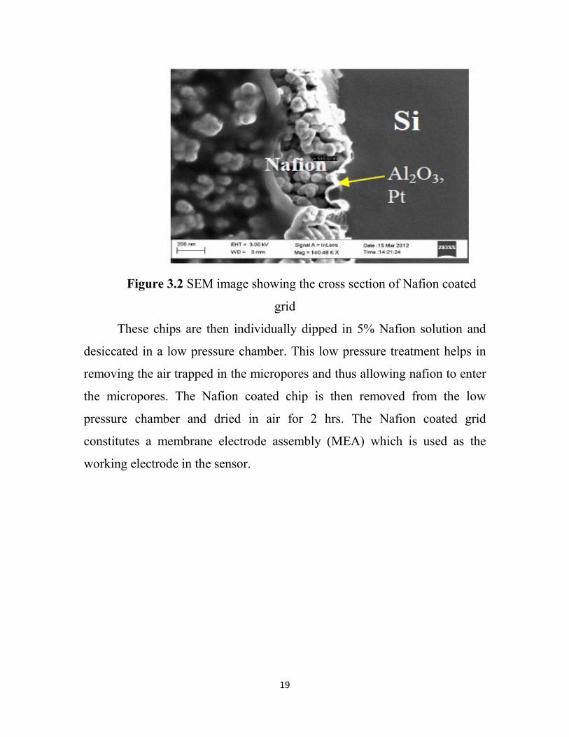
Figure 3.2 SEM image showing the cross section of Nafion coated
grid
These chips are then individually dipped in 5% Nafion solution and
desiccated in a low pressure chamber. This low pressure treatment helps in
removing the air trapped in the micropores and thus allowing nafion to enter
the micropores. The Nafion coated chip is then removed from the low
pressure chamber and dried in air for 2 hrs. The Nafion coated grid
constitutes a membrane electrode assembly (MEA) which is used as the
working electrode in the sensor.

20
Figure 3.3 NO sensor on a polycarbonate substrate and silver on
counter and reference electrode
The fabrication of the counter and reference electrode is carried out on
a 2 mm thick polycarbonate (PC) substrate. Silver of thickness 500 nm is
deposited on one side of the PC substrate using e-beam evaporation. The
silver is then patterned using a milling machine to define counter and
reference electrode. The reference electrode is oxidized to AgO2. This is
done by applying a voltage of 1.0 V on the silver electrode, which is the
anode by using a platinum electrode as the cathode. The stability of this
electrode is tested in H2SO4 solution. Nitrogen and air is bubbled alternately
into the solution and the open circuit potential of the silver electrode with
respect to a standard calomel electrode is measured.
The Open Circuit Potential (OCP) at this electrode was observed to
be stable. The oxidized silver electrode is used as the reference electrode in
the set-up. To compensate for the evaporation of the electrolyte through the
working electrode, a 1 mm wide and 1 mm deep channel is milled on the
back side of the PC substrate and this channel is sealed with another 1 mm
21
thick polycarbonate cover. The channel is used as a connection between the
electrolyte filling port and the electrolyte chamber. This ensures a
continuous supply of electrolyte to the electrolyte chamber.
The working electrode chip is glued on top of the counter and the
reference electrode by using acid resistant silicone epoxy. A gap of 500 μm
is maintained between the working electrode and the counter/reference
electrode by using a spacer frame made of oxidized silicon. The epoxy is
cured in air for about 1 hr. The assembly is then submerged into the
electrolyte solution and put in a vacuum desiccator so that the electrolyte
fills the channels and the chamber between the working and the
counter/reference electrode. The electrolyte now ionically connects the
working, counter and the reference electrodes.
3.4 Advantages
A micromachined nitric oxide sensor has a fast response, is
highly sensitive and stable.
This sensor is potentially suitable for use in point of care testing
in asthma diagnostics.
The NO sensor has high sensitivity in detection of Nitric Oxide.
This also allows fast response and recovery time of 6 s.
This work demonstrates the potential for miniaturized MEMS-
based electrochemical gas sensors with very high fast response
time, enabling sensing in portable devices.

22
3.5 Disadvantages
The micro machined nitric oxide sensor has selectivity
problem,because it accurate result for particular gas only.
The nitric oxide gas sensor has very low sensitivity compared
to other sensors.
This sensor has very low concentration and repeatability.

23
CHAPTER-4
PROPOSED WORK
In the existing system it has been developed to meet the demand of
very low concentration detection. Platinum is used as a sensing electrode for
detecting the gases.It detects only nitric oxide gas, however for measurement
of gases, they lack important features such as performance, sensitivity and
selectivity.The best result was achieved by using CNT-FET array instead of
platinum electrode. The CNT-FET sensor exhibits excellent sensing and
recovery properties in detecting the poisonous gases. The design of the gas
sensor is implemented using Intellisuite software.
4.1 Carbon nano tube
Recent development of nanotechnology has created a huge potential
to build highly sensitive, low cost, portable sensor with low power
consumption. The extreamly high surface to volume ratio and hollow
structure nanomaterial such as CNT is used for gas molecule adsorption and
storage. Carbon nanotubes has unique geometry, morphology and properties.
4.1.1 Types of CNT
There are two types of nanotubes: Single-walled carbon nanotubes
(SWCNTs) and Multiwalled carbon nanotubes (MWCNTs). An SWCNT
can be considered as a one-atomthick layer of graphite rolled up into a
seamless cylinder with a diameter of several nanometers, and length on the
order of 1–100 microns. MWCNTs consist of multiple layers of graphite
wrapped up together to form a tube shape, sharing the same central axis.
24
4.1.2 Properties of CNT
The structure of CNT provides them with unique electrical,physical
and chemical properties. Mechanically, CNTs are the strongest and stiffest
fibers that are known currently due to the C–C bond. Thermally, CNTs have
high thermal stability in both vacuum and air. In terms of electrical
properties, CNTs can be either metallic or semiconducting, depending upon
the tube diameter and the chirality (the direction in which the graphite sheet
is rolled to form the tube). The chirality is usually represented by an integer
pair (n,m). Nanotubes with n − m = 3j ( j being a nonzero integer) are
metallic while all the others are semiconducting. The dielectric property of
nanotubes is highly an isotropic due to their nearly one-dimensional
structures, which may enable nanotubes to carry high currents with
negligible heating effect.
4.1.3 Techniques to prepare CNT
Three main techniques to prepare CNTs are as follows: (i) arc-
discharge technique; (ii) laser ablation technique; (iii) chemical vapour
deposition (CVD) Technique. The carbon arc-discharge method is the first
technique that was used to grow CNTs. The process is carried out in a
vacuum chamber with two carbon electrodes as carbon source. Inert gas
(typically helium) is supplied to increase the speed of carbon deposition.
When high dc voltage is applied between the carbon anode and cathode,
plasma of the inert gas is generated to evaporate the carbon atoms. The
ejected carbon atoms are then deposited on the negative electrode to form
CNTs. Both SWNTs and MWNTs can be grown by this method, while the
growth of SWNTs and other porous structured materials such as porous
silicon requires catalysts. It is the principal method to produce high quality
CNTs with nearly perfect structures. In the laser ablation technique, a carbon

25
target is ablated by intense laser pulses in a furnace in the presence of an
inert gas and a catalyst. CNTs are formed and collected on a cold
substrate.Both the arc-discharge and laser-ablation methods require high
growth temperature, which is about 3000–4000◦C for the evaporation of
carbon atoms from solid carbon source.
In a CVD system, a gas hydrocarbon source (usually methane,
acetylene or ethylene) flows into the reaction chamber. The hydrocarbon
molecules are broken into reactive species at the temperature range of 550–
1000◦C. The reactive species react in the presence of catalysts (usually metal
particles such as Ni, Fe or Co) that are coated on the substrate, leading to the
formation of CNTs. Compared with the first two techniques,CNTs can be
synthesized at relatively low temperature using CVD method. Therefore, this
technique is more efficient and allows scaleup growth of SWCNTs. By
modification and calculated control of the growth parameters, vertically
aligned MWCNTs growth can be achieved by CVD technique. This
enhances CNTs electronic properties in different applications. High-quality
SWCNTs can also be obtained by the optimization of the catalysts.
However, one of the main disadvantages of CVD technique is the relatively
high defect densities in MWCNTs,which can be attributed to the lack of
sufficient thermal energy.
In all of these three growth methods, CNTs come with a number of
impurities, which may have negative effects on CNTs’ inherent properties.
In order to make CNT-based devices more efficient and consistent,
purification is an important process to obtain high-quality nanotubes.
Generally,the most commonly observed impurities are carbonaceous
impurities and metallic impurities. The carbonaceous components are the
byproducts of the reaction process while the metallic impurities are residual
26
catalysts. To eliminate the carbonaceous impurities, the main method is
oxidation. Two approaches are developed: (i) gas phase purification, which
involves high temperature and has low yield production; (ii) liquid phase
purification, where nanotubes are washed in acidic solutions. Nitric acid,
sulphuric acid, and their mixture are all commonly used for liquid
purification . Metallic impurities can be removed by heating the samples up
to the evaporation temperature of the impurity. With the development and
modification of different purification procedure, so far CNTs samples with a
purity of up to 99.6% can be obtained. The quality of as-grown CNTs and
the purification can be inspected by microscopic techniques such as atomic
force and scanning tunneling microscopy, or spectroscopic techniques such
as Raman spectroscopy.
4.2 CNT-FET array
CNT-FET based sensor is fabricated using SWCNT, because
the fabrication of SWCNT is easy when compared to MWCNT. The
fabrication of CNT-FET array is composed of interdigited Pt electrodes with
CNT chain using Chemical Vapour Deposition method. This device is
composed by 12 CNT-FET and shows very high sensitivity for polluting
gases like NO2, NH3,SO2,CO2 etc. This microsystem consists in an
embedded heating layer placed between the substrate and dielectric
layer(Si3N4).This heater could be used to reduce the recovery time,
desorbing more rapidly the gas molecules.
The CNT-FET arrays have been fabricated using n-doped Silicon
substrate covered with thermally grown SiO2.The linearly joined CNTs can
be used in micro electronic devices like FET. These devices are covered by

27
specific polymers to enhance sensitivity to a specific gas as well as
selectivity.The CNT-FET sensors could detect a concentration of
100ppb.The main advantages of CNT-FET is they are ultra
compact,effective at room temperature, very low power consumption and a
very fast response time,finally relatively low cost can be reached.

28
CHAPTER-5
SOFTWARE REQUIREMENT
Computer simulation has become an essential part of science and
engineering. Digital analysis of components is important when developing
new products or optimizing designs. A computer simulation environment is
simply a translation of real-world physical laws into their virtual form. The
simplification in the translation process helps to determine the accuracy of
the resulting model. Hence it is ideal to have a simulation environment for
which INTELLISUITE is used here.
5.1 Intellisuite
IntelliSense ignited the MEMS industry in the early 1990’s with its
IntelliSuite family of innovative CAD tools. IntelliSuite is the industry-
leading tool set for MEMS layout design, advanced process simulation,
FEA, parametric analysis, system simulation, packaging analysis and more.
Covering all aspects of the MEMS design cycle, IntelliSuite provides a
groundbreaking, end-to-end software solution for MEMS professionals.
IntelliSense also provides a global One Stop MEMS Solution for
universities, blue-chip companies and start-ups with its custom design,
consulting and fabrication services.
IntelliSuite is a tightly integrated design environment that will link
your entire MEMS organization together. Built to scale from a point tool to
an organization-wide tool, IntelliSuite unifies various engineering and
manufacturing tasks into a single living design environment. With the design
around collaboration, IntelliSuite allows the design, process packaging and
system teams collaborate on MEMS devices that can be prototyped and
29
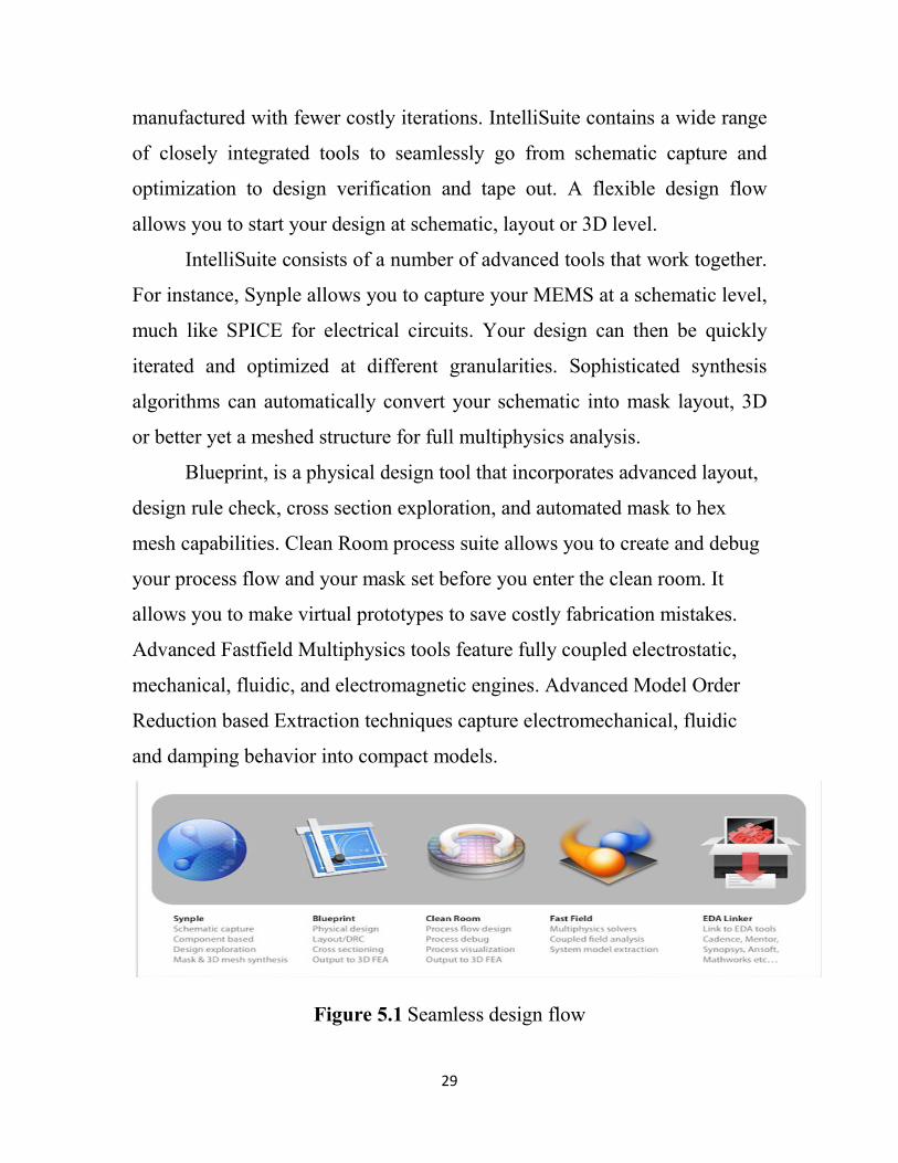
manufactured with fewer costly iterations. IntelliSuite contains a wide range
of closely integrated tools to seamlessly go from schematic capture and
optimization to design verification and tape out. A flexible design flow
allows you to start your design at schematic, layout or 3D level.
IntelliSuite consists of a number of advanced tools that work together.
For instance, Synple allows you to capture your MEMS at a schematic level,
much like SPICE for electrical circuits. Your design can then be quickly
iterated and optimized at different granularities. Sophisticated synthesis
algorithms can automatically convert your schematic into mask layout, 3D
or better yet a meshed structure for full multiphysics analysis.
Blueprint, is a physical design tool that incorporates advanced layout,
design rule check, cross section exploration, and automated mask to hex
mesh capabilities. Clean Room process suite allows you to create and debug
your process flow and your mask set before you enter the clean room. It
allows you to make virtual prototypes to save costly fabrication mistakes.
Advanced Fastfield Multiphysics tools feature fully coupled electrostatic,
mechanical, fluidic, and electromagnetic engines. Advanced Model Order
Reduction based Extraction techniques capture electromechanical, fluidic
and damping behavior into compact models.
Figure 5.1 Seamless design flow

30
5.2 Advantages of intellisuite
The most significant advantage of INTELLISUITE is their major
updates for all software modules and the addition of a new tool, parametric
designer.
Design for manufacturability
1. Fabrication database
2. Thin-film materials engineering
3. Virtual prototyping
Ease of use
1. Consistent user interface
2. Communication with existing tools
Accuracy
1. MEMS-specific meshing and analysis engines
2. In-house code development
3. Validated by in-house MEMS designers
4. ISO certified for quality

31
5.3 Blueprint
Blueprint is the first layout tool designed specifically for the MEMS
community. The goal with Blueprint was to revisit the workflow of the
layout engineer and to create the design that would be effortless to use.
The Blueprint layout editor some new drawing future including an
image import option that let users add JPG, PNG and BMP images into their
current layout. Blueprint is specially designed for constructing and editing
MEMS device masks. It supports layout drawing, VB script layout input,
block hierarchy, design rule check (DRC), and 2D cross-section viewing.
There are five ways to start Blueprint:
Click on IntelliSuite ... Edit Layout in Blueprint from
IntelliFab;
Click on Layout ... Create/Edit ... Top Mask/Bottom Mask from
AnisE;
Click on the Blueprint icon from the Windows Start menu;
Double click on the Blueprint application program;
Double click on any mask file (*.vec, *.gds, *.msk). The .vec,
.gds and .msk are the Blueprint binary file format, industry
standard GDSII file format and InstlliMask text-basedfile.
Figure 5.2 Process in blueprint
32
5.4 Exposure
Exposure is a new addition to IntelliSense’s strong suite of process
simulation tools. This deep resist/SU8 simulator can accurately model
lithography processes like exposure, post-exposure bake, and development.
The dynamic cellular automata simulator and included material databases
ensure robust and speedy lithography simulations.
5.5 Intellifab
IntelliFAB allows designers to takes a different approach. Process
flow forms the basis of creating your devices. This comprehensive process
simulation modules incorporate deposition, etching, bonding, doping,
electroplating, liftoff, and other process steps common in MEMS design.
Other process induced effects, such as micro-assembly, are also addressed to
generate accurate geometric modelsfor the complete range of MEMS
devices.
IntelliFAB, a process simulation module in IntelliSuite, is specially
designed for MEMS process modeling and virtual fabrication. Being a
virtual cleanroom, IntelliFAB offers the capabilities of simulating MEMS
processes that may not be simulated in traditional software packages. With
IntelliFAB, a user can build a process traveller, simulate the process and
visualize the fabricated 3-dimensional structures at the end of each step.
When building a process traveller, the designer uses a standard
process design template and creates a process table on it by selecting such
process steps as wafer or mask definition, thin-film deposition, etching, and
wafer bonding from a database of over 70 process steps. IntelliFAB also

33
features state-of-the-art auto-meshing capabilities to directly mesh solid
models created from the process flow. During the post-fabrication
simulation, a better understanding of the device performance can be
achieved due to incorporation of the processing effects and thin-film
material properties into the device simulation.To open IntelliFAB, select the
following from the start menu of Windows.
Click Start … Programs … IntelliSuite … IntelliFab
Figure 5.3 IntelliFAB main window

34
5.6 Intellietch
The industry’s most powerful wet etch simulator can now simulate
anisotropic etching of quartz in addition to silicon. Features that IntelliEtch
is known for, like etching of high-order planes and multi-masking, are made
easier to use in a huge interface update. The new GPU-based simulator can
run etch simulations over 100 times faster than the previous CPU-based
version.
5.7 3D Builder/hexpresso
IntelliSuite’s state-of-the-art automeshing tools are again updated with
cutting-edge advancements. Material properties and boundary conditions
can be automatically applied when a 3D meshed model is generated. New
adaptive meshing and mesh refinement settings allow users to have full
control over the automated meshing process. Meshing is now faster and
more robust than ever before.
Figure 5.4 Layout of 3D builder
35
5.8 Thermo electro mechanical analysis module
The original MEMS multiphysics simulator has received some powerful
updates in IntelliSuite v8.7. New coupled package-device simulation
capability can be used to analyze packaging effects on a MEMS device.
Dynamic contact analysis can be used to simulate models with multiple
points of contact. IntelliSuite’s powerful reduced-order macromodel
extractor can now generate piezoelectric as well as multi-contact
macromodels. In addition, the finite element solver has been updated to
ensure greater stability and simulation accuracy. It Create Finite Element
Models from masks layouts and process flows, or directlyelement by
element using interactive builder.It includes properties like Piezoelectric
Analysis (Contact, Magnetic, Electromagnetic), Parametric variations and
Sub modeling analysis, Mechanical Deformation with a time varying
voltage signal, Micro assembly and latching modeling.Some of the many
other new features in IntelliSuite v8.7 include:
New MEMS-specific drawing capabilities in the Blueprint™ layout
editor
A new Job Manager™ utility which allows users to queue and run
multiple simulations in a row
New library elements to make design exploration and optimization
easier in the SYNPLE™ schematic-based simulator
A new Mesh Manipulator™ utility which can create curved mesh
surfaces and import/export a variety of file formats.
Independent electrostatic and mechanical meshing based on exposed
face mesh algorithm and support multi-bank exposed face meshing.

36
5.9 Intellimask
IntelliMask is specially designed for constructing and editing MEMS
device level masks. IntelliMask incorporates MEMS specific design features
unavailable in standard electronics and mechanical layout tools.
The tools in IntelliMask are Arcs, Splines, Wires and Curves which
are termed as Standard features. There are five ways to start IntelliMask:
Selecting Construct…Layout…Create Mask from IntelliFab.
Selecting a Create/Edit menu item in the AnisE main user
interface.
Selecting the IntelliMask icon from the Windows Start menu.
Double clicking on the IntelliMask application, or double clicking
on any mask file (“*.msk”).
Figure 5.4 IntelliMask main window
37
CHAPTER-6
MODELING INSTRUCTION
6.1 Steps to design gas sensor
1. Definition Si.
2. Deposition SiO2.
3. Deposition PRS1800.
4. Definition UV.
5. Partially etch photoresist.
6. Partially etch SiO2.
7. Partially etch photoresist.
8. Deposition Si3N4.
9. Deposition photoresist.
10. Definition UV.
11. Etch through photoresist.
12. Etch through Si3N4.
13. Partially etch photoresist.
14. Deposition Au.
15. Deposition ZnO.
16. Deposition photoresist.
17. Definition UV.
18. Etch through photoresist.
19. Etch through ZnO.
20. Partially etch photoresist.
21. Etch Si3N4.
22. Deposition Ti.

38
6.2 Process flow
1. Open the gas sensor process file (ProcessFlow.fab) in IntelliFAB
using the default process database. This can be done by following the steps
below.
2. Launch IntelliFAB.
Click Start …Programs …IntelliSuite …IntelliFab.
3. Click File … Open fab file.
Figure 6.1 Setup window
Click OK.

39
6.3 Fabrication steps
Figure 6.2 The process flow steps in IntelliFAB
The user can explore the process table by double clicking on each of the
process steps and looking at the process parameters.

40
4. Launch FABViewer and visualize the process.
Click Visualize.
Figure 6.3 Definition of silicon
Figure 6.4 Deposition of photoresist
41
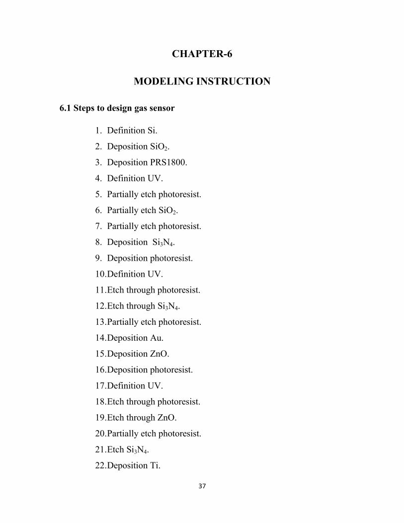
Figure 6.5 Exposure of UV
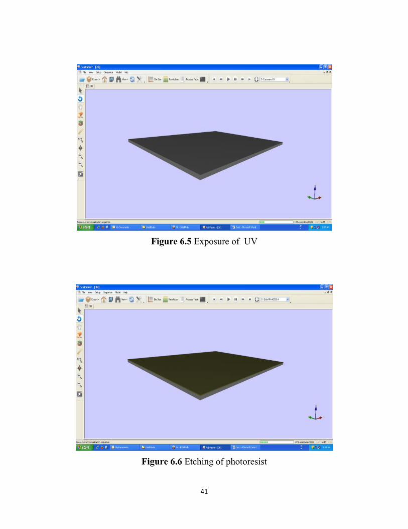
Figure 6.6 Etching of photoresist

42
Figure 6.7 Deposition of Si3N4
Figure 6.8 Deposition of ZnO

43
Figure 6.9 Deposition photoresist
figure 6.10 Deposition of titanium

44
6.4 Thermo-electro-mechanical (TEM) analysis
6.4.1 Export to TEM
1. Click IntelliSuite … TEM.
Figure 6.11 Hexpresso mesh methods
2. Click Mesh Structure.
3. Save the .save file.
Click Save.
Figure 6.12 Mesh parameters

45
4. Click Mesh.
Figure 6.13 Meshing progress
When the meshing is complete, IntelliSuite will automatically create a finite
element model and open it in TEM (Figure 6.14).
Figure 6.14 3D FEA model in TEM

46
6.4.2 View settings
TEM allows the user to independently set the X, Y and Z zoom
factors.
1.The user can use the mouse to move the device in the 3D
space.
2. The user can use the View … Zoom … Define to specify the
view settings in the X, Y and Z directions.
6.4.3 Mesh refinement
1. If the current mesh size is too big, the user can refine the mesh.
Click Mesh … Auto.
2. Enter the maximum mesh size in the dialog box.
IntelliSuite allows the user to apply a variety of loads to the
device. This ranges from force, pressure, Coriolis force, temperature
and other loads. The loads can be constant, time varying or frequency
varying.
3.Start simulation
Click Analysis … Start Static Analysis.
4.View results
Click Result …Displacement…Norm.

47
CHAPTER-7
COMPONENT DESCRIPTION
7.1 Elements of gas sensor
7.1.1 Nafion
Nafion is a sulfonated tetrafluoroethylene based fluoropolymer-
copolymer discovered in the late 1960s by Walther Grot of DuPont. It is the
first of a class of synthetic polymers with ionic properties which are called
ionomers.
7.1.1.1 Preparation
Nafion derivatives are first synthesized by the copolymerization of
tetrafluoroethylene (TFE) and perfluoro (alkyl vinyl ether) with sulfonyl
acid fluoride. The latter reagent can be prepared by the pyrolysis of its
respective oxide or carboxylic acid to give the olefinated structure.
The resulting product is an -SO2F-containing thermoplastic that is
extruded into films. Hot aqueous NaOH converts these sulfonyl fluoride (-
SO2F) groups into sulfonate groups (-SO3−Na+). This form of Nafion,
referred to as the neutral or salt form, is finally converted to the acid form
containing the sulfonic acid (-SO3H) groups. Nafion can be cast into thin
films by heating in aqueous alcohol at 250 °C in an autoclave. By this
process, Nafion can be used to generate composite films, coat electrodes, or
repair damaged membranes.

48
7.1.1.2 Properties
It is highly conductive to cations.
It resists chemical attack. According to DuPont and alkali metals.
The Teflon backbone interlaced with the ionic sulfonate groups gives
Nafion a high operating temperature.
It is selectively and highly permeable to water.
7.1.1.3 Applications
Nafion's superior properties make it suitable for a broad range of
applications. Nafion has found use in fuel cells, electrochemical devices,
chlor-alkali production, metal-ion recovery, water electrolysis, plating,
surface treatment of metals, batteries, sensors, Donnan dialysis cells, drug
release, gas drying or humidifaction, and superacid catalysis for the
production of fine chemicals. It is also often cited for theoretical potential
(i.e., thus far untested) in a number of fields. With consideration of Nafion's
wide functionality, only the most significant will be discussed below.
7.1.1.4 Chlor-alkali production cell membrane
Chlorine and sodium/potassium hydroxide are among the most
produced commodity chemicals in the world. Modern production methods
produce Cl2 and NaOH/KOH from the electrolysis of brine using a Nafion
membrane between half-cells. Before the use of Nafion, industries used
mercury containing sodium amalgam to separate sodium metal from cells or
asbestos diaphragms to allow for transfer of sodium ions between half cells;
both technologies were developed in the latter half of the 19th century. The
disadvantages of these systems is worker safety and environmental concerns

associated with mercury and asbesto
played a part. Nafion was the direct result of the chlor
addressing these concerns; Nafion could tolerate the high temperatures, high
electrical currents, and corrosive environment of the electrolytic cel
Figure 7.1
The figure to the right shows a chlor
functions as a membrane between half cells. The membrane allows sodium
ions to transfer from one cell to the other with minimal electrical resistance.
The membrane was also reinforced with additional membranes to prevent
gas product mixing and minimize back transfer of Cl
side positive and cathode side negative terminal is applied.
7.1.1.5 Proton exchange membrane (PEM) for fuel cells
Although fuel cells have been used since the 1960s as power supplies
for satellites, recently they have received renewed attention for their
potential to efficiently produce clean energy from hydrogen. Nafion was
found effective as a membrane for
cells by permitting hydrogen ion transport while preventing electron
49
associated with mercury and asbestos, although economical factors also
played a part. Nafion was the direct result of the chlor-alkali industry
addressing these concerns; Nafion could tolerate the high temperatures, high
electrical currents, and corrosive environment of the electrolytic cel
Figure 7.1 A chlor-alkali cell
The figure to the right shows a chlor-alkali cell where Nafion
functions as a membrane between half cells. The membrane allows sodium
ions to transfer from one cell to the other with minimal electrical resistance.
membrane was also reinforced with additional membranes to prevent
gas product mixing and minimize back transfer of Cl− and −OH ions. Anode
side positive and cathode side negative terminal is applied.
roton exchange membrane (PEM) for fuel cells
though fuel cells have been used since the 1960s as power supplies
for satellites, recently they have received renewed attention for their
potential to efficiently produce clean energy from hydrogen. Nafion was
found effective as a membrane for proton exchange membrane (PEM)
by permitting hydrogen ion transport while preventing electron
s, although economical factors also
alkali industry
addressing these concerns; Nafion could tolerate the high temperatures, high
electrical currents, and corrosive environment of the electrolytic cells.
alkali cell where Nafion
functions as a membrane between half cells. The membrane allows sodium
ions to transfer from one cell to the other with minimal electrical resistance.
membrane was also reinforced with additional membranes to prevent
OH ions. Anode
though fuel cells have been used since the 1960s as power supplies
for satellites, recently they have received renewed attention for their
potential to efficiently produce clean energy from hydrogen. Nafion was
(PEM) fuel
by permitting hydrogen ion transport while preventing electron
50
conduction. Solid Polymer Electrolytes, which are made by connecting or
depositing electrodes (usually noble metal) to both sides of the membrane,
conduct the electrons through an energy requiring process and rejoin the
hydrogen ions to react with oxygen and produce water. Fuel cells are
expected to find strong use in the transportation industry.
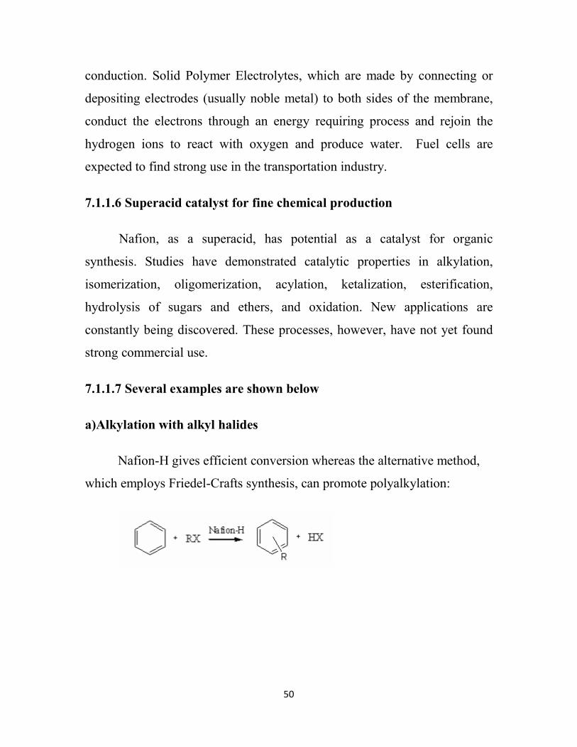
7.1.1.6 Superacid catalyst for fine chemical production
Nafion, as a superacid, has potential as a catalyst for organic
synthesis. Studies have demonstrated catalytic properties in alkylation,
isomerization, oligomerization, acylation, ketalization, esterification,
hydrolysis of sugars and ethers, and oxidation. New applications are
constantly being discovered. These processes, however, have not yet found
strong commercial use.
7.1.1.7 Several examples are shown below
a)Alkylation with alkyl halides
Nafion-H gives efficient conversion whereas the alternative method,
which employs Friedel-Crafts synthesis, can promote polyalkylation:

b)Acylation
The amount of Nafion
with aroyl chloride is 10–
c)Catalysis
Nafion-H increases
o-trialkylsilation of alcohols, phenol, and carboxy
d)Isomerization
Nafion can catalyze a
enzymes within the Nafion by enlarging pores with
maintains a structure and pH to provide a stable environment for the
enzymes.
Applications include catalytic oxid
51
The amount of Nafion-H needed to catalyze the acylation of benzene
–30% less than the Friedel-Crafts catalyst:
H increases reaction rates of protection via dihydropyran or
trialkylsilation of alcohols, phenol, and carboxylic acids.
Nafion can catalyze a 1,2-hydride shift. It is possible to immobilize
within the Nafion by enlarging pores with lipophilic salts. It
maintains a structure and pH to provide a stable environment for the
Applications include catalytic oxidation of adenine dinucleotides.
H needed to catalyze the acylation of benzene
Crafts catalyst:
via dihydropyran or
. It is possible to immobilize
salts. It
maintains a structure and pH to provide a stable environment for the
.
52
7.1.1.8 Sensors
Nafion has found use in the production of sensors, which with
application in ion-selective, metallized, optical, and biosensors. What makes
Nafion especially interesting is its demonstration in biocompatibility. It has
been shown to be stable in cell cultures as well as the human body, and there
is considerable research towards the production of higher sensitivity glucose
sensors.
7.1.1.9 Modified nafion for PEM fuel cells
Normal Nafion will dehydrate (thus lose proton conductivity) when
temperature is above ~80 °C. This limitation troubles the design of fuel
cells, because higher temperatures are desirable for a better efficiency and
CO tolerance of the platinum catalyst. Silica and zirconium phosphate can
be incorporated into Nafion water channels through in situ chemical
reactions to increase the working temperature to above 100 °C.

53
7.1.2 Platinum
Platinum black is widely used as a thin film covering solid platinum
metal, forming platinum electrodes for applications in electrochemistry. The
process of covering platinum electrodes with such a layer of platinum black
is called "platinization of platinum". The platinized platinum has a true
surface area much higher than the geometrical surface area of the electrode
and, therefore, exhibits action superior to that of shiny platinum.
Platinum black powder is used as a catalyst in proton exchange
membrane fuel cells. In common practice, the platinum black is either
sprayed using an ultrasonic nozzle or hot pressed onto the membrane or gas
diffusion layer. A suspension of platinum black and carbon powder in
ethanol-water solutions serves to optimize the uniformity of the coating,
electrical conductivity, and in the case of application to the membrane, to
prevent dehydration of the membrane during the application. Historically
many "self-lighting" gas lamps, ovens, and stove burners used platinum
black to catalyze the oxidation of a small amount of gas, lighting the device
without a match or spark. This works particularly well for producer gas,
town gas, and wood gas which contain a substantial fraction of hydrogen gas
(H2) which is particularly well catalyzed by platinum black.
Platinum black powder can be manufactured from ammonium
chloroplatinate by heating at 500 °C in molten sodium nitrate for 30
minutes, followed by pouring the melt into water, boiling, washing, and
reduction of the brown powder (believed to be platinum dioxide) with
gaseous hydrogen to platinum black. Before platinization, the platinum
surface is cleaned by immersion in aqua regia (50% solution, i.e., 3 volumes

54
of 12 mol/kg of HCl, 1 volume of 16 mol/kg HNO3, 4 volumes of water).
Platinization is often conducted from water solution of 0.072 mol/kg of
chloroplatinic acid and 0.00013 mol/kg of lead acetate, at a current density
of 30 mA/cm2 for up to 10 minutes. The process evolves chlorine at the
anode; the interaction of the chlorine with the cathode is prevented by
employing a suitable separation (e.g. a glass frit). Electroplating with the
current density of 5 mA/cm2 while reversing the polarity. After platinization,
the electrode should be rinsed and stored in distilled water. The electrode
loses its catalytic properties on prolonged exposure to air. Platinum sponge
is yet another form of platinum metal with a developed surface area, distinct
from platinum black and platinized platinum. Platinum sponge can be
obtained by strongly heating ammonium chloroplatinate. It has a gray to
black colour, while its catalytic properties vary depending on the specifics of
the manufacturing. Hydrogen saturated hydrochloric acid, the shiny
platinum electrode is observed to assume positive potential versus that of
platinum black at zero net current (+ 340 mV at room temperature). With the
temperature increasing to 70 °C, the difference in potentials dropped to zero.
The reason for this is not perfectly clear, although several explanations have
been proposed.
7.1.2.1 Choice of platinum
Inertness of platinum (it does not corrode).
The capability of platinum to catalyze the reaction of proton
reduction.
A high intrinsic exchange current density for proton reduction on
platinum.
Excellent reproducibility of the potential.
55
a)The surface of platinum is platinized to the following reasons
Increase total surface area. This improves reaction kinetics and
maximum possible current.
Use a surface material that adsorbs hydrogen well at its interface. This
also improves reaction kinetics.
Other metals can be used for building electrodes with a similar function such
as the palladium-hydrogen electrode. Because of the high adsorption activity
of the platinized platinum electrode, it's very important to protect electrode
surface and solution from the presence of organic substances as well as from
atmospheric oxygen. Inorganic ions that can reduce to a lower valency state
at the electrode also have to be avoided (e.g., Fe3+, CrO42−). A number of
organic substances are also reduced by hydrogen at a platinum surface, and
these also have to be avoided.
b)Cations that can reduce and deposit on the platinum can be source of
interference
silver, mercury, copper, lead, cadmium and thallium.
Substances that can inactivate ("poison") the catalytic sites include arsenic,
sulfides and other sulfur compounds, colloidal substances, alkaloids, and
material found in living systems.

56
7.1.3 Micro-hotplate
The concept of micro-hotplates on silicon appeared in the 80’s and
was first used for thermal and gas sensors. Micro-hotplates have been used
in gas sensors, integrated circuits, actuators and fluidics systems in fields
such as electronic noses, electronics, space, biomedical and micro total
analysis systems.
Depending on the applications, different fabrication techniques were
used to thermally isolate the heating element. The first versions were used
for polymer and metal-oxide gas sensors. Lately, micro-hotplates for drop-
coated and MOSFET gas sensors were designed. The processing of the
micro-hotplates having a silicon island was modified to thermally isolate
electronic devices. An array of 4 gas sensitive MOSFETs including a diode
used as temperature sensor and a heating resistor were implemented in the
silicon island suspended by a dielectric membrane.
The MOSFET have their gate replaced by catalytic metals and are
suitable for gas sensing operation at an operating temperature up to 200°C.
The low-thermal mass device allows new modes of operation for MOSFET
gas sensors such as a cycled temperature mode and combined field-effect
and the next generation of low-power MOSFET will be fabricated using
Silicon On Insulator (SOI) wafers to decrease the mass of the silicon island
in the aim of improving the power consumption and the thermal time
constant of the device.
Micro-hotplates are integrated in the system to lower the power
consumption and thermal constant time. Micro-hotplates can be used for
instance in micro-thruster for the control of nano satellites. They have been
also developed for chemical micro sensors for space application. Another

57
area of application is in the “lab on chip” systems for micro total analysis. At
IMT, the work on micro-hotplates has started on gas sensing applications.
The micro-hotplates are also of interest for pneumatic actuator
systems. Micro-transportation systems applicable to highly clean
environment are in great demand, and the practicability of pneumatic
conveyor suitable to IC-process and micro factory has previously been
demonstrated. Pneumatics actuators are spared from the problem of particle-
attraction and the version developed at IMT is valve free. They have shown
excellent switching behavior of the working gas by thermo-electrically-
triggered Coanda effect. Since many nozzles are used to move the slider in
the conveyor, micro-hotplates are integrated in the system to lower the
power consumption and thermal constant time.
In this communication, a review of the micro-hotplates design and
processing developed mainly at IMT will be presented for these different
applications.Micro-hotplates from IMT are based on a low stressPECVD or
LPCVD silicon nitride membrane. In the case of metal-oxide gas sensors,
the heater and the electrodes are made of platinum. The insulator between
them can be composed of silicon nitride or oxide thin films. The micro-
hotplates withstand a high annealing temperature of 700°C necessary for
drop-coated gas sensors. They can also be operated in a pulsed temperature
mode of operation to temperatures up to 700°C. This makes possible the
annealing on chip of the gas sensitive coating. A silicon island was added
underneath the membrane to improve the temperature distribution over the
sensing area.
Finally, upcoming activities on space and micro total analysis systems
will be presented. Micro-hotplates can be used for instance in micro-thruster
for the control of nanosatellites. They have been also developed for chemical

58
microsensors for space applications. Another area of application is in the
“lab on chip” systems for micro total analysis. Flow sensors and heaters are
needed to control the chemical reactions such as in Polymerase Chain
Reaction (PCR) where the temperature has to be cycled.
59
CHAPTER-8
RESULT AND DISCUSSION
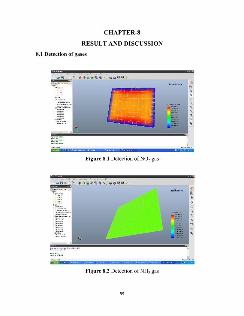
8.1 Detection of gases
Figure 8.1 Detection of NO2 gas
Figure 8.2 Detection of NH3 gas

60
Figure 8.3 Detection of SO2 gas
Figure 8.4 Detection of CO2 gas
61
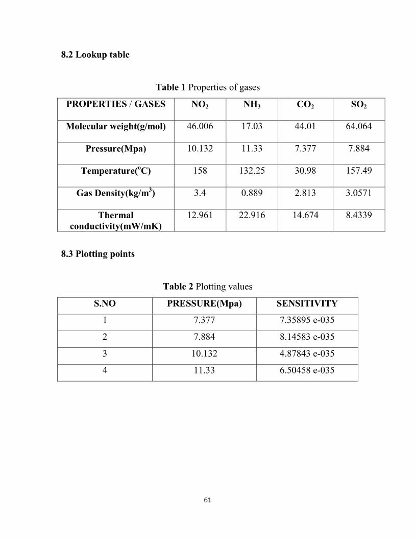
8.2 Lookup table
Table 1 Properties of gases
PROPERTIES / GASES
NO2 NH3 CO2 SO2
Molecular weight(g/mol)
46.006 17.03 44.01 64.064
Pressure(Mpa)
10.132 11.33 7.377 7.884
Temperature(oC)
158 132.25 30.98 157.49
Gas Density(kg/m3)
3.4 0.889 2.813 3.0571
Thermal conductivity(mW/mK)
12.961 22.916 14.674 8.4339
8.3 Plotting points
Table 2 Plotting values
S.NO PRESSURE(Mpa) SENSITIVITY
1 7.377 7.35895 e-035
2 7.884 8.14583 e-035
3 10.132 4.87843 e-035
4 11.33 6.50458 e-035

62
8.3 Sensitivity plot
Figure 8.5 Pressure Vs Sensitivity
0
0.01
0.02
0.03
0.04
0.05
0.06
7.3 7.8 10 11
Sen
siti
vity
Sensitivity Plot
Pressure(Mpa)

63
CHAPTER-9
CONCLUSION & FUTURE WORK
9.1 Conclusion
The MEMS gas sensor using CNT-FET array is presented has high
sensitivity, selectivity, fast response and recovery time. This sensor is used
as a point of care testing in asthma diagnosis. The design and fabrication of
suitable CNT-FET array, the stability and sensor response during long
period of time, humidity, etc. can be improved. Once this technology gets
commercialized it will be broadly implemented. Due to the enormous
application, it might be reasonable to hope that the large scale fabrication
method of CNT-FET would be developed resulting in the decrease of the
cost.
9.2 Future work
Future work will continue to focus on generating improved
component assembly and device fabrication strategies. For small or medium-
scale batch production, a hybrid design whereby component parts are created
separately for subsequent assembly into a complete system is an attractive
option, as it removes many of the restrictions imposed by the need for
process compatibility. Integrated gas sensor with a micro-hotplate (MHP)
demonstrates better sensitivity, faster response, and lower power
consumption than traditional thick film devices. For the detection of a target
gas, a gas-sensitive layer is applied on a suspended micro-hotplate that is
mounted on top of a silicon chip. Any gas-induced change of the gas-
sensitive layer’s surface potential is detected and digitally processed by the
integrated electronics.

64
CHAPTER-10
REFERENCES
1. A.Afzal, et al, (2012) “NOx sensor based on semiconducting metal
oxide nanostructures” Sensors and Actuators B 171– 172, 25– 42.
2. B. Gao, Y.F. Chen, M.S. Fuhrer, D.C. Glattli, A. Bachtold, (2005)
“Four-point resistance of individual single-wall carbon nanotubes”,
Phys. Rev. Lett. 95, 196802.
3. Charles P. Poole Jr , Frank J. Owens, (2012) “Introduction to
nanotechnology”, Wiley India Pvt.Ltd.
4. E.N.Ganesh, (March 2013) “International Journal of Innovative
Technology And Exploring Engineering (IJITEE)” ISSN: 2278-3075,
volume-2, issue-4,.
5. E.S. Snow, F.K. Perkins, (2005) “Capacitance and conductance of
single-walled carbon nano tubes in the presence of chemical vapors”,
Nano Lett. 5 (12).
6. F. Wakaya, T. Nagai, and K. Gamo, (2002) “Position control of
carbon nano tube using patterned electrode and electric field”
Microelectronic Engineering, vol. 63, no. 1–3, pp. 27–31.
7. F.Opekar, K.Stulik, (1999) “Electrochemical sensors with solid
polymer electrolytes”, Anal. Chim. Acta, 385, 151.
8. Hithesh K Gatty, S. Leijonmarck, M. Antelius1, G. Stemme and N.
Roxhed, (2014 )“Miniaturized amperometric NO sensor”, Phys. Rev.
Lett. 95, 196802.
65
9. J. Li, (2012) “Carbon nanotubes applications: chemical and physical
sensors”, in Carbon Nanotubes: Science and Applications, M.
Meyyappan, Ed., CRC Press, Boca Raton, Fla, USA.
10. J. Li, Y. Lu, Q. Ye, et al., (2003) “Carbon nano tubes sensors for gas
and organic vapour detection,” Nano Letters, vol. 3, no. 7, pp. 929–
933.
11. M. Glykas and P. Chytas, (2004) “Technological innovations in
asthma patient monitoring and care,” Expert Systems with
Applications, vol. 27, no. 1,pp. 121 – 131.
12. M.J. Yaceman, M.M.Yoshida, Rendson. J, G.Santiestaban (1993)
“Catalytic growth of carbon micro tubules with fullerneess structure”
Applied physics letter colume – 62, pp 202 –204.
13. Morinubo Endo, Sumio Lijima, MildredS.Dresselhaus, (2011)
“Introductionto carbon nanotubes” IEEE Transactions on Electron
Devices, VOL 54,No.6.
14. N. Sinha, J. Ma, J.T.W. Yeow, (2006) “Carbon nanotube-based
sensors”, J. Nanosci. Nanotechnol. 6 573–590.
15. Occhiuzzi et al, (October 2011) “RFID Passive Gas Sensor
Integrating Carbon Nanotubes”, IEEE Transactions on Microwave
Theory and Techniques, VOL.59, NO.10.
16. P. Na, H. Kim, H.M. So, K.J. Kong, H. Chang, B. Ryu, Y. Choi, J.O.
Lee, B.K. Kim, J.J.Kim, J. Kim, (2005) “Investigation of the
humidity effect on the electrical properties of single-walled carbon
nano tube transistors”, Appl. Phys. Lett. 87, 093101.
17. P.Bondavalli, L.Gorintin, P. Legagneux, (2014) “Selective gas
detection using air brush technique” ISSN: 2277-3878, Volume-1,
Issue-4.

66
18. R.S. Ruoff, D. Qian, W. Kam Liu, (2003) “ Mechanical properties of
carbon nanotubes: theoretical predictions and experimental
measurements”, C. R. Phys. 4, 993–1008.
19. S. Ijima and T. Ichihashi, (1992) “Single cell carbon nano tube of 1
nanometer diameter” Nature Volume 363, pp –220 – 221.
20. T.R. Han, V. Joshi, J.C.P. Gabriel, G. Grüner, (2004)
“Nanoelectronic carbon dioxide sensors”, Adv. Mater. 16, 2049–2052.
21. Yun Wang and John T.W.Yeow, (2009) “A Review of carbon nano
tubes based sensor”, IEEE Transactions on Electron Devices, VOL
54,No.6.

67