DNA/STP-AO-250 0-35VDC, 250 mA Current Buffer Board User ...
15
i DNA/STP-AO-250 0-35VDC, 250 mA Current Buffer Board — User Manual Version 1.0 February 2011 Edition PN Man-DNA-STP-AO250-0211 © Copyright 2011 United Electronic Industries, Inc. All rights reserved.
Transcript of DNA/STP-AO-250 0-35VDC, 250 mA Current Buffer Board User ...

DNA/STP-AO-2500-35VDC, 250 mA
Current Buffer Board—
User Manual
Version 1.0February 2011 Edition
PN Man-DNA-STP-AO250-0211
© Copyright 2011 United Electronic Industries, Inc. All rights reserved.
i
DNA-STP-AO-250 User Manual
No part of this publication may be reproduced, stored in a retrieval system, or transmitted, in any form by any means, electronic, mechanical, by photocopying, recording, or otherwise without prior written permission.
Information furnished in this manual is believed to be accurate and reliable. However, no responsibility is assumed for its use, or for any infringement of patents or other rights of third parties that may result from its use.
All product names listed are trademarks or trade names of their respective companies.
See the UEI website for complete terms and conditions of sale:
http://www.ueidaq.com/company/terms.aspx
Contacting United Electronic Industries
Mailing Address:
27 Renmar AvenueWalpole, MA 02081U.S.A.
For a list of our distributors and partners in the US and around the world, please see http://www.ueidaq.com/partners/
Support:
Telephone: (508) 921-4600Fax: (508) 668-2350
Also see the FAQs and online “Live Help” feature on our web site.
Internet Support:
Support: [email protected]: www.ueidaq.comFTP Site: ftp://ftp.ueidaq.com
Product Disclaimer:
WARNING!
DO NOT USE PRODUCTS SOLD BY UNITED ELECTRONIC INDUSTRIES, INC. AS CRITICAL COMPONENTS IN LIFE SUPPORT DEVICES OR SYSTEMS.
Products sold by United Electronic Industries, Inc. are not authorized for use as critical components in life support devices or systems. A critical component is any component of a life support device or system whose failure to perform can be reasonably expected to cause the failure of the life support device or system, or to affect its safety or effectiveness. Any attempt to purchase any United Electronic Industries, Inc. product for that purpose is null and void and United Electronics Industries, Inc. accepts no liability whatsoever in contract, tort, or otherwise whether or not resulting from our or our employees' negligence or failure to detect an improper purchase.
Specifications listed in this document are subject to change without notice. Please check with UEI for current status.
ii
iii
Tel:508-921-4600 www.ueidaq.com Vers: 1.0Date: February 2011 DNA-STP-AO-250-
© Copyright 2011United Electronic Industries, Inc.
Table of Contents
Chapter 1 Introduction . . . . . . . . . . . . . . . . . . . . . . . . . . . . . . . . . . . . . . . . . . . . . . . . . . . . 1
1.1 Organization of this Manual . . . . . . . . . . . . . . . . . . . . . . . . . . . . . . . . . . . . . . . . . . . . 1
1.2 The DNA-STP-AO-250 Board. . . . . . . . . . . . . . . . . . . . . . . . . . . . . . . . . . . . . . . . . . . 21.2.1 Features. . . . . . . . . . . . . . . . . . . . . . . . . . . . . . . . . . . . . . . . . . . . . . . . . . . . . . 21.3.2 Use of Two STP-AO-250 Boards with one Host AO-308. . . . . . . . . . . . . . . . . 4
1.4 Pinout Diagrams . . . . . . . . . . . . . . . . . . . . . . . . . . . . . . . . . . . . . . . . . . . . . . . . . . . . . 5
1.5 Device Architecture. . . . . . . . . . . . . . . . . . . . . . . . . . . . . . . . . . . . . . . . . . . . . . . . . . . 9
Appendix A — Accessories . . . . . . . . . . . . . . . . . . . . . . . . . . . . . . . . . . . . . . . . . . . . . . . . . 10
Index . . . . . . . . . . . . . . . . . . . . . . . . . . . . . . . . . . . . . . . . . . . . . . . . . . . . . . . . . . . . . . . . . . 11
iv
Tel::508-921-4600 www.ueidaq.com Vers: 1.0Date: February 2011 DNA-STP-AO-250-ManualLOF.fm
© Copyright 2011United Electronic Industries, Inc.
List of FiguresChapter 1 Introduction . . . . . . . . . . . . . . . . . . . . . . . . . . . . . . . . . . . . . . . . . . . . . . . . . . . . . . 11-1 Photo of STP-AO-250 Current Buffer Board.................................................................. 21-2 STP-AO-250 Product Features...................................................................................... 21-3 Accuracy Curves ........................................................................................................... 31-4 Interconnection Diagram for Two STP-AO-250 Current Buffer Boards (Master/Slave). 41-5 STP-AO-250 Technical Specifications........................................................................... 51-6 Pinout of DB-37 Input Connector ................................................................................... 51-7 Pinout of DB-37 Output Connector ................................................................................ 61-8 Pinout of STP-AO-250 Calibration Connector ............................................................... 71-9 Pinout of STP-AO-250 TB1 Screw Terminal Board ....................................................... 81-10 Output Circuit of DNA-STP-AO-250 Current Buffer Board ............................................ 9
Appendix A — Accessories . . . . . . . . . . . . . . . . . . . . . . . . . . . . . . . . . . . . . . . . . . . . . . . . . 10A-1 Photo of DNA/DNR-CBL-62 Flat Ribbon Accessory Cable ......................................... 10A-2 Photo of DNA/DNR CBL-37S Round, Shielded Accessory Cable ............................... 10

DNA-STP-AO-250 Current Buffer BoardChapter 1 1
Introduction
Chapter 1 Introduction
This document outlines the feature set and use of the DNA-STP-AO-250 Current Buffer Board.
1.1 Organization of this Manual
This DNA-STP-AO-250 User Manual is organized as follows:
• IntroductionProvides an overview of DNA-STP-AO-250 High Current OutputBuffer Board list of features, technical specifications, and accessories.This product is designed for use with UEI DNx-AO-308 series analogoutput boards.
• Appendix A: AccessoriesThis appendix provides a list of accessories available for DNA-STP-AO-250 current buffer boards.
• IndexThis is an alphabetical listing of the topics covered in this manual.
ConventionsTo help you get the most out of this manual and our products, please note that we use the following conventions:
Tips are designed to highlight quick ways to get the job done, orreveal good ideas you might not discover on your own.
NOTE: Notes alert you to important information.
CAUTION! Caution advises you of precautions to take to avoid injury,data loss, and damage to your boards or a system crash.
Text formatted in bold typeface generally represents text that should be entered verbatim. For instance, it can represent a command, as in the following example: “You can instruct users how to run setup using a command such as setup.exe.”
Tel: 508-921-4600 www.ueidaq.com Vers: 1.0Date: February 2011 File: STP-AO-250-Chap1.fm
© Copyright 2011 all rights reservedUnited Electronic Industries, Inc.

DNA-STP-AO-250 Current Buffer BoardChapter 1 2
Introduction
1.2 The DNA-STP-AO-250 Board
A photo of the DNA-STP-AO-250 high current buffer board is shown in Figure 1-1 below.
Figure 1-1. Photo of STP-AO-250 Current Buffer Board
Note also that the top of DNA-STP-AO-250 board, although not physically covered, has no active signals exposed except those on the various connectors and screw terminals.
1.2.1 Features The STP-AO-250 high current buffer board has the following features:
Figure 1-2. DNA-STP-AO-250 Product Features
Inputs from AO-308(Ch 0 to Ch 7)
Outputs to second STP-AO-250 board (Ch 4 to 7)
Screw Terminal Blockfor connections to loads and DIO.
Alternate Connector for
Power In
loads and DIO
Sense Line On/Offswitches (4)
DC/DCConverters
JVCC1JVCC2 andJL4 (notpopulated)
FAN with snap-on grid/filter.(Clean periodically.)
JPOWER1(Not used)
DNA-STP-AO-2500- 35 VDC, 250 mA Current Buffer Board
250 mA per channel, continuous
0-35 VDC Volt output, minimum
Tel: 508-921-4600 www.ueidaq.com Vers: 1.0Date: February 2011 File: STP-AO-250-Chap1.fm
© Copyright 2011 all rights reservedUnited Electronic Industries, Inc.

DNA-STP-AO-250 Current Buffer BoardChapter 1 3
Introduction
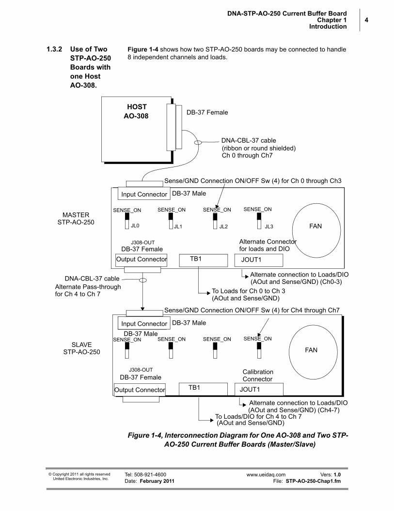
Note that the STP-AO-250 has four independent analog output channels from the host DNx-AO-308 board (Channels 0 to 3). Channels 4 through 7 from the host AO-308 can be passed through one STP-AO-250 to a second STP-AO-250 and then to loads for Channel 4 through 7 as shown in Figure 1-4. Sense/GND line connections can also be made to all loads to improve accuracy. Refer to Figure 1-3 for accuracy curves for various loads and types of connections. Refer to Figure 1-10 for the Output Circuit used to connect the STP-AO-250 to its associated loads.
Figure 1-3. Accuracy Curves for Host AO-308 Output vs. Load
In Figure 1-3 above, note how increasing load resistance reduces error. Also, note that we only use a voltage range of 0 to +10VDC from the AO-308. No negative polarity voltage is used.
Output Voltage Error vs. Voltage vs. Load(±10V output range)
0 5-5-10
10-0.005
0.005
0.015
0.025
0.035
-0.015
-0.025
-0.035
Output Voltage, V
Erro
r, %
2 KOhm load
1 MOhm load
Tel: 508-921-4600 www.ueidaq.com Vers: 1.0Date: February 2011 File: STP-AO-250-Chap1.fm
© Copyright 2011 all rights reservedUnited Electronic Industries, Inc.
DNA-STP-AO-250 Current Buffer BoardChapter 1 4
Introduction
1.3.2 Use of Two STP-AO-250 Boards with one Host AO-308.
Figure 1-4 shows how two STP-AO-250 boards may be connected to handle 8 independent channels and loads.
Figure 1-4, Interconnection Diagram for One AO-308 and Two STP-AO-250 Current Buffer Boards (Master/Slave)
AO-308HOST
To Loads for Ch 0 to Ch 3 Alternate Pass-through
TB1
TB1
JOUT1
JOUT1
DB-37 Male
Alternate Connector for loads and DIO
Output Connector
Input Connector
DB-37 Female
DNA-CBL-37 cable
DNA-CBL-37 cable
Output Connector
Input Connector
DB-37 Male
DB-37 Female
DB-37 Female
(ribbon or round shielded)
SENSE_ON SENSE_ONSENSE_ONSENSE_ON
Sense/GND Connection ON/OFF Sw (4) for Ch 0 through Ch3
DB-37 MaleInput Connector
SENSE_ON SENSE_ONSENSE_ONSENSE_ON
Sense/GND Connection ON/OFF Sw (4) for Ch4 through Ch7
for Ch 4 to Ch 7
FAN
FAN
Calibration Connector
MASTERSTP-AO-250
SLAVESTP-AO-250
To Loads/DIO for Ch 4 to Ch 7
(AOut and Sense/GND)
(AOut and Sense/GND)
Ch 0 through Ch7
JL0 JL1 JL2 JL3
J308-OUT
J308-OUT
Alternate connection to Loads/DIO (AOut and Sense/GND) (Ch0-3)
(AOut and Sense/GND) (Ch4-7)Alternate connection to Loads/DIO
Tel: 508-921-4600 www.ueidaq.com Vers: 1.0Date: February 2011 File: STP-AO-250-Chap1.fm
© Copyright 2011 all rights reservedUnited Electronic Industries, Inc.
DNA-STP-AO-250 Current Buffer BoardChapter 1 5
Introduction
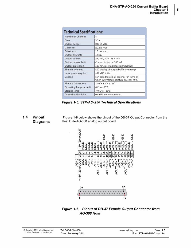
Figure 1-5. STP-AO-250 Technical Specifications
1.4 Pinout Diagrams
Figure 1-6 below shows the pinout of the DB-37 Output Connector from the Host DNx-AO-308 analog output board:
Figure 1-6. Pinout of DB-37 Female Output Connector from AO-308 Host
Technical Specifications:
Gain 3.5 x
0 to 35 VDC
Gain error ±0.2%, max
±3 mV, max
5 V/μS
250 mA, at 0 - 35 V, min
Current limited at 300 mA
Input power required
AG
ND
+15
V (
20m
A)O
UT
DIO
0D
IO1
AG
ND
DN
/C
AO
UT
7 G
ND
AO
UT
6A
GN
DA
OU
T5 G
ND
AO
UT
4A
GN
DA
OU
T3 G
ND
AG
ND
AO
UT
2A
GN
DA
OU
T1 G
ND
AO
UT
0A
GN
D
-15V
(20
mA
)OU
TA
GN
DD
IO2
AG
ND
AG
ND
DN
/CA
OU
T7
AG
ND
AO
UT
6 G
ND
AO
UT
5A
GN
DA
OU
T4
GN
DA
OU
T3
AG
ND
AO
UT
2 G
ND
AO
UT
1A
GN
DA
OU
T0
GN
D
1 2 3 4 5 6 7 8 9 10 11 12 13 14 15 16 17 18 19
1 20 21 22 23 24 25 26 27 28 29 30 31 32 33 34 35 36 37
1 19
20 37
22
Tel: 508-921-4600 www.ueidaq.com Vers: 1.0Date: February 2011 File: STP-AO-250-Chap1.fm
© Copyright 2011 all rights reservedUnited Electronic Industries, Inc.
DNA-STP-AO-250 Current Buffer BoardChapter 1 6
Introduction
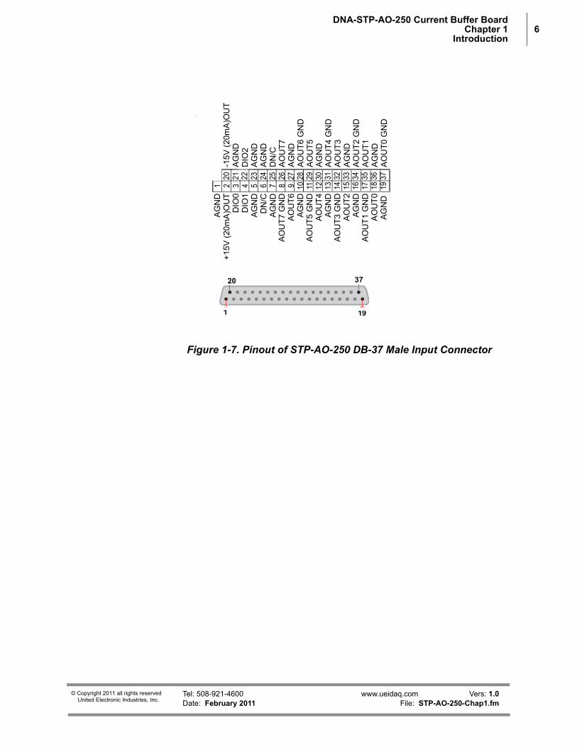
Figure 1-7. Pinout of STP-AO-250 DB-37 Male Input Connector
AG
ND
+1
5V (
20m
A)O
UT
DIO
0D
IO1
AG
ND
DN
/C
AO
UT
7 G
ND
AO
UT
6A
GN
DA
OU
T5 G
ND
AO
UT
4A
GN
DA
OU
T3 G
ND
AG
ND
AO
UT
2A
GN
DA
OU
T1 G
ND
AO
UT
0A
GN
D
-15V
(20m
A)O
UT
AG
ND
DIO
2A
GN
DA
GN
DD
N/C
AO
UT
7A
GN
DA
OU
T6 G
ND
AO
UT
5A
GN
DA
OU
T4 G
ND
AO
UT
3A
GN
DA
OU
T2 G
ND
AO
UT
1A
GN
DA
OU
T0 G
ND
1 2 3 4 5 6 7 8 9 10 11 12 13 14 15 16 17 18 19
1 20 21 22 23 24 25 26 27 28 29 30 31 32 33 34 35 36 37
1 19
20 37
22
Tel: 508-921-4600 www.ueidaq.com Vers: 1.0Date: February 2011 File: STP-AO-250-Chap1.fm
© Copyright 2011 all rights reservedUnited Electronic Industries, Inc.

DNA-STP-AO-250 Current Buffer BoardChapter 1 7
Introduction
below shows the pinout of the DB-37 Output and Alternate Connectors.
Figure 1-8. Pinouts of DB-37 Output Connectors
The figure below shows the pinout of the DB-37 Calibration Connector:
Figure 1-9. Pinout of TB1 Screw Terminal Block
GND 1+15V 2 20 -15V
RSVD 3 21 GND
RSVD 4 22 RSVD
GND 5 23 GND
+VA OUT 6 24 GND
GND 7 25 -VA OUT
RSVD 8 26 RSVD
RSVD 9 27 GND
GND 10 28 RSVD
RSVD 11 29 RSVD
RSVD 12 30 GND
GND 13 31 RSVD
SENSE/GND3 14 32 AOUT3
AOUT2 15 33 GND
GND 16 34 SENSE/GND2
SENSE/GND1 17 35 AOUT1
AOUT0 18 36 GND
GND 19 37 SENSE/GND0
GND 1+15V 2 20 -15V
RSVD 3 21 GND
RSVD 4 22 RSVD
GND 5 23 GND
RSVD 6 24 GND
GND 7 25 RSVD
RSVD 8 26 RSVD
RSVD 9 27 GND
GND 10 28 RSVD
RSVD 11 29 RSVD
RSVD 12 30 GND
GND 13 31 RSVD
GND 14 32 AOUT7
AOUT6 15 33 GND
GND 16 34 GND
GND 17 35 AOUT5
AOUT4 18 36 GND
GND 19 37 GND
JOUT1 High CurrentOutput Connector
J308-OUT connector
19
37 20
1 19
37 20
1
DB-37 (female)37-pin Connector
DB-37 (female)37-pin Connector
JOUT1
JOUT1 Alternate Connector J308-OUT Output Connector
Scre
w T
erm
inal
Con
n
SHIE
LD
1G
ND
2D
IO0
3G
ND
4D
IO1
5G
ND
6D
IO2
7G
ND
8
GN
D
9G
ND
10
GN
D
11SE
NSE
/GN
D0
12A
OU
T0
13SE
NSE
/GN
D1
14A
OU
T1
15SE
NSE
/GN
D2
16A
OU
T217
SEN
SE/G
ND
3 18
AO
UT3
19
GN
D
20
Note: AOUT0 to AOUT3 are forMaster STP-AO-250 CH 0 through Ch3. For Slave STP, theseterminals apply to Ch 4 through Ch7.
Tel: 508-921-4600 www.ueidaq.com Vers: 1.0Date: February 2011 File: STP-AO-250-Chap1.fm
© Copyright 2011 all rights reservedUnited Electronic Industries, Inc.
DNA-STP-AO-250 Current Buffer BoardChapter 1 8
Introduction
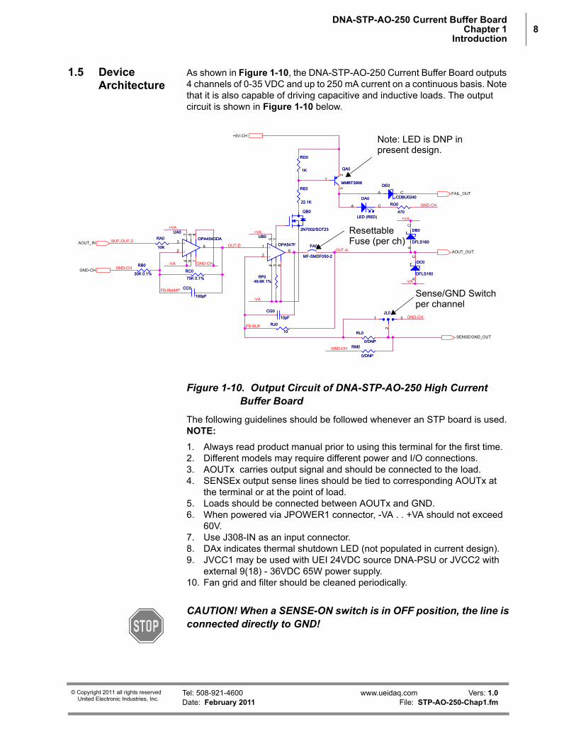
1.5 Device Architecture
As shown in Figure 1-10, the DNA-STP-AO-250 Current Buffer Board outputs 4 channels of 0-35 VDC and up to 250 mA current on a continuous basis. Note that it is also capable of driving capacitive and inductive loads. The output circuit is shown in Figure 1-10 below.
Figure 1-10. Output Circuit of DNA-STP-AO-250 High Current Buffer Board
The following guidelines should be followed whenever an STP board is used.NOTE:
1. Always read product manual prior to using this terminal for the first time.2. Different models may require different power and I/O connections.3. AOUTx carries output signal and should be connected to the load.4. SENSEx output sense lines should be tied to corresponding AOUTx at
the terminal or at the point of load.5. Loads should be connected between AOUTx and GND.6. When powered via JPOWER1 connector, -VA . . +VA should not exceed
60V.7. Use J308-IN as an input connector.8. DAx indicates thermal shutdown LED (not populated in current design).9. JVCC1 may be used with UEI 24VDC source DNA-PSU or JVCC2 with
external 9(18) - 36VDC 65W power supply.10. Fan grid and filter should be cleaned periodically.
CAUTION! When a SENSE-ON switch is in OFF position, the line isconnected directly to GND!
���
������
� ��� �� ��
�������
���
��
��� �
����
����
����
��
� ��
����
���
�� ����
����
����
����������� �
�� ��� �
������ �
��
�������
��
�������
�
���
�����
���
�����
�
�
��
�������
�
�
��
��������
�
��
�!�
���
��"
���
��"
���
���
���
���
#��#���
�
�
�
��
���������
�
�
��
����������
�
�� �
� !$
��
��"%�&�'
��
��"%�&�'
���
��"%�&�'
���
��"%�&�'
���
�����
���
�����
���
�"
���
�"
����(�
����(�
���
�� � ��
���
�� � ���
���
���������
���
���������
)��
���� ���� �
)��
���� ���� �
�#�
��
�#�
��
)��
�����$��
)��
�����$��
�
�
���
���%*���+
���
���%*���+
�
���
�������
���
�������
�
���
&�"
���
&�"
����$&$"%�'���
�$&$"%�'
�
���(�
�
���(�
Note: LED is DNP inpresent design.
Sense/GND Switchper channel
ResettableFuse (per ch)
Tel: 508-921-4600 www.ueidaq.com Vers: 1.0Date: February 2011 File: STP-AO-250-Chap1.fm
© Copyright 2011 all rights reservedUnited Electronic Industries, Inc.

DNA-STP-AO-250 High Current Buffer Board10
Appendix AAccessories
A. Accessories The following cables and accessory boards are available for the DNA-STP-AO-250 High Current Buffer Board.
DNA-CBL-37A 3ft, 62-way flat ribbon cable that connects the DNx-AO-308 board to a DNA-STP-AO-250.
Figure A-1. Photo of DNA-CBL-37 Flat Ribbon Cable
Tel: 508-921-4600 www.ueidaq.com Vers: 1.0Date: February 2011 STP-AO-250-Appx.fm
© Copyright 2011 all rights reservedUnited Electronic Industries, Inc.
DNA-STP-AO-250 High Current Buffer Board11
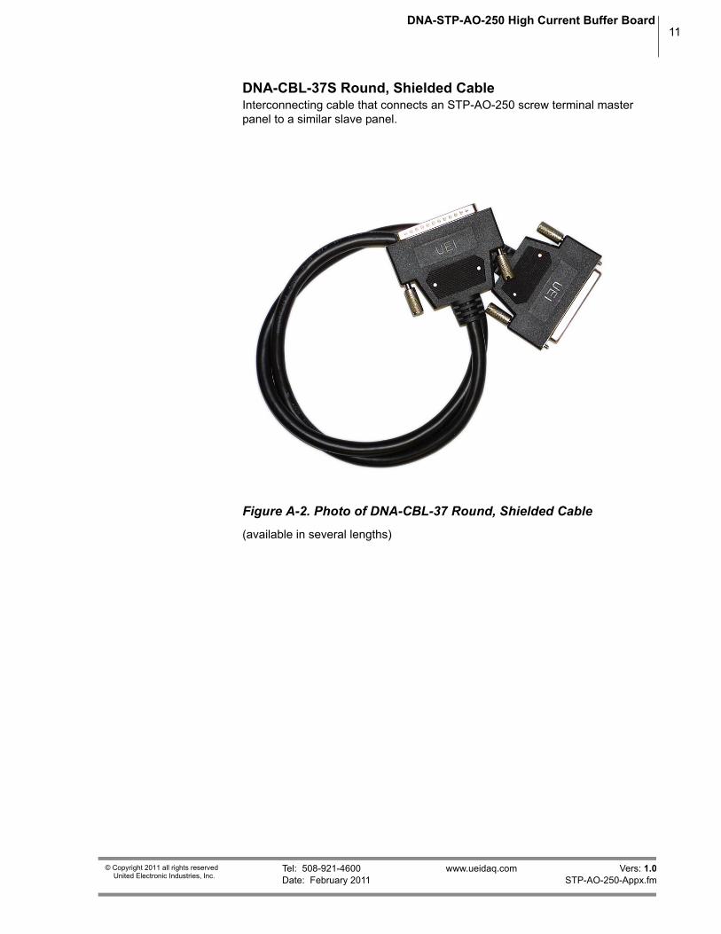
DNA-CBL-37S Round, Shielded CableInterconnecting cable that connects an STP-AO-250 screw terminal master panel to a similar slave panel.
Figure A-2. Photo of DNA-CBL-37 Round, Shielded Cable
(available in several lengths)
Tel: 508-921-4600 www.ueidaq.com Vers: 1.0Date: February 2011 STP-AO-250-Appx.fm
© Copyright 2011 all rights reservedUnited Electronic Industries, Inc.

16
Tel: 508-921-4600 www.ueidaq.com Vers: 1.0Date: February 2011 File: DNA-STP-AO-250-ManualIX.fm
© Copyright 2011 United Electronic Industries, Inc.
Index
AAccessories 10Accuracy Curves 3Architecture 9
CCable(s) 10Conventions 1
DDNA-STP-AO-250 Board 2
FFeatures 2
IInterconnection Diagram 4
OOrganization 1
PPhoto 2Pinout Diagrams 5
SSupport iiSupport email
[email protected] iiSupport FTP Site
ftp//ftp.ueidaq.com ii
Support Web Sitewww.ueidaq.com ii
TTechnical Specifications 5Tips 1
U
Use of Two STP-AO-250 Boards 4