
dlpa2000 Power Management And Led Driver Ic (rev. A) - … · d c b a 1 52 3 4 e f 6 g 7 h sw5 rlim...
58
DC Supplies BAT + – 1.1 V WVGA DDR DMD DLP2010 (WVGA DMD) Included in DLP® Chip Set 1.8 V 2.3 to 5.5 V Projector Module Electronics DLPA2000 PARKZ 1.1 V 1.8 V VCORE VIO Illumination Optics 3 BIAS, RST, OFS Thermistor Parallel I/F VCC_INTF EEPROM DLPC3430/ DLPC3435 VCC_FLSH SPI_1 I2C_1 1.8 V Other Supplies 1.1 V Reg Cal data (optional) FLASH, SDRAM Keypad Front-End Chip - OSD - AutoLock - Scaler -MicroController HDMI Receiver Triple ADC Charger DC_IN VDD On/Off HDMI VGA SD Card Reader, and so forth (optional) FLASH L1 Spare R/W GPIO TVP5151 Video Decoder BT.656 Keystone Sensor GPIO_8 (Normal Park) 1.8 V VSPI SPI_0 eDRAM L2 L3 GND CVBS RESETZ INTZ LED_SEL(2) CMP_PWM VLED WPC LABB 4 4 PROJ_ON PROJ_ON 1.8 V SYSPWR RED GREEN BLUE Sub-LVDS DATA CTRL I2C 28 HOST_IRQ Current Sense 18 CMP_OUT Product Folder Order Now Technical Documents Tools & Software Support & Community An IMPORTANT NOTICE at the end of this data sheet addresses availability, warranty, changes, use in safety-critical applications, intellectual property matters and other important disclaimers. PRODUCTION DATA. DLPA2000 DLPS043B – JUNE 2014 – REVISED FEBRUARY 2018 DLPA2000 Power Management and LED/Lamp Driver IC 1 1 Features 1• High Efficiency RGB LED/Lamp Driver with Buck- Boost DC-to-DC Converter, DMD Supplies, DPP Core Supply, 1.8-V Load Switch, and Measurement System in a Small Chip-Scale Package • Three Low-Impedance (30 mΩ Typical at 27°C) MOSFET Switches for Channel Selection • Independent, 10-Bit Current Control per Channel • 750-mA Max LED Current for DLPA2000 Embedded Applications • On-Chip Motor Driver • DMD Regulators – Requires Only a Single Inductor – VOFS: 10 V – VBIAS: 18 V – VRST: –14 V – Passive Discharge to GND When Disabled • DPP 1.1-V Core Supply – Synchronous Step-Down Converter with Integrated Switching FETs – Supports up to 600-mA Output Current • VLED Buck Boost Converter – Power Save Mode at Light Load Current • Low-Impedance Load Switch – V IN Range from 1.8 V to 3.6 V – Supports up to 200 mA of Current – Passive Discharge to GND When Disabled • DMD Reset Signal Generation and Power Supply Sequencing • 33-MHz Serial Peripheral Interface (SPI) • Multiplexer for Measuring Analog Signals – Battery Voltage – LED Voltage, LED Current – Light Sensor (for White Point Correction) – Internal Reference Voltage – External (Thermistor) Temperature Sensor • Monitoring and Protection Circuits – Hot Die Warning and Thermal – Low-Battery Warning – Programmable Battery Undervoltage Lockout (UVLO) – Load Switch UVLO – Overcurrent and Undervoltage Protection • DLPA2000 DSBGA Package – 56-Ball 0.4-mm Pitch – Die Size: 3.280 mm × 3.484 mm ± 0.03 mm 2 Applications DLP™ Display Projector DLP™ Mobile Sensing 3 Description The DLPA2000 is a dedicated PMIC/RGB LED/lamp driver for the DLP2010 and DLP2010NIR digital micromirror devices (DMD) when used with a DLPC3430, DLPC3435, or DLPC150 digital controller. For reliable operation of these chipsets, it is mandatory to use the DLPA2000. Device Information (1) PART NUMBER PACKAGE BODY SIZE (NOM) DLPA2000 DSBGA (56) 3.28 mm × 3.48 mm ± 0.03 mm (1) For all available packages, see the orderable addendum at the end of the data sheet. Figure 1. Simplified Schematic
Transcript of dlpa2000 Power Management And Led Driver Ic (rev. A) - … · d c b a 1 52 3 4 e f 6 g 7 h sw5 rlim...

DC Supplies
BAT+ ±
1.1 V
WVGADDR DMD
DLP2010(WVGADMD)
Included in DLP® Chip Set
1.8 V
2.3 to 5.5 V Projector Module Electronics
DLPA2000
PARKZ
1.1 V
1.8 V
VCORE
VIO
IlluminationOptics
3BIAS, RST, OFS
Thermistor
Parallel I/F
VCC_INTF
EEPROM
DLPC3430/DLPC3435
VCC_FLSH
SPI_1
I2C_1
1.8 VOtherSupplies
1.1 VReg
Cal data (optional)
FLASH, SDRAM
Keypad
Front-EndChip- OSD- AutoLock - Scaler-MicroController
HDMI Receiver
Triple ADC
ChargerDC_IN
VDD
On/Off
HDMI
VGA
SD Card Reader, and
so forth(optional)
FLASH
L1
Spare R/W GPIO
TVP5151 Video
Decoder
BT.656
KeystoneSensor
GPIO_8 (Normal Park)
1.8 V VSPI
SPI_0
eDRAM
L2
L3
GND
CVBS
RESETZINTZ
LED_SEL(2)
CMP_PWM
VLED
WPC
LABB
4
4
PROJ_ONPROJ_ON
1.8 V
SYSPWR
REDGREEN
BLUE
Sub-LVDS DATA
CTRL
I2C
28
HOST_IRQ
CurrentSense
18
CMP_OUT
Product
Folder
Order
Now
Technical
Documents
Tools &
Software
Support &Community
An IMPORTANT NOTICE at the end of this data sheet addresses availability, warranty, changes, use in safety-critical applications,intellectual property matters and other important disclaimers. PRODUCTION DATA.
DLPA2000DLPS043B –JUNE 2014–REVISED FEBRUARY 2018
DLPA2000 Power Management and LED/Lamp Driver IC
1
1 Features1• High Efficiency RGB LED/Lamp Driver with Buck-
Boost DC-to-DC Converter, DMD Supplies, DPPCore Supply, 1.8-V Load Switch, andMeasurement System in a Small Chip-ScalePackage
• Three Low-Impedance (30 mΩ Typical at 27°C)MOSFET Switches for Channel Selection
• Independent, 10-Bit Current Control per Channel• 750-mA Max LED Current for DLPA2000
Embedded Applications• On-Chip Motor Driver• DMD Regulators
– Requires Only a Single Inductor– VOFS: 10 V– VBIAS: 18 V– VRST: –14 V– Passive Discharge to GND When Disabled
• DPP 1.1-V Core Supply– Synchronous Step-Down Converter with
Integrated Switching FETs– Supports up to 600-mA Output Current
• VLED Buck Boost Converter– Power Save Mode at Light Load Current
• Low-Impedance Load Switch– VIN Range from 1.8 V to 3.6 V– Supports up to 200 mA of Current– Passive Discharge to GND When Disabled
• DMD Reset Signal Generation and Power SupplySequencing
• 33-MHz Serial Peripheral Interface (SPI)• Multiplexer for Measuring Analog Signals
– Battery Voltage– LED Voltage, LED Current– Light Sensor (for White Point Correction)– Internal Reference Voltage– External (Thermistor) Temperature Sensor
• Monitoring and Protection Circuits– Hot Die Warning and Thermal– Low-Battery Warning– Programmable Battery Undervoltage Lockout
(UVLO)– Load Switch UVLO– Overcurrent and Undervoltage Protection
• DLPA2000 DSBGA Package– 56-Ball 0.4-mm Pitch– Die Size: 3.280 mm × 3.484 mm ± 0.03 mm
2 ApplicationsDLP™ Display ProjectorDLP™ Mobile Sensing
3 DescriptionThe DLPA2000 is a dedicated PMIC/RGB LED/lampdriver for the DLP2010 and DLP2010NIR digitalmicromirror devices (DMD) when used with aDLPC3430, DLPC3435, or DLPC150 digitalcontroller. For reliable operation of these chipsets, itis mandatory to use the DLPA2000.
Device Information(1)
PART NUMBER PACKAGE BODY SIZE (NOM)
DLPA2000 DSBGA (56) 3.28 mm × 3.48 mm ± 0.03mm
(1) For all available packages, see the orderable addendum atthe end of the data sheet.
Figure 1. Simplified Schematic

2
DLPA2000DLPS043B –JUNE 2014–REVISED FEBRUARY 2018 www.ti.com
Product Folder Links: DLPA2000
Submit Documentation Feedback Copyright © 2014–2018, Texas Instruments Incorporated
Table of Contents1 Features .................................................................. 12 Applications ........................................................... 13 Description ............................................................. 14 Revision History..................................................... 25 Pin Configuration and Functions ......................... 36 Specifications......................................................... 5
6.1 Absolute Maximum Ratings ...................................... 56.2 Storage Conditions.................................................... 56.3 ESD Ratings.............................................................. 56.4 Recommended Operating Conditions....................... 56.5 Thermal Information .................................................. 66.6 Electrical Characteristics........................................... 66.7 Motor Driver Timing Requirements ......................... 116.8 Data Transmission Timing Requirements............... 126.9 Typical Characteristics ............................................ 13
7 Detailed Description ............................................ 147.1 Overview ................................................................. 147.2 Functional Block Diagram ....................................... 157.3 Feature Description................................................. 16
7.4 Device Functional Modes........................................ 277.5 Register Maps ......................................................... 29
8 Application and Implementation ........................ 418.1 Application Information............................................ 418.2 Typical Projector Application .................................. 418.3 Typical Mobile Sensing Application ....................... 43
9 Power Supply Recommendations ...................... 4610 Layout................................................................... 47
10.1 Layout Guidelines ................................................. 4710.2 Layout Example .................................................... 48
11 Device and Documentation Support ................. 4911.1 Device Support .................................................... 4911.2 Related Links ........................................................ 4911.3 Community Resources.......................................... 4911.4 Trademarks ........................................................... 4911.5 Electrostatic Discharge Caution............................ 5011.6 Glossary ................................................................ 50
12 Mechanical, Packaging, and OrderableInformation ........................................................... 51
4 Revision History
Changes from Revision A (August 2015) to Revision B Page
• Fixed body size dimension typo in Device Information, corrected 3.48 mm2 to 3.48 mm...................................................... 1• Added missing history tags to Revision A that were not listed............................................................................................... 1• Corrected package family to 'DSBGA' in Pin Functions Diagram, originally labeled as 'DSGBA' ......................................... 3• Added mechanical package designator YFF to Thermal Information .................................................................................... 6• Changed layout example to show correct image in Figure 46 ............................................................................................. 48
Changes from Original (June 2014) to Revision A Page
• Changed max current to 750 mA ........................................................................................................................................... 1• Added Mobile Sensing application ........................................................................................................................................ 1• Added typical Mobile sensing application ............................................................................................................................ 43• Updated the Power Supply Recommendations to remove information that did not apply to the DLPA2000 ..................... 46

D
C
B
A
4321 5
E
F
6
G
7
H
SW5 AOUT1RLIM
BOUT1
PGNDCM
VCORE
SW4LED_SEL1
RLIM_K
LS_INLS_OUT
VLED SENS1 SENS2VLEDPROJ_
ONDGND V2V5
L2 VSPICMP_OUT
L2PWM_
INAGND VINA
PGNDLSPI_CLK
SPI_CSZ
PGNDLSPI_DIN
SPI_DOUT
VOFS
L1RESET
ZINTZL1
CNTR_VRST
REF_VRST
VBIAS
VINL AGND1 VINRVINL SWN PGNDR SWP
SW6 V6V AOUT2RLIM
BOUT2
VINC SWC
LED_SEL0
VINM
RBOT_K
3
DLPA2000www.ti.com DLPS043B –JUNE 2014–REVISED FEBRUARY 2018
Product Folder Links: DLPA2000
Submit Documentation FeedbackCopyright © 2014–2018, Texas Instruments Incorporated
5 Pin Configuration and Functions
YFF PACKAGE56-PIN DSBGABOTTOM VIEW
Pin FunctionsPIN
I/O DESCRIPTIONNAME NUMBER
VINLA1
I Power supply input for VLED BUCK-BOOST power stage. Connect to system power.A2
AGND1 A3 GND Analog ground. Connect to ground plane.VINR A4 I Power supply input for DMD switch mode power supply (SMPS). Connect to system power.SWN A5 I Connection for the DMD SMPS-inductor (high-side switch).PGNDR A6 GND Power ground for DMD SMPS. Connect to ground plane.SWP A7 O Connection for the DMD SMPS-inductor (low-side switch).
L1B1
O Connection for VLED BUCK-BOOST inductor.B2
RESETZ B3 O Reset output to the DLP system (active low). Pin is held low to reset DLP system.INTZ B4 O Interrupt output signal (open drain). Connect to pull-up resistor or short to ground.CNTR_VRST B5 O Connection to VRST for fast discharge function.REF_VRST B6 I Reference pin for the VRST regulator. Connect to VRST rail through 100-kΩ resistor.VBIAS B7 O VBIAS output rail. Connect to ceramic capacitor.
PGNDLC1
GND Power ground for VLED BUCK-BOOST. Connect to ground plane.C2
SPI_CLK C3 I Clock input for SPI interface.SPI_CSZ C4 I SPI chip select (active low).SPI_DIN C5 I SPI data input.

4
DLPA2000DLPS043B –JUNE 2014–REVISED FEBRUARY 2018 www.ti.com
Product Folder Links: DLPA2000
Submit Documentation Feedback Copyright © 2014–2018, Texas Instruments Incorporated
Pin Functions (continued)PIN
I/O DESCRIPTIONNAME NUMBER
SPI_DOUT C6 O SPI data output.VOFS C7 O VOFS output rail. Connect to ceramic capacitor.
L2D1
I Connection for VLED BUCK-BOOST inductor.D2
VSPI D3 I Power supply input for SPI interface. Connect to system I/O voltage.CMP_OUT D4 O Analog-comparator output.PWM_IN D5 I Reference voltage input for analog comparator.AGND D6 GND Analog ground. Connect to ground plane.VINA D7 POWER Power supply input for sensitive analog circuitry.
VLEDE1
O VLED BUCK-BOOST converter output pin.E2
SENS1 E3 I Input signal from light sensor.SENS2 E4 I Input signal from temperature sensor.PROJ_ON E5 I Input signal to enable or disable the IC and DLP projector.DGND E6 GND Digital ground. Connect to ground plane.V2V5 E7 O Internal supply filter pin for digital logic; typical 2.5 V.SW4 F1 O Low-side MOSFET switch for LED cathode. Connect to RGB LED assembly.
RLIM_K F2 IKelvin sense connection to top side of LED current sense resistor.For best accuracy, route this trace directly to the top of the current sense resistor andseparate it from the normal trace from the current sense resistor to the RLIM pins.
LED_SEL1 F3 I Digital input to the RGB STROBE DECODER.LED_SEL0 F4 I Digital input to the RGB STROBE DECODER.BOUT1 F5 O Motor driver B phase output1.LS_IN F6 I Load switch.LS_OUT F7 O Load switch.SW5 G1 O Low-side MOSFET switch for LED cathode. Connect to RGB LED assembly.
RLIM G2 O Connection to LED ‘current sense’ resistor.Bottom side of sense resistor is connected to GND.
RBOT_K G3 I Kelvin sense connection to ground side of LED current sense resistor.AOUT1 G4 O Motor driver A phase output1.BOUT2 G5 O Motor driver B phase output2.VCORE G6 I VCORE BUCK converter feedback pin.PGNDCM G7 GND Power ground for VCORE BUCK and motor driver.SW6 H1 O Low-side MOSFET switch for LED cathode. Connect to RGB LED assembly.
RLIM H2 O Connection to LED current sense resistor.Bottom side of sense resistor is connected to GND.
V6V H3 O Internal supply filter pin for gate driver circuitry. Typical 6.25 V.AOUT2 H4 O Motor driver A phase output2.VINM H5 I Power supply input for motor driver power stage. Connect to system power.VINC H6 I Power supply input for VCORE BUCK power stage. Connect to system power.SWC H7 I/O Connection for 1.1-V BUCK inductor.
5
DLPA2000www.ti.com DLPS043B –JUNE 2014–REVISED FEBRUARY 2018
Product Folder Links: DLPA2000
Submit Documentation FeedbackCopyright © 2014–2018, Texas Instruments Incorporated
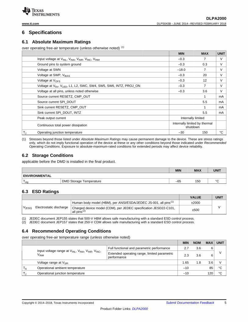
(1) Stresses beyond those listed under Absolute Maximum Ratings may cause permanent damage to the device. These are stress ratingsonly, which do not imply functional operation of the device at these or any other conditions beyond those indicated under RecommendedOperating Conditions. Exposure to absolute-maximum-rated conditions for extended periods may affect device reliability.
6 Specifications
6.1 Absolute Maximum Ratingsover operating free-air temperature (unless otherwise noted) (1)
MIN MAX UNITInput voltage at VINL, VINA, VINR, VINC, VINM –0.3 7 VGround pins to system ground –0.3 0.3 VVoltage at SWN –18.0 7 VVoltage at SWP, VBIAS –0.3 20 VVoltage at VOFS –0.3 12 VVoltage at V6V, VLED, L1, L2, SWC, SW4, SW5, SW6, INTZ, PROJ_ON –0.3 7 VVoltage at all pins, unless noted otherwise –0.3 3.6 VSource current RESETZ, CMP_OUT 1 mASource current SPI_DOUT 5.5 mASink current RESETZ, CMP_OUT 1 mASink current SPI_DOUT, INTZ 5.5 mAPeak output current Internally limited
Continuous total power dissipation Internally limited by thermalshutdown
TJ Operating junction temperature –30 150 °C
6.2 Storage Conditionsapplicable before the DMD is installed in the final product.
MIN MAX UNITENVIRONMENTALTstg DMD Storage Temperature –65 150 °C
(1) JEDEC document JEP155 states that 500-V HBM allows safe manufacturing with a standard ESD control process.(2) JEDEC document JEP157 states that 250-V CDM allows safe manufacturing with a standard ESD control process.
6.3 ESD RatingsVALUE UNIT
V(ESD) Electrostatic dischargeHuman body model (HBM), per ANSI/ESDA/JEDEC JS-001, all pins (1) ±2000
VCharged device model (CDM), per JEDEC specification JESD22-C101,all pins (2) ±500
6.4 Recommended Operating Conditionsover operating free-air temperature range (unless otherwise noted)
MIN NOM MAX UNIT
Input voltage range at VINL, VINA, VINR, VINC,VINM
Full functional and parametric performance 2.7 3.6 6VExtended operating range, limited parametric
performance 2.3 3.6 6
Voltage range at VSPI 1.65 1.8 3.6 VTA Operational ambient temperature –10 85 °CTJ Operational junction temperature –10 120 °C

6
DLPA2000DLPS043B –JUNE 2014–REVISED FEBRUARY 2018 www.ti.com
Product Folder Links: DLPA2000
Submit Documentation Feedback Copyright © 2014–2018, Texas Instruments Incorporated
(1) For more information about traditional and new thermal metrics, see the IC Package Thermal Metrics application report, SPRA953.(2) Estimated when mounted on high K JEDEC board per JESD 51-7 with thickness of 1.6 mm, 4 layers, size of 76.2 mm × 114.3 mm, and
2-oz. copper for top and bottom plane. Actual thermal impedance will depend on PCB used in the application.
6.5 Thermal Information
THERMAL METRIC (1) DLPA2000UNIT
YFF (DSBGA)56 PINS
RθJA Junction-to-ambient thermal resistance (2) 45 °C/W
(1) Fully functional but limited parametric performance(2) Including rectifying diode(3) To reduce ripple the COUT can be increased. VRIPPLE is inversely proportional to COUT.
6.6 Electrical Characteristicsover operating free-air temperature range (unless otherwise noted) (see (1) (2))
PARAMETER TEST CONDITIONS MIN TYP MAX UNITSUPPLIESINPUT VOLTAGE
VIInput voltage range
VINA, VINR, VINL, VINC2.7 3.6 6
VExtended input voltage range (1) 2.3 3.6 6
VLOW_BATLow-battery warning threshold VINA falling 3 VHysteresis VINA rising 100 mV
Vhys(UVLO)Undervoltage lockout threshold VINA falling (through 5-bit trim function) 2.3 4.5 VHysteresis VINA rising 100 mV
VSTARTUP Startup voltage VBIAS, VOFS, VRST; loaded with 2 mA 2.5 VINPUT CURRENTIQ ACTIVE mode Motor current excluded 15 mAISTD STANDBY mode 900 µAIIDLE IDLE mode 10 µAINTERNAL SUPPLIESVV6V Internal supply, analog 6.25 VCLDO_V6V Filter capacitor for V6V LDO 100 nFVV2V5 Internal supply, logic 2.5 VCLDO_V2V5 Filter capacitor for V2V5 LDO 2.2 µFDMD REGULATOR
RDS(ON) MOSFET ON-resistanceSwitch E (from VINR to SWN) 1000
mΩSwitch F (from SWP to PGNDR) 320
VFW Forward voltage drop
Switch G (2) (from SWP to VBIAS)VINR = 5 V, VSWP = 2 V, IF = 100 mA 1.3
VSwitch H (from SWP to VOFS)VINR = 5 V, VSWP = 2 V, IF = 100 mA 1.3
tDIS Rail discharge time VIN = 2.9 V; COUT = 110 nF 40 µstPG Power-good timeout Not tested in production 6 msILIMIT Switch current limit 312 mAL Inductor value 10 µHVOFS REGULATOR
VOFS
Output voltage 10 VDC output voltage accuracy IOUT = 2 mA –2% 2%DC load regulation VIN = 3.6 V, IOUT = 0 to 2 mA –19 V/A
DC line regulation VINA, VINL, VINR, VINC 2.7 to 6.0 V, IOUT =2 mA 35 mV/V
VRIPPLE Output ripple VIN = 3.6 V, IOUT = 2 mA, COUT = 440 nF (3) 375 mVppIOUT Output current 0 3 mA
7
DLPA2000www.ti.com DLPS043B –JUNE 2014–REVISED FEBRUARY 2018
Product Folder Links: DLPA2000
Submit Documentation FeedbackCopyright © 2014–2018, Texas Instruments Incorporated
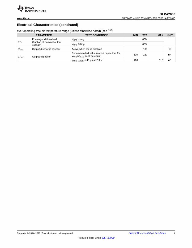
Electrical Characteristics (continued)over operating free-air temperature range (unless otherwise noted) (see (1)(2))
PARAMETER TEST CONDITIONS MIN TYP MAX UNIT
PGPower-good threshold(fraction of nominal outputvoltage)
VOFS rising 86%
VOFS falling 66%
RDIS Output discharge resistor Active when rail is disabled 100 Ω
COUT Output capacitorRecommended value (output capacitors forVOFS/VBIAS must be equal) 110 220 nF
tDISCHARGE < 40 µs at 2.9 V 100 110 nF
8
DLPA2000DLPS043B –JUNE 2014–REVISED FEBRUARY 2018 www.ti.com
Product Folder Links: DLPA2000
Submit Documentation Feedback Copyright © 2014–2018, Texas Instruments Incorporated
Electrical Characteristics (continued)over operating free-air temperature range (unless otherwise noted) (see (1)(2))
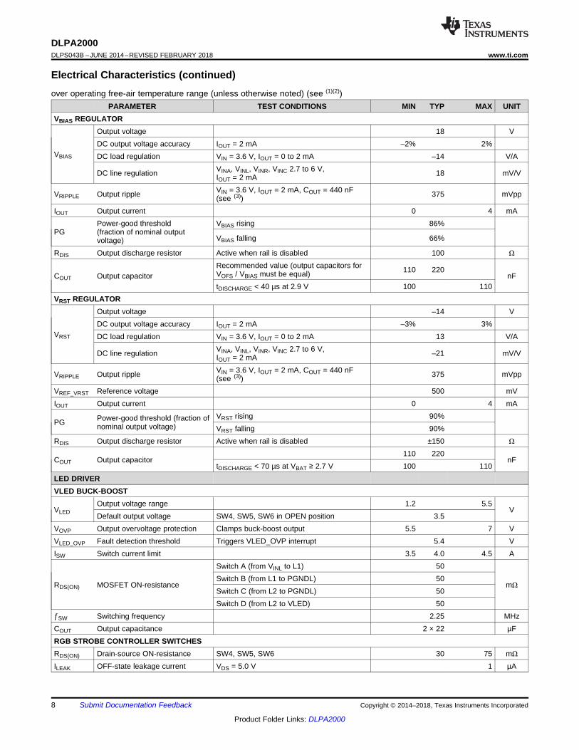
PARAMETER TEST CONDITIONS MIN TYP MAX UNITVBIAS REGULATOR
VBIAS
Output voltage 18 VDC output voltage accuracy IOUT = 2 mA –2% 2%DC load regulation VIN = 3.6 V, IOUT = 0 to 2 mA –14 V/A
DC line regulation VINA, VINL, VINR, VINC 2.7 to 6 V,IOUT = 2 mA 18 mV/V
VRIPPLE Output ripple VIN = 3.6 V, IOUT = 2 mA, COUT = 440 nF(see (3)) 375 mVpp
IOUT Output current 0 4 mA
PGPower-good threshold(fraction of nominal outputvoltage)
VBIAS rising 86%
VBIAS falling 66%
RDIS Output discharge resistor Active when rail is disabled 100 Ω
COUT Output capacitorRecommended value (output capacitors forVOFS / VBIAS must be equal) 110 220
nFtDISCHARGE < 40 µs at 2.9 V 100 110
VRST REGULATOR
VRST
Output voltage –14 VDC output voltage accuracy IOUT = 2 mA –3% 3%DC load regulation VIN = 3.6 V, IOUT = 0 to 2 mA 13 V/A
DC line regulation VINA, VINL, VINR, VINC 2.7 to 6 V,IOUT = 2 mA –21 mV/V
VRIPPLE Output ripple VIN = 3.6 V, IOUT = 2 mA, COUT = 440 nF(see (3)) 375 mVpp
VREF_VRST Reference voltage 500 mVIOUT Output current 0 4 mA
PG Power-good threshold (fraction ofnominal output voltage)
VRST rising 90%VRST falling 90%
RDIS Output discharge resistor Active when rail is disabled ±150 Ω
COUT Output capacitor110 220
nFtDISCHARGE < 70 µs at VBAT ≥ 2.7 V 100 110
LED DRIVERVLED BUCK-BOOST
VLEDOutput voltage range 1.2 5.5
VDefault output voltage SW4, SW5, SW6 in OPEN position 3.5
VOVP Output overvoltage protection Clamps buck-boost output 5.5 7 VVLED_OVP Fault detection threshold Triggers VLED_OVP interrupt 5.4 VISW Switch current limit 3.5 4.0 4.5 A
RDS(ON) MOSFET ON-resistance
Switch A (from VINL to L1) 50
mΩSwitch B (from L1 to PGNDL) 50Switch C (from L2 to PGNDL) 50Switch D (from L2 to VLED) 50
ƒSW Switching frequency 2.25 MHzCOUT Output capacitance 2 × 22 µFRGB STROBE CONTROLLER SWITCHESRDS(ON) Drain-source ON-resistance SW4, SW5, SW6 30 75 mΩ
ILEAK OFF-state leakage current VDS = 5.0 V 1 µA
9
DLPA2000www.ti.com DLPS043B –JUNE 2014–REVISED FEBRUARY 2018
Product Folder Links: DLPA2000
Submit Documentation FeedbackCopyright © 2014–2018, Texas Instruments Incorporated
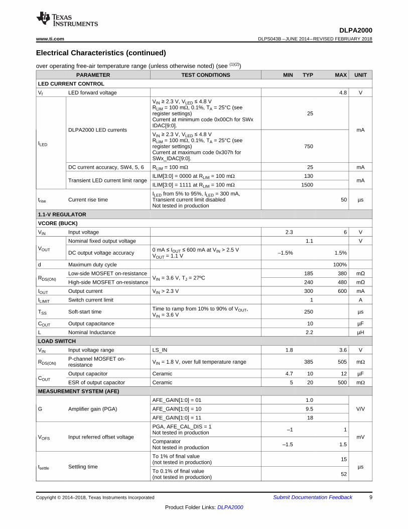
Electrical Characteristics (continued)over operating free-air temperature range (unless otherwise noted) (see (1)(2))
PARAMETER TEST CONDITIONS MIN TYP MAX UNITLED CURRENT CONTROLVf LED forward voltage 4.8 V
ILED
DLPA2000 LED currents
VIN ≥ 2.3 V, VLED ≤ 4.8 VRLIM = 100 mΩ, 0.1%, TA = 25°C (seeregister settings)Current at minimum code 0x00Ch for SWxIDAC[9:0].
25
mAVIN ≥ 2.3 V, VLED ≤ 4.8 VRLIM = 100 mΩ, 0.1%, TA = 25°C (seeregister settings)Current at maximum code 0x307h forSWx_IDAC[9:0].
750
DC current accuracy, SW4, 5, 6 RLIM = 100 mΩ 25 mA
Transient LED current limit rangeILIM[3:0] = 0000 at RLIM = 100 mΩ 130
mAILIM[3:0] = 1111 at RLIM = 100 mΩ 1500
trise Current rise timeILED from 5% to 95%, ILED = 300 mA,Transient current limit disabledNot tested in production
50 µs
1.1-V REGULATORVCORE (BUCK)VIN Input voltage 2.3 6 V
VOUT
Nominal fixed output voltage 1.1 V
DC output voltage accuracy 0 mA ≤ IOUT ≤ 600 mA at VIN > 2.5 VVOUT = 1.1 V –1.5% 1.5%
d Maximum duty cycle 100%
RDS(ON)Low-side MOSFET on-resistance
VIN = 3.6 V, TJ = 27ºC185 380 mΩ
High-side MOSFET on-resistance 240 480 mΩIOUT Output current VIN > 2.3 V 300 600 mAILIMIT Switch current limit 1 A
TSS Soft-start time Time to ramp from 10% to 90% of VOUT,VIN = 3.6 V 250 µs
COUT Output capacitance 10 µFL Nominal Inductance 2.2 µHLOAD SWITCHVIN Input voltage range LS_IN 1.8 3.6 V
RDS(ON)P-channel MOSFET on-resistance VIN = 1.8 V, over full temperature range 385 505 mΩ
COUTOutput capacitor Ceramic 4.7 10 12 µFESR of output capacitor Ceramic 5 20 500 mΩ
MEASUREMENT SYSTEM (AFE)
G Amplifier gain (PGA)AFE_GAIN[1:0] = 01 1.0
V/VAFE_GAIN[1:0] = 10 9.5AFE_GAIN[1:0] = 11 18
VOFS Input referred offset voltage
PGA, AFE_CAL_DIS = 1Not tested in production –1 1
mVComparatorNot tested in production –1.5 1.5
tsettle Settling time
To 1% of final value(not tested in production) 15
µsTo 0.1% of final value(not tested in production) 52
10
DLPA2000DLPS043B –JUNE 2014–REVISED FEBRUARY 2018 www.ti.com
Product Folder Links: DLPA2000
Submit Documentation Feedback Copyright © 2014–2018, Texas Instruments Incorporated
Electrical Characteristics (continued)over operating free-air temperature range (unless otherwise noted) (see (1)(2))
PARAMETER TEST CONDITIONS MIN TYP MAX UNIT
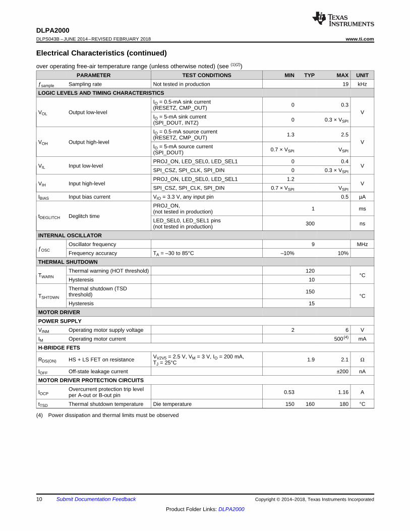
(4) Power dissipation and thermal limits must be observed
ƒsample Sampling rate Not tested in production 19 kHzLOGIC LEVELS AND TIMING CHARACTERISTICS
VOL Output low-level
IO = 0.5-mA sink current(RESETZ, CMP_OUT) 0 0.3
VIO = 5-mA sink current(SPI_DOUT, INTZ) 0 0.3 × VSPI
VOH Output high-level
IO = 0.5-mA source current(RESETZ, CMP_OUT) 1.3 2.5
VIO = 5-mA source current(SPI_DOUT) 0.7 × VSPI VSPI
VIL Input low-levelPROJ_ON, LED_SEL0, LED_SEL1 0 0.4
VSPI_CSZ, SPI_CLK, SPI_DIN 0 0.3 × VSPI
VIH Input high-levelPROJ_ON, LED_SEL0, LED_SEL1 1.2
VSPI_CSZ, SPI_CLK, SPI_DIN 0.7 × VSPI VSPI
IBIAS Input bias current VIO = 3.3 V, any input pin 0.5 µA
tDEGLITCH Deglitch time
PROJ_ON,(not tested in production) 1 ms
LED_SEL0, LED_SEL1 pins(not tested in production) 300 ns
INTERNAL OSCILLATOR
ƒOSCOscillator frequency 9 MHzFrequency accuracy TA = –30 to 85°C –10% 10%
THERMAL SHUTDOWN
TWARNThermal warning (HOT threshold) 120
°CHysteresis 10
TSHTDWN
Thermal shutdown (TSDthreshold) 150
°CHysteresis 15
MOTOR DRIVERPOWER SUPPLYVINM Operating motor supply voltage 2 6 VIM Operating motor current 500 (4) mAH-BRIDGE FETS
RDS(ON) HS + LS FET on resistance VV2V5 = 2.5 V, VM = 3 V, IO = 200 mA,TJ = 25°C 1.9 2.1 Ω
IOFF Off-state leakage current ±200 nAMOTOR DRIVER PROTECTION CIRCUITS
IOCPOvercurrent protection trip levelper A-out or B-out pin 0.53 1.16 A
tTSD Thermal shutdown temperature Die temperature 150 160 180 °C

x
x
x
x
11
DLPA2000www.ti.com DLPS043B –JUNE 2014–REVISED FEBRUARY 2018
Product Folder Links: DLPA2000
Submit Documentation FeedbackCopyright © 2014–2018, Texas Instruments Incorporated
6.7 Motor Driver Timing RequirementsThe table lists the timing numbers to drive the motor voltages correctly, while Figure 2 shows the timing sequences.
NUMBER MIN MAX UNIT1 t1 Delay time, xPHASE high to xOUT1 low 300 ns2 t2 Delay time, xPHASE high to xOUT2 high 200 ns3 t3 Delay time, xPHASE low to xOUT1 high 200 ns4 t4 Delay time, xPHASE low to xOUT1 low 300 ns5 t5 Delay time, xENBL high to xOUTx high 200 ns6 t6 Delay time, xENBL high to xOUTx low 300 ns7 t7 Output enable time 300 ns8 t8 Output disable time 300 ns9 t9 Delay time, xINx high to xOUTx high 160 ns
10 t10 Delay time, xINx low to xOUTx low 160 ns11 tR Output rise time 30 188 ns12 tF Output fall time 30 188 ns
Figure 2. Bridge Control

tCSCR
tCDS tCDH
tCFDO
tCFCS
tCSZ
HiZ HiZ
SPI_CSZ
(SS)
SPI_CLK
(SCLK)
SPI_DIN
(MOSI)
SPI_DOUT
(MISO)
tiStiH
tCLKL tCLKH
12
DLPA2000DLPS043B –JUNE 2014–REVISED FEBRUARY 2018 www.ti.com
Product Folder Links: DLPA2000
Submit Documentation Feedback Copyright © 2014–2018, Texas Instruments Incorporated
(1) The DPPxxxx processors send and receive data on the falling edge of the clock.
6.8 Data Transmission Timing RequirementsVBAT = 3.6 ± 5%, TA = 25 ºC, CL = 10 pF (unless otherwise noted)
MIN NOM MAX UNITƒCLK Serial clock frequency 0 36 MHztCLKL Pulse width low, SPI_CLK, 50% level 10 nstCLKH Pulse width high, SPI_CLK, 50% level 10 nstt Transition time, 20% to 80% level, all signals 0.2 4 nstCSCR SPI_CSZ falling to SPI_CLK rising, 50% level 8 nstCFCS SPI_CLK falling to SPI_CSZ rising, 50% level 1 nstCDS SPI_DIN data setup time, 50% level 7 nstCDH SPI_DIN data hold time, 50% level 6 nstiS SPI_DOUT data setup time (1), 50% level 10 nstiH SPI_DOUT data hold time (1), 50% level 0 nstCFDO SPI_CLK falling to SPI_DOUT data valid, 50% level 13 nstCSZ SPI_CSZ rising to SPI_DOUT HiZ 6 ns
Figure 3. SPI Timing Diagram

VIN(V)
Max
LE
D C
urre
nt(A
)
Gamma Curves
2 3 4 5 60
0.2
0.4
0.6
0.8
D001
13
DLPA2000www.ti.com DLPS043B –JUNE 2014–REVISED FEBRUARY 2018
Product Folder Links: DLPA2000
Submit Documentation FeedbackCopyright © 2014–2018, Texas Instruments Incorporated
6.9 Typical CharacteristicsThe maximum output current of the buck-boost is a function of input voltage (VIN) and output voltage (VLED). The relationshipbetween VIN, VLED, and MAX ILED is shown in Figure 4. Note that VLED is the output of the buck-boost regulator, which includesthe voltage drop across the sense resistor RLIM (100 mΩ typical), internal strobe control switch(75 mΩ max), and the forward voltage of the LED.
2.3 V < VLED < 4.8 V
Figure 4. Maximum LED Output Current as a Function ofInput Voltage (VIN) and Buck-Boost Output Voltage (VLED)

14
DLPA2000DLPS043B –JUNE 2014–REVISED FEBRUARY 2018 www.ti.com
Product Folder Links: DLPA2000
Submit Documentation Feedback Copyright © 2014–2018, Texas Instruments Incorporated
7 Detailed Description
7.1 OverviewThe DLPA2000 is a power management and LED driver IC optimized for DLP video and data display systemsand meant for use in either embedded or accessory projector applications. DLPA2000 is part of the chipsetcomprising of either DLP2010 (0.2 WVGA) DMD and DLPC3430/DLPC3435 controller or the DLP2010NIR (0.2WVGA NIR) DMD and DLPC150 controller. The DLPA2000 contains a complete LED driver including highefficiency power convertors. The DLPA2000 can supply up to 750 mA per LED. Integrated high-current switchesare included for sequentially selecting R, G, and B LEDs. The DLPA2000 also contains three regulated DCsupplies for the DMD reset circuitry: VBIAS, VRST and VOFS, as well as a regulated DC supply of 1.1 V and a loadswitch for the 1.8 V to support the DLPC3430 or DLPC3435 controller. The DLPA2000 also contains a motordriver which can be used to drive the focus lens motor. The DLPA2000 has a SPI used for setting theconfiguration. Using SPI, currents can be set independently for each LED with 10-bit resolution. Other featuresincluded are the generation of the system reset, power sequencing, input signals for sequentially selecting theactive LED, IC self-protections, and an analog MUX for routing analog information to an external ADC.
From host
To host
From light sensor
From host
From temperature sensor
VIO (depends on DPP requirements) SPI_CSZ
SPI_CLK
SPI_DIN
SPI_DOUT
VSPI
LED_SEL0
LED_SEL1
DIGITALCORE
RESETZPROJ_ON
INTZ
DGND
SPI
0.1u
To DPP (optional)
To system
V2V5
VREF
LOW_BAT
UVLO
VINA REFERENCESYSTEM
AGND1
AGND
LDO_V6V
LDO_V2V5
V6V
V2V5
1µ
From system power
100n
2.2µ
VLED_OVPVREF
VLED
VREF
SWCVCOREBUCK
VCORE
2.2uHVout DCDC1 (0.9-1.2V @ 450mA)
PGNDC/PGNDM
From system powerVINC
10µF
F
G
H
ESWN
SWP
VBIAS
VOFS
PGNDR
VINR
REF_VRST
10µ
From system power
220n
VRST
100k
220n
220n
VBIAS
VOFS
10µ
DMDRESET
REGULATORS
2.2µ
L1
VLED BUCK-BOOST
B
C
DVLED
A
L2
PGNDL
VINL
22µ
22µ
1µ
From system power
RLIM
SW5
SW6
RLIM
SW4
RGBSTROBE
DECODER
RLIM_K
from any 1.8V-3.3V supply
to system load
LS_IN
LS_OUT
10PF
Load Switch
Full H-Bridge
Aout1
Aout2
Bout1
Bout2Full H-Bridge
MOTOR DRIVER
RBOT_K
SW6RLIM_KVREF
To host
SW4SW5
SENS1
VINA/3VLED/3
SENS2
CMP_OUT
PWM_IN
AFE_SEL[3:0]AFE_GAIN [1:0]
AFE
MUX
CNTR_VRST
SET_LOW_BAT_USB
VINMFrom system power
From host
From host
From host
From host
From host
From host
5k
15
DLPA2000www.ti.com DLPS043B –JUNE 2014–REVISED FEBRUARY 2018
Product Folder Links: DLPA2000
Submit Documentation FeedbackCopyright © 2014–2018, Texas Instruments Incorporated
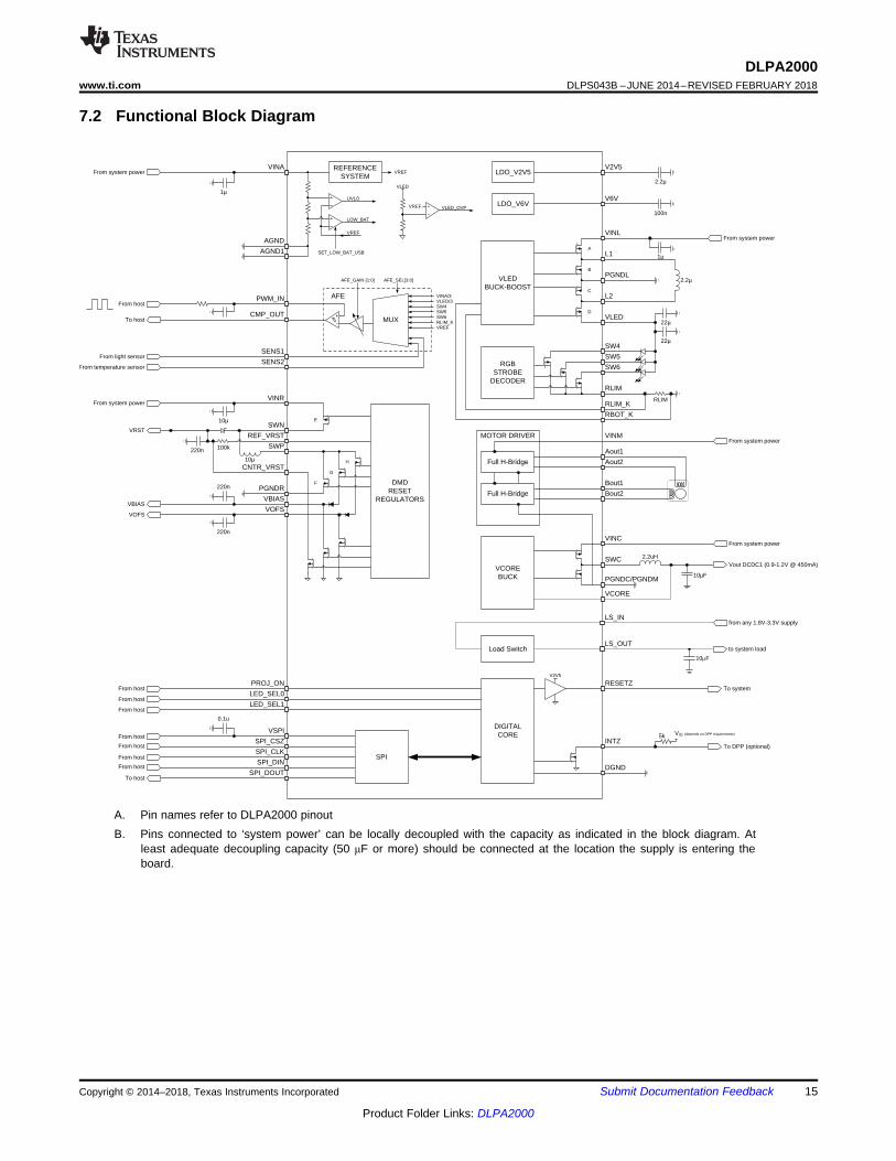
7.2 Functional Block Diagram
A. Pin names refer to DLPA2000 pinoutB. Pins connected to ‘system power’ can be locally decoupled with the capacity as indicated in the block diagram. At
least adequate decoupling capacity (50 μF or more) should be connected at the location the supply is entering theboard.

PROJ_ON
VBIAS
VOFS
VRST
VCORE
VLED
STATE STANDBY ACTIVE2
V2V5
LS_OUT (1.8 V)
INTZ
RESETZ
OFF OFF
10 ms25 ms
ACTIVE1
5 ms (min)
DMD_ENin register 0x01h
10 ms
Startup DPP
System Power (VINx)
10 ms DMD initialization
by DPP10 ms
Pad DMD_EN by DPP through
SPI write
Stop Regulating VBIAS
Stop Regulating VRST
145 ms
16
DLPA2000DLPS043B –JUNE 2014–REVISED FEBRUARY 2018 www.ti.com
Product Folder Links: DLPA2000
Submit Documentation Feedback Copyright © 2014–2018, Texas Instruments Incorporated
7.3 Feature Description
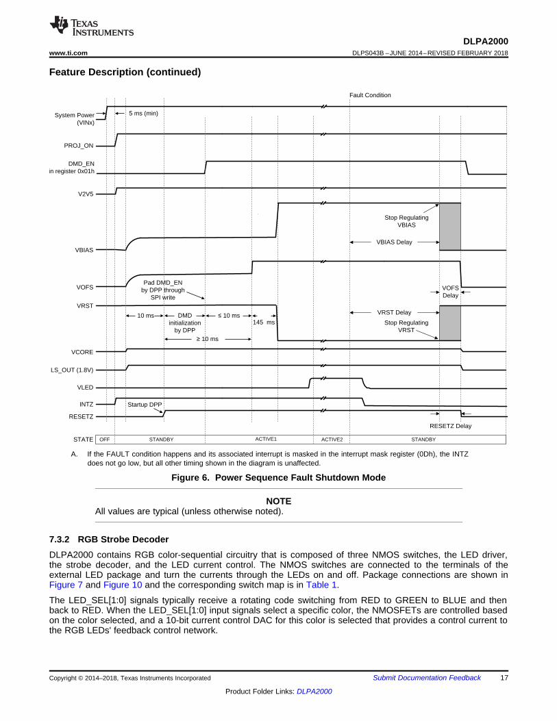
7.3.1 DMD RegulatorsDLPA2000 contains three switch-mode power supplies that power the DMD. These rails are VOFS, VBIAS, andVRST. After pulling the PROJ_ON pin high, the DMD is first initialized followed by a power-up of the VOFS lineafter a small delay of less than 10 ms followed by VBIAS and VRST with an additional delay of 145 ms. The LEDdriver and STROBE DECODER circuit can only be enabled after all three rails are enabled. There are twopower-down sequences, the normal power-down timing initiated after pulling the PROJ_ON pin low, and a fastpower-down mode where if any one of the rails encounters a fault such as an output short, all three rails aredischarged simultaneously. The detailed power-up and power-down diagrams are shown in Figure 5 andFigure 6.
Figure 5. Power Sequence Normal Shutdown Mode
NOTEAll values are typical (unless otherwise noted).
PROJ_ON
VBIAS
VOFS
VRST
VCORE
VLED
STATE STANDBY ACTIVE2
V2V5
LS_OUT (1.8V)
INTZ
RESETZ
OFF STANDBYACTIVE1
5 ms (min)
DMD_ENin register 0x01h
10 ms
Startup DPP
System Power (VINx)
10 ms DMD initialization
by DPP10 ms
Pad DMD_EN by DPP through
SPI write
Stop Regulating VBIAS
Stop Regulating VRST
Fault Condition
VBIAS Delay
VRST Delay
VOFS Delay
RESETZ Delay
145 ms
17
DLPA2000www.ti.com DLPS043B –JUNE 2014–REVISED FEBRUARY 2018
Product Folder Links: DLPA2000
Submit Documentation FeedbackCopyright © 2014–2018, Texas Instruments Incorporated
Feature Description (continued)
A. If the FAULT condition happens and its associated interrupt is masked in the interrupt mask register (0Dh), the INTZdoes not go low, but all other timing shown in the diagram is unaffected.
Figure 6. Power Sequence Fault Shutdown Mode
NOTEAll values are typical (unless otherwise noted).
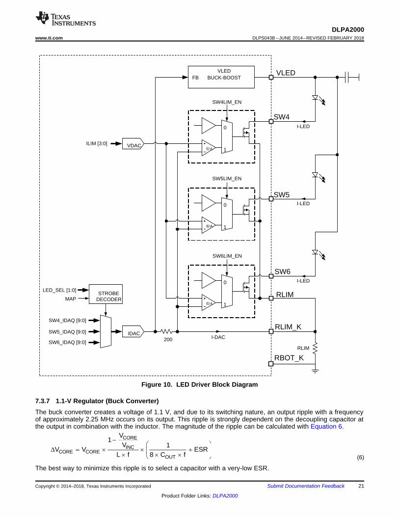
7.3.2 RGB Strobe DecoderDLPA2000 contains RGB color-sequential circuitry that is composed of three NMOS switches, the LED driver,the strobe decoder, and the LED current control. The NMOS switches are connected to the terminals of theexternal LED package and turn the currents through the LEDs on and off. Package connections are shown inFigure 7 and Figure 10 and the corresponding switch map is in Table 1.
The LED_SEL[1:0] signals typically receive a rotating code switching from RED to GREEN to BLUE and thenback to RED. When the LED_SEL[1:0] input signals select a specific color, the NMOSFETs are controlled basedon the color selected, and a 10-bit current control DAC for this color is selected that provides a control current tothe RGB LEDs' feedback control network.

I-LE
D
TIME
SW4 SW5 SW6
BBM dead time
SW4SW6
SW5 SW6SW4
VLED
SW4
SW5
SW6
R G B
RLIM
RLIMRLIM_K
RBOT_K
18
DLPA2000DLPS043B –JUNE 2014–REVISED FEBRUARY 2018 www.ti.com
Product Folder Links: DLPA2000
Submit Documentation Feedback Copyright © 2014–2018, Texas Instruments Incorporated
Feature Description (continued)
Figure 7. Switch Connection for a Common-Anode LED Assembly
Table 1. Switch Positions for Common Anode RGB LEDs (MAP = 0)Common Anode
LED_SEL[1:0] SW6 SW5 SW4 IDAC INPUT0x00h Open Open Open N/A0x01h Open Open Closed SW4_IDAC[9:0]0x02h Open Closed Open SW5_IDAC[9:0]0x03h Closed Open Open SW6_IDAC[9:0]
The switching of the three NMOS switches is controlled such that switches are returned to the open position firstbefore the closed connections are made (break before make). The dead time between opening and closingswitches is controlled through the BBM register. Switches that already are in the closed position (and are toremain in the closed state according to the SWCNTRL register) are not opened during the BBM delay time.
Figure 8. BBM Timing (See Register 0Bh in Figure 27)
7.3.3 LED Current ControlDLPA2000 provides time-sequential circuitry to drive three LEDs with independent current control. A systembased on a common anode LED configuration is shown in Figure 10 and consists of a buck-boost converter,which provides the voltage to drive the LEDs, three switches connected to the cathodes of the LEDs, an RLIMresistor used to sense the LED current, and a current DAC to control the LED current. The voltage measured atthe pin V(RLIM_K) is used by the regulator loop.
The STROBE DECODER controls the switch positions as described in the previous section (RGB StrobeDecoder). With all switches in the open position, the buck-boost output assumes an output voltage of 3.5 V.

IN2 OUT IN2OUT OUT2
IN2 OUT
V V VV II
0.8 V 2 V f L
u
u u u u
OUT IN1 OUTOUT1
IN1
V V VII
0.8 2 V f L
u u u
19
DLPA2000www.ti.com DLPS043B –JUNE 2014–REVISED FEBRUARY 2018
Product Folder Links: DLPA2000
Submit Documentation FeedbackCopyright © 2014–2018, Texas Instruments Incorporated
For a common-anode RGB LED configuration, the buck-boost output voltage (VLED) assumes a value such thatthe voltage drop across the sense resistor equals:
(SW4_IDAC[9:0]Ivalue + ILED) × RLIM (1)
The exact value of VLED depends on the current setting and the voltage drop across the LED but is limited to5.4 V. When the STROBE decoder switches from SW4 to SW5, the buck-boost assumes a new output voltagesuch that the sense voltage equals:
(SW5_IDAC[9:0]Ivalue + ILED) × RLIM (2)(SW6_IDAC[9:0]Ivalue + ILED) × RLIM (3)
The relationship between VIN, VLED, and MAX ILED is shown in Figure 4.
7.3.4 Calculating Inductor Peak CurrentTo properly configure the DLPA2000 device, a 2.2-µH inductor must be connected between pin L1 and pin L2.The peak current for the inductor in steady state operation can be calculated.
Equation 4 shows how to calculate the peak current I1 in step down mode operation, and Equation 5 shows howto calculate the peak current I2 in boost mode operation. VIN1 is the maximum input voltage, VIN2 is the minimuminput voltage, f is the switching frequency (2.25 MHz), and L the inductor value (2.2 µH).
(4)
(5)
The critical current value for selecting the right inductor is the higher value of I1 and I2. Also consider that loadtransients and error conditions may cause higher inductor currents. This needs to be accounted for whenselecting an appropriate inductor. Internally the switching current is limited to a maximum of 4 A.
7.3.5 LED Current AccuracyThe LED drive current is controlled by a current digital-to-analog converter (DAC) and can be set independentlyfor switch SW4, SW5, and SW6. The DAC is trimmed at a current of 750 mA for the DLPA2000 at code: 0x307h.The DLPA2000 current step size is 0.95 mA.
First order gain-error of the DAC can be neglected, but an offset current error must be taken into account. Thisoffset error differs depending on the used RLIM and will be ±25 mA for the DLPA2000 for a 100-mΩ current senseresistor.
The max current of the DLPA2000 (SWx_IDAC[9:0] = 0x307h) is regulated to 750 mA. At the lowest setting(SWx_IDAC[9:0] = 0x001h) the current is regulated to 14 mA for the DLPA2000. For this current setting(0x001h), the absolute current error results into a large relative error; however, this is not a typical operatingpoint.
Be aware that the LED current setting not only depends on the accuracy of the RLIM resistor, but also stronglydepends on the added resistance of PCB traces and soldering quality. Due to the low value of the current senseresistor RLIM, any extra introduced resistance (for example several mΩ) will result in a noticeable different LEDcurrent.

0
300
600
900
1200
1500
RE
D L
ED
CU
RR
EN
T (
mA
)
TIME
Current overshoot due to initially too high buck-boost
output voltage
0
300
600
900
1200
1500
RE
D L
ED
CU
RR
EN
T (
mA
)
TIME
Transient current limit active
20
DLPA2000DLPS043B –JUNE 2014–REVISED FEBRUARY 2018 www.ti.com
Product Folder Links: DLPA2000
Submit Documentation Feedback Copyright © 2014–2018, Texas Instruments Incorporated
7.3.6 Transient Current LimitingTypically the forward voltages of the green and blue diodes are close to each other (about 3 V to 4 V). However,the forward voltage of the red diode is significantly lower (1.8 V to 2.5 V). This can lead to a current spike in thered diode when the strobe controller switches from green or blue to red because VLED is initially at a highervoltage than required to drive the RED diode. DLPA2000 provides transient current limiting for each switch tolimit the current in the LEDs during the transition. The transient current limit value is controlled through theILIM[3:0] bits in the IREG register. The same register also contains three bits to select which switch employs thetransient current limiting feature. In a typical application, the transient current limit will only apply to the REDdiode, and the ILIM[3:0] value will typically be set approximately 10% higher than the DC regulation current. Theeffect that the transient current limit has on the LED current is shown in Figure 9.
Red LED current without transient current limit. Thecurrent overshoots because the buck-boost voltagestarts at the (higher) level of the green or blue LED.
LED current with transient current limit.
Figure 9. RED LED Current With and Without Transient Current Limit
CORE
INCCORE CORE
OUT
V1
V 1V V ESR
L f 8 C f
§ ·
' u u ¨ ¸u u u© ¹
SW4LIM_EN
1
0
VLEDBUCK-BOOST
VDACILIM [3:0]
200IDAC
SW4_IDAQ [9:0]
1
0
1
0
RLIM
STROBEDECODER
LED_SEL [1:0]
MAP
FBVLED
SW4
SW5
SW6
RLIM
RLIM_K
E/A
E/A
E/A
I-LED
I-LED
I-LED
I-DAC
RBOT_K
SW5_IDAQ [9:0]
SW6_IDAQ [9:0]
SW5LIM_EN
SW6LIM_EN
21
DLPA2000www.ti.com DLPS043B –JUNE 2014–REVISED FEBRUARY 2018
Product Folder Links: DLPA2000
Submit Documentation FeedbackCopyright © 2014–2018, Texas Instruments Incorporated
Figure 10. LED Driver Block Diagram
7.3.7 1.1-V Regulator (Buck Converter)The buck converter creates a voltage of 1.1 V, and due to its switching nature, an output ripple with a frequencyof approximately 2.25 MHz occurs on its output. This ripple is strongly dependent on the decoupling capacitor atthe output in combination with the inductor. The magnitude of the ripple can be calculated with Equation 6.
(6)
The best way to minimize this ripple is to select a capacitor with a very-low ESR.

22
DLPA2000DLPS043B –JUNE 2014–REVISED FEBRUARY 2018 www.ti.com
Product Folder Links: DLPA2000
Submit Documentation Feedback Copyright © 2014–2018, Texas Instruments Incorporated
7.3.8 Motor DriverTwo control modes are available in the DLPA2000: IN/IN mode and PHASE/ENABLE mode. IN/IN mode isselected if the MODE pin is driven low or left unconnected; PHASE/ENABLE mode is selected if the MODE pin isdriven to logic high. Table 2 and Table 3 show the logic for these modes.
The main difference between both modes is that to change the rotation direction for IN/IN mode, both xIN1 andxIN2 signals must change polarity, while for PHASE/ENABLE mode, the PHASE signal must be held high whilethe PHASE signal is used to change rotation direction for a DC motor. In case a stepper motor is used, thesequence of OUT1 and OUT2 determines the rotation direction.
The motor position is changed by using the internal, register-generated, control signals AIN1 and AIN2 (register0F[123:122] in combination with BIN1 and BIN2 (register 0F[121:120].
Table 2. IN/IN Mode (See Figure 31)MD_MODE
BIT 124 REG 0Fh xIN1 xIN2 xOUT1 xOUT2 FUNCTION(DC MOTOR)
0 0 0 Z Z Coast0 0 1 L H Reverse0 1 0 H L Forward0 1 1 L L Brake
Table 3. PHASE/ENABLE Mode (See Figure 31)MD_MODE
BIT 124 REG 0FhxIN1
(ENABLE)xIN2
(PHASE) xOUT1 xOUT2 FUNCTION(DC MOTOR)
1 0 X L L Brake1 1 1 L H Reverse1 1 0 H L Forward
7.3.8.1 Motor Driver Overcurrent ProtectionAn analog current limit circuit on each FET limits the current through the FET by removing the gate drive. If thisanalog current limit persists for a longer period of time than the overcurrent deglitch time, all FETs in the H-bridge will be disabled. After approximately 1 ms, the bridge will be re-enabled automatically.
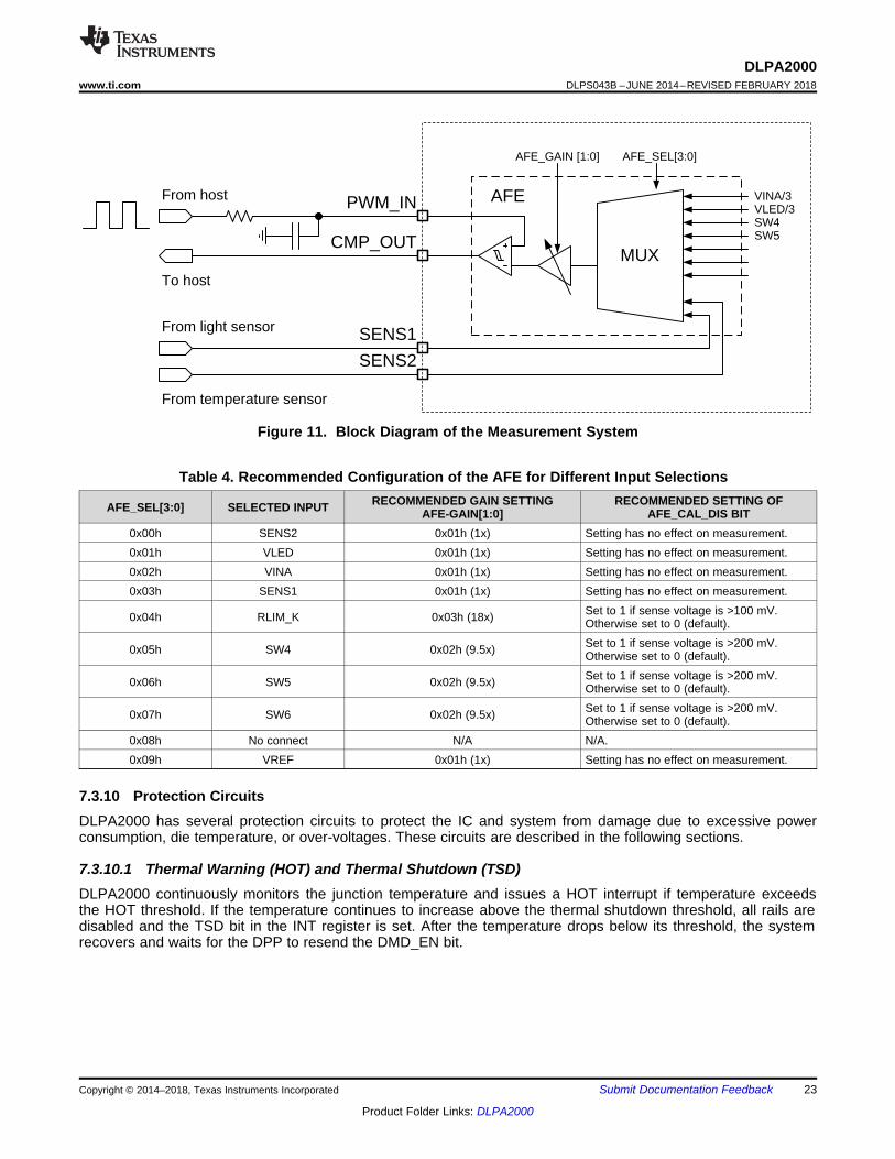
7.3.9 Measurement SystemThe measurement system is composed of a 10:1 analog multiplexer (MUX), a programmable-gain amplifier, anda comparator. It works together with the DPP processor to provide:• White-point correction (WPC) by independently adjusting the RGB LED currents after measuring the
brightness of each color with an external light sensor• A measurement of the:
– Battery voltage– LED forward voltage– Exact LED current– Temperature as derived by measuring the voltage across an external thermistor
Figure 11 shows a block diagram of the measurement system.
From light sensor
From host
From temperature sensor
To host
SW4SW5
SENS1
VINA/3VLED/3
SENS2
CMP_OUT
PWM_IN
AFE_SEL[3:0]AFE_GAIN [1:0]
AFE
MUX
23
DLPA2000www.ti.com DLPS043B –JUNE 2014–REVISED FEBRUARY 2018
Product Folder Links: DLPA2000
Submit Documentation FeedbackCopyright © 2014–2018, Texas Instruments Incorporated
Figure 11. Block Diagram of the Measurement System
Table 4. Recommended Configuration of the AFE for Different Input Selections
AFE_SEL[3:0] SELECTED INPUT RECOMMENDED GAIN SETTINGAFE-GAIN[1:0]
RECOMMENDED SETTING OFAFE_CAL_DIS BIT
0x00h SENS2 0x01h (1x) Setting has no effect on measurement.0x01h VLED 0x01h (1x) Setting has no effect on measurement.0x02h VINA 0x01h (1x) Setting has no effect on measurement.0x03h SENS1 0x01h (1x) Setting has no effect on measurement.
0x04h RLIM_K 0x03h (18x) Set to 1 if sense voltage is >100 mV.Otherwise set to 0 (default).
0x05h SW4 0x02h (9.5x) Set to 1 if sense voltage is >200 mV.Otherwise set to 0 (default).
0x06h SW5 0x02h (9.5x) Set to 1 if sense voltage is >200 mV.Otherwise set to 0 (default).
0x07h SW6 0x02h (9.5x) Set to 1 if sense voltage is >200 mV.Otherwise set to 0 (default).
0x08h No connect N/A N/A.0x09h VREF 0x01h (1x) Setting has no effect on measurement.
7.3.10 Protection CircuitsDLPA2000 has several protection circuits to protect the IC and system from damage due to excessive powerconsumption, die temperature, or over-voltages. These circuits are described in the following sections.
7.3.10.1 Thermal Warning (HOT) and Thermal Shutdown (TSD)DLPA2000 continuously monitors the junction temperature and issues a HOT interrupt if temperature exceedsthe HOT threshold. If the temperature continues to increase above the thermal shutdown threshold, all rails aredisabled and the TSD bit in the INT register is set. After the temperature drops below its threshold, the systemrecovers and waits for the DPP to resend the DMD_EN bit.

Thermal Shutdown
Threshold
Thermal warning
Threshold
HOT
(Internal Signal)
Available Time for Controlled
Shutdown of System
Temperature
TSD
(Internal Signal)
Hysteresis
Hysteresis
24
DLPA2000DLPS043B –JUNE 2014–REVISED FEBRUARY 2018 www.ti.com
Product Folder Links: DLPA2000
Submit Documentation Feedback Copyright © 2014–2018, Texas Instruments Incorporated
Figure 12. Definition of the Thermal Shutdown and Hot-Die Temperature Warning
7.3.10.2 Low Battery Warning (BAT_LOW) and Undervoltage Lockout (UVLO)If the battery voltage drops below the BAT_LOW threshold (typically 3.0 V) the BAT_LOW interrupt is issued, butnormal operation continues. After the battery drops below the undervoltage threshold which has a defaulthardcoded value of 2.3 V (this UVLO voltage can be changed through register 09h from 2.3 V to 4.5 V), theUVLO interrupt is issued, all rails are powered down in sequence, the DMD_EN bit is reset, and the part entersSTANDBY mode. The power rails cannot be re-enabled before the input voltage recovers to >2.4 V. To re-enablethe rails, the PROJ_ON pin must be toggled. The undervoltage threshold is programmable from 2.3 V to 4.5 V in31 steps.
The UVLO shutdown process will protect the DMD by allowing time for the mirrors to park, then doing a fastdischarge of VOFS, VRST, and VBIAS. This protection occurs even in the case of sudden battery removal from theprojector, as long as the bulk capacitance on the battery voltage (VINx) keeps this voltage above 2.3 V for as longas needed for VOFS, VRST, and VBIAS to discharge to the required safe levels as shown in the DMD data sheet.VOFS, VRST, and VBIAS discharge times depend on the load capacitance on each regulator. When for instanceevery supply is decoupled using a capacitor of 0.5 µF, VINx should stay above 2.3 V for at least 100 µs after thebattery is suddenly removed. During this time, the mirrors can be placed in a safe position and VOFS, VRST, andVBIAS can be discharged.
NOTEAs required by the DMD data sheet, LS_OUT must stay above 1.65 V until VOFS, VRST,and VBIAS have discharged to their required safe levels.

Hysteresis
VINA
BAT LOW(Internal Signal)
ACTIVE
INACTIVE
UVLO Threshold
Programmable Deglitch Time1
UVLO
ACTIVE
INACTIVE
BAT_LOW ThresholdHysteresis
200-µsdeglitch
(Internal Signal)
25
DLPA2000www.ti.com DLPS043B –JUNE 2014–REVISED FEBRUARY 2018
Product Folder Links: DLPA2000
Submit Documentation FeedbackCopyright © 2014–2018, Texas Instruments Incorporated
A. This time is programmable from 0 to 100 µs.
Figure 13. UVLO is Asserted When the Input Supply Drops Below the UVLO Threshold
7.3.10.3 DMD Regulator Fault (DMD_FLT)The DMD regulator is continuously monitored to check if the output rails are in regulation and if the inductorcurrent increases as expected during a switching cycle. If either one of the output rails drops out of regulation (forexample, due to a shorted output) or the inductor current does not increase as expected during a switching cycle(due to a disconnected inductor), the DMD_FLT interrupt bit is set in the INT register, the DMD_EN bit is reset,and the DMD regulator is shut down. Resetting the DMD_EN bit also causes the LED driver to power down. Torestart the system, the PROJ_ON pin must be toggled. In case the interrupt is masked, it is sufficient to set theDMD_EN bit to restart the system.
7.3.10.4 V6V Power-Good (V6V_PGF) FaultThe LED driver regulation loop requires the V6V rail for proper operation. The rail is continuously monitored andshould the output drop below the power-good threshold, the V6V_PGF bit is set. The VLED buck-boost is thendisabled and attempts to restart automatically.
7.3.10.5 VLED Overvoltage (VLED_OVP) FaultIf the buck-boost output voltage rises above 5.4 V, the VLED_OVP interrupt is set but the buck-boost regulator isnot turned off. A typical condition to cause this fault is an open LED.
7.3.10.6 VLED Power Save ModeIn normal PWM operation, the efficiency of the VLED buck-boost converter dramatically reduces for LED currentsbelow 100 mA. In this case, the power save mode allows high converting efficiency at low output currents byskipping pulses in the switcher’s gate driver control.
7.3.10.7 V1V8 PG FailureIf for any reason the voltage on the LS_OUT drops below approximately 1.3 V, then VOFS, VBIAS, and VRSTimmediately go into fast shut down. Holding off power down to do mirror parking is not included since 1.3 V is toolow to wait for this. Reactivating can only be done by toggling the PROJ_ON off and on again.
7.3.10.8 Interrupt Pin (INTZ)The interrupt pin is used to signal events and fault conditions to the host processor. Whenever a fault or eventoccurs in the IC, the corresponding interrupt bit is set in the INT register, and the open-drain output is pulled low.The INTZ pin is released (returns to HiZ state) and fault bits are cleared when the INT register is read by thehost.
However, if a failure persists, the corresponding INT bit remains set and the INTZ pin is pulled low again after amaximum of 32 µs.

A6 A5 A4 A3 A2 A1 A0 N7 N6 N5 N4 N3 N2 N1 N0
Byte 0 Byte 1
W/nR
Byte0 Byte1 Byte2 Byte3 ByteN
Data for A[6:0] Data for A[6:0] + 1 Data for A[6:0] + (N – 2)
SPI_CSZ
SPI_DIN
SPI_DOUT
SPI_CLK
Set SPI_CSZ = 1 here to write/read one register location Hold SPI_CSZ = 0 to enable auto-increment mode
Header Register Data (write)
Register Data (read)
Register Address
SPI_DIN
SPI_CLK
W/nR Set high for write, low for read
26
DLPA2000DLPS043B –JUNE 2014–REVISED FEBRUARY 2018 www.ti.com
Product Folder Links: DLPA2000
Submit Documentation Feedback Copyright © 2014–2018, Texas Instruments Incorporated
Interrupt events include fault conditions such as power-good faults, over-voltage, over-temperature shutdown,and UVLO. For all interrupt conditions see the interrupt register on Figure 28.
The MASK register is used to mask events from generating interrupts, that is, from pulling the INTZ pin low. TheMASK settings affect the INTZ pin only and have no impact on protection and monitor circuits themselves. Whenan interrupt is masked, the event causing the interrupt still sets the corresponding bit in the INT register.However, it does not pull the INTZ pin low.
7.3.10.9 SPIDLPA2000 provides a 4-wire SPI port that supports high-speed serial data transfers up to 33.3 MHz. Supportincludes register and data buffer write and read operations. The SPI_CSZ input serves as the active low chipselect for the SPI port. The SPI_CSZ input must be forced low in order to write or read registers and databuffers. When SPI_CSZ is forced high, the data at the SPI_DIN input is ignored, and the SPI_DOUT output isforced to a high-impedance state. The SPI_DIN input serves as the serial data input for the port; the SPI_DOUToutput serves as the serial data output. The SPI_CLK input serves as the serial data clock for both the input andoutput data. Data is latched at the SPI_DIN input on the rising edge of SPI_CLK, while data is clocked out of theSPI_DOUT output on the falling edge of SPI_CLK. Figure 14 shows the SPI port protocol. Byte 0 is referred to asthe command byte, where the most significant bit is the write/not read bit. For the W/nR bit, a 1 indicates a writeoperation, while a 0 indicates a read operation. The remaining seven bits of the command byte are the registeraddress targeted by the write or read operation. The SPI port supports write and read operations for multiplesequential register addresses through the implementation of an auto-increment mode. As shown in Figure 14,the auto-increment mode is invoked by simply holding the SPI_CSZ input low for multiple data bytes. Theregister address is automatically incremented after each data byte transferred, starting with the address specifiedby the command byte. After reaching address 0x7Fh the address pointer jumps back to 0x00h.
Figure 14. SPI Protocol
7.3.11 Password Protected RegistersRegister addresses 0x11h through 0x27h can be read-accessed the same way as any other register, but areprotected against accidental write operations through the PASSWORD register (address 0x10h). To write to aprotected register, follow these steps:1. Write data 0xBAh to register address 0x10h.2. Write data 0xBEh to register address 0x10h.
Both writes must be consecutive, that is, there must be no other read or write operation in between sending thetwo bytes. After the password has been successfully written, registers 0x11h through 0x27h are unlocked andcan be write accessed using the regular SPI protocol. They remain unlocked until any byte other than 0xBAh iswritten to the PASSWORD register or the part is power cycled.
To check if the registers are unlocked, read back the PASSWORD register. If the data returned is 0x00h, theregisters are locked. If the PASSWORD register returns 0x01h, the registers are unlocked.

27
DLPA2000www.ti.com DLPS043B –JUNE 2014–REVISED FEBRUARY 2018
Product Folder Links: DLPA2000
Submit Documentation FeedbackCopyright © 2014–2018, Texas Instruments Incorporated
(1) Settings can be done through Reg01h [9] and Reg2E [119].(2) Power-good faults, over-voltage, overtemperature shutdown, and undervoltage lockout.(3) Settings can be done through Reg47h [60], bit is named VLED_EN_SET.
7.4 Device Functional Modes
Table 5. Modes of OperationMODE DESCRIPTION
OFFThis is the lowest-power mode of operation. All power functions are turned off, registers are reset to their default values, andthe IC does not respond to SPI commands. RESETZ pin is pulled low. The IC will enter OFF mode whenever the PROJ_ONpin is low.
STANDBYThe DMD regulators and LED power (VLED) are turned off, but the IC does respond to the SPI. The device enters STANDBYmode whenever PROJ_ON is set high or DMD_EN (1) bit is set to 0 using the SPI interface after PROJ_ON is already high.The device also enters STANDBY mode when a fault condition is detected (2). (See Protection Circuits).
ACTIVE1 The DMD supplies are enabled but LED power (VLED) is disabled. PROJ_ON pin must be high, DMD_EN bit must be set to 1,and VLED_EN
(3) bit is set to 0.
ACTIVE2 DMD supplies and LED power are enabled. PROJ_ON pin must be high and DMD_EN and VLED_EN bits must both be set to1.
Table 6. Device State as a Function of Control-PinStatus
PROJ_ON PIN STATELOW OFF
HIGH
STANDBYACTIVE1ACTIVE2(Device state depends on DMD_EN and VLED_ENbits and whether there are any fault conditions.)

POWERDOWN
OFF
STANDBY
ACTIVE 1
ACTIVE 2
VLED_EN = 0
&
Valid power source connected
VRST = OFFVBIAS = OFFVOFS = OFFVLED = OFFSPI interface disabledPWR_EN = lowRESETZ = lowAll registers set to default values
DMD_EN = 0|| FAULT = 1
PROJ_ON = low
PROJ_ON = low
PROJ_ON = high
DMD_EN = 1FAULT = 0
VLED_EN = 1
VRST = OFFVBIAS = OFFVOFS = OFFVLED = OFFSPI interface enabledPWR_EN = highRESETZ = high (but is low if entered state due to UVLO detection)
VRST = ONVBIAS = ONVOFS = ONVLED = OFFSPI interface enabledPWR_EN = highRESETZ = high
VRST = ONVBIAS = ONVOFS = ONVLED = ONSPI interface enabledPWR_EN = highRESETZ = high
28
DLPA2000DLPS043B –JUNE 2014–REVISED FEBRUARY 2018 www.ti.com
Product Folder Links: DLPA2000
Submit Documentation Feedback Copyright © 2014–2018, Texas Instruments Incorporated
A. || = OR, & = AND.B. FAULT = Undervoltage on any supply (except LS_OUT), thermal shutdown, or UVLO detection.C. UVLO detection, per the diagram, causes the DLPA2000 to go into the standby state. This is not the lowest power
state. If lower power is desired, PROJ_ON should be set low.D. DMD_EN register bit can be reset or set by SPI writes. DMD_EN defaults to 0 when PROJ_ON goes from low to high
and then the DPP ASIC software automatically sets it to 1. Also, FAULT = 1 causes the DMD_EN register bit to bereset.
E. PWR_EN is a signal internal to the PAD200x. This signal turns on the VCORE regulator and the load switch thatdrives pin LS_OUT.
Figure 15. State Diagram

29
DLPA2000www.ti.com DLPS043B –JUNE 2014–REVISED FEBRUARY 2018
Product Folder Links: DLPA2000
Submit Documentation FeedbackCopyright © 2014–2018, Texas Instruments Incorporated
7.5 Register Maps
Table 7. Register Description
REGISTER ADDRESS(HEX) NAME TABLE DESCRIPTION DEFAULT
USER CONFIGURATION DEFINITIONSR 0x00 CHIP ID Figure 16 Chip revision register; DLPA2000 B3
R/W 0x01 CHIPENABLE Figure 17 Enable register 0FR/W 0x02 IREG Figure 18 Transient-current limit settings 30R/W 0x03 SW4MSB Figure 19 Regulation current MSB, SW4 0R/W 0x04 SW4LSB Table 12, Table 13 Regulation current LSB, SW4 0R/W 0x05 SW5MSB Figure 21 Regulation current MSB, SW5 0R/W 0x06 SW5LSB Figure 22, Table 16 Regulation current LSB, SW5 0R/W 0x07 SW6MSB Figure 23 Regulation current MSB, SW6 0R/W 0x08 SW6LSB Figure 24, Table 19 Regulation current LSB, SW6 0R/W 0x09 SWCNTRL Figure 25 Switch ON/OFF control (direct mode) 0R/W 0x0A AFE Figure 26 AFE (MUX) control 0R/W 0x0B BBM Figure 27, Table 22 Break before make timing 0
R 0x0C INT Figure 28, Table 23 Interrupt register 0R/W 0x0D INT MASK Figure 29, Table 24 Interrupt mask register DFh
R/W 0x0E TIMING Figure 30, Table 26 Timing register VOFS, VBIAS, VRST, andRESETZ 7
R/W 0x0F MOTOR CTRL Figure 31, Table 27 Motor control register 0USER PROTECTED DEFINITION
R/W 0x10 PASSWORD Figure 32 Password register 0R/W 0x11 SYSTEM Figure 33 System configuration register 0
USER EEPROM SCRATCH PAD DEFINITIONR/W 0x20 BYTE0 Figure 34 User EEPROM, Byte0 0R/W 0x21 BYTE1 Figure 35 User EEPROM, Byte1 0R/W 0x22 BYTE2 Figure 36 User EEPROM, Byte2 0R/W 0x23 BYTE3 Figure 37 User EEPROM, Byte3 0R/W 0x24 BYTE4 Figure 38 User EEPROM, Byte4 0R/W 0x25 BYTE5 Figure 39 User EEPROM, Byte5 0R/W 0x26 BYTE6 Figure 40 User EEPROM, Byte6 0R/W 0x27 BYTE7 Figure 41 User EEPROM, Byte7 0
7.5.1 Chip Revision Register
Figure 16. Chip Revision Register, Address = 00h, HEX = B3
7 6 5 4 3 2 1 0CHIP ID [7:0]
R R R R R R R RLEGEND: R/W = Read/Write; R = Read only; -n = value after reset.
Table 8. Chip Revision Register Field DescriptionsBIT FIELD TYPE RESET DESCRIPTION7:4
CHIP IDR 1011 CHIPID<3:0>
3:0 R 0011 REVID<3:0>

30
DLPA2000DLPS043B –JUNE 2014–REVISED FEBRUARY 2018 www.ti.com
Product Folder Links: DLPA2000
Submit Documentation Feedback Copyright © 2014–2018, Texas Instruments Incorporated
7.5.2 Enable Register
Figure 17. Enable Register, Address = 01h, HEX = 0F
7 6 5 4 3 2 1 0CHIPENABLE [15:8]
R/W R/W R/W R/W R/W R/W R/W R/WLEGEND: R/W = Read/Write; R = Read only; -n = value after reset
Table 9. Enable Register Field DescriptionsBIT FIELD TYPE RESET DESCRIPTION
15:12
CHIPENABLE
R/W 0000 USER_GPO<3:0>
11 R/W 1 VLED_POWER_SAVE_MODE_DISPower save mode is used to improve efficiency at light load.
10 R/W 1FAST_SHUTDOWN_ENApplicable only during a fault condition.Shutdown timing is defined by register 0Eh (see Figure 7).
9 R/W 1 DMD_EN8 R/W 1 VLED_EN
7.5.3 Transient-Current Limit Settings
Figure 18. Transient-Current Limit Settings, Address = 02h, HEX = 30
7 6 5 4 3 2 1 0IREG [23:16]
R/W R/W R/W R/W R/W R/W R/W R/WLEGEND: R/W = Read/Write; R = Read only; -n = value after reset.
Table 10. Transient-Current Limit Settings Field DescriptionsBIT FIELD TYPE RESET DESCRIPTION23 RSVD R/W 0 Not used
22:19 IREG R/W 0110
IREG_ILIM<3:0> RLIM = 100 mΩ0000 130 mA0001 150 mA0010 172 mA0011 192 mA0100 220 mA0101 275 mA0110 330 mA0111 440 mA1000 550 mA1001 660 mA1010 770 mA1011 880 mA1100 990 mA1101 1160 mA1110 1330 mA1111 1500 mA
18 SW6LIM_EN R/W 0
SW6LIM_ENTransient current-limit enable for SW60 – Transient current-limit is disabled1 – Transient current-limit is enabled

31
DLPA2000www.ti.com DLPS043B –JUNE 2014–REVISED FEBRUARY 2018
Product Folder Links: DLPA2000
Submit Documentation FeedbackCopyright © 2014–2018, Texas Instruments Incorporated
Table 10. Transient-Current Limit Settings Field Descriptions (continued)BIT FIELD TYPE RESET DESCRIPTION
17 SW5LIM_EN R/W 0
SW5LIM_ENTransient current-limit enable for SW50 – Transient current-limit is disabled1 – Transient current-limit is enabled
16 SW4LIM_EN R/W 0
SW4LIM_ENTransient current-limit enable for SW40 – Transient current-limit is disabled1 – Transient current-limit is enabled
7.5.4 Regulation Current MSB, SW4
Figure 19. Regulation Current MSB, SW4, Address = 03h, HEX = 00
7 6 5 4 3 2 1 0SW4MSB [31:24]
R/W R/W R/W R/W R/W R/W R/W R/WLEGEND: R/W = Read/Write; R = Read only; -n = value after reset.
(1) The DLPA2000 can use up to code 0x0FFh for SW4_IDAC[9:0].
Table 11. Regulation Current MSB, SW4 Field Descriptions (1)
BIT FIELD TYPE RESET DESCRIPTION31:26
SW4MSBR/W 0000 TBD
25:24 R/W 0000 SW4_IDAC<9:8>
7.5.5 Regulation Current LSB, SW4
Figure 20. Regulation Current LSB, SW4, Address = 04h, HEX = 00
7 6 5 4 3 2 1 0SW4LSB [39:32]
R/W R/W R/W R/W R/W R/W R/W R/WLEGEND: R/W = Read/Write; R = Read only; -n = value after reset.
Table 12. Regulation Current LSB, SW4 Field DescriptionsBIT FIELD TYPE RESET DESCRIPTION
39:32 SW4LSB R/W 00000000 SW4_IDAC<7:0>
(1) Values shown are for a typical DLPA2000 unit at T = 25°C. Typical step size is 0.95 mA for RLIM = 100 mΩ.(2) The DLPA2000 can use up to code 0x307h for SW4_IDAC[9:0].
Table 13. Regulation Current LSB, SW4 Bit DefinitionsDLPA2000 (1) (2)
SW4_IDAC[9:0] LED CURRENT SW4_IDAC[9:0] LED CURRENT SW4_IDAC[9:0] LED CURRENT0x000h 0 mA 0x100h 257 mA 0x200h 500 mA0x00Ch 25 mA 0x101h 258 mA 0x201h 501 mA0x00Dh 26 mA 0x102h 259 mA 0x202h 502 mA... ... ... ... ... ...0x0FEh 255 mA 0x1FEh 498 mA 0x306h 749 mA0x0FFh 256 mA 0x1FFh 499 mA 0x307h 750 mA

32
DLPA2000DLPS043B –JUNE 2014–REVISED FEBRUARY 2018 www.ti.com
Product Folder Links: DLPA2000
Submit Documentation Feedback Copyright © 2014–2018, Texas Instruments Incorporated
7.5.6 Regulation Current MSB, SW5
Figure 21. Regulation Current MSB, SW5, Address = 05h, HEX = 00
7 6 5 4 3 2 1 0SW5MSB [47:40]
R/W R/W R/W R/W R/W R/W R/W R/WLEGEND: R/W = Read/Write; R = Read only; -n = value after reset.
(1) The DLPA2000 can use up to code 0x0FFh for SW5_IDAC[9:0].
Table 14. Regulation Current MSB, SW5 Field Descriptions (1)
BIT FIELD TYPE RESET DESCRIPTION47:42
SW5MSBR/W 0000 TBD
41:40 R/W 0000 SW5_IDAC<9:8>
7.5.7 Regulation Current LSB, SW5
Figure 22. Regulation Current LSB, SW5, Address = 06h, HEX = 00
7 6 5 4 3 2 1 0SW5LSB [55:48]
R/W R/W R/W R/W R/W R/W R/W R/WLEGEND: R/W = Read/Write; R = Read only; -n = value after reset.
Table 15. Regulation Current LSB, SW5 Field DescriptionsBIT FIELD TYPE RESET DESCRIPTION
55:48 SW5LSB R/W 00000000 SW5_IDAC<7:0>
(1) Values shown are for a typical DLPA2000 unit at T = 25°C. Typical step size is 0.95 mA for RLIM = 100 mΩ.(2) The DLPA2000 can use up to code 0x307h for SW5_IDAC[9:0].
Table 16. Regulation Current LSB, SW5 Bit DefinitionsDLPA2000 (1) (2)
SW5_IDAC[9:0] LED CURRENT SW5_IDAC[9:0] LED CURRENT SW5_IDAC[9:0] LED CURRENT0x000h 0 mA 0x100h 257 mA 0x200h 500 mA0x00Ch 25 mA 0x101h 258 mA 0x201h 501 mA0x00Dh 26 mA 0x102h 259 mA 0x202h 502 mA... ... ... ... ... ...0x0FEh 255 mA 0x1FEh 498 mA 0x306h 749 mA0x0FFh 256 mA 0x1FFh 499 mA 0x307h 750 mA
33
DLPA2000www.ti.com DLPS043B –JUNE 2014–REVISED FEBRUARY 2018
Product Folder Links: DLPA2000
Submit Documentation FeedbackCopyright © 2014–2018, Texas Instruments Incorporated
7.5.8 Regulation Current MSB, SW6
Figure 23. Regulation Current MSB, SW6, Address = 07h, HEX = 00
7 6 5 4 3 2 1 0SW6MSB [63:56]
R/W R/W R/W R/W R/W R/W R/W R/WLEGEND: R/W = Read/Write; R = Read only; -n = value after reset.
(1) The DLPA2000 can use up to code 0x0FFh for SW6_IDAC[9:0].
Table 17. Regulation Current MSB, SW6 Field Descriptions (1)
BIT FIELD Type Reset Description63:58
SW6MSBR/W 0000 TBD
57:56 R/W 0000 SW6_IDAC<9:8>
7.5.9 Regulation Current LSB, SW6
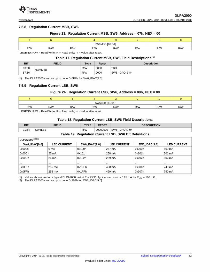
Figure 24. Regulation Current LSB, SW6, Address = 08h, HEX = 00
7 6 5 4 3 2 1 0SW6LSB [71:64]
R/W R/W R/W R/W R/W R/W R/W R/WLEGEND: R/W = Read/Write; R = Read only; -n = value after reset.
Table 18. Regulation Current LSB, SW6 Field DescriptionsBIT FIELD TYPE RESET DESCRIPTION
71:64 SW6LSB R/W 00000000 SW6_IDAC<7:0>
(1) Values shown are for a typical DLPA2000 unit at T = 25°C. Typical step size is 0.95 mA for RLIM = 100 mΩ.(2) The DLPA2000 can use up to code 0x307h for SW6_IDAC[9:0].
Table 19. Regulation Current LSB, SW6 Bit DefinitionsDLPA2000 (1) (2)
SW6_IDAC[9:0] LED CURRENT SW6_IDAC[9:0] LED CURRENT SW6_IDAC[9:0] LED CURRENT0x000h 0 mA 0x100h 257 mA 0x200h 500 mA0x00Ch 25 mA 0x101h 258 mA 0x201h 501 mA0x00Dh 26 mA 0x102h 259 mA 0x202h 502 mA... ... ... ... ... ...0x0FEh 255 mA 0x1FEh 498 mA 0x306h 749 mA0x0FFh 256 mA 0x1FFh 499 mA 0x307h 750 mA
34
DLPA2000DLPS043B –JUNE 2014–REVISED FEBRUARY 2018 www.ti.com
Product Folder Links: DLPA2000
Submit Documentation Feedback Copyright © 2014–2018, Texas Instruments Incorporated
7.5.10 Switch On/Off Control (Direct Mode)
Figure 25. Switch On/Off Control (Direct Mode), Address = 09h, HEX = 00
7 6 5 4 3 2 1 0SWCNTRL [79:72]
R/W R/W R/W R/W R/W R/W R/W R/WLEGEND: R/W = Read/Write; R = Read only; -n = value after reset.
Table 20. Switch On/Off Control (Direct Mode) Field DescriptionsBIT FIELD TYPE RESET DESCRIPTION
79
SWCNTRL
R/W 0 SW6 (controls switch 6 if direct mode(see reg 11h) is enabled)
0000000001.....1111011111
2.3 V (minimum value – default value)2.37 VStep approximately 70 mV4.43 V4.5 V (maximum value)
78 R/W 0 SW5 (controls switch 5 if direct mode(see reg 11h) is enabled)
77 R/W 0 SW4 (controls switch 4 if direct mode(see reg 11h) is enabled)
76:72 R/W 00000 UVLO_TRIM<4:0>
7.5.11 AFE (MUX) Control
Figure 26. AFE (MUX) Control, Address = 0Ah, HEX = 00
7 6 5 4 3 2 1 0AFE [87:80]
R/W R/W R/W R/W R/W R/W R/W R/WLEGEND: R/W = Read/Write; R = Read only; -n = value after reset.
Table 21. AFE (MUX) Control Field DescriptionsBIT FIELD TYPE RESET DESCRIPTION87
AFE
R/W 00 AFE_EN86 R/W 00 AFE_CAL_DIS
85:84 R/W 00 AFE_GAIN<1:0>83:80 R/W 00 AFE_SEL<3:0>
7.5.12 Break Before Make (BBM) Timing
Figure 27. BBM Timing, Address = 0Bh, HEX = 00
7 6 5 4 3 2 1 0BBM [95:88]
R/W R/W R/W R/W R/W R/W R/W R/WLEGEND: R/W = Read/Write; R = Read only; -n = value after reset.
(1) It takes 333 to 444 ns to turn off the switches from the time a change occurs on LED_SEL[1:0].
Table 22. BBM Timing Field Descriptions (1)
BIT FIELD TYPE RESET DESCRIPTION95:88 BBM R/W 00000000 BBM_DELAY<7:0>
0x00 – 0 ns 0x40 – 7326 ns 0x80 – 14430 ns 0xC0 – 21534 ns0x01 – 333 ns 0x41 – 7437 ns 0x81 – 14541 ns 0xC1 – 21645 ns0x02 – 444 ns 0x42 – 7548 ns 0x82 – 14652 ns 0xC2 – 21756 ns... ... ... ...0x3E – 7104 ns 0x7E – 14208 ns 0xBE – 21312 ns 0xFE – 28416 ns0x3F – 7215 ns 0x7F – 14319 ns 0xBF – 21423 ns 0xFF – 28527 ns

35
DLPA2000www.ti.com DLPS043B –JUNE 2014–REVISED FEBRUARY 2018
Product Folder Links: DLPA2000
Submit Documentation FeedbackCopyright © 2014–2018, Texas Instruments Incorporated
7.5.13 Interrupt Register
Figure 28. Interrupt Register, Address = 0Ch, HEX = 00
7 6 5 4 3 2 1 0INT [103:96]
R R R R R R R RLEGEND: R/W = Read/Write; R = Read only; -n = value after reset.
Table 23. Interrupt Register Field DescriptionsBIT FIELD TYPE RESET DESCRIPTION103
INT
R 0
VLED_OVPVLED buck_boost overvoltage fault interrupt (normal operationresumes)0 – No fault1 – Buck_boost output is above OVP threshold
102
R 0
IREG_PG_FAULTV6V power-good fault interrupt (normal operation resumes)0 – No fault1 – V6V is not in regulation
101
R 0
PROJ_ON_INTProj_On interrupt (part enters OFF mode)0 – Pin is pulled high, normal mode1 – Pin is pulled low, alerts the DPP that the DMD regulator isabout to shut down.
100
R 0
DMD_FAULTDMD regulator fault (part enters STANDBY mode and DMD_ENbit is cleared)0 – No fault1 – The inductor current is not increasing at the correct rate,likely to be caused by an open inductor.Or, one of the regulator outputs has dropped below the power-good threshold, likely to be caused by a short.
99
R 0
UVLOUVLO interrupt (sensed at VINA pin), DMD bit is cleared.0 – Battery voltage is above the UVLO threshold.1 – Battery voltage has dropped below the UVLO threshold.
98
R 0
BAT_LOW_WARNLow battery warning interrupt (sensed at VINA pin, normaloperation resumes)0 – Battery voltage is above the low-battery threshold1 – Battery voltage has dropped below the low-battery threshold
97
R 0
TS_WARNThermal warning interrupt (normal operation resumes)0 – Die temperature is in normal operating range1 – Die temperature is above the HOT thresholdOr, part has not cooled down enough to recover from HOT.
96
R 0
TS_WARNThermal Warning Interrupt (normal operation resumes)0 – Die temperature is in normal operating range1 – Die temperature is above the HOT thresholdOr, part has not cooled down enough to recover from HOT.

36
DLPA2000DLPS043B –JUNE 2014–REVISED FEBRUARY 2018 www.ti.com
Product Folder Links: DLPA2000
Submit Documentation Feedback Copyright © 2014–2018, Texas Instruments Incorporated
7.5.14 Interrupt Mask Register
Figure 29. Interrupt Mask Register, Address = 0Dh, HEX = DF
7 6 5 4 3 2 1 0INT MASK [111:104]
R/W R/W R/W R/W R/W R/W R/W R/WLEGEND: R/W = Read/Write; R = Read only; -n = value after reset.
Table 24. Interrupt Mask Register Field DescriptionsBIT FIELD TYPE RESET DESCRIPTION111
INT MASK
R/W 1 VLED BUCK_BOOSTOvervoltage fault interrupt mask0 – Interrupt is not masked1 – Interrupt is masked
110 R/W 1 IREG_PG_FAULT_MASK0 – Interrupt is not masked1 – Interrupt is masked
109 R/W 0 PROJ_ON interrupt mask0 – Interrupt is not masked1 – Interrupt is masked
108 R/W 1 DMD_REGULATOR fault mask0 – Interrupt is not masked1 – Interrupt is masked
107 R/W 1 UVLO_MASK0 – Interrupt is not masked1 – Interrupt is masked
106 R/W 1 Low battery warning mask (sensed at VINA pin)0 – Interrupt is not masked1 – Interrupt is masked
105 R/W 1 Thermal shutdown interrupt mask0 – Interrupt is not masked1 – Interrupt is masked
104 R/W 1 Thermal warning interrupt mask0 – Interrupt is not masked1 – Interrupt is masked

37
DLPA2000www.ti.com DLPS043B –JUNE 2014–REVISED FEBRUARY 2018
Product Folder Links: DLPA2000
Submit Documentation FeedbackCopyright © 2014–2018, Texas Instruments Incorporated
7.5.15 Timing Register VOFS, VBIAS, VRST, and RESETZ
Figure 30. Timing Register VOFS, VBIAS, VRST, and RESETZ, Address = 0Eh, HEX = 07
7 6 5 4 3 2 1 0TIMING [119:112]
R/W R/W R/W R/W R/W R/W R/W R/WLEGEND: R/W = Read/Write; R = Read only; -n = value after reset.
Table 25. Timing Register VOFS, VBIAS, VRST, and RESETZ Field DescriptionsBIT FIELD TYPE RESET DESCRIPTION
119:116
TIMING
R/W 0000 VOFS/RESETZ_DELAY<3:0> (for values see minimum andmaximum delay)
115:112 R/W 0111 VBIAS/VRST_DELAY<3:0> (for values see minimum andmaximum delay)
Table 26. Timing Register VOFS, VBIAS, VRST, and RESETZ Bit DefinitionsFIELD NAME BIT BIT DEFINITION
TIMING [119:112]
Minimum Delay (μs) Maximum Delay (μs)0000 4.0 4.40001 8.0 8.90010 16.0 17.80011 32.0 35.50100 64.0 71.10101 128.0 142.20110 256.0 284.40111 512.0 569.01000 6.2 7.11001 12.4 14.21010 24.9 28.41011 49.8 56.91100 99.5 113.81101 199.1 227.61110 398.3 455.21111 1024.2 1138.0

38
DLPA2000DLPS043B –JUNE 2014–REVISED FEBRUARY 2018 www.ti.com
Product Folder Links: DLPA2000
Submit Documentation Feedback Copyright © 2014–2018, Texas Instruments Incorporated
7.5.16 Motor Control Register
(1) VINM can be left floating if the motor controller is not used.
Figure 31. Motor Control Register, Address = 0Fh, HEX = 00 (1)
7 6 5 4 3 2 1 0MOTOR CTRL [127:120]
R/W R/W R/W R/W R/W R/W R/W R/WLEGEND: R/W = Read/Write; R = Read only; -n = value after reset.
Table 27. Motor Control Register Field DescriptionsBIT FIELD TYPE RESET DESCRIPTION127
MOTOR CTRL
R/W 0 TBD126 R/W 0 TBD125 R/W 0 MD_EN124 R/W 0 MD_MODE123 R/W 0 MD_AIN1122 R/W 0 MD_AIN2121 R/W 0 MD_BIN1120 R/W 0 MD_BIN2
7.5.17 Password Register
Figure 32. Password Register, Address = 10h, HEX = 00
7 6 5 4 3 2 1 0PASSWORD [135:128]
R/W R/W R/W R/W R/W R/W R/W R/WLEGEND: R/W = Read/Write; R = Read only; -n = value after reset
Table 28. Password Register Field DescriptionsBIT FIELD TYPE RESET DESCRIPTION
135:128 PASSWORD R/W 00000000 USER PASSWORD (0xBAh + 0xBEh) disable (0x00h).Once set, register 11h can be written.
7.5.18 System Configuration Register
Figure 33. System Configuration Register, Address = 11h, HEX = 00
7 6 5 4 3 2 1 0SYSTEM [143:136]
R/W R/W R/W R/W R/W R/W R/W R/WLEGEND: R/W = Read/Write; R = Read only; -n = value after reset.
Table 29. System Configuration Register Field DescriptionsBIT FIELD TYPE RESET DESCRIPTION
143:139
SYSTEM
R/W 00000 TBD138 R/W 0 EEPROM_PROGRAM
Program scratch pad values to EEPROM137 R/W 0 DIRECT_MODE
Allows direct control of switches through SW CONTROLREGISTER
136 R/W 0 TBD

39
DLPA2000www.ti.com DLPS043B –JUNE 2014–REVISED FEBRUARY 2018
Product Folder Links: DLPA2000
Submit Documentation FeedbackCopyright © 2014–2018, Texas Instruments Incorporated
7.5.19 User EEPROM, BYTE0
Figure 34. User EEPROM, BYTE0, Address = 20h, HEX = 00
7 6 5 4 3 2 1 0BYTE0 [7:0]
R/W R/W R/W R/W R/W R/W R/W R/WLEGEND: R/W = Read/Write; R = Read only; -n = value after reset.
Table 30. User EEPROM, BYTE0 Field DescriptionsBIT FIELD TYPE RESET DESCRIPTION7:0 BYTE0 R/W 00000000 USER BYTE 0
7.5.20 User EEPROM, BYTE1
Figure 35. User EEPROM, BYTE1, Address = 21h, HEX = 00
7 6 5 4 3 2 1 0BYTE1 [15:8]
R/W R/W R/W R/W R/W R/W R/W R/WLEGEND: R/W = Read/Write; R = Read only; -n = value after reset.
Table 31. User EEPROM, BYTE1 Field DescriptionsBIT FIELD TYPE RESET DESCRIPTION15:8 BYTE1 R/W 00000000 USER BYTE 1
7.5.21 User EEPROM, BYTE2
Figure 36. User EEPROM, BYTE2, Address = 22h, HEX = 00
7 6 5 4 3 2 1 0BYTE2 [23:16]
R/W R/W R/W R/W R/W R/W R/W R/WLEGEND: R/W = Read/Write; R = Read only; -n = value after reset.
Table 32. User EEPROM, BYTE2 Field DescriptionsBIT FIELD TYPE RESET DESCRIPTION
23:16 BYTE2 R/W 00000000 USER BYTE 2
7.5.22 User EEPROM, BYTE3
Figure 37. User EEPROM, BYTE3, Address = 23h, HEX = 00
7 6 5 4 3 2 1 0BYTE3 [31:24]
R/W R/W R/W R/W R/W R/W R/W R/WLEGEND: R/W = Read/Write; R = Read only; -n = value after reset.
Table 33. User EEPROM, BYTE3 Field DescriptionsBIT FIELD TYPE RESET DESCRIPTION
31:24 BYTE3 R/W 00000000 USER BYTE 3

40
DLPA2000DLPS043B –JUNE 2014–REVISED FEBRUARY 2018 www.ti.com
Product Folder Links: DLPA2000
Submit Documentation Feedback Copyright © 2014–2018, Texas Instruments Incorporated
7.5.23 User EEPROM, BYTE4
Figure 38. User EEPROM, BYTE4, Address = 24h, HEX = 00
7 6 5 4 3 2 1 0BYTE4 [39:32]
R/W R/W R/W R/W R/W R/W R/W R/WLEGEND: R/W = Read/Write; R = Read only; -n = value after reset.
Table 34. User EEPROM, BYTE4 Field DescriptionsBIT FIELD TYPE RESET DESCRIPTION
39:32 BYTE4 R/W 00000000 USER BYTE 4
7.5.24 User EEPROM, BYTE5
Figure 39. User EEPROM, BYTE5, Address = 25h, HEX = 00
7 6 5 4 3 2 1 0BYTE5 [47:40]
R/W R/W R/W R/W R/W R/W R/W R/WLEGEND: R/W = Read/Write; R = Read only; -n = value after reset.
Table 35. User EEPROM, BYTE5 Field DescriptionsBIT FIELD TYPE RESET DESCRIPTION
47:40 BYTE5 R/W 00000000 USER BYTE 5
7.5.25 User EEPROM, BYTE6
Figure 40. User EEPROM, BYTE6, Address = 26h, HEX = 00
7 6 5 4 3 2 1 0BYTE6 [55:48]
R/W R/W R/W R/W R/W R/W R/W R/WLEGEND: R/W = Read/Write; R = Read only; -n = value after reset.
Table 36. User EEPROM, BYTE6 Field DescriptionsBIT FIELD TYPE RESET DESCRIPTION
55:48 BYTE6 R/W 00000000 USER BYTE 6
7.5.26 User EEPROM, BYTE7
Figure 41. User EEPROM, BYTE7, Address = 27h, HEX = 00
7 6 5 4 3 2 1 0BYTE7 [63:56]
R R R R R R R RLEGEND: R/W = Read/Write; R = Read only; -n = value after reset.
Table 37. User EEPROM, BYTE7 Field DescriptionsBIT FIELD TYPE RESET DESCRIPTION
63:56 BYTE7 R 00000000 USER BYTE 7

DC Supplies
BAT+ ±
1.1 V
WVGADDR DMD
DLP2010(WVGADMD)
Included in DLP® Chip Set
1.8 V
2.3 to 5.5 V Projector Module Electronics
DLPA2000
PARKZ
1.1 V
1.8 V
VCORE
VIO
IlluminationOptics
3BIAS, RST, OFS
Thermistor
Parallel I/F
VCC_INTF
EEPROM
DLPC3430/DLPC3435
VCC_FLSH
SPI_1
I2C_1
1.8 VOtherSupplies
1.1 VReg
Cal data (optional)
FLASH, SDRAM
Keypad
Front-EndChip- OSD- AutoLock - Scaler-MicroController
HDMI Receiver
Triple ADC
ChargerDC_IN
VDD
On/Off
HDMI
VGA
SD Card Reader, and
so forth(optional)
FLASH
L1
Spare R/W GPIO
TVP5151 Video
Decoder
BT.656
KeystoneSensor
GPIO_8 (Normal Park)
1.8 V VSPI
SPI_0
eDRAM
L2
L3
GND
CVBS
RESETZINTZ
LED_SEL(2)
CMP_PWM
VLED
WPC
LABB
4
4
PROJ_ONPROJ_ON
1.8 V
SYSPWR
REDGREEN
BLUE
Sub-LVDS DATA
CTRL
I2C
28
HOST_IRQ
CurrentSense
18
CMP_OUT
41
DLPA2000www.ti.com DLPS043B –JUNE 2014–REVISED FEBRUARY 2018
Product Folder Links: DLPA2000
Submit Documentation FeedbackCopyright © 2014–2018, Texas Instruments Incorporated
8 Application and Implementation
NOTEInformation in the following applications sections is not part of the TI componentspecification, and TI does not warrant its accuracy or completeness. TI’s customers areresponsible for determining suitability of components for their purposes. Customers shouldvalidate and test their design implementation to confirm system functionality.
8.1 Application InformationA DLPC343x controller can be used with a DLP2010 (0.2 WVGA) DMD or DLP3010 (0.3 720p) DMD to provide acompact, reliable, high-efficiency display solution for many different video display applications. The DMDs arespatial light modulators which reflect incoming light from an illumination source to one of two directions with theprimary direction being into collection optics within a projection lens. The projection lens sends the light to thedestination needed for the application. Each application is derived primarily from the optical architecture of thesystem and the format of the pixel data being input into the DLPC343x.
In display applications using the DLP2010 DMD or DLP3010 DMD, the DLPA2000 provides all needed analogfunctions including the analog power supplies and the RGB LED driver to provide a robust and efficient displaysolution. Display applications of interest include pico-projectors embedded in display devices like smart phones,tablets, cameras, and camcorders. Other applications include wearable (near-eye) displays, battery-poweredmobile accessories, interactive displays, low latency gaming displays, and digital signage.
Alternately, a DLPC150 controller can be used with a DLP2010 or DLP2010NIR DMD. Applications of interestwhen using the DLPC150 controller include machine vision systems, spectrometers, skin analysis, medicalsystems, material identification, chemical sensing, infrared projection, and compressive sensing. In aspectroscopy application the DLPC150 controller and DLP2010NIR DMD are often combined with a singleelement detector to replace expensive InGaAs array-based detector designs. In this application the DMD acts asa wavelength selector reflecting specific wavelengths of light into the single point detector.
8.2 Typical Projector ApplicationA common application when using DLPA2000 with DLP2010 DMD and DLPC3430 controller is for creating apico-projector embedded in a handheld product. For example, a pico-projector may be embedded in a smartphone, a tablet, a camera, or camcorder. The DLPC3430 in the pico-projector embedded module typicallyreceives images from a host processor within the product as shown in Figure 42. DLPA2000 provides powersupply sequencing and controls the LED currents as required by the application.
Figure 42. Typical Embedded Setup Using DLPA2000

42
DLPA2000DLPS043B –JUNE 2014–REVISED FEBRUARY 2018 www.ti.com
Product Folder Links: DLPA2000
Submit Documentation Feedback Copyright © 2014–2018, Texas Instruments Incorporated
Typical Projector Application (continued)8.2.1 Design RequirementsA pico-projector is created by using a DLP chipset comprised of DLP2010 (0.2 WVGA) DMD, DLPC3430, orDLPC3435 controller and DLPA2000 PMIC/LED driver. The DLPC3430 or DLPC3435 does the digital imageprocessing, the DLPA2000 provides the needed analog functions for the projector, and DMD is the displaydevice for producing the projected image.
In addition to the three DLP chips in the chipset, other chips may be needed. At a minimum, a flash part isneeded to store the software and firmware to control the DLPC3430 or DLPC3435.
The illumination light that is applied to the DMD is typically from red, green, and blue LEDs. These are oftencontained in three separate packages, but sometimes more than one color of LED die may be in the samepackage to reduce the overall size of the pico-projector.
When connecting the DLPC3430 or DLPC3435 to the host processing to receive images, a parallel interface isused. While using the parallel interface, I2C should be connected to the host processor for sending commands tothe DLPC3430 or DLPC3435.
The only power supplies needed external to the projector are the battery (SYSPWR) and a regulated 1.8-Vsupply. The entire pico-projector can be turned on and off by using a single signal called PROJ_ON. WhenPROJ_ON is high, the projector turns on and begins displaying images. When PROJ_ON is set low, the projectorturns off and draws just microamps of current on SYSPWR. When PROJ_ON is set low, the 1.8-V supply cancontinue to be left at 1.8 V and used by other non-projector sections of the product. If PROJ_ON is low, theDLPA2000 will not draw current on the 1.8-V supply.
8.2.2 Detailed Design ProcedureFor connecting together the DLP2010, DLPC3430 or DLPC3435, and DLPA2000, see the reference designschematic. When a circuit board layout is created from this schematic, a very small circuit board is possible. Anexample small board layout is included in the reference design database. Layout guidelines should be followed toachieve a reliable projector.
The optical engine that has the LED packages and the DMD mounted to it is typically supplied by an opticalOEM who specializes in designing optics for DLP projectors.
A miniature stepper motor can optionally be added to the optical engine for creating a motorized focus. Directcontrol and driving of the motor can be done by the DLPA2000, and software commands sent over I2C to theDLPC3430 or DLPC3435 are available to move the motor to the desired position.

Current (mA)
Lum
inan
ce
0 100 200 300 400 500 600 7000
0.1
0.2
0.3
0.4
0.5
0.6
0.7
0.8
0.9
1
D001
43
DLPA2000www.ti.com DLPS043B –JUNE 2014–REVISED FEBRUARY 2018
Product Folder Links: DLPA2000
Submit Documentation FeedbackCopyright © 2014–2018, Texas Instruments Incorporated
Typical Projector Application (continued)8.2.3 Application CurveAs the LED currents that are driven time-sequentially through the red, green, and blue LEDs are increased, thebrightness of the projector increases. This increase is somewhat non-linear, and the curve for typical whitescreen lumens changes with LED currents is as shown in Figure 43. For the LED currents shown, it is assumedthat the same current amplitude is applied to the red, green, and blue LEDs.
SPACE
Figure 43. Luminance vs Current
8.3 Typical Mobile Sensing ApplicationA typical embedded system application using the DLPC150 controller and the DLPC2010NIR is shown inFigure 44. In this configuration, the DLPC150 controller supports a 24-bit parallel RGB input, typical of LCDinterfaces, from an external source or processor. The DLPC150 controller processes the digital input image andconverts the data into the format needed by the DLP2010NIR. The DLP2010NIR steers light by setting specificmicromirrors to the on position, directing light to the detector, while unwanted micromirrors are set to the offposition, directing light away from the detector. The microprocessor sends binary images to the DLP2010NIR tosteer specific wavelengths of light into the detector. The microprocessor uses an analog-to-digital converter tosample the signal received by the detector into a digital value. By sequentially selecting different wavelengths oflight and capturing the values at the detector, the microprocessor can then plot a spectral response to the light.

!"#$%&
'()(*$+$),
-.-&/
0/12
334&3'3
35!67-7894:0/123'3;
35!<&=>?@&A$,
-.BA&/
6.C&,"&D.D&/
!"#$%&&&
'()
!"#$%&&*
!24EF
-.-&/
-.BA&/
/=G4H
/9G
!%"I$J,?")&G@,?JK
CL92AM&4ANM&GOA
N>$%+?K,"%
/==P98NO
!"#+,*&
/==PO5AQ
A!9P-
-.B&/
G,>$%AR@@S?$K
-.-T/
4$*
O52AQM&
A342'
E$U@(V
-./('0('/122'(
23=
=>(%*$%3=P98
/33
G)WGXX
O52AQ
!4GYPG8
5AP98
A!9P7&Z&
&Z&
5H3PAH5:6;
4HAHNF
='!P!0'
='!PG[N
98NF
AR\T5/3A&32N2
5!A34&=N45
!4GYPG8
A]A!04
-.B&/
!4GYPG8
QGANP94^
!(%(SS$S&41L&9WO&:6B;
96=
L2N_ `
/98
N491P98
N491PG[N&:6;
$!+)3)$405.61(
A3&
=(%V
LSR$,"",>
[AL
9SSR+?)(,?")&G@,?JK
3$,$J,"%
=R%%$),A$)K$
/5H3
4H3
894&3$,$J,"%
44
DLPA2000DLPS043B –JUNE 2014–REVISED FEBRUARY 2018 www.ti.com
Product Folder Links: DLPA2000
Submit Documentation Feedback Copyright © 2014–2018, Texas Instruments Incorporated
Typical Mobile Sensing Application (continued)
Figure 44. Typical Application Diagram
8.3.1 Design RequirementsAll applications using the DLP 0.2-inch WVGA chipset require the:• DLPC150 controller, and• DLPA2000 PMIC, and• DLP2010 or DLP2010NIR DMDcomponents for operation. The system also requires an external parallel flash memory device loaded with theDLPC150 configuration and support firmware. DLPC150 does the digital image processing and formats the datafor the DMD. DLPA2000 PMIC provides the needed analog functions for the DLPC150 and DLP2010 orDLP2010NIR. The chipset has several system interfaces and requires some support circuitry. The followinginterfaces and support circuitry are required:
• DLPC150 system interfaces:– Control interface– Trigger interface– Input data interface– Illumination interface
• DLPC150 support circuitry and interfaces:– Reference clock– PLL– Program memory flash interface
• DMD interfaces:– DLPC150 to DMD digital data– DLPC150 to DMD control interface– DLPC150 to DMD micromirror reset control interface

45
DLPA2000www.ti.com DLPS043B –JUNE 2014–REVISED FEBRUARY 2018
Product Folder Links: DLPA2000
Submit Documentation FeedbackCopyright © 2014–2018, Texas Instruments Incorporated
Typical Mobile Sensing Application (continued)8.3.2 Detailed Design Procedure
8.3.2.1 Dlpc150 System InterfacesThe 0.2-inch WVGA chipset supports a 16-bit or 24-bit parallel RGB interface for image data transfers fromanother device. There are two primary output interfaces: Illumination driver control interface and sync outputs.
8.3.2.1.1 Control Interface
The 0.2-inch WVGA chipset supports I2C commands through the control interface. The control interface allowsanother master processor to send commands to the DLPC150 controller to query system status or performrealtime operations, such as LED driver current settings.
8.3.3 Application CurveIn a reflective spectroscopy application, a broadband light source illuminates a sample and the reflected lightspectrum is dispersed onto the DLP2010NIR. A microprocessor in conjunction with the DLPC150 controlsindividual DLP2010NIR micromirrors to reflect specific wavelengths of light to a single point detector. Themicroprocessor uses an analog-to-digital converter to sample the signal received by the detector into a digitalvalue. By sequentially selecting different wavelengths of light and capturing the values at the detector, themicroprocessor can then plot a spectral response to the light. This systems allows the measurement of thecollected light and derive the wavelengths absorbed by the sample. This process leads to the absorptionspectrum shown in Figure 45.
Figure 45. Sample DLPC150 Based Spectrometer Output

46
DLPA2000DLPS043B –JUNE 2014–REVISED FEBRUARY 2018 www.ti.com
Product Folder Links: DLPA2000
Submit Documentation Feedback Copyright © 2014–2018, Texas Instruments Incorporated
9 Power Supply RecommendationsThe DLPA2000 is designed to operate from a 2.3-V to 6-V input voltage supply or battery. To avoid insufficientsupply current due to line drop, ringing due to trace inductance at the VIN terminal, or supply peak currentlimitations, additional bulk capacitance may be required. In the case ringing that is caused by the interaction withthe ceramic input capacitors, an electrolytic or tantalum type capacitor may be needed for damping. The amountof bulk capacitance required should be evaluated such that the input voltage can remain in specification longenough for a proper fast shutdown to occur for the VOFS, VRST, and VBIAS supplies. The shutdown begins whenthe input voltage drops below the programmable UVLO threshold such as when the external power supply orbattery supply is suddenly removed from the system.

47
DLPA2000www.ti.com DLPS043B –JUNE 2014–REVISED FEBRUARY 2018
Product Folder Links: DLPA2000
Submit Documentation FeedbackCopyright © 2014–2018, Texas Instruments Incorporated
10 Layout
10.1 Layout GuidelinesAs for all chips with switching power supplies, the layout is an important step in the design, especially in the caseof high peak currents and high switching frequencies. If the layout is not carefully done, the regulators couldshow stability problems as well as EMI problems. Therefore, use wide and short traces for the main current pathsand for the power ground tracks. Input capacitors, output capacitors, and inductors should be placed as close aspossible to the IC.
Figure 46 shows an example layout that has critical parts placed as close as possible to the pins they areconnected to. Here are recommendations for the following components:
R1 is RLIM and is connected via a wide trace and as short as possible to the DLPA2000 and the ground.L1 is the big inductor for the VLED that is connected via two wide traces to the pins.C3/C4 are the decoupling capacitors for the VLED and they are as close as possible placed to the part and
directly connected to ground.L3/C20 are components used for the VCORE BUCK. L3 is placed close to the pin and connected with a wide
trace to the part. C20 is placed directly beside the inductor and connected to the PGND pin.L2 This inductor is part of the DMD reset regulators and is also placed as close as possible to the
DLPA2000 using wide PCB traces.

48
DLPA2000DLPS043B –JUNE 2014–REVISED FEBRUARY 2018 www.ti.com
Product Folder Links: DLPA2000
Submit Documentation Feedback Copyright © 2014–2018, Texas Instruments Incorporated
10.2 Layout Example
Figure 46. Example Layout of DLPA2000
TI = TI LETTERSYM = YEAR / MONTH DATE CODE LLLL= LOT TRACE CODE S = ASSEMBLY SITE CODE
=pin 1 Marking
TI Y
MLL
LLS
PA
D20
00A
3
49
DLPA2000www.ti.com DLPS043B –JUNE 2014–REVISED FEBRUARY 2018
Product Folder Links: DLPA2000
Submit Documentation FeedbackCopyright © 2014–2018, Texas Instruments Incorporated
11 Device and Documentation Support
11.1 Device Support
11.1.1 Device Nomenclature
Figure 47. DLPA2000 Package Marking(Top View)
11.2 Related LinksThe table below lists quick access links. Categories include technical documents, support and communityresources, tools and software, and quick access to sample or buy.
Table 38. Related Links
PARTS PRODUCT FOLDER SAMPLE & BUY TECHNICALDOCUMENTS
TOOLS &SOFTWARE
SUPPORT &COMMUNITY
DLPA2000 Click here Click here Click here Click here Click hereDLPC3430 Click here Click here Click here Click here Click hereDLPC3435 Click here Click here Click here Click here Click hereDLP2010 Click here Click here Click here Click here Click here
11.3 Community ResourcesThe following links connect to TI community resources. Linked contents are provided "AS IS" by the respectivecontributors. They do not constitute TI specifications and do not necessarily reflect TI's views; see TI's Terms ofUse.
TI E2E™ Online Community TI's Engineer-to-Engineer (E2E) Community. Created to foster collaborationamong engineers. At e2e.ti.com, you can ask questions, share knowledge, explore ideas and helpsolve problems with fellow engineers.
Design Support TI's Design Support Quickly find helpful E2E forums along with design support tools andcontact information for technical support.
11.4 TrademarksDLP, E2E are trademarks of Texas Instruments.All other trademarks are the property of their respective owners.

50
DLPA2000DLPS043B –JUNE 2014–REVISED FEBRUARY 2018 www.ti.com
Product Folder Links: DLPA2000
Submit Documentation Feedback Copyright © 2014–2018, Texas Instruments Incorporated
11.5 Electrostatic Discharge CautionThese devices have limited built-in ESD protection. The leads should be shorted together or the device placed in conductive foamduring storage or handling to prevent electrostatic damage to the MOS gates.
11.6 GlossarySLYZ022 — TI Glossary.
This glossary lists and explains terms, acronyms, and definitions.

51
DLPA2000www.ti.com DLPS043B –JUNE 2014–REVISED FEBRUARY 2018
Product Folder Links: DLPA2000
Submit Documentation FeedbackCopyright © 2014–2018, Texas Instruments Incorporated
12 Mechanical, Packaging, and Orderable InformationThe following pages include mechanical, packaging, and orderable information. This information is the mostcurrent data available for the designated devices. This data is subject to change without notice and revision ofthis document. For browser-based versions of this data sheet, refer to the left-hand navigation.• Insertion of device –The device is located such as symbolization in upper side and lead pins in lower side.• Cover tape – The cover tape does not cover the index hole and does not shift to outside from carrier tape.• Tape Structure –The carrier tape is made of plastic and the structure is shown in above schematic. The
device is put on embossed area of carrier tape, and covered by cover tape made of plastic.• ESD Countermeasure Plastic – material used in both carrier tape and cover tape are static dissipative.• Material – Polycarbonate, Polystyrene or and approved equivalent (Static Dissipative / Antistatic).• Packing method – The reel is packed into Moisture Barrier bag and fastened by heat-sealing after fixed the
end of leader tape by tape. The QFN device packing includes desiccant, humidity indicator.• Reel Box – Each Moisture Barrier bag is packed into reel box.
• Reel Box Material – Corrugated Fiberboard• Shipping Box –The filler such as cushion is added if space exists inside. The size of shipping box will be
changed per packing quantity of reel box.

PACKAGE OPTION ADDENDUM
www.ti.com 16-Feb-2018
Addendum-Page 1
PACKAGING INFORMATION
Orderable Device Status(1)
Package Type PackageDrawing
Pins PackageQty
Eco Plan(2)
Lead/Ball Finish(6)
MSL Peak Temp(3)
Op Temp (°C) Device Marking(4/5)
Samples
DLPA2000DYFFR ACTIVE DSBGA YFF 56 3000 Green (RoHS& no Sb/Br)
SNAGCU Level-1-260C-UNLIM PAD2000A3
(1) The marketing status values are defined as follows:ACTIVE: Product device recommended for new designs.LIFEBUY: TI has announced that the device will be discontinued, and a lifetime-buy period is in effect.NRND: Not recommended for new designs. Device is in production to support existing customers, but TI does not recommend using this part in a new design.PREVIEW: Device has been announced but is not in production. Samples may or may not be available.OBSOLETE: TI has discontinued the production of the device.
(2) RoHS: TI defines "RoHS" to mean semiconductor products that are compliant with the current EU RoHS requirements for all 10 RoHS substances, including the requirement that RoHS substancedo not exceed 0.1% by weight in homogeneous materials. Where designed to be soldered at high temperatures, "RoHS" products are suitable for use in specified lead-free processes. TI mayreference these types of products as "Pb-Free".RoHS Exempt: TI defines "RoHS Exempt" to mean products that contain lead but are compliant with EU RoHS pursuant to a specific EU RoHS exemption.Green: TI defines "Green" to mean the content of Chlorine (Cl) and Bromine (Br) based flame retardants meet JS709B low halogen requirements of <=1000ppm threshold. Antimony trioxide basedflame retardants must also meet the <=1000ppm threshold requirement.
(3) MSL, Peak Temp. - The Moisture Sensitivity Level rating according to the JEDEC industry standard classifications, and peak solder temperature.
(4) There may be additional marking, which relates to the logo, the lot trace code information, or the environmental category on the device.
(5) Multiple Device Markings will be inside parentheses. Only one Device Marking contained in parentheses and separated by a "~" will appear on a device. If a line is indented then it is a continuationof the previous line and the two combined represent the entire Device Marking for that device.
(6) Lead/Ball Finish - Orderable Devices may have multiple material finish options. Finish options are separated by a vertical ruled line. Lead/Ball Finish values may wrap to two lines if the finishvalue exceeds the maximum column width.
Important Information and Disclaimer:The information provided on this page represents TI's knowledge and belief as of the date that it is provided. TI bases its knowledge and belief on informationprovided by third parties, and makes no representation or warranty as to the accuracy of such information. Efforts are underway to better integrate information from third parties. TI has taken andcontinues to take reasonable steps to provide representative and accurate information but may not have conducted destructive testing or chemical analysis on incoming materials and chemicals.TI and TI suppliers consider certain information to be proprietary, and thus CAS numbers and other limited information may not be available for release.
In no event shall TI's liability arising out of such information exceed the total purchase price of the TI part(s) at issue in this document sold by TI to Customer on an annual basis.

TAPE AND REEL INFORMATION
*All dimensions are nominal
Device PackageType
PackageDrawing
Pins SPQ ReelDiameter
(mm)
ReelWidth
W1 (mm)
A0(mm)
B0(mm)
K0(mm)
P1(mm)
W(mm)
Pin1Quadrant
DLPA2000DYFFR DSBGA YFF 56 3000 330.0 12.4 3.4 3.75 0.82 8.0 12.0 Q1
PACKAGE MATERIALS INFORMATION
www.ti.com 16-Feb-2018
Pack Materials-Page 1

*All dimensions are nominal
Device Package Type Package Drawing Pins SPQ Length (mm) Width (mm) Height (mm)
DLPA2000DYFFR DSBGA YFF 56 3000 367.0 367.0 35.0
PACKAGE MATERIALS INFORMATION
www.ti.com 16-Feb-2018
Pack Materials-Page 2

www.ti.com
PACKAGE OUTLINE
C0.625 MAX
0.300.12
2.8TYP
2.4 TYP
0.4 TYP
0.4 TYP
56X 0.30.2
B E A
D
4219481/A 10/2014
DSBGA - 0.625 mm max heightYFF0056DIE SIZE BALL GRID ARRAY
NOTES: 1. All linear dimensions are in millimeters. Any dimensions in parenthesis are for reference only. Dimensioning and tolerancing per ASME Y14.5M. 2. This drawing is subject to change without notice.
BUMP A1CORNER
SEATING PLANE
BALL TYP 0.05 C
A
B
C
D
1 2 3
0.015 C A B
E
54
F
G
6
SYMM
SYMM
H
7
SCALE 4.200
D: Max =
E: Max =
3.514 mm, Min =
3.31 mm, Min =
3.454 mm
3.25 mm

www.ti.com
EXAMPLE BOARD LAYOUT
56X ( )0.23 (0.4) TYP
(0.4) TYP
( )METAL
0.23 0.05 MAX
SOLDER MASKOPENING
METAL UNDERSOLDER MASK
( )SOLDER MASKOPENING
0.230.05 MIN
4219481/A 10/2014
DSBGA - 0.625 mm max heightYFF0056DIE SIZE BALL GRID ARRAY
NOTES: (continued) 3. Final dimensions may vary due to manufacturing tolerance considerations and also routing constraints. For more information, see Texas Instruments literature number SBVA017 (www.ti.com/lit/sbva017).
SOLDER MASK DETAILSNOT TO SCALE
SYMM
SYMM
LAND PATTERN EXAMPLESCALE:25X
A
B
C
D
1 2 3 4 5
E
F
G
6 7
H
NON-SOLDER MASKDEFINED
(PREFERRED)
SOLDER MASKDEFINED

www.ti.com
EXAMPLE STENCIL DESIGN
(0.4)TYP
(0.4) TYP
56X ( 0.25) (R ) TYP0.05
METALTYP
4219481/A 10/2014
DSBGA - 0.625 mm max heightYFF0056DIE SIZE BALL GRID ARRAY
NOTES: (continued) 4. Laser cutting apertures with trapezoidal walls and rounded corners may offer better paste release.
7
H
SYMM
SYMM
SOLDER PASTE EXAMPLEBASED ON 0.1 mm THICK STENCIL
SCALE:30X
A
B
C
D
1 2 3
E
4 5 6
F
G

IMPORTANT NOTICE
Texas Instruments Incorporated (TI) reserves the right to make corrections, enhancements, improvements and other changes to itssemiconductor products and services per JESD46, latest issue, and to discontinue any product or service per JESD48, latest issue. Buyersshould obtain the latest relevant information before placing orders and should verify that such information is current and complete.TI’s published terms of sale for semiconductor products (http://www.ti.com/sc/docs/stdterms.htm) apply to the sale of packaged integratedcircuit products that TI has qualified and released to market. Additional terms may apply to the use or sale of other types of TI products andservices.Reproduction of significant portions of TI information in TI data sheets is permissible only if reproduction is without alteration and isaccompanied by all associated warranties, conditions, limitations, and notices. TI is not responsible or liable for such reproduceddocumentation. Information of third parties may be subject to additional restrictions. Resale of TI products or services with statementsdifferent from or beyond the parameters stated by TI for that product or service voids all express and any implied warranties for theassociated TI product or service and is an unfair and deceptive business practice. TI is not responsible or liable for any such statements.Buyers and others who are developing systems that incorporate TI products (collectively, “Designers”) understand and agree that Designersremain responsible for using their independent analysis, evaluation and judgment in designing their applications and that Designers havefull and exclusive responsibility to assure the safety of Designers' applications and compliance of their applications (and of all TI productsused in or for Designers’ applications) with all applicable regulations, laws and other applicable requirements. Designer represents that, withrespect to their applications, Designer has all the necessary expertise to create and implement safeguards that (1) anticipate dangerousconsequences of failures, (2) monitor failures and their consequences, and (3) lessen the likelihood of failures that might cause harm andtake appropriate actions. Designer agrees that prior to using or distributing any applications that include TI products, Designer willthoroughly test such applications and the functionality of such TI products as used in such applications.TI’s provision of technical, application or other design advice, quality characterization, reliability data or other services or information,including, but not limited to, reference designs and materials relating to evaluation modules, (collectively, “TI Resources”) are intended toassist designers who are developing applications that incorporate TI products; by downloading, accessing or using TI Resources in anyway, Designer (individually or, if Designer is acting on behalf of a company, Designer’s company) agrees to use any particular TI Resourcesolely for this purpose and subject to the terms of this Notice.TI’s provision of TI Resources does not expand or otherwise alter TI’s applicable published warranties or warranty disclaimers for TIproducts, and no additional obligations or liabilities arise from TI providing such TI Resources. TI reserves the right to make corrections,enhancements, improvements and other changes to its TI Resources. TI has not conducted any testing other than that specificallydescribed in the published documentation for a particular TI Resource.Designer is authorized to use, copy and modify any individual TI Resource only in connection with the development of applications thatinclude the TI product(s) identified in such TI Resource. NO OTHER LICENSE, EXPRESS OR IMPLIED, BY ESTOPPEL OR OTHERWISETO ANY OTHER TI INTELLECTUAL PROPERTY RIGHT, AND NO LICENSE TO ANY TECHNOLOGY OR INTELLECTUAL PROPERTYRIGHT OF TI OR ANY THIRD PARTY IS GRANTED HEREIN, including but not limited to any patent right, copyright, mask work right, orother intellectual property right relating to any combination, machine, or process in which TI products or services are used. Informationregarding or referencing third-party products or services does not constitute a license to use such products or services, or a warranty orendorsement thereof. Use of TI Resources may require a license from a third party under the patents or other intellectual property of thethird party, or a license from TI under the patents or other intellectual property of TI.TI RESOURCES ARE PROVIDED “AS IS” AND WITH ALL FAULTS. TI DISCLAIMS ALL OTHER WARRANTIES ORREPRESENTATIONS, EXPRESS OR IMPLIED, REGARDING RESOURCES OR USE THEREOF, INCLUDING BUT NOT LIMITED TOACCURACY OR COMPLETENESS, TITLE, ANY EPIDEMIC FAILURE WARRANTY AND ANY IMPLIED WARRANTIES OFMERCHANTABILITY, FITNESS FOR A PARTICULAR PURPOSE, AND NON-INFRINGEMENT OF ANY THIRD PARTY INTELLECTUALPROPERTY RIGHTS. TI SHALL NOT BE LIABLE FOR AND SHALL NOT DEFEND OR INDEMNIFY DESIGNER AGAINST ANY CLAIM,INCLUDING BUT NOT LIMITED TO ANY INFRINGEMENT CLAIM THAT RELATES TO OR IS BASED ON ANY COMBINATION OFPRODUCTS EVEN IF DESCRIBED IN TI RESOURCES OR OTHERWISE. IN NO EVENT SHALL TI BE LIABLE FOR ANY ACTUAL,DIRECT, SPECIAL, COLLATERAL, INDIRECT, PUNITIVE, INCIDENTAL, CONSEQUENTIAL OR EXEMPLARY DAMAGES INCONNECTION WITH OR ARISING OUT OF TI RESOURCES OR USE THEREOF, AND REGARDLESS OF WHETHER TI HAS BEENADVISED OF THE POSSIBILITY OF SUCH DAMAGES.Unless TI has explicitly designated an individual product as meeting the requirements of a particular industry standard (e.g., ISO/TS 16949and ISO 26262), TI is not responsible for any failure to meet such industry standard requirements.Where TI specifically promotes products as facilitating functional safety or as compliant with industry functional safety standards, suchproducts are intended to help enable customers to design and create their own applications that meet applicable functional safety standardsand requirements. Using products in an application does not by itself establish any safety features in the application. Designers mustensure compliance with safety-related requirements and standards applicable to their applications. Designer may not use any TI products inlife-critical medical equipment unless authorized officers of the parties have executed a special contract specifically governing such use.Life-critical medical equipment is medical equipment where failure of such equipment would cause serious bodily injury or death (e.g., lifesupport, pacemakers, defibrillators, heart pumps, neurostimulators, and implantables). Such equipment includes, without limitation, allmedical devices identified by the U.S. Food and Drug Administration as Class III devices and equivalent classifications outside the U.S.TI may expressly designate certain products as completing a particular qualification (e.g., Q100, Military Grade, or Enhanced Product).Designers agree that it has the necessary expertise to select the product with the appropriate qualification designation for their applicationsand that proper product selection is at Designers’ own risk. Designers are solely responsible for compliance with all legal and regulatoryrequirements in connection with such selection.Designer will fully indemnify TI and its representatives against any damages, costs, losses, and/or liabilities arising out of Designer’s non-compliance with the terms and provisions of this Notice.
Mailing Address: Texas Instruments, Post Office Box 655303, Dallas, Texas 75265Copyright © 2018, Texas Instruments Incorporated


