DISTRIBUTED POWER SYSTEM USING ZIGBEE … · Objective of proposed project is to design a wireless...
22
International Journal of Advances in Engineering Research http://www.ijaer.com (IJAER) 2016, Vol. No. 12, Issue No. III, September e-ISSN: 2231-5152, p-ISSN: 2454-1796 57 INTERNATIONAL JOURNAL OF ADVANCES IN ENGINEERING RESEARCH DISTRIBUTED POWER SYSTEM USING ZIGBEE TECHNOLOGY Project - II Submitted in partial fulfillment of the requirements for the degree of Bachelor of Engineering by: Name ID NO. Tejas Mahale VU3F1112067 Roshan Khandare VU3F1112068 Vinu Vinayan VU3F1112069 Under the guidance of Mr. V N Salke Department of Electronics & Telecom Engineering Padmabhushan Vasantdada Patil Pratishthan's College of Engineering Vasantdada Patil Educational Complex, Eastern Express Highway, Near Everard Nagar, Sion, Chunabhatti , Mumbai - 400022 UNIVERSITY OF MUMBAI 2013 - 2014
-
Upload
duongnguyet -
Category
Documents
-
view
216 -
download
0
Transcript of DISTRIBUTED POWER SYSTEM USING ZIGBEE … · Objective of proposed project is to design a wireless...

International Journal of Advances in Engineering Research http://www.ijaer.com
(IJAER) 2016, Vol. No. 12, Issue No. III, September e-ISSN: 2231-5152, p-ISSN: 2454-1796
57
INTERNATIONAL JOURNAL OF ADVANCES IN ENGINEERING RESEARCH
DISTRIBUTED POWER SYSTEM USING ZIGBEE
TECHNOLOGY
Project - II
Submitted in partial fulfillment of the requirements for the degree of
Bachelor of Engineering by:
Name ID NO.
Tejas Mahale VU3F1112067
Roshan Khandare VU3F1112068
Vinu Vinayan VU3F1112069
Under the guidance of
Mr. V N Salke
Department of Electronics & Telecom Engineering
Padmabhushan Vasantdada Patil Pratishthan's College of Engineering
Vasantdada Patil Educational Complex, Eastern Express Highway, Near Everard
Nagar, Sion, Chunabhatti , Mumbai - 400022
UNIVERSITY OF MUMBAI
2013 - 2014

International Journal of Advances in Engineering Research http://www.ijaer.com
(IJAER) 2016, Vol. No. 12, Issue No. III, September e-ISSN: 2231-5152, p-ISSN: 2454-1796
58
INTERNATIONAL JOURNAL OF ADVANCES IN ENGINEERING RESEARCH
CERTIFICATE OF APPROVAL
Project Title: Distributed power system using ZigBee Technology Submitted by:
Name ID NO
Tejas Mahale VU3F1112067
Roshan Khandare VU3F1112068
Vinu Vinayan VU3F1112069
In partial fulfillment of the degree of B.E. in “Electronics & Telecom” is approved
Guide(s): Examiner (s):
1. Internal ________________ 1.Internal _________________
2. External________________ 2.External________________
Project Convener HOD (EXTC)
Principal
(PVPPCOE)

International Journal of Advances in Engineering Research http://www.ijaer.com
(IJAER) 2016, Vol. No. 12, Issue No. III, September e-ISSN: 2231-5152, p-ISSN: 2454-1796
59
INTERNATIONAL JOURNAL OF ADVANCES IN ENGINEERING RESEARCH
ACKNOWLEDGEMENT
We owe a great many thanks to a great many people who helped and supported during the writing of
this synopsis. My deepest thanks to assistant professor Mr. V N Salke, the Guide of the project for
guiding and correcting various documents with attention and care. She has taken pain to go through
the project and make necessary correction as and when needed. We express our thanks to the
Principal of Padmabhushan Vasantdada Patil Pratishthan’s College of Engineering, for extending his
support.
We would also thank to Prof. Prachi Godbole(HOD Electronics & Telecom Dept.) & our
Institution, our faculty members without whom this project would have been a distant reality. I also
extend my heart full thanks to our family and well wishers.
Name ID NO
Tejas Mahale VU3F1112067
Roshan Khandare VU3F1112068
Vinu Vinayan VU3F1112069

International Journal of Advances in Engineering Research http://www.ijaer.com
(IJAER) 2016, Vol. No. 12, Issue No. III, September e-ISSN: 2231-5152, p-ISSN: 2454-1796
60
INTERNATIONAL JOURNAL OF ADVANCES IN ENGINEERING RESEARCH
ABSTRACT
Nowadays every load (light, fan, etc) has same priority which is controlled by humans. Hence we can
use any amount of power as per our wish and there is no limitation on it. Amount of power cannot be
controlled as per the requirement which leads to a huge amount of power loss. Also there is an
increase in human intervention in current system. Government has introduced time based load
shedding which is an act or process of disconnecting the electricity for a stipulated period of time for
units (society, town, city, etc) when the demanded power consumption becomes greater than the
supply in order to reduce energy consumption.
Objective of proposed project is to design a wireless energy saver system that can modulate power of
individual loads (light, fan, etc) inside a unit (home/office, building, society, town, city, etc) using
load priority based algorithm. If sufficient power is not available, the load shedding automatically
shuts down or limits the current to low-priority loads. It enables to restores the balance between
available power and power consumed, enabling uninterrupted operation of high-priority loads. This
can be achieved by creating a mesh network of motes(or Xbee enabled sensors) and Nodes for
regulating power, depending on priority algorithm.
Thus our system will help to save energy by introducing priority based load shedding. This system
will help to put a restriction on the energy consumed thus making it available for the coming
generation.
Keywords: - XBees, Passive Infrared (PIR) sensor, Infrared (IR) sensor, Temperature Sensors, LDR’s, Power
Modulation Circuit, Microcontroller.

International Journal of Advances in Engineering Research http://www.ijaer.com
(IJAER) 2016, Vol. No. 12, Issue No. III, September e-ISSN: 2231-5152, p-ISSN: 2454-1796
61
INTERNATIONAL JOURNAL OF ADVANCES IN ENGINEERING RESEARCH
Chapter 1
Introduction
1.1 Definition
1.1[A] Existing Systems
Saving Energy is not a new concept but this area still has plenty of room available for improvement.
The methodology and technology used by each of these existing systems is different. Here we have
categorized the existing systems according to the methodology used; for instance the medium for
communication between the unit (house, office, building etc) and user. For systems that labor a
similar methodology as this system, we have gone to the depth of studying the technologies.
1) Categorization based on controlling mechanism
Controlling through remote controllers
These devices basically require the user to be within the premises in order to control the equipments.
Different types of controllers are used and following controllers are more common in most of the
applications.
• Bluetooth
• Radio Frequency (RF)
• Infrared (IR)
There are weaknesses associated with these systems based on the limitations inherent to each of these
technologies.
1.1[B] Limitation of Current System
Human intervention is the main hurdle faced by the current systems. There are chances that human
being may not take corrective action even if the system informs him/her about the wastage of energy.
1.2 Aim Of The Project
This project aims at developing a highly cost-effective energy saver system. To design a wireless
energy saver system that can modulate power of individual loads inside a unit (home/office, building,
society, town, city, etc) using load priority based algorithm. The main objective to build a system
based on load shedding which automatically shuts down or limits the current to low-priority loads. It
enables to restores the balance between available power and power consumed, enabling uninterrupted

International Journal of Advances in Engineering Research http://www.ijaer.com
(IJAER) 2016, Vol. No. 12, Issue No. III, September e-ISSN: 2231-5152, p-ISSN: 2454-1796
62
INTERNATIONAL JOURNAL OF ADVANCES IN ENGINEERING RESEARCH
operation of high-priority loads. This can be achieved by creating a mesh network of motes and
nodes for regulating power, depending on priority algorithm. It can easily be customized as per
requirements and available resources to suit the needs of different customers.
1.3 Organization of Report
The problem definition and the aim of our project are described in chapter 1. The chapter 2 consists
of the Literature Survey where the various methods of implementing the project are described and
the previous work done on energy saver system using priority based load shedding. Chapter 3
consists of block diagram with their explanation and the hardware and software used designing the
project. The chapter 4 gives a description of the work completed and the work that is remaining to be
done. Last chapter deals with the conclusion derived from the project and final lists the various
references for the literature survey

International Journal of Advances in Engineering Research http://www.ijaer.com
(IJAER) 2016, Vol. No. 12, Issue No. III, September e-ISSN: 2231-5152, p-ISSN: 2454-1796
63
INTERNATIONAL JOURNAL OF ADVANCES IN ENGINEERING RESEARCH
Chapter 2
Literature Survey
2.1 Introduction
2.1.1 Existing Systems
Saving Energy is not a new concept but this area still has plenty of room available for improvement.
The methodology and technology used by each of these existing systems is different. Here we have
categorized the existing systems according to the methodology used; for instance the medium for
communication between the unit (house, office, building etc) and user. For systems that labor a
similar methodology as this system, we have gone to the depth of studying the technologies.
1) Categorization based on controlling mechanism
Controlling through remote controllers
These devices basically require the user to be within the premises in order to control the equipments.
Different types of controllers are used and following controllers are more common in most of the
applications.
• Bluetooth
• Radio Frequency (RF)
• Infrared (IR)
There are weaknesses associated with these systems based on the limitations inherent to each of these
technologies.
2.1.2 Limitation of Current System
Human intervention is the main hurdle faced by the current systems. There are chances that human
being may not take corrective action even if the system informs him/her about the wastage of energy.
2.1.3 Concept of Energy saver system using priority based load shedding
The proposed system automatically modulates power between loads according to the conditions and
priority set. This system helps in implementing priority based load shedding instead of time based
load shedding.
2.2 Previous Work Done
In the paper “Automate and Secure Your Home Using Zigbee Technology” presented by Nausheen
Belim, Harshada Bhambure, Priyanka Kumbhar and Simranjit Tuteja explains how Zigbee,
microcontroller and gsm modem can be used for home automation and to save the energy that is
being consumed[1]

International Journal of Advances in Engineering Research http://www.ijaer.com
(IJAER) 2016, Vol. No. 12, Issue No. III, September e-ISSN: 2231-5152, p-ISSN: 2454-1796
64
INTERNATIONAL JOURNAL OF ADVANCES IN ENGINEERING RESEARCH
In another paper “Automatic detection of human and energy saving based on Zigbee
Communication” presented by Chinnam Sujana and Addanki Purna explains on how to use Zigbee ,
sensors and microcontroller to sense the presence of human in a room and to save energy
accordingly.[2]
Conclusion :
After the survey we have done on the energy saver system, we decided to use Xbee S2 for wireless
communication and a VFD to modulate power .After further survey it was concluded to use Arduino
development board for implementing the project.
In next chapter we have discussed the complete implementation process of the project. The
whole process is divided into two parts software and hardware implementation. Each of the
implementation process is explained thoroughly.

International Journal of Advances in Engineering Research http://www.ijaer.com
(IJAER) 2016, Vol. No. 12, Issue No. III, September e-ISSN: 2231-5152, p-ISSN: 2454-1796
65
INTERNATIONAL JOURNAL OF ADVANCES IN ENGINEERING RESEARCH
Chapter 3
Methodology and Implementation
3.1 Block Diagram :
Fig 3.1.1 Block Diagram
The above block diagram shows how the system will work. The value of sensor will be send to
Micro-controller by using Xbees. There is keypad to set priority of loads. There is power
measurement circuit, which will measure power and Power Modulation will take place if instance
power is more than predefine power.
International Journal of Advances in Engineering Research http://www.ijaer.com
(IJAER) 2016, Vol. No. 12, Issue No. III, September e-ISSN: 2231-5152, p-ISSN: 2454-1796
66
INTERNATIONAL JOURNAL OF ADVANCES IN ENGINEERING RESEARCH
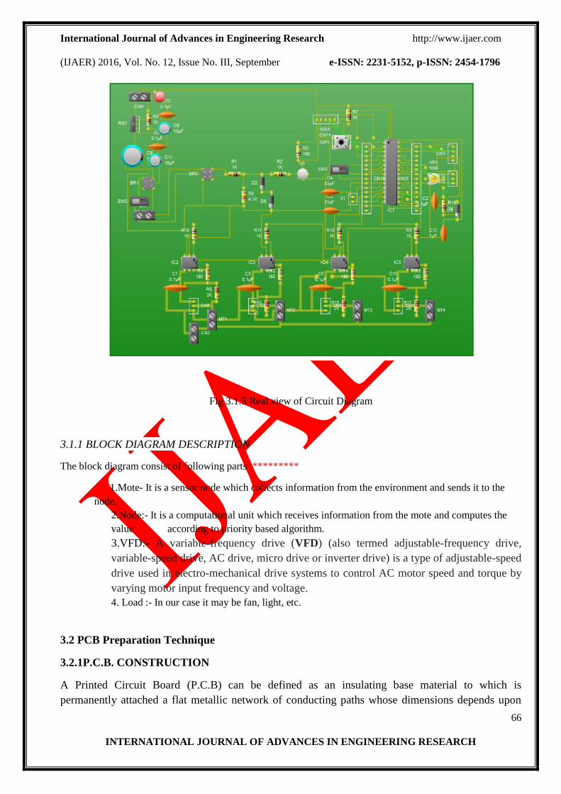
Fig 3.1.3 Real view of Circuit Diagram
3.1.1 BLOCK DIAGRAM DESCRIPTION
The block diagram consist of following parts**********
1.Mote- It is a sensor node which collects information from the environment and sends it to the
node.
2.Node:- It is a computational unit which receives information from the mote and computes the
value according to priority based algorithm.
3.VFD:- A variable-frequency drive (VFD) (also termed adjustable-frequency drive,
variable-speed drive, AC drive, micro drive or inverter drive) is a type of adjustable-speed
drive used in electro-mechanical drive systems to control AC motor speed and torque by
varying motor input frequency and voltage.
4. Load :- In our case it may be fan, light, etc.
3.2 PCB Preparation Technique
3.2.1P.C.B. CONSTRUCTION
A Printed Circuit Board (P.C.B) can be defined as an insulating base material to which is
permanently attached a flat metallic network of conducting paths whose dimensions depends upon

International Journal of Advances in Engineering Research http://www.ijaer.com
(IJAER) 2016, Vol. No. 12, Issue No. III, September e-ISSN: 2231-5152, p-ISSN: 2454-1796
67
INTERNATIONAL JOURNAL OF ADVANCES IN ENGINEERING RESEARCH
the current that can be handled by them. The P.C.B may be either single sided or double sided. The
P.C.B used for this project is single sided one.
The basic material used may be resin coated papers, fibre glass, ceramic and the flat board
configuration however is most widely used and it may be of the nature of the single "Mother Board"
into which smaller boards are plugged by the especially designed connectors which ensures adequate
and permanent low resistance coupling.
PCB designing is the most important and requires great care during work. In this case great care must
be taken while tracing the circuit or layout on the board. Because once PCB is designed, it is virtually
impossible to alter it. While designing a circuit, designer should take care to avoid crossing of
conducting paths (tracks) as possible. Crossover are unavoidable then only of the jumpers can be
used. A circuit board carrying copper on both sides can also help to solve this problem when circuit is
complicated.
The next stage lies in proportion to designing i.e. to prepare "Master Diagram ",which is commonly
made twice as the finished circuit, since this makes the working on that much easier, especially when
circuit is complicated photography eventually reduces the size of diagram to that of the circuit, before
proceeding we must know some rules regarding the designing.
1. The space between the conductors must be strictly controlled to avoid the possibility of electrical
discharge or unwanted capacitance. The amount by which the master diagram is to reduce in size is
thus a critical design feature.
2. The conductor must be wider in those parts of the circuits that are going to handle large currents
must be handle without undue temperature of conductors.
3. The minimum width of copper should not generally be less than about 1.5mm. This is related to
mechanical strength rather than the electrical properties and it also ensures that strips remains
securely bounded to the base material.
4. The points where the components holes for lead wires occurs must be sited to suit the dimensions
of the components and dimensions between lead-out wires, so that, the components can be situated
correctly on finished board. The conductor is also men large at the point of holes.
When the master diagram probable twice the size of real PCB has been evolved, the text major step
consist of etching or dissolving the unwanted metal from copper cladded board to create the circuit as
depicted by master diagram. It must be stressed that very accurate checking of master is essential at
this stage. Then, the master point is mounted on a special frame on easy facing of a larger camera and
with the aid of the very powerful illumination a master diagram is clearly photographed on a glass
sensitive plate. This is developed to give photographic negative. Next so called “step and repeat
camera." Is brought into operation. This comprises the camera body mounted so that sideways after
each exposure. In this way number of copies of the original master diagram is set out exactly to cover
standard sheet of copper clad laminate laboratory method of making PCB.

International Journal of Advances in Engineering Research http://www.ijaer.com
(IJAER) 2016, Vol. No. 12, Issue No. III, September e-ISSN: 2231-5152, p-ISSN: 2454-1796
68
INTERNATIONAL JOURNAL OF ADVANCES IN ENGINEERING RESEARCH
There are several important factors that need not be taken into account, if the finished device is to
work properly we must consider gain factor and ensure that the input and output parts are sufficiently
well isolated to avoid the possibility. We must also ensure that conductors and components carrying
high frequency current are well separated from these parts of the circuits. We are also to make sure
that all components need to return to earth are properly connected and that possibility of common
impedance arising in earth returned. Other factors that have to successfully studied include
availability of adequate return points on board and it's mounting from accessibility of switch
connections made for mechanical fixing ventilation effect of vibration.
The copper side of the board must be thoroughly cleaned before Circuit plan is transferred to it. This
is very important because even slightest trace of graze (from figure of instance) will impure the
etching process and When the circuit plan has been neatly transferred to copper in this manner the
board is held under, running tap and the allowed to dry before resist is applied.
Now, once cleaning is done plan has to transfer on copper surface of PCB material. A convenient
way to do this is simply put a carbon paper between a copper surface of the board and working plan
and carefully trace the lines of original plan with a ball pen.
Resist is nothing more than a substrate that is unaffected by presence etching chemicals. It is usually
coloured so that, it can be easily seen the copper surface. When plan is clearly worked on clean
copper then that are to be left in fact as the copper conductors must be covered when resists the
leaguer type of paints possess good resist properties but disadvantages of relatively long time taken
for drying. It is essential to resist through hardening before etching is started. Nail polished are better
as they quickly and are less difficult to remove. Now-a-days etching taps along with IC pads are
commonly used. To this, chances of short circulating due to paints are completely the avoid etching
tapes and pads are available in different sizes.
When a result has been thoroughly hardened any errors that have been made can usually be corrected
by gently scratching away with knife. To ensure clear out lines round edges of copper conductors on
board the resist must be applied with steady band. Next comes etching of unwanted copper and
whether a small single is all that is required as quantity of board to be produce certain precautions
must be taken before operation is commenced the most etch ant I ferric chloride and to this is added
small quantity of HCL to accelerate, But not critical as lab construction is concerned. Mixing 10
grams of ferric chloride and 25 grams of HCL with 15 grams of water can produce a good etchant.
Small plastic bath is ideal for storing the etchant process. The Depth of liquid must be sufficient to
completely cover laminate, the laminated board carrying the resist pattern circuit is then dropped into
etchant bath and the gentle agitation takes 5 to 20 minutes to complete depending on the strength of
the etchant temperature and thickness of copper foil.
When all unwanted copper is dissolved from areas between conductors, board should be taken from
an etchant and washed in water. The resist must be removed using proper solvent. After this the
copper surface must be polished with any kind of cleaner. It should be seen that there is no slight
incomplete etching between the conducting paths of the PCB. The PCB's are coated coating material
for protection in lab coating material itself is a solder. This process is called Tinning. This process of

International Journal of Advances in Engineering Research http://www.ijaer.com
(IJAER) 2016, Vol. No. 12, Issue No. III, September e-ISSN: 2231-5152, p-ISSN: 2454-1796
69
INTERNATIONAL JOURNAL OF ADVANCES IN ENGINEERING RESEARCH
coating involves tracks with soldier. Advantage of tinning the effect of environment of conductors,
then PCB is drilled i.e. holes for filling and mounting the components on PCB are drilled with
suitable drill bit.
After the holes are drilled, the components have to be assembled on PCB before assembling the
components it is necessary to clean soldering iron in order to get easy and accurate soldering.
Removing impurity particles that are gathered on iron bit due to repetitive use cleans soldering iron.
PCB Layout
Fig. 3.x PCB Layout of Circuit
3.3 Components List
Component Value Quantity Rate Total
Bridge Converter 2
Resistor
180 Ω, 5W 4 6 24
2k Ω, 5W 4 6 24

International Journal of Advances in Engineering Research http://www.ijaer.com
(IJAER) 2016, Vol. No. 12, Issue No. III, September e-ISSN: 2231-5152, p-ISSN: 2454-1796
70
INTERNATIONAL JOURNAL OF ADVANCES IN ENGINEERING RESEARCH
1 KΩ 9 1 9
4.7KΩ 1 1 1
10 KΩ 1 1 1
Capacitor
1 µF 4 1 4
1 µF, AC 4 5 20
10 µF 2 3 6
1000 µF 1 10 10
33 pF 2 1 2
LED Green 1 1 1
Diode 1N4007 2 1 2
Oscillator 16 MHz 1 10 10
Voltage Regulator IC 7805 1 24 24
Microcontroller Atmel 328 1 180 180
Xbee S2 3 1200 3600
Optocoupler MOC 3021 4
ACS 712 5A 1 300 300
16 X 2 LCD JHD 162A 1 180 180
Variable Resistor 10KΩ 1 5 5

International Journal of Advances in Engineering Research http://www.ijaer.com
(IJAER) 2016, Vol. No. 12, Issue No. III, September e-ISSN: 2231-5152, p-ISSN: 2454-1796
71
INTERNATIONAL JOURNAL OF ADVANCES IN ENGINEERING RESEARCH
Zener Diode BTA 16 1
Transistors 2N2222 1 3 3
PIR Sensor 1 180 180
LDR 1 10 10
LM 35 1 50 50
Channel Input 7 3 21
Switches
Push to On 1 2
2
Toggle 2 5 10
Table 3.1 Component List
3.4 Software Implementation
We use different software in our project which as follows:
PCB Wizard:
PCB Wizard is used for designing of circuit and PBC Layout. It provides a comprehensive range of
tools covering all the traditional steps in PCB production, including schematic drawing, schematic
capture, component placement, automatic routing, Bill of Materials reporting and file generation for
manufacturing.
XCTU:
XCTU is a free multi-platform application designed to enable developers to interact with Digi RF
modules through a simple-to-use graphical interface. It includes new tools that make it easy to set-up,
configure and test XBee® RF modules.
XCTU includes all of the tools a developer needs to quickly get up and running with XBee. Unique
features like graphical network view, which graphically represents the XBee network along with the
signal strength of each connection, and the XBee API frame builder, which intuitively helps to build

International Journal of Advances in Engineering Research http://www.ijaer.com
(IJAER) 2016, Vol. No. 12, Issue No. III, September e-ISSN: 2231-5152, p-ISSN: 2454-1796
72
INTERNATIONAL JOURNAL OF ADVANCES IN ENGINEERING RESEARCH
and interpret API frames for XBees being used in API mode, combine to make development on the
XBee platform easier than ever.
Other highlights of XCTU include the following features:
You can manage and configure multiple RF devices, even remotely (over-the-air)
connected devices.
The firmware update process seamlessly restores your module settings, automatically
handling mode and baud rate changes.
Two specific API and AT consoles, have been designed from scratch to communicate with
your radio devices.
You can now save your console sessions and load them in a different PC running XCTU.
XCTU includes a set of embedded tools that can be executed without having any RF module
connected:
o Frames generator: Easily generate any kind of API frame to save its value.
o Frames interpreter: Decode an API frame and see its specific frame values.
o Recovery: Recover radio modules which have damaged firmware or are in
programming mode.
o Load console session: Load a console session saved in any PC running XCTU.
o Range test: Perform a range test between 2 radio modules of the same network.
o Firmware explorer: Navigate through XCTU's firmware library.
Arduino Uno:
The Arduino integrated development environment (IDE) is a cross-platform application written
in Java, and derives from the IDE for the Processing programming language and the Wiring projects.
It is designed to introduce programming to artists and other newcomers unfamiliar with software
development. It includes a code editor with features such as syntax highlighting, brace matching, and
automatic indentation, and is also capable of compiling and uploading programs to the board with a
single click. A program or code written for Arduino is called a "sketch".
Algorithm for the circuit
1] Start.
In this step after switching on the power supply the circuit gets on and LED glows showing that the
circuit is properly working.
2] Formation of Wireless network using Xbees.
We have used Xbees for wireless communication and to get the information of sensor wirelessly.
3]Connecting different sensor with Xbees and wireless network
We are using different sensor which are connected with Xbees and the information of sensor are send
to Micro-controller wireless by the use network made using Xbees.

International Journal of Advances in Engineering Research http://www.ijaer.com
(IJAER) 2016, Vol. No. 12, Issue No. III, September e-ISSN: 2231-5152, p-ISSN: 2454-1796
73
INTERNATIONAL JOURNAL OF ADVANCES IN ENGINEERING RESEARCH
4] Priority selection of loads.
The end user can set priority to the load according to demand of the person.
5]Power Measurement
We have developed a power measurement circuit, to know the amount of power being consumed at
the instance. The Micro-controller will be able to know the amount of power being consumed at an
instance.
6] PWM
A Predefined amount of power is set in the micro-controller. If the power Measured from power
measurement circuit exceeds the predefined amount of power, then PWM will be done. The load with
lowest priority will be modulated first and so on.
5] Automation
Depending on the information of sensor, coming from xbees wireless, Micro-controller will perform
Automation i.e automatic turning on and off of loads.
3.5 Flowchart
We have replace with our flowchart , this is not ours.

International Journal of Advances in Engineering Research http://www.ijaer.com
(IJAER) 2016, Vol. No. 12, Issue No. III, September e-ISSN: 2231-5152, p-ISSN: 2454-1796
74
INTERNATIONAL JOURNAL OF ADVANCES IN ENGINEERING RESEARCH
Fig. 3.10 Flowchart of Operation
The flowchart shown in fig. describes the complete functioning of the project Gesture controlled
home appliances. This prototype of the Gesture controlled home appliances was efficiently designed.
The LED of circuit gets on after switching on the power supply. This prototype has facilities to be
integrated with a display board thus making it truly mobile. The sensor detects various gestures,
controls switching of the relays and notifies everyone by displaying it on LCD module. The gesture is
Include header files
Define port , Define lcd ,
Initialize sensor adc , serial port
Display welcome message
Read value from sensor
Send it to serial port
No If sensor
value>set
value
Take defined action
Led 1 glow
Yes
Define byte/word /bit
Define variables
Start

International Journal of Advances in Engineering Research http://www.ijaer.com
(IJAER) 2016, Vol. No. 12, Issue No. III, September e-ISSN: 2231-5152, p-ISSN: 2454-1796
75
INTERNATIONAL JOURNAL OF ADVANCES IN ENGINEERING RESEARCH
detected from the Accelerometer each time it is changed, and it again change the device status, thus
change in the message on the LCD module. In this case, it can solve the problem of instant switching
of appliances in the home.

International Journal of Advances in Engineering Research http://www.ijaer.com
(IJAER) 2016, Vol. No. 12, Issue No. III, September e-ISSN: 2231-5152, p-ISSN: 2454-1796
76
INTERNATIONAL JOURNAL OF ADVANCES IN ENGINEERING RESEARCH
Chapter 4
Results And Discussions
4.1 Hardware Result
Fig 4.1 Output of Zero CROSSING Detector and PWM.
The sensor value is acquired by the xbee and it is transmitted to another xbee depending on that the
power is modulated. The keypad is used to set the priorities to the load. Depending on the priorities
the power on the load will be modulated and the amount of power that is measured using ACS712 is
being displayed on the LCD. The above images shows that the we have successfully got Zero
Crossing detector and PWM.
The output can seen in DSO.

International Journal of Advances in Engineering Research http://www.ijaer.com
(IJAER) 2016, Vol. No. 12, Issue No. III, September e-ISSN: 2231-5152, p-ISSN: 2454-1796
77
INTERNATIONAL JOURNAL OF ADVANCES IN ENGINEERING RESEARCH
Fig 4.2 Output of PWM.
The above image shows that the circuit is working properly and the bulb is on and PWM is done by
small amount.
Fig. 4.3 Output of PWM with Low Intensity
The above shows that circuit is working properly and we are getting proper output and the image
shows that we have done Modulation and the intensity of bulb is reduced.
4.2 Software Result
The input from Zero crossing detector goes as interrupt to the microcontroller, as soon as the
microcontroller receives it reads the value that is being received by the xbee and accordingly it sends
the pulse to optocoupler. According to the input at keypad matrix the priorites of the load is set i.e.
some percentage of power modulation takes place.

International Journal of Advances in Engineering Research http://www.ijaer.com
(IJAER) 2016, Vol. No. 12, Issue No. III, September e-ISSN: 2231-5152, p-ISSN: 2454-1796
78
INTERNATIONAL JOURNAL OF ADVANCES IN ENGINEERING RESEARCH
Chapter 5
Conclusion
5.1 Summary
The project Development of “Distributed power system using ZigBee Technology ” is an effective
system for controlling home and office appliances. The system is small, simple and good for
appliances control.
The System “Distributed power system using ZigBee Technology ” will help constrain power
consumption without human intervention. It will help to restrain electricity bill (threshold can be
decided by the user).Using this system energy consumption data can be monitored and audited for
devising future power consumption strategies. System can be controlled from a remote location due
to internet connectivity.
5.2 Future Scope
This idea can be extended to loads connected in multiple rooms even up to the entire building. This
system can be made applicable in Smart Cities where systems are controlled from a remote location.
This system will help us to maintain the database of energy consumption in different units. This will
be major step in automation and will have tremendous future scope of development and applications.
AUTHORS
First Author –Tejas Mahale , B.E., Electronics & Telecommunication Department,
P.V.P.P.C.O.E,Mumbai,Maharashtra, India.
Second Author –Roshan Khandare, B.E., Electronics & Telecommunication, P.V.P.P.C.O.E,
Mumbai, Maharashtra, India.
Third Author –Vinu Vinayan, B.E., Electronics & Telecommunication
P.V.P.P.C.O.E,Mumbai,Maharashtra, India.


![catalog 05 - Siam2Web.comfile.siam2web.com/sekpsb/files[document]/catalog/2014417_69573.pdf · pir-ooi 14x62 pir-tt-00002 202 10x74 pir-tt-00003 14x62 1 pir-rr-00001 2. 3.](https://static.fdocuments.in/doc/165x107/5c1c806e09d3f23c268c0e19/catalog-05-documentcatalog201441769573pdf-pir-ooi-14x62-pir-tt-00002.jpg)