Direct wafer bonding for MEMS and microelectronics - VTT
106
ESPOO 2006 VTT PUBLICATIONS 609 Tommi Suni Direct wafer bonding for MEMS and microelectronics
Transcript of Direct wafer bonding for MEMS and microelectronics - VTT
VTT PU
BLICATIO
NS 609
Direct w
afer bonding for MEM
S and microelectronics
Tomm
i Suni
Tätä julkaisua myy Denna publikation säljs av This publication is available from
VTT VTT VTTPL 1000 PB 1000 P.O. Box 1000
02044 VTT 02044 VTT FI02044 VTT, FinlandPuh. 020 722 4404 Tel. 020 722 4404 Phone internat. +358 20 722 4404Faksi 020 722 4374 Fax 020 722 4374 Fax +358 20 722 4374
ISBN 951– 38– 6851– 6 (soft back ed.) ISBN 951– 38– 6852– 4 (URL: http://www.vtt.fi/inf/pdf/)ISSN 1235– 0621 (soft back ed.) ISSN 1455– 0849 (URL: http://www.vtt.fi/inf/pdf/)
ESPOO 2006 VTT PUBLICATIONS 609
Tommi Suni
Direct wafer bondingfor MEMS and microelectronics
Direct wafer bonding is a method for fabricating advanced substrates formicroelectromechanical systems (MEMS) and integrated circuits (IC). Themost typical example of such an advanced substrate is the silicononinsulator (SOI) wafer. Direct wafer bonding can also be used in thefabrication of more complex structures than SOI. The wafers to be bondedcan be of different materials, can contain patterns, and may have multiplelayers or readymade devices.
This thesis reports on studies of direct wafer bonding and its use invarious applications. The main focus of the thesis is on the plasmaactivationbased low temperature bonding process, and on the control ofbond strength by surface preparation.
A novel method for bond strength measurement is introduced. Thismethod, based on buried oxide etching, is presented and compared withother methods used in evaluating bond quality.
This thesis also contains results on research of different applicationsrequiring direct wafer bonding. Heterogeneous integration, preprocessedSOI fabrication, and wafer scale packaging are the main application topics.


VTT PUBLICATIONS 609
Direct wafer bonding for MEMS and microelectronics
Tommi Suni
Dissertation for the degree of Doctor of Science in Technology to be presented with due permission of the Department of Materials Science and Engineering, for public examination and debate in Auditorium V1 at Helsinki University of Technology
(Espoo, Finland) on 18th of August, 2006, at 12 noon.

ISBN 951ñ38ñ6851ñ6 (soft back ed.) ISSN 1235ñ0621 (soft back ed.)
ISBN 951ñ38ñ6852ñ4 (URL: http://www.vtt.fi/publications/index.jsp) ISSN 1455ñ0849 (URL: http://www.vtt.fi/publications/index.jsp)
Copyright © VTT Technical Research Centre of Finland 2006
JULKAISIJA ñ UTGIVARE ñ PUBLISHER
VTT, Vuorimiehentie 3, PL 1000, 02044 VTT puh. vaihde 020 722 111, faksi 020 722 4374
VTT, Bergsmansvägen 3, PB 1000, 02044 VTT tel. växel 020 722 111, fax 020 722 4374
VTT Technical Research Centre of Finland, Vuorimiehentie 3, P.O.Box 1000, FIñ02044 VTT, Finland phone internat. +358 20 722 111, fax + 358 20 722 4374
VTT, Tietotie 3, PL 1000, 02044 VTT puh. vaihde 020 722 111, faksi 020 722 7012
VTT, Tietotie 3, PB 1000, 02044 VTT tel. växel 020 722 111, fax 020 722 7012
VTT Technical Research Centre of Finland, Tietotie 3, P.O. Box 1000, FI-02044 VTT, Finland phone internat. +358 20 722 111, fax +358 20 722 7012
Technical editing Leena Ukskoski Otamedia Oy, Espoo 2006

3
Suni, Tommi. Direct wafer bonding for MEMS and microelectronics [Puolijohdekiekkojen suoraliittäminen mikroelektroniikan ja mikromekaniikan sovellutuksissa]. Espoo 2006. VTT Publications 609. 89 p. + app. 34 p.
Keywords direct wafer bonding, MEMS, microelectronics, microelectromechanical systems,SOI, silicon-on-insulator, integrated circuits, bond strength measurement,heterogeneous integration, pre-processed SOI fabrication, wafer-scale packaging, plasma activation
Abstract Direct wafer bonding is a method for fabricating advanced substrates for microelectromechanical systems (MEMS) and integrated circuits (IC). The most typical example of such an advanced substrate is the silicon-on-insulator (SOI) wafer. SOI wafers offer many advantages over conventional silicon wafers. In IC technology, the switching speed of circuits fabricated on SOI is increased by 20-50% compared to circuits fabricated on a bulk Si wafer. The required operation voltage is lower in ICs on SOI than in ICs on a bulk silicon wafer, which decreases power consumption and chip heating. In the MEMS industry, the buried oxide layer works as a good sacrificial layer during release etching of diaphragms, beams etc. and offers an excellent etch stop layer for silicon etching. Direct wafer bonding can also be used in the fabrication of more complex structures than SOI. The wafers to be bonded can be of different materials, can contain patterns, and may have multiple layers or ready-made devices.
This thesis reports on studies of direct wafer bonding and its use in various applications. Different bonding processes used in microelectronics are briefly described. The main focus of this thesis is on the plasma activation-based low temperature bonding process, and on the control of bond strength by surface preparation.
A novel method for bond strength measurement is introduced. This method, based on buried oxide etching, is presented and compared with other methods used in evaluating bond quality.
This thesis also contains results on research of different applications requiring direct wafer bonding. Heterogeneous integration, pre-processed SOI fabrication, and wafer scale packaging are the main application topics.

4
Suni, Tommi. Direct wafer bonding for MEMS and microelectronics [Puolijohdekiekkojen suoraliittäminen mikroelektroniikan ja mikromekaniikan sovellutuksissa]. Espoo 2006. VTT Publications 609. 89 s. + liitt. 34 s.
Avainsanat direct wafer bonding, MEMS, microelectronics, microelectromechanical systems,SOI, silicon-on-insulator, integrated circuits, bond strength measurement,heterogeneous integration, pre-processed SOI fabrication, wafer-scale packaging, plasma activation
Tiivistelmä Puolijohdekiekkojen suoraliittäminen on menetelmä valmistaa kehittyneitä alustoja mikroelektromekaanisille systeemeille (MEMS) ja integroiduille piireille. Yleisin tämänlainen kehittyneempi alusta on SOI-kiekko, jossa kantajakiekon ja varsinaisen komponenttipiikerroksen välissä on eristävä oksidikerros. Verrattuna tavallisiin piikiekkoihin SOI-kiekot tarjoavat useita parannuksia. Integroitujen piirien tapauksessa kytkentänopeus on SOI:lla 20ñ50 % nopeampi, käyttöjännite matalampi ja energian kulutus pienempi. MEMS-teknologiassa haudattu oksidi toimii uhrautuvana kerroksena kalvojen ja palkkien vapautusetsauksessa ja myös pysäytyskerroksena piin syövyttämisessä. Suoraliittämistä voidaan käyttää myös monimutkaisempien rakenteiden kuin SOI-kiekkojen valmistamiseen. Liitettävät kiekot voivat olla eri materiaaleista, kuvioituja tai sisältää valmiita komponentteja.
Tässä väitöskirjassa keskitytään pääasiassa korkean ja matalan lämpötilan suoraliittämiseen sekä liitoslujuuden kontrollointiin pintoja karhentamalla. Kir-jassa esitellään lyhyesti myös muut kiekkoliitostekniikat.
Väitöskirjassa raportoidaan myös uusi menetelmä mitata liitoslujuus kahden kiekon välillä. Menetelmä perustuu haudatun oksidin märkäsyövyttämiseen ja sitä verrataan myös muihin raportoituihin liitoslujuuden mittausmenetelmiin.
Tämä väitöskirja sisältää myös tuloksia suoraliittämisen käyttämisestä muutamiin erilaisiin sovellutuksiin, kuten kiekkotason paketointiin, heterogee-niseen integrointiin ja esiprosessoitujen SOI-kiekkojen valmistukseen.

5
Preface This work has been carried out at VTT Microelectronics. I would like to thank first my co-workers at VTT for their help and support. Especially I would like to thank Kimmo Henttinen and Hannu Luoto for their assistance in the experimental work as well as in writing the articles. I would also like to thank my advisor Dr. Jari Mäkinen and my supervisor Prof. Ari Lehto for their guidance during final writing process. Thanks also to Dr. Jukka Lahtinen and Dr. Anke Sanz-Velasco for pre-examining the thesis and for Prof. Nathan Cheung for agreeing to be my opponent in the public defence of the thesis.
A lot of people have also been helping me and pushing me forward during all these years of studying making the writing of this thesis possible, so special thanks to: Äiti, T. Fält, E. Valovirta, J. Niemistö, T. Kaskiala, R. Jansson, K. Kaskiala, V. Sompa, J. Ylikerälä, J. Repo, A. Hirvonen, I. Suni, M. Kulawski, S. S. Lau, T. Penttinen, T. Tuominen, O. Alanen, A. Laukkanen, A. Saaristo, T. Tulkki, T. Karila, S. Mustala, S. Nurmi and also to my father and to my brothers.
Espoo, July 2006
Tommi Suni

6
Contents
Abstract ................................................................................................................. 3
Tiivistelmä ............................................................................................................ 4
Preface .................................................................................................................. 5
List of abbreviations and terms............................................................................. 8
List of publications ............................................................................................. 10
1. Introduction................................................................................................... 13 1.1 Objectives of this thesis....................................................................... 13 1.2 Summary of appended papers.............................................................. 14
2. Bonding......................................................................................................... 15 2.1 Direct bonding (high temperature) ...................................................... 15
2.1.1 Hydrophilic high temperature bonding of silicon ................... 16 2.1.2 Hydrophobic high temperature bonding of silicon.................. 18
2.2 Low-temperature direct bonding ......................................................... 20 2.2.1 Plasma activation based low-temperature bonding ................. 21 2.2.2 Ultra-high vacuum low-temperature hydrophobic bonding.... 22
2.3 Bonding of chemical vapour deposited (CVD) oxides........................ 23 2.4 Bonding of chemical vapour deposited silicon.................................... 28 2.5 Anodic bonding ................................................................................... 29 2.6 Adhesive and polymer bonding........................................................... 30 2.7 Metallic bonding.................................................................................. 30 2.8 Glass frit bonding ................................................................................ 31
3. Methods for evaluating bonding quality ....................................................... 32 3.1 Methods to estimate the bondability of wafers.................................... 32
3.1.1 Atomic force microscopy (AFM)............................................ 32 3.1.2 Surface profilometry ............................................................... 33 3.1.3 Particle detection..................................................................... 34
3.2 Bond strength measurements............................................................... 34 3.2.1 The crack opening method ...................................................... 35 3.2.2 Pulling test (or tensile test)...................................................... 35

7
3.2.3 Blister test ............................................................................... 36 3.2.4 HF etching test ........................................................................ 37 3.2.5 Chevron test ............................................................................ 40
3.3 Void detection ..................................................................................... 42 3.3.1 Optical inspection.................................................................... 42 3.3.2 Scanning acoustic microscopy (SAM).................................... 43
4. Applications of Wafer Bonding.................................................................... 46 4.1 Silicon-on-Insulator (SOI)................................................................... 46
4.1.1 Thin film SOI .......................................................................... 47 4.1.2 Thick film SOI ........................................................................ 50 4.1.3 Intermediate SOI (device layer thickness 2ñ5 µm)................. 50 4.1.4 Strained silicon-on-insulator (sSOI)........................................ 50 4.1.5 Cavity SOI............................................................................... 54 4.1.6 Multi-layer SOI ....................................................................... 59
4.2 Heterogeneous integration................................................................... 62 4.2.1 Compliant substrates ............................................................... 63
4.3 Wafer scale packaging......................................................................... 65 4.3.1 Planarization and polishing ..................................................... 66 4.3.2 Direct bonding of MEMS wafer.............................................. 70 4.3.3 Fabrication of electrical contacts............................................. 71
5. Temporary wafer bonding ............................................................................ 73 5.1 Temporary wafer bonding using impurity outgassing of CVD oxides 75 5.2 Temporary wafer bonding using surface roughening.......................... 76
6. Summary....................................................................................................... 80
References........................................................................................................... 82
Appendices Publications AñF

8
List of abbreviations and terms AFM Atomic force microscope
APCVD Atmospheric pressure chemical vapour deposition
BOX Buried oxide
Cap wafer Also known as device wafer. Top wafer in SOI wafer, thinned to desired SOI thickness
CMP Chemical-mechanical polishing/planarization
CTE Coefficient of thermal expansion
Device wafer See cap wafer
DIW Deionized water
DSP Double side polished (wafer)
FBAR Film bulk acoustic resonator
GaAs Gallium arsenide
Handle wafer Bottom wafer in SOI, the wafer that is usually not thinned
IC Integrated circuit
InP Indium phosphite
IR Infrared
LPCVD Low pressure chemical vapour deposition
MEMS Microelectromechanical system
NIR Near infrared
OH Hydroxyl
9
PECVD Plasma enhanced chemical vapour deposition
RMS Root mean square
SAM Scanning acoustic microscope
SC-1 Standard cleaning 1, also known as RCA-1. Typical cleaning bath for silicon wafers which removes particles and makes the surface hydrophilic.
SEM Scanning electron microscope
SIMOX Separation by oxygen implantation, one way to fabricate SOI
Si-OH Silanol
Smart Cutô Hydrogen implantation based method to make thin silicon layers
SOG Silicon-on-glass
SOI Silicon-on-insulator
SOQ Silicon-on-quartz
SOS Silicon-on-sapphire
sSOI Strained silicon-on-insulator
SSP Single side polished (wafer)
TTV Total thickness variation
UHV Ultra-high vacuum
Void Discontinuation on the bonded interface
10
List of publications This work is based on the following papers (Publications A�F), referred to in the text by the relevant letter in bold:
List of appended publications:
A. T. Suni, K. Henttinen, I. Suni, and J. Mäkinen. Effects of plasma activation on hydrophilic bonding of Si and SiO2. Journal of the Electrochemical Society, Vol. 149, No. 6, (2002), pp. G348ñ351.
B. T. Suni, K. Henttinen, A. Lipsanen, J. Dekker, H. Luoto, and M. Kulawski. Wafer scale packaging of MEMS by using plasma-activated wafer bonding. Journal of the Electrochemical Society, Vol. 153, No. 1, (2006), pp. G78ñ82.
C. T. Suni, K. Henttinen, J. Dekker, H. Luoto, M. Kulawski, J. Mäkinen, and R. Mutikainen. SOI wafers with buried cavities. Journal of the Electrochemical Society, Vol. 153, No. 4, (2006), pp. G299ñG303.
D. T. Suni, J. Kiihamäki, K. Henttinen, I. Suni, and J. Mäkinen. Characterization of bonded interface by HF etching method. In Semiconductor Wafer Bonding: Science, Technology and Applications VII, edited by C. Hunt, H. Baumgart, S. Bengtsson, T. Abe, Electrochemical Society, pp. 70ñ75, 2003.
E. K. Henttinen, T. Suni, A. Nurmela, M. Kulawski, and I. Suni. Mechanical delamination for the materials integration. In Semiconductor Wafer Bonding: Science, Technology and Applications VII, edited by C. Hunt, H. Baumgart, S. Bengtsson, T. Abe, Electrochemical Society, pp. 359ñ367, 2003.
F. K. Henttinen, T. Suni, A. Nurmela, H. Luoto, I. Suni, V.-M. Airaksinen, S. Karirinne, M. Cai, and S. S. Lau. Transfer of thin Si layers by cold and thermal ion cutting. Journal of Material Science: Materials in Electronics, 14, (2003), pp. 299ñ303.

11
Authorís contribution
In Publication A, the author planned the experimental work together with co-authors, performed the experimental work and wrote the manuscript with the help of the co-authors.
In Publication B, the author planned and performed the experimental work together with the co-authors and wrote the manuscript with their help.
In Publication C, the author planned and performed the experimental work together with the co-authors and wrote the manuscript with K. Henttinen.
In Publication D, the author planned and performed the experimental work and wrote the manuscript, taking into account comments by the co-authors.
In Publication E, the author planned the experimental work together with K. Henttinen and performed the experimental work together with other authors. The manuscript was written with K. Henttinen, taking into account comments by the other co-authors.
Publication F is a joint paper together with researchers from VTT, Okmetic Oyj, Tampere University of Technology and the University of California, San Diego. The main experimental work was planned and performed at VTT by the author and K. Henttinen. The manuscript was written by K. Henttinen and the author with the help of the other co-authors.


13
1. Introduction Direct wafer bonding means joining two surfaces without intermediate adhesives or external force. If the surfaces are flat and clean, wafers bond together when brought into contact. The initial bond strength is usually weak. Therefore, a subsequent annealing step is generally carried out to strengthen the bond.
Direct bonding was first reported by Sir Isaac Newton in the 17th century. He observed a black spot surrounded by ìNewtonís ringsî when a flat and a convex optical surface were brought into contact. [1]
Currently direct wafer bonding has many applications in the microelectronics industry. It is used to fabricate substrates for modern integrated circuits (SOI, SOG, SOS, sSOI), to stack many processed layers (3D-integration) and as a method to encapsulate MEMS devices. These different applications require usually more than just a typical silicon wafer bonding process (wafer contacting and annealing at 1100°C). Bonding of processed wafers or wafers with a large difference in thermal expansion coefficients requires a low-temperature bonding process. Surface preparation may also be required before wafer contacting, the most typical process steps being plasma activation, chemical cleaning and chemical-mechanical polishing.
1.1 Objectives of this thesis
The main objectives of this thesis were first to study low temperature direct bonding, then to develop bonding processes suitable for various applications, such as fabrication of silicon-on-glass (SOG), silicon-on-sapphire (SOS), and silicon-on-insulator substrates with buried cavities, as well as for wafer scale packaging of MEMS components. This study also introduces a bond strength measuring technique based on the etching of buried oxide with hydrofluoric acid. This method is suitable for evaluating the bond strength easily from ready-made SOI, diced samples and from small bonded areas, which are difficult or impossible to measure with the crack opening method. This thesis focuses on bonding of silicon, but the same requirements apply to bonding of other semiconductor materials as well: surfaces have to be flat, smooth and clean.

14
1.2 Summary of appended papers
This thesis includes six publications on the topic of wafer bonding.
Publication A reports on the influence of plasma activation on wafer bonding and lists measured bond strengths for different bonding process combinations.
Publication B describes two different methods for encapsulating MEMS devices at wafer level utilizing plasma activated wafer bonding.
Publication C reports some design rules for fabrication of pre-processed SOI wafers for MEMS applications.
Publication D describes a method for measuring the bond strength of samples where the crack opening method cannot be used. Characterization of the bond strength by measurement of the buried oxide etch rate is, for example, applicable to small chips, silicon-to-glass and silicon-to-quartz bondings, which are difficult or impossible to measure with conventional methods.
Publication E presents a method for controlling the bond strength between two wafers. Good bond strength control creates possibilities to fabricate substrates that would be difficult or impossible to achieve with conventional methods (e.g. single crystalline silicon-on-sapphire)
Publication F describes a cold-cut process for fabrication of thin film SOI and SOG wafers. It also describes the influence of boron doping and crystal orientation on surface energy of the implanted layer after various annealing temperatures, setting the requirements for the bonding process.

15
2. Bonding Bonding in general means the joining of two pieces of the same or a different material together. Bonding can be divided into three categories: bonding with a conducting interlayer, with an insulating interlayer, or without an intermediate layer. All of these categories are used extensively in the microelectronics industry. The bonding methods and their advantages and drawbacks are listed in Table 1. In this thesis, the focus is on hydrophilic direct bonding and low temperature direct bonding. Direct bonding means that there is no intermediate layer between the wafers, and the wafer surfaces bond spontaneously.
Table 1. Bonding techniques used in microelectronics.
2.1 Direct bonding (high temperature)
Direct bonding or fusion bonding generally means any joining of two materials without an intermediate layer or external force. In principle, most materials bond

16
together if their surfaces are flat, smooth and clean. The principle of this method is simple: two flat, clean and smooth wafer surfaces are brought into contact and form a weak bonding based on physical forces. The physical forces can be van der Waals forces, capillary forces or electrostatic forces [2]. The wafer pair is then annealed at high temperature (in the case of hydrophilic Si at >1000°C) and the physical forces are converted to chemical bonds. A typical process flow for wafer bonding is presented in Figure 1. In the case of silicon, high temperature bonding falls into two categories: hydrophilic bonding, in which the bonded surfaces are silicon dioxide, and hydrophobic bonding, in which the surfaces are silicon.
Figure 1. a) Surface preparations (e.g. cleaning, polishing, surface activation) b) Wafer contacting c) Annealing.
2.1.1 Hydrophilic high temperature bonding of silicon
Hydrophilic high temperature bonding is used commercially, for example, in SOI wafer manufacturing. The typical annealing temperature is ~1100°C. In hydrophilic bonding of silicon, the silicon wafer surface is covered with an oxide layer. The oxide can be a thin native oxide, thermally grown oxide or deposited oxide. The surface contains Si-O-Si and Si-OH bonds. It is the amount of Si-OH (silanol) groups on the surface that determines the hydrophilicity of the surface

17
due to polarization of the hydroxyl (OH) groups. The hydrophilicity of the surface can be enhanced with various methods, of which most popular is warm SC-1 (1:1:5 NH3:H2O2:H2O solution).
The reaction between two hydrophilic silicon surfaces during bonding is depicted in Figure 2. At the initial state after establishing contact between the wafers, water molecules form a ìbridgeî between the surfaces (Figure 2a). During annealing these water molecules diffuse out from the interface, dissolve into the surrounding material or react with surfaces increasing the number of silanol groups on the surface. Once these water molecules are removed, a bond is formed between silanol groups (Figure 2b). During further annealing, opposing silanol groups react according to reaction 1.
Si-OH + Si-OH = Si-O-Si + H2O (1)
During this reaction between silanol groups, more water molecules are released and Si-O-Si bonding is formed (Figure 2c).
Figure 2. a) Bonding via intermediate water molecules, b) Bonding between two OH groups by van der Waals forces, and c) Formation of Si-O-Si bonds [2].

18
The water molecules diffuse into the silicon dioxide on the surfaces. If the water reaches the silicon, it reacts with it to form silicon dioxide and hydrogen.
Si + 2 H2O = SiO2 + 2 H2 (2)
The remaining hydrogen does not react with silicon and may cause problems in the form of trapped gas, which is detectable with an IR camera or scanning acoustic microscopy (SAM) as voids (Figure 3). However, hydrogen has a high solubility into SiO2 and by having an oxide layer of thickness > 50 nm on at least one wafer surface, hydrogen-induced voids can be avoided. The required amount of oxide on the surfaces for completely dissolving the hydrogen depends on the amount of water present at the interface. It can be enhanced by changing the hydrophilicity of the surfaces with different surface preparations and by using different bonding atmospheres.
Figure 3. Hydrogen-induced voids in a bonded wafer pair. Both wafer surfaces had only ~2 nm thick native oxide, which cannot accommodate all of the hydrogen formed during the process.
2.1.2 Hydrophobic high temperature bonding of silicon
Hydrophobic bonding is a method for replacing epitaxial growth in some applications during fabrication of Si wafers with variously doped Si layers. For example, p-n junctions can be fabricated by bonding p-doped Si to an n-doped Si

19
wafer. It is also used to fabricate compliant substrates by twist bonding. In hydrophobic Si bonding, silicon is directly joined to another silicon wafer without an intermediate oxide.
In hydrophobic bonding, the wafers to be bonded have a bare silicon surface, which is either hydrogen and fluorine terminated or in some cases has dangling bonds on the surface. A hydrogen and fluorine terminated surface results from hydrofluoric acid etching, which is a standard process for removing silicon dioxide. The hydrophobic surface is quickly contaminated with hydrocarbons, therefore the wafers should be quickly contacted or stored in a vacuum after removal of the silicon dioxide layer [3].
The bonding process is illustrated in Figure 4. At first the HF molecules form a bridge between two silicon surfaces. At temperatures from 150°C-300°C, the HF molecules are rearranged and additional bonds are formed. During annealing at 300°Cñ700°C, hydrogen desorbs from the surfaces and Si-Si bonds are formed according to reaction 3 [2].
Si-H + Si-H = Si-Si +H2 (3)
During annealing at >700°C, surface diffusion of silicon takes place and closes the microgaps between the surfaces [2]. The problem with the bonding process is again the presence of hydrogen at the bonded interface, which may cause voids.

20
Figure 4. a) Bonding via HF molecules, b) Bonding via H & F atoms with van der Waals forces, c) Si-Si bonding formed after high-temperature annealing [2].
2.2 Low-temperature direct bonding
A low-temperature bonding process may be needed if the wafers are pre-processed, contain temperature-sensitive materials or components, or have different thermal expansion coefficients. The most common methods used for low-temperature hydrophilic direct wafer bonding are based on plasma activation [Publication A, 4, 5, 6, 7]. In these methods the wafer surface or surfaces is/are activated with short plasma treatment prior to wafer contacting. Numerous plasma processes have been reported for bond strengthening. The most often reported plasma gases are argon, nitrogen and oxygen. Sometimes it is advantageous to have a short wet cleaning step between activation and bonding [Publication A]. After this, a strong bonding is achieved at low temperatures (<400°C); even room-temperature processes have been reported [4, 5].
Different chemical activation methods have also been published [3, 2], but their effectiveness is not as good as plasma activation.

21
Low temperature hydrophobic wafer bonding is mainly done using ultra-high vacuum bonding [8, 9]. Other reported methods involve fabrication of an amorphous silicon layer by arsenic implantation, B2H6 or argon plasma treatment or sputter deposition [10].
2.2.1 Plasma activation based low-temperature bonding
The bond-strengthening influence of short plasma activation is clear and has been reported in numerous articles [Publication A, 4, 6, 5, 7]. However, the mechanism behind this effect is still unclear. This chapter gives an overview of the theories presented in the literature. The final answer may not be just one effect of the plasma but a combination of many.
During plasma treatment, many processes take place simultaneously. The plasma contains charged and neutral particles. The charged particles can be ionized atoms or molecules and electrons. These particles can react chemically with the wafer surface. During plasma processes a bias voltage is usually applied. This induces bombardment of the particles on the wafer surface, creating a sputtering effect. During plasma processes, UV radiation is also formed and it can have an effect on the chemistry of the wafer surface by breaking Si-O and Si-H bonds [11].
It has been reported by Farrens et al. that the oxide layer thickness on silicon wafer increases by 1ñ1.5 nm during oxygen plasma exposure. They believe that this oxide layer contains free radical ions from the plasma, which enhance the bond strength at low temperatures by increasing the atomic mobility of reacting species at the interface. [5]
The plasma has also been found to create highly hydrophilic surfaces. Reiche et al. have measured contact angles of below 2° between water droplet and wafer surfaces after plasma exposure. This behaviour has been found to last for several days. [7]
The influence of plasma exposure on the surface roughness has been reported by many research groups [7, 12, 13]. The data is controversial because some results show roughening [7] and some smoothening [12, 13] of the surface. In

22
Publication A, short Ar plasma treatments (30 s) showed no roughening or smoothening effects on Si, but prolonged (10 min) treatment increased the surface roughness slightly from ~1 Å RMS to about 2 Å RMS.
Charging of the wafer surface is also said to be the reason for higher bond energies for plasma-activated samples [5]. During plasma exposure the surface becomes charged due to implantation of the ions, ionization of the oxide and breakage of the bonds on the wafer surface, creating dangling bonds [14]. Charging of the oxide leads to electric fields which may affect the general chemical properties of the oxide and also the ion transport [15].
The intermediate water has to be removed before SiOH groups can react and form Si-O-Si bonds (Figure 2). This is assumed to take place by oxygen reacting with silicon while hydrogen dissolves into the oxide. If one of the oxides is thin, the water can reach the silicon and form silicon dioxide, even at low temperature. With thick oxides, the diffusion length for water to reach the silicon is longer, which is assumed to be the reason for weaker bond strength between SiO2-SiO2 surfaces than between Si-SiO2 surfaces [Publication A]. It is suggested that the plasma increases the kinetics of water removal from the bonded interface [Publication A, 16, 13]. This is considered to take place due to a porous oxide layer formed by the plasma [Publication A, 13, 16]. The porosity of the layer is suggested by the increased oxide etch rate in SC-1 solution [Publication A, 13], by a higher etch rate during buried oxide etching with HF [Publication D] and by X-ray reflectivity at the bonded interface [13].
2.2.2 Ultra-high vacuum low-temperature hydrophobic bonding
Ultra-high vacuum (UHV) bonding has been reported as a method for making room-temperature hydrophobic bonding [9, 8]. First the wafer pair is bonded in the same way as in hydrophobic bonding (SC-1, HF dip, wafer contacting) but no annealing is done after wafer contacting. The bonding is done at this state only to protect the surfaces during transportation to the UHV chamber. After the wafers are placed in the UHV chamber and the base pressure is reached (10-10 mbar), the wafers are separated. By using an elevated temperature of 450°C the hydrogen termination is removed and the surface contains only reactive dangling bonds. The wafers are cooled to room temperature and bonded in the UHV

23
atmosphere. The measured bonding energy is close to the bond strength of the bulk silicon [8].
2.3 Bonding of chemical vapour deposited (CVD) oxides
Usually in SOI structures the buried oxide is thermally grown prior to bonding. Typically, deposition temperatures of CVD oxides are lower (150°Cñ500°C) than thermal oxidation temperatures (>800°C). Therefore, the CVD oxide layers can be grown on surfaces that contain temperature sensitive devices. Also, the growth rate is faster and the CVD process is not self-limiting like thermal oxidation (thickest thermal oxides < 3 µm). CVD SiO2 can also be grown on non-silicon materials and therefore used as an intermediate bonding layer for heterogeneous integration. However, the CVD oxides also have some drawbacks compared to thermally grown oxide. The thickness uniformity is inferior and the as-deposited oxide surface is usually too rough for direct bonding. Electrical and physical properties are also inferior to thermal oxides.
Possible applications for bonding of CVD oxides are SOI wafers with thick buried oxides, bonding of pre-processed wafers (for e.g. encapsulation purposes), and bonding of non-silicon materials.
To study the suitability of CVD oxides for direct bonding, high and low temperature bonding tests were performed with plasma-enhanced chemical vapour deposited (PECVD) and low-pressure chemical vapour deposited (LPCVD) silicon dioxide layers. The bonding processes were carried out in vacuum. In the low temperature bonding process the wafer surfaces were activated with 30s oxygen plasma treatment followed with short SC-1 dip before bringing the surfaces into contact [Publication A]. The deposition temperatures were 425°C for LPCVD oxide and 300°C for PECVD oxide. For comparison, some wafers with thermally grown wet oxide were also bonded.
The CVD oxide surface roughness was first measured with AFM. The as-deposited PECVD oxide had a surface roughness of ~1 nm RMS and the as-deposited LPCVD oxide a surface roughness of ~3 nm RMS (Figure 5). From the SAM image (Figure 7a) of as-grown PECVD oxide bonded to the silicon wafer pair, it can be seen that the surface roughness is too high for direct

24
bonding. The as-deposited LPCVD oxide did not bond at all. Therefore, the wafers with CVD oxide went through a short oxide polishing step on the chemical-mechanical polishing (CMP) tool. After polishing, the measured surface roughness was below 2 Å RMS (Figure 6), enabling void-free bonding (Figure 7b).
Figure 5. AFM image of as-deposited LPCVD oxide.

25
Figure 6. AFM image of polished LPCVD oxide surface.
Figure 7. SAM images of a) as-deposited PECVD oxide bonded to Si wafer pair b) CMPd PECVD oxide bonded to Si wafer pair.
During bond annealing it was found that impurity outgassing takes place as the annealing temperature exceeds the deposition temperature. For example, PECVD oxide deposited at 300°C and bonded to the silicon wafer looks almost void-free in SAM after bond annealing has been carried out at 200°C (Figure 7b). When the same wafer is further annealed at 400°C, voids start to appear

26
(Figure 8a) and after annealing at 600°C the wafers are almost completely debonded (Figure 8b). Similar results were found with LPCVD oxide layers. When using an annealing step (2h, 1000°C) prior to bonding to outgas the impurities, no voids appear during bond annealing at temperatures between 100°C and 1100°C (Figure 9).
Figure 8. SAM images of Si-PECVD oxide wafer pair after annealing at a) 400°C b) 600°C for 2 h.
Figure 9. SAM image of Si-PECVD oxide wafer pair after annealing at 1100°C for 2h. PECVD oxide was pre-annealed before bonding at 1000°C for 2h.

27
Bond strength measurements were also carried out using the crack-opening method. Surface energies for different oxide-silicon wafer pairs are shown for non-activated samples in Figure 10. The CVD oxides were annealed at 1000°C prior to bonding to avoid impurity outgassing and debonding at high bond annealing temperatures. The figure shows that the strongest bonds are obtained for PECVD oxide/Si wafer pairs. It is possible that the PECVD oxide layer is more porous than LPCVD and thermal oxides. Porosity of the oxide makes it easier for bonding reaction products to exit the bonded interface. Ellipsometric film composition measurements also showed that the PECVD oxide contains excess silicon. This may also be the reason for stronger bonds, reducing the diffusion distance for the interfacial water to find silicon to react with.
Figure 10. Bond strength as a function of annealing temperature for different Si-oxide wafer pairs bonded without plasma activation.
Figure 11 shows the surface energies for oxygen plasma activated samples. Oxygen plasma activation enables strong bonding already at a low temperature [Publication A]. All wafer pairs reached a surface energy of >2000 mJ/m2 at 200°C, independent of the used oxide.

28
Figure 11. Measured bond strengths for plasma activated and bonded samples as a function of annealing temperature. Annealing time 2h.
2.4 Bonding of chemical vapour deposited silicon
Chemical vapour deposited polysilicon is sometimes used in MEMS applications. If polysilicon is used as the surface layer on the silicon wafer, the encapsulation is typically carried out by anodic bonding, which is not as sensitive to surface roughness as direct bonding. However, in some applications, it would be desirable to use direct bonding of polysilicon.
The first experiments were done with amorphous-like LPCVD silicon. In the as-deposited state on the oxide surface, the amorphous silicon had a surface roughness of 3ñ12 Å RMS. This surface roughness is not good enough for bonding, but in the amorphous state the silicon polishing with CMP was easy and required only removal of ~50 nm of silicon to achieve a surface roughness of ~1 Å RMS. The bonding was carried out in a vacuum and subsequent annealing was 2h at 1100°C, which not only strengthens the bond but also crystallizes the amorphous silicon into polycrystalline form. Measured bond strengths were high and no crystallization originating voids could be detected with SAM. The problem is the low deposition rate of amorphous films (~4 nm/min).
Tests have also been carried out on polishing and bonding of atmospheric pressure chemical vapour deposited (APCVD) and low-pressure chemical
29
vapour deposited (LPCVD) polysilicon films. With CVD polysilicon films, the problem is high as-deposited roughness of the films, which may be up to 10% of the final thickness. This means that during the polishing process the removal has to be much higher than with amorphous silicon. Another problem is that the chemistry of CMP attacks grain boundaries more than other areas, also causing problems in the polishing process. The advantage of growing in the polysilicon state is the increased growth rate compared to amorphous state deposition (40 nm/min with LPCVD, 4 µm/min with APCVD). The polishing process is carried out in two steps: the first step planarizes the surface (surface roughness ~12 Å RMS) and the second step smoothens the surface to the level required for bonding (~3 Å RMS). After polishing, the polysilicon surface was successfully bonded to the oxidized silicon wafer. [17]
2.5 Anodic bonding
Anodic bonding is a common method used in MEMS technology for device packaging. It was first introduced by Wallis and Pommerantz in 1969, after Pommerantz found that by applying an electric field a bond between metal foil and glass could be achieved at lower temperature than with conventional thermal bonding [18]. In anodic bonding, glass wafers can be joined to silicon wafers at low or moderate temperatures (300ñ450°C) and by applying a high DC voltage to the wafer pair (500ñ1000V) [19]. The most common glasses used for anodic bonding are Pyrex 7740 and Schott 8330, which are sodium borosilicate glasses having a coefficient of thermal expansion (CTE) close to the CTE of silicon. Sodium ions are needed for anodic bonding to take place, and matched CTEs help to maintain low stress on the bonded stack.
In anodic bonding the glass wafer is brought into contact with the silicon wafer and an external electrostatic field is applied at elevated temperature. Mobile sodium ions move towards the electrode, leaving a negatively-charged region into glass wafer, and electrostatic forces pull the silicon and glass tightly together. Next an electrochemical reaction takes place and covalent bonds are formed between the glass and silicon. Anodic bonding is less sensitive to surface roughness than direct bonding, but it requires that one of the wafers is alkali glass. It also requires high voltage and moderate temperatures.
30
2.6 Adhesive and polymer bonding
Adhesive bonding, as the name suggests, means that an intermediate adhesive layer is used to form bonding between two different materials. Adhesive bonding requires only low temperature annealing, if any. The bonding process is also cheap and requirements for surface smoothness are low. The disadvantages of these materials are long-term instability, a limited temperature range for their use, and the fact that they are not hermetic. However, the adhesive bonding is commonly used in applications where hermeticity is not needed. In some cases the bond hermeticity is obtained afterwards by using an additional metallization step [20]. Typical adhesives are different photoresists, polyimides and benzocyclobutane (BCB). [21, 22, 23]
2.7 Metallic bonding
Metallic bonding uses an intermediate metal layer between the wafers. It includes thermocompression, solder and eutectic bonding. In thermocompression bonding, two metallic surfaces are joined using high pressure and intermediate or low temperatures. For example, gold-gold thermocompression bonding is used by Avago Technologies to seal their film bulk acoustic resonator (FBAR) devices [24]. Bonding is formed by pressing together two wafers with gold pads at high pressure (~80 Mpa) at elevated temperature (~350°C).
In solder bonding, the solder balls are fabricated first by electroplating on one of the wafers, then the solder balls are brought into contact with contact pads on another wafer. The bonding is finished with low-temperature solder reflow. [25] The reflow process can also be carried out selectively using a laser [26]. Typical solders used in metallic bonding are SnPb and SnAg [20].
In eutectic bonding, typical metal systems are AuSi, AlGe and AuSn [20]. In the eutectic bonding carried out by Kim et al. [27], the cap wafer was covered with Cr-Au-Sn-Au layers and the handle wafer with Cr-Au layers. In the cap wafer the intermetallic reaction between Sn and Au had already occurred on the Sn-Au interface. As the bonding temperature was raised towards 250°C, the tin layer melted first and dissolved the thin AuSn4 intermetallic layer. This molten Sn layer then came into contact with the thin Au layer on the handle wafer and

31
dissolved it. Upon cooling, the joint solidified and was expected to consist of a β-Sn matrix with AuSn4 grains. [27]
Metallic bonding provides a hermetic seal at relatively low temperatures (200-400°C). Metallic bonding, however, has limitations regarding wafer topography and it is difficult to use it as a wafer-level bonding process.
2.8 Glass frit bonding
In glass frit bonding a glass paste layer is used as the bonding medium. It usually consists of finely ground (grain size less than 15 µm) lead or lead silicate glass and organic binder [28]. With inorganic additives the glass pasteís CTE can be adjusted to match that of silicon. The glass paste is first deposited on the handle or the cap wafer, usually by screen-printing. After deposition the organic solvent is removed and the glass is sintered by drying and heating the sample. Then the cap wafer is placed on top of the handle wafer, the glass layer is melted at the process temperature, and the wafer pair is bonded under thermo-compression. The temperature needed is above the softening temperature of the glass used, usually still below 450°C. The advantages of the method are insensitivity to surface roughness, usability with most materials, and cheap price. The disadvantages are incompatibility with IC technology (due to Pb) and the requirement for a wide bonding rim (>200 µm).

32
3. Methods for evaluating bonding quality The bonding quality is usually considered to consist of two parts: the bond strength and the amount of voids. In some applications these two quality factors are the only information needed, but in some applications it is also important to know e.g. the electrical properties of the interface and the etch rate of the buried oxide. This chapter looks at different bond quality measurements.
3.1 Methods to estimate the bondability of wafers
Especially with processed wafers, it is important to investigate the surface quality before bonding. This makes it possible to predict whether or not bonding is possible. The most important tools for this are profilometers to investigate the planarity of the wafer, and atomic force microscopy (AFM) for surface roughness measurements. Sometimes it is also important to use a particle detector to find process steps that may induce void-causing particles to the surface.
3.1.1 Atomic force microscopy (AFM)
The surface roughness of wafers is usually measured with an atomic force microscope (AFM) in tapping mode. The operating principle of the AFM is shown in Figure 12. In tapping mode, a silicon tip barely touches, or îtapsî, the surface. The system vibrates a cantilever near its resonant frequency at an amplitude of a few to tens of nanometers. Then it detects changes in the resonant frequency or vibration amplitude as the tip nears the sample surface. The changes in amplitude are measured with a laser beam, reflecting from the cantilever to a detector. The resonant frequency of the cantilever varies as the square root of its spring constant. In turn, the spring constant of the cantilever varies with the force gradient experienced by the cantilever. Finally, the force gradient changes with tip-to-sample separation. Therefore, changes in the resonant frequency of the cantilever can be used to measure sample topography. [29]

33
Figure 12. Operating principle of the atomic force microscope (AFM). A sharp silicon tip taps the surface and the amplitude of the oscillation is measured with a laser beam. Return coupling adjusts the height of the cantilever to keep the amplitude constant. [29]
3.1.2 Surface profilometry
Surface profilometry is of two types: contact and non-contact. The principle of contact profilometry is quite similar to AFM: a needle moves along the surface and its height is detected. The difference is that AFM usually scans areas of a few µm2 and heights in the nanometre range whereas the profilometerís typical scan length is a few centimetres and the measured step heights are tens of micrometres.
Non-contact surface profilometry is based on optical interferometry. The interferometer splits a source beam of light into two different beams, one of which is reflected against the sample and another against a reference mirror. The two beams are then recombined and a CCD camera records the interference phenomena. Based on the interferogram the computer can calculate the distance between the sample and the objective. [30] The optical profilometry image of a cavity in a Si wafer is shown in Figure 13.

34
Figure 13. Optical profilometry image of an etched cavity on a Si wafer.
3.1.3 Particle detection
Particle detection on the wafer surface is usually done with methods based on light scattering. The surface is scanned with a high-intensity light spot and the light is scattered by defects (particles, scratches etc.). The scattered light is collected by a photodetector and a map is formed of the scanned surface showing locations and sizes of particles and other defects on the wafer surface.
3.2 Bond strength measurements
An important parameter that should be known in bonded wafer pairs is the amount of adhesion or the bond strength. This is because the bond strength may have a critical influence on the process steps (mechanical thinning, patterning, etching etc.) that the substrate undergoes.

35
3.2.1 The crack opening method
The most common method for measuring bond strength is the crack opening method [31]. A blade is inserted between two wafers, creating a crack between them. The crack length is then measured and in the case of identical wafers the bond strength can be calculated from
4
23
323
LtEd b=γ (4)
where E is Youngís modulus, tb is the thickness of the blade, d is the thickness of the wafers and L is the length of the crack.
However, this method has its limitations. It is not suitable for measuring fragile wafers, because they tend to break during measurement. To insert the blade into the bonded surface, the bonded wafers have to be rounded at the edges. This is usually the case with two bonded silicon wafers, but it limits bond strength measurements to the areas near the edge of the wafer. It is also an inaccurate measurement, because the crack length in Equation 4 is to the power of 4 and the crack length also depends on the surrounding atmosphere. Some changes in crack length can also take place due to the force and speed with which the blade is inserted. To make the method more accurate, an automated blade insertion tool is suggested together with an environmental protective chamber [32]. Despite these drawbacks, it is the most popular method because it is cheap, simple and does not require wafer patterning.
3.2.2 Pulling test (or tensile test)
In the pulling test, as the name suggests, the bonded samples are pulled apart and the required force is measured. This method was first used for bonded silicon wafers by Abe et al. [33]. Both sides of the wafer pair are glued to the pulling rods in the test apparatus and force is applied. The force is increased until the wafers are separated. The operating principle is depicted in Figure 14.

36
Figure 14. Set-up for the pulling test.
The pulling test is a useful method for measuring bond strength from small samples and it can be used to form bond strength maps for the wafers. The drawbacks are a more complex apparatus than in the crack opening method, and a problem with strong bonds or fragile samples in that the fracture does not occur at the bonded interface. The pulling rods should be placed into the centre of the sample and the pull axis should be perpendicular to the sample surface. Even small misalignment in the set-up may have a drastic influence on the results. Gluing is time consuming and may be the part that breaks first in the pulling test [32].
3.2.3 Blister test
The blister test has also been suggested as a method for measuring bond strength. In this test, one of the bonded wafers contains a hole and the hydrostatic oil pressure is applied through the hole until debonding takes place (Figure 15). The pressure required for debonding to occur is measured. With this pressure, the surface energy of the bonded interface can be determined from Equation 5. [2]

37
Figure 15. Set-up for the blistering test. Oil pressure on the hole is increased
until debonding occurs.
3
22088.0
w
f
EtaP
=γ (5)
where a is the hole radius, E is Youngís modulus for the top wafer, Pf is the pressure required for debonding and tw is the top waferís thickness.
3.2.4 HF etching test
This bond strength measurement method is based on buried silicon dioxide etching in hydrofluoric acid (HF). It is described in more detail in Publication D. It has been found that the HF etch rate is dependent on the bonded interface quality. In this method the sample is dipped into 50% hydrofluoric acid for 10 minutes and the etched distance is measured with scanning electron microscopy from cross-sectional samples. A cross-sectional SEM image of strong bonding is shown in Figure 16. The etch rate at the bonded interface is close to the etch rate at the thermal oxide growth interface, which seen from the vertical oxide wall. At a weak interface (Figure 17), the profile of the oxide wall is less vertical due to a faster etch rate at the bonded interface.

38
Figure 16. SEM image of buried oxide etched for 10 min in 50% HF. The etch rate of ~1.5 µm/min, and an equal etch rate on the bonded interface and the oxide growth interface indicate strong bonding.
Figure 17. SEM image of buried oxide etched for 10 min in 50% HF. The higher etch rate at the bonded interface and the long total etched distance (~200 µm, not seen in the picture) indicate weak bonding.
For high temperature bonding of hydrophilic silicon wafers, the relation between bond strength and etch rate is logarithmic, as seen in the results plotted in Figure 18 [Publication D]. With plasma-activated samples the correlation is not as easy, because plasma creates a porous oxide layer. This porous layer has a higher etch rate than normal thermally-grown silicon dioxide, which makes the correlation more difficult.

39
Figure 18. Relationship between etched distance of buried oxide during 10 min 50% HF etching and measured surface energy for high temperature bonded samples.
The etching method is a good method for certain samples that cannot be measured with the crack-opening method. Such samples are fragile, like quartz and glass wafers, ready-made SOI and diced samples.
The HF etching method also gives a good idea of the bond strength across the whole wafer area. The SOI layer is first patterned with standard lithography, and holes through the SOI layer are formed with ICP etching. Next the SOI wafer is dipped in 50% HF for 10 minutes, rinsed in DI water and dried. With relatively thin SOI layers (< 15 µm) and not highly boron-doped samples, the etched distance can be measured with an optical microscope attached to a near infrared (NIR) or infrared (IR) camera. By having ìthrough-SOIî holes over the whole wafer area, the etched distance is easily measured from different locations, and variations are easily detected. A near-IR microscopic image (20x magnification) of the HF etched oxide front is shown in Figure 19.

40
Figure 19. Near-IR image of buried oxide-etched sample. The darker area in the middle is where the SOI layer has been removed with ICP etching; the lightest areas represent the areas on which the BOX has been etched.
3.2.5 Chevron test
The chevron test is nowadays also a popular method for measuring the bond strength. It was first introduced by Rayleigh as early as 1936. It was first used for direct bonded wafers by Hoshi and Ogino in 1989 [32]. In recent years, Dr. Bagdahnís group at the Fraunhofer Institute in Halle, Germany, has been active in further developing the method, which they call the micro-chevron or MC test [34, 35].
In this method one of the wafers has chevron-shaped patterns on the surface before bonding, and it is bonded to an unpatterned wafer (Figure 20a). Pulling studs are then glued to the sample and a pulling force normal to the bond is introduced (Figure 20b). The force is slowly increased and a crack is formed starting from the tip of the chevron. While the crack propagates, the width of the crack increases according to the shape of the chevron. As the crack reaches its critical length, the crackís growth becomes unstable and instantly causes a fracture in the sample. The crack length depends only on the loading conditions and the specimen geometry, therefore the critical load for fracture to take place is the only thing needed to calculate the toughness of the bonded structure. [32]

41
This method is considered to be the most accurate measurement method for determining the bond strength. The measurement of maximum force is more accurate than measuring the crack length. The method is also suitable for measuring high bond strengths, because the fracture starts at the bonded interface at the chevron tip due to a high stress concentration [32]. Usually small chevron shapes are located all over the bonded area, so with the chevron test, bond strength maps can also be determined. Small chevrons can also be used on wafers containing actual devices to confirm the quality of the bonding. The only problems are the necessity for wafer patterning before bonding and gluing during loading, both of which are time-consuming.
Figure 20. Set-up for micro-chevron test. a) Handle wafer with chevron shape bonded to a cap wafer b) Cross-section of the same sample with two pulling studs connected to the end with an unbonded area.

42
3.3 Void detection
Another important quality factor of the bonded interface is the amount of discontinuations of the bonded interface, so called ìvoidsî. These voids may be caused by particles, chemical contaminants, poor surface quality or trapped gas. There are different methods for void detection. Optical inspection can be used in cases where at least one of the wafers is transparent to light (quartz, glass, sapphire). In the case of silicon wafers, typically the first inspection is done with an infrared (IR) camera before annealing. A final, more detailed inspection is usually done after final annealing. For this, the most widely used method is scanning acoustic microscopy.
3.3.1 Optical inspection
For instant investigation of the bonding quality, optical transmission is the most popular method. Areas that are not in contact form Newtonís rings due to the interference of light reflected on internal surfaces. The shape of the rings shows the shape of the delamination, and light and dark rings enable determination of the distance between unbonded surfaces [36].
If at least one of the bonded wafers is transparent (e.g. glass, quartz, sapphire), voids can be observed with the naked eye. For cases with two silicon wafers, IR light and an IR camera are required. Heavily doped silicon, however, is not transparent to IR light and therefore IR transmission is not suitable for wafer pairs with at least one highly doped counterpart. Figure 21 shows an IR image of a bonded 4íí silicon wafer pair having one large and a couple of smaller voids.
The method is popular because it is fast and non-destructive. It can be used instantly after wafer contacting, so no annealing is needed before inspection. However, it is unable to detect all voids. To detect a void with IR, the surfaces must be at least one fourth of the wavelength apart and the lateral resolution is typically limited to about 1 mm. [37] Nowadays there are commercially available scanning IR tools that use light scattering over inhomogeneities. For example, Phoseon Technology [38] promises a resolution of ~5 µm.

43
Figure 21. IR image of bonded 4�� wafer pair. At top right is a large void surrounded by Newton�s rings.
3.3.2 Scanning acoustic microscopy (SAM)
Scanning acoustic microscopy is also used for void detection. It works like a sonar, sending an acoustic signal and measuring the time it takes to reflect back to the detector. The intermediate material between the sample and the emitter-receiver is water. The acoustic signal reflects back if the media it travels through changes. Interpreting the signal in the case of two bonded wafers is fairly easy. The microscope shows a signal graph in which the x-axis represents the time of delay from the transducer to the receiver, and the y-axis represents the strength of the reflection. From this graph it is easy to distinguish the reflections coming from the front and back surface of the bonded wafer pair. If there is also a reflection originating between the front and back surface reflections, it is usually caused by an interfacial void (in some cases e.g. thick buried oxide causes reflection, but it is typically weaker than the signal coming from a void).
In wafer bonding the SAM is typically used in C-mode. In C-mode, the SAM-image is formed from the reflections coming from a depth set by the user. The theoretical maximum resolution of SAM is 0.5 µm [39], but this requires high

44
frequency and a really thin sample. The typical scan resolution for full-wafer scans is ~100 µm to limit the scan time to a few minutes. The SAM image of patterned 30 nm oxide bonded to a blank silicon wafer is shown in Figure 22. The white areas represent reflection and therefore also unbonded areas. For comparison, an IR image of the same wafer pair is presented in Figure 23. In the IR image only the largest, particle-induced voids can be detected. The drawback of acoustic microscopy compared to IR inspection is the necessity to do bond annealing before measurement in order to avoid debonding of the wafers when exposed to water. Another drawback is throughput; IR inspection takes only a couple of seconds, whereas SAM C-scan inspection of a 4íí wafer takes a couple of minutes.
Figure 22. SAM image of a bonded wafer pair showing patterns on a handle wafer�s 30 nm thick oxide layer.

45
Figure 23. IR image of the same wafer as in Figure 22. 30 nm high patterns are too small to be detected by IR transmission.

46
4. Applications of Wafer Bonding Wafer bonding is becoming an increasingly common method in IC- and MEMS manufacturing. It is no longer limited to substrate manufacturing, but is also used as a method to fabricate 3D MEMS devices [40], 3D integration of layers containing different devices [41], and device encapsulation [42]. However, the most common application for wafer bonding is still the fabrication of silicon-on-insulator (SOI) substrates. Direct bonding is also used for bonding of more exotic materials than silicon, such as GaAs, InP, glass, quartz, sapphire etc. Basically any material with a smooth enough surface (< 1 nm RMS) can be directly bonded.
4.1 Silicon-on-Insulator (SOI)
Silicon-on-insulator wafers consist of a silicon handle wafer, an oxide layer and a silicon device layer (SOI layer) (Figure 24). SOI wafers are basically divided into two categories: thin film SOI (device layer thickness a few nm ñ 2 µm) and thick film SOI (5 µm ñ 200 µm). Thin film SOI is mainly used in IC fabrication and thick film SOI is more for MEMS purposes. The thinning methods for these two thickness areas are quite different. However, the bonding process is quite similar.
Figure 24. Typical SOI wafer. The buried oxide thickness is usually 50 nm � 3 µm and the SOI layer thickness 50 nm � 150 µm.

47
4.1.1 Thin film SOI
Thin SOI wafers are mostly made using ion implantation. An old method was to implant oxygen to a certain depth into the silicon wafer and then induce an oxidation process inside the silicon wafer by annealing. The process was called separation by implanted oxygen (SIMOX). However, this process had problems with implantation-induced dislocations [2] and it was also very expensive. Because of these problems, SIMOX has been commonly replaced with wafer bonding-based fabrication methods.
The most common method for thin SOI fabrication is Smart Cutô. In this method the device wafer is implanted with hydrogen before bonding. Bruel found that implanted hydrogen forms blisters (Figure 25) during annealing. [43]
Figure 25. Exploded blisters after annealing hydrogen implanted silicon at 500°C (Picture courtesy of Kimmo Henttinen, VTT).
If another wafer is bonded to the implanted wafer, the blisters cannot ìexplodeî but form lateral ìplateletsî. These platelets grow in size with increasing annealing temperature. The crack is formed at the far end of the implantation damage [44, 45]. The splitting temperature is influenced by the hydrogen concentration and it can be reduced by implanting a dose of boron [Publication F, 46]. Boron is assumed to trap hydrogen, increasing local hydrogen
48
concentration and thus lowering the temperature required for blister or platelet formation [47].
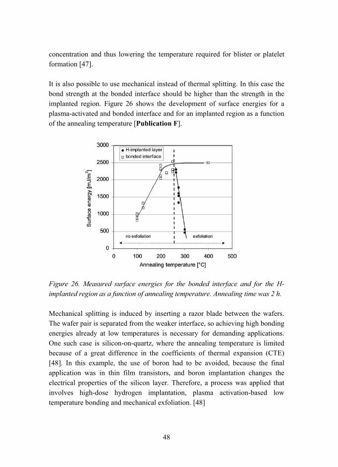
It is also possible to use mechanical instead of thermal splitting. In this case the bond strength at the bonded interface should be higher than the strength in the implanted region. Figure 26 shows the development of surface energies for a plasma-activated and bonded interface and for an implanted region as a function of the annealing temperature [Publication F].
Figure 26. Measured surface energies for the bonded interface and for the H-implanted region as a function of annealing temperature. Annealing time was 2 h.
Mechanical splitting is induced by inserting a razor blade between the wafers. The wafer pair is separated from the weaker interface, so achieving high bonding energies already at low temperatures is necessary for demanding applications. One such case is silicon-on-quartz, where the annealing temperature is limited because of a great difference in the coefficients of thermal expansion (CTE) [48]. In this example, the use of boron had to be avoided, because the final application was in thin film transistors, and boron implantation changes the electrical properties of the silicon layer. Therefore, a process was applied that involves high-dose hydrogen implantation, plasma activation-based low temperature bonding and mechanical exfoliation. [48]

49
After splitting, the surface roughness is 5ñ10 nm RMS and therefore the surface should be polished before device fabrication. The device wafer can be polished and recycled over and over in the process. If the layer needs to be thinned down further, this can be done using thermal oxidation and oxide etching without loosing thickness uniformity. The process is depicted in Figure 27. The Smart Cutô process patent is owned by SOITEC. They fabricate thin film SOI with various thicknesses (50 nm ñ 100 µm) on wafer sizes up to 300 mm.
Figure 27. Smart Cut�-process: a) The device wafer is implanted with hydrogen b) The device wafer is bonded to an oxidized handle wafer, c) Thermal annealing strengthens the bond and induces splitting in the implanted region.
Canon have their own method for fabricating thin film SOI. They grow a porous layer of silicon on the device wafer using a special process, on top of which it is possible to grow epitaxially single crystalline silicon. Once the epitaxial layer is polished, it is bonded to the handle wafer and the layer can be released from the weakest region, which in this case is the porous layer. Their mechanical release process is based on a water jet. [49]
Thin SOI wafers provide many advantages for IC fabrication. The switching speed of circuits fabricated on SOI is increased by 20ñ50% compared to circuits fabricated on a bulk Si wafer. The required operation voltage is lower in ICs on SOI than in ICs on a bulk silicon wafer, which decreases power consumption and chip heating. The circuit packaging density is also increased due to simplification of the lateral and vertical isolation structures.

50
4.1.2 Thick film SOI
Thick film SOI is replacing conventional Si wafers as the start substrate for microelectromechanical systems (MEMS). The advantage of SOI substrates is that the buried oxide layer can be used as sacrificial layer, and by etching it different types of diaphragms, films and beams can be released.
Thick film SOI wafers are made by bonding, grinding and polishing. Before grinding, the edges of the bonded stack are usually ground to avoid edge chipping. The reason for edge chipping is the unbonded area near the edge due to the edge roundness of the bonded wafers. Grinding is usually done in two steps; the first is coarse grinding to remove most of the material, the second is fine grinding (10ñ25 µm removal) to reduce the depth of the grind lines and reduce the sub-surface damage.
A CMP or etching step is used to remove sub-surface damage. The damage layer causes stress to the SOI film and therefore, if not removed, may cause breakage of the MEMS device. CMP is also used to remove the grind lines and create a smooth surface. The CMP causes thickness variation and thus silicon removal with CMP should be minimized.
4.1.3 Intermediate SOI (device layer thickness 2�5 µm)
SOI wafers with thicknesses between 2 and 5 µm are difficult to find, because conventional thinning methods used in thick SOI fabrication cause large procentual thickness variation (0.5 µm TTV is 10% variation for 5 µm SOI layer, 25% for 2 µm SOI layer). Therefore, these layers with intermediate thicknesses are mainly made using either etching thick film SOI with etch stop layers or by growing epitaxially more silicon on thin film SOI.
4.1.4 Strained silicon-on-insulator (sSOI)
Carrier mobility can be improved by having the device layer silicon under tensile stress. [50]. This improves the performance of CMOS circuits fabricated on strained silicon. This improvement can be combined with the advantages of

51
SOI (e.g. reduced junction capacitance) by fabricating strained silicon-on-insulator (sSOI) substrates.
The strain in silicon is typically introduced by epitaxially growing silicon on a material with a larger lattice constant, such as SiGe. sSOI is usually fabricated by first fabricating a SiGe-on-insulator (SGOI) substrate. Three different methods have been reported for SGOI fabrication: SIMOX, Ge-condensation and wafer bonding and thinning [51].
In SIMOX the buried oxide is fabricated by implanting oxygen ions into the substrate, and during subsequent high temperature annealing the implanted oxygen reacts with silicon and forms a buried SiO2 layer. However, this method is only applicable with low Ge concentrations due to thermal instability of SiGe at elevated temperatures [51]. Since the strain-induced hole mobility is expected to continue to improve up to about 30% Ge concentrations, other approaches for SGOI preparation have been developed.
One method for fabricating SGOI substrates with a higher Ge concentration than obtained with SIMOX is the Ge condensation method. Here a low Ge concentration SiGe layer is grown on SOI. When SiGe is exposed to an oxidant, a mixed oxide of SiO2 and GeO2 is formed. At high temperatures, the GeO2 formation is replaced by SiO2 formation and the Ge concentration at the SiGe layer increases, as shown in Figure 28. The oxidation temperature must be kept below the melting point of SiGe alloy. [51]

52
Figure 28. a) Low Ge content SiGe on SOI, x<0.1 b) At high temperature oxidation SiO2 is formed and Ge diffuses into the underlying SiGe, increasing its Ge content, y>x [51].
A third approach to SGOI fabrication is to use wafer bonding combined with a thinning method. In this case the strain-relaxed SiGe layer is grown on a silicon wafer by ultra high vacuum chemical vapour deposition (UHVCVD). The SiGe epilayer is then polished and bonded to an oxidized silicon wafer. Thinning methods are similar to conventional SOI fabrication, including etch back (using SiGe-layer as an etch stop), grinding and polishing as well as ion-implantation based methods.
Once the SGOI substrate is ready, a thin silicon layer is grown on top of it. The silicon is strained due to a larger lattice constant of SiGe. One possible process flow for the fabrication of strained Si-on-SiGe-on-insulator with wafer bonding and ion-cut is depicted in Figure 29 [50].

53
Figure 29. a)The SiGe-on-Si wafer is implanted with hydrogen b) The wafer is bonded to the oxidized Si wafer c) Thermal ion-cut enables SiGe layer transfer from the SiGe-on-Si wafer to the oxidized Si wafer, resulting in an SiGe-on-insulator structure d) Growth of thin Si layer on SGOI substrate. Si is strained due to a lattice mismatch between Si and SiGe. [50]
Having sSOI substrates with a buried SiGe layer, however, poses several challenges to further processing steps. The SiGe-strained Si stack is difficult to make below a thickness of 30 nm. Presence of SiGe layer alters the dopant diffusion and changes the contact metallurgy reactions. Ge may also diffuse into the sSOI layer. Therefore, it would be advantageous to have sSOI wafers without buried SiGe-layer.
Langdo et al. have fabricated SiGe-free sSOI substrates by wafer bonding and layer transfer [52]. They first fabricated a substrate containing a strained Si layer on SiGe-on-Si substrate (Figure 30a). They then implanted hydrogen through the strained Si layer (54 nm thick) into a Si0.68Ge0.32 layer to a depth of ~350 nm below the strained Si. Next the wafer was bonded to the oxidized silicon wafer and annealed to strengthen the bond and induce hydrogen splitting (Figure 30b).

54
The Si0.68Ge0.32 layer film was then removed by a combination of low temperature steam oxidation and dilute HF etching. The final result was SiGe-free strained silicon on the insulator structure (Figure 30c). [52]
Figure 30. Fabrication process for SiGe-free strained Si substrates. a) The SiGe layer is hydrogen implanted through the strained Si layer b) Si on the SiGe-on-Si substrate is bonded to the oxidized silicon wafer and thermal ion-cut is used to transfer the strained silicon layer and part of the SiGe layer c) The SiGe layer is removed by steam oxidation and dilute HF etching. [52]
4.1.5 Cavity SOI
In order to allow greater freedom in MEMS designing, there is increasing interest in SOI wafers with buried structures (cavities, different support structures). A fabrication process for such wafers is presented in Publication C. Fabrication of the pre-patterned SOI wafers requires cavity fabrication on one or both of the wafers before bonding. During cavity fabrication, special care should be taken to keep the surfaces smooth and particle free. It should be emphasized that there are a wide range of different MEMS devices. Different MEMS devices place different demands on pre-patterned SOI wafers concerning cavity location (top, bottom or on both wafers), oxide location (top, bottom, both, on cavity), cavity shape and size, possible support structures (number, shape, size, locations), cavity atmosphere etc. Therefore, the fabrication process for pre-processed SOI also depends on the device. One approach to cavity-SOI fabrication is presented in Figure 31.
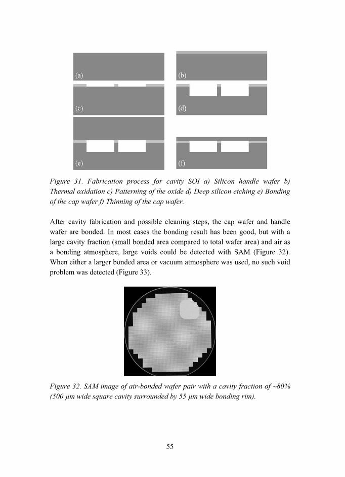
55
Figure 31. Fabrication process for cavity SOI a) Silicon handle wafer b) Thermal oxidation c) Patterning of the oxide d) Deep silicon etching e) Bonding of the cap wafer f) Thinning of the cap wafer.
After cavity fabrication and possible cleaning steps, the cap wafer and handle wafer are bonded. In most cases the bonding result has been good, but with a large cavity fraction (small bonded area compared to total wafer area) and air as a bonding atmosphere, large voids could be detected with SAM (Figure 32). When either a larger bonded area or vacuum atmosphere was used, no such void problem was detected (Figure 33).
Figure 32. SAM image of air-bonded wafer pair with a cavity fraction of ~80% (500 µm wide square cavity surrounded by 55 µm wide bonding rim).

56
Figure 33. a) SAM image of air-bonded wafer pair with a cavity fraction of ~36% (100 µm wide square cavity surrounded by 55 µm wide bonding rim). b) Vacuum-bonded wafer pair with a cavity fraction of ~80% (500 µm wide square cavity surrounded by 55 µm wide bonding rim).
Vacuum bonding resulted in slightly higher bond strength than air bonding [Publication C]. Tests were also performed to study whether small areas can be properly bonded by bonding handle wafers with cavities and small support pillars into the cap wafer and then removing the handle wafer. SEM investigation showed that 100 µm wide pillars were still standing on the cap wafer after handle wafer removal (Figure 34). This means that the support pillar is properly bonded to the cap wafer. Even support pillars with 20 x 20 µm2 area were found to be well bonded.

57
Figure 34. SEM image of 100 µm x 100 µm pillar bonded to the device wafer. The handle wafer is removed with ICP etching.
In cavity SOI wafers, the location of the oxide varies depending on the final application. The oxidation can be done on the cap wafer, the handle wafer before patterning, and the handle wafer after patterning. The first process is straightforward, as the cap wafer is unpatterned and the oxide surface is flat and smooth after thermal oxidation. In the second process care should be taken to avoid roughening of the oxide during cavity fabrication by having a protective layer on top of it, e.g. photoresist. However, in some applications it is desirable to have oxide as well on the bottom of the cavity. The thermal oxidation rate is different in convex and concave corners than on flat surfaces. The oxide profile was measured in the area next to the cavity after cavity fabrication and thermal oxidation with a Veeco Dektak surface profilometer. On these wafers small oxide bumps were detected (width 1ñ5 µm, height 5ñ15 nm) next to the cavity (Figure 35). However, these bumps did not cause voids large enough to be detected with SAM or SEM. [Publication C]

58
Figure 35. Dektak surface profilometer image of oxide shape next to the cavity.
The next step in cavity SOI fabrication is mechanical thinning. The thinning procedure consists of two grinding and one polishing step. The forces present in the grinding and polishing processes press the film in unsupported areas (areas above the cavities) downwards, causing variation in the SOI film thickness [Publication C].
After thinning, the device structure can be defined and released using lithography and ICP etching. Figure 36 shows a MEMS delay line fabricated on a cavity SOI wafer.

59
Figure 36. SEM image of a delay line fabricated on cavity SOI wafer. (Picture courtesy of James Dekker, VTT.)
4.1.6 Multi-layer SOI
Some applications may require substrates with more buried layers than just an insulating oxide layer. For example, in some cases it is advantageous to have a buried conductive layer inside the oxide. A boron-implanted polysilicon layer is one such option. In the process (presented in Figure 37) the cap wafer and the handle wafer are thermally oxidized. The silicon layer is then deposited on the handle wafer using LPCVD. The silicon is deposited in the amorphous state, because polishing of amorphous silicon to the surface roughness required for direct bonding is much easier than polishing of polycrystalline silicon. The amorphous silicon is then ion implanted with boron and polished with a short CMP step (removal ~50 nm). It was decided to carry out ion implantation before CMP, as boron implantation was found to roughen the polished surface from ~1 Å RMS to about ~2.5 Å RMS. The wafers were bonded and annealed at 1100°C for 2 hours.
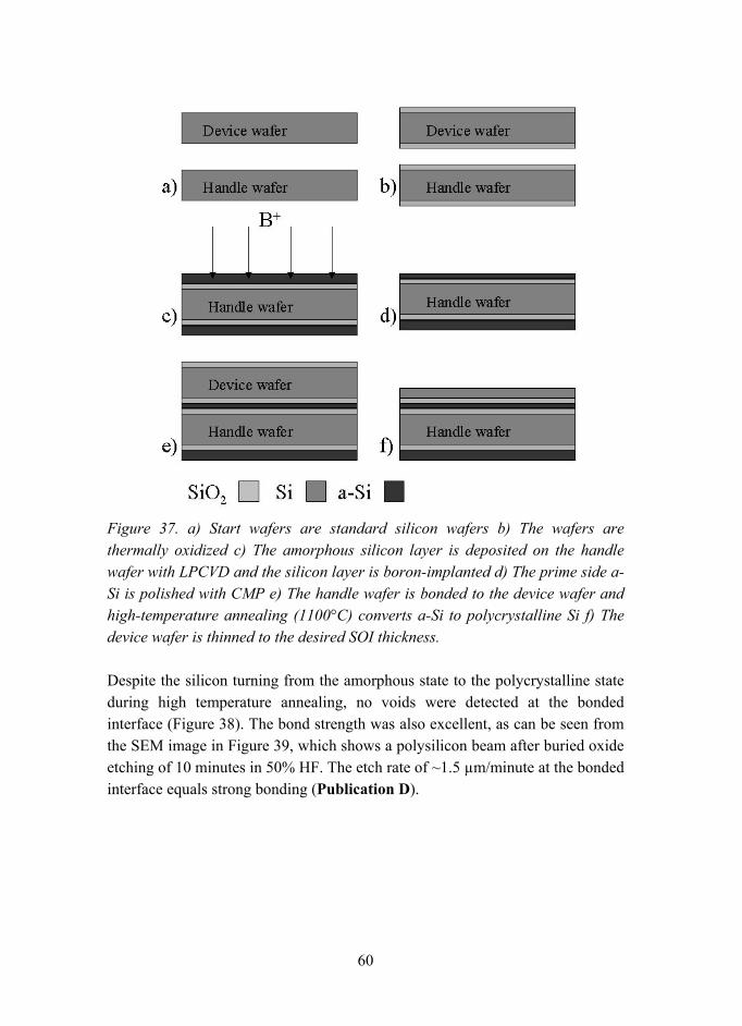
60
Figure 37. a) Start wafers are standard silicon wafers b) The wafers are thermally oxidized c) The amorphous silicon layer is deposited on the handle wafer with LPCVD and the silicon layer is boron-implanted d) The prime side a-Si is polished with CMP e) The handle wafer is bonded to the device wafer and high-temperature annealing (1100°C) converts a-Si to polycrystalline Si f) The device wafer is thinned to the desired SOI thickness.
Despite the silicon turning from the amorphous state to the polycrystalline state during high temperature annealing, no voids were detected at the bonded interface (Figure 38). The bond strength was also excellent, as can be seen from the SEM image in Figure 39, which shows a polysilicon beam after buried oxide etching of 10 minutes in 50% HF. The etch rate of ~1.5 µm/minute at the bonded interface equals strong bonding (Publication D).

61
Figure 38. SAM image of a bonded Si-ox-aSi-ox-Si stack.
Figure 39. SEM image of a polysilicon beam after buried oxide etching (10 min, 50% HF). The etch rate of both oxides is equal and ~1.5 µm/min, which indicates strong bonding.
62
4.2 Heterogeneous integration
Heterogeneous integration means the joining of wafers of different materials. Various materials, such as GaAs, InP, Quartz, Glass, Sapphire, SiC, and GaN have been successfully bonded. In such bonding, the same requirements for smooth and clean surfaces apply, but there are further restrictions in the bonding process. In the bonding of dissimilar materials, there is usually a difference in the coefficients of thermal expansion (CTE), which causes stresses during bond annealing. Therefore, the annealing temperatures are usually limited to lower regions than in silicon-to-silicon bonding. Sometimes polishing of the material to be bonded is too difficult or expensive (e.g. SiC is difficult to polish) and an intermediate layer is needed. A good option is then to use a material with known properties and bonding behaviour. Therefore, most common intermediate layers used in direct bonding are polished CVD-SiO2-layers.
An example of a difficult CTE mismatch is silicon-on-sapphire (SOS) wafers. When bonding silicon to sapphire, the annealing temperature should be kept below 150°C to avoid cracking of the silicon wafer. This causes problems, for example, when trying to make thin film SOS wafers. Low annealing temperature restricts the use of Smart Cutô after the final bonding. For this purpose a temporary wafer bonding has been developed. In this method the device layer is first fabricated on a temporary handle wafer and then transferred to the final substrate. This method requires controlling of the bond strength during both bonding steps to keep the first bonded interface weaker than the second interface. If the difference between the bond strengths is large enough, the layer can be mechanically transferred from one handle wafer to another. The required steps for this method are shown in Figure 40. The methods for controlling the bond strength are explained in more detail in Chapter 5 and Publication E.

63
Figure 40. Principle of temporary wafer bonding for high CTE-mismatched materials integration a) Bonding of desired thin film material to temporary handle wafer b) Thinning of the material with ion-cut or mechanical thinning and polishing to make the surface smooth enough for direct bonding c) Low-temperature bonding of the layer to the final handle wafer d) Delamination at the interface between the thin film and temporary handle wafer.
4.2.1 Compliant substrates
Nowadays heteroepitaxy is a common method for fabricating substrates for electronic and optoelectronic purposes. If the layers have the same lattice constant as the substrate, or if the thickness of the layers is kept below their critical thickness, no defects are formed during growth. If the critical thickness is exceeded, the epitaxial layers relax plastically by forming dislocations at the interface. Lattice and thermal mismatches are the main causes of defect formation [53]. These dislocations cause deterioration of the optical and electrical properties of the structure, therefore the amount of dislocations should be minimized. However, this has proved difficult with standard epitaxy. This problem can be avoided by using a compliant substrate. This kind of substrate should accommodate the misfit by deforming elastically or plastically in a zone localized near its top surface, right below the heteroepitaxial layer [54]. The idea of elastic relief was first introduced by Lo [55]. According to his hypothesis, the template as a whole can shrink or expand by slipping along the weak interface.

64
Several authors have rejected the hypothesis; a more reasonable one is plastic relief of the epitaxial film [56]. In plastic relief the film relaxes by slipping on its crystallographic slip planes, where the slip direction is oblique to the film plane. It may also be that relaxation occurs due to climbing of dislocations instead of slip. However, the final answer regarding the theory behind compliant substrates is still under debate.
There are various methods for fabricating compliant substrates and some of them require wafer bonding. To have an efficient compliant substrate, some criteria should be fulfilled: the layer on which the epitaxy is performed should be as thin as possible, the layer should remain flat and planar and if it is supported, the layer should be free to glide and supporting media should be soft [57].
The first compliant substrates were free-standing thin films, actually GaAs membranes supported at several points (Figure 41a) [58]. However, warping of the film due to stress induced by the deposited epilayer is a serious problem and the method is no longer in use. Another reported freestanding film structure has an InGaAs membrane standing on a central pedestal [59]. However, this structure is fragile and the surfaces are not planar.
Compliant layers when implementing the SOI technique have also been reported (Figure 41b) [60]. In this method the oxide layer is supposed to behave as a viscous layer and a frictionless interface. During epitaxial growth the viscous layer flows, allowing the misfit strain to decrease [61]. As an example of such a compliant substrate, Hansen et al. have reported In0.40Ga0.60As growth on a 10 nm GaAs template on borosilicate glass on a GaAs mechanical host [62]. The viscous intermediate material can also be something else than glass oxide, for example indium.
The most popular option for compliant substrate fabrication has been the use of a twist-bonded layer (Figure 41c). In this method a thin layer of material is transferred to a mechanical host of the same material, but introducing a large twist angle between them. This method was first presented by Ejeckam et al. [63]. The layer is thinned down using either Smart Cutô [43] or an etch-stop layer and etch-back [63, 54]. The twist-bonded substrate is considered to have a weak boundary due to a network of screw dislocations, which can accommodate the slip resulting from growth of a mismatched layer [53].

65
Figure 41. Different compliant substrates a) Free-standing thin film, e.g. GaAs membrane b) Compliant layer on viscous glass c) Twist-bonded layer.
With these different types of compliant substrates, the quality of heteroepitaxially grown layers has increased significantly. Compared with layers grown on ordinary substrates, the density of threatening dislocations has decreased significantly, the relaxation is less or comparable, and the layer thickness is no longer limited to the critical thickness but to a much higher thickness value [57]. While the use of heteroepitaxially grown layers on electrical and optoelectrical applications is increasing, the development of compliant substrates will remain a hot topic in substrate development research.
4.3 Wafer scale packaging
Packaging of MEMS devices is required for various reasons. The sensors are usually delicate components, the operation of which may be sensitive to particles or chemical contaminants. They may also require a specific operation atmosphere (vacuum, inert gas, certain pressure) to function as planned. The encapsulation process should be also cost effective, because nowadays packaging costs can contribute up to 90% of the total device costs. To reduce these costs, the packaging should be done at wafer level, enabling encapsulation of multiple devices on a single run. This can significantly reduce the packaging cost per chip.
66
Wafer-scale packaging is not a new approach in the MEMS industry. The most common methods are anodic bonding and glass frit bonding. These methods, however, have limitations such as high temperature (400ñ600°C) and a large bonding area. These processes also involve metals that are not compatible with ICs sometimes required with the MEMS device. Agilent uses gold seal bonding to encapsulate their devices [24] and Ziptronics uses covalent bonding for wafer-scale encapsulation [42].
Publication B examines methods for direct bonding of a silicon wafer to another silicon wafer containing MEMS devices at low temperature. To achieve strong bonding at low temperatures, plasma activation of wafer surfaces is used before contacting the wafers. The advantages of the plasma-activation based process over glass frit and anodic bonding are a lower process temperature, high throughput, IC compatibility and the possibility to have a small bonding rim. The problem with this method is that the areas to be bonded have to be very smooth and flat, which is usually not the case with processed wafers. Therefore, the device wafer usually needs planarization and/or polishing before direct bonding can take place.
There are three principal steps in the encapsulation of MEMS devices with direct bonding: Planarization and polishing (including surface protection during further processing), bonding itself, and fabrication of electrical contacts into the package.
4.3.1 Planarization and polishing
To make the handle wafer bondable, it needs to be planar and smooth in the areas to be bonded. For this purpose three different approaches were tested: a) covering of the whole handle wafer with thick CVD-oxide, followed by global planarization and smoothening (Figure 42); b) planarization, polishing and protection of the areas to be bonded before actual device fabrication (Figure 43); c) covering of the whole handle wafer with CVD oxide, removal of the oxide from the top of the device and polishing of the elevated oxide areas (Figure 44).

67
Figure 42. a) Device fabrication on oxidized wafer b) Covering of the device with CVD oxide c) Planarization and polishing d) Bonding of cap wafer.
The first proposed method can be done with conventional oxide polishing processes, but it requires a large amount of extra oxide polishing before the step, caused by the buried device, is planarized. Typically the required removal is about twice the height of the hill. By using polishing pads with fixed abrasives, the main part of the removal takes place at the elevated areas and the 800 nm high surface step can be planarized by removing less than 1000 nm of oxide [Publication B].

68
Figure 43. a) Fabrication of conductive path on thermally oxidized Si, CVD oxide deposition, planarization and polishing and deposition and patterning of protective layer b) Device fabrication and contact fabrication from device to conductive path c) Removal of protective layer and aligned bonding to patterned cap wafer d) Thinning of cap wafer for contact opening.
In the second proposed method, the surface of the oxide layer is polished before device fabrication. The areas to be bonded can be polished with a conventional oxide polishing step. The difficult part in this method is to protect the oxide surface during device fabrication so that no roughening of the oxide takes place. The protective layer should also be selectively removable from the top of the oxide. Molybdenum is a good protective layer, for example during release etching with HF, and it can be selectively removed from the oxide surface with mild SC-1 cleaning (NH3:H2O2:H2O solution). If buffered HF is used for release etching, then also standard photoresists can be used for surface protection. The resist can be removed with various solvents and developers without roughening the oxide surface. With complex devices this method is difficult or impossible to use, because it is hard to find a protective material that could withstand all the various process steps and still be easily removable from the oxide surface afterwards.

69
Figure 44. a) Device and conductive path fabrication b) Covering of the device with CVD oxide c) Oxide etching from top of the device and polishing of elevated oxide areas d) Bonding to cap wafer.
The third option is to fabricate the device first, cover it with CVD oxide, remove it from the top of the device, and then polish the areas to be bonded. With typical polishing processes the problem is rounding of the corners of the oxide ìwallsî, which especially with a narrow bonding rim areas drastically reduce the area to be bonded (Figure 45b&c). By again implementing the fixed abrasive polishing process, the elevated oxide areas can be polished without detectable edge rounding (Figure 45d).

70
Figure 45. Surface profiles of elevated oxide areas a) After patterning b) After conventional oxide polishing process c) Oxide pillar profile after conventional oxide CMP d) Oxide pillar profile after fixed abrasive polishing process.
The encapsulation process needs to be decided upon already when designing the MEMS and its fabrication process.
4.3.2 Direct bonding of MEMS wafer
Direct bonding of wafers containing MEMS devices must in most cases be carried out at low temperature. The temperature of 1100°C needed for the high-temperature bonding process is too high for possible metallizations and other temperature sensitive parts, and also causes outgassing (and void formation) from the CVD oxides. Therefore, plasma activation should be used for both wafer surfaces to achieve strong bonding already at 200°C. In cases where the cap wafer is patterned, aligned bonding should be used.

71
The main thing to remember in direct bonding of wafers containing MEMS is the same as with any other direct bonding processes: the areas to be bonded must be smooth and clean. Therefore, it is important to highlight again the need for good CMP processes and the importance of having particle-free processes.
4.3.3 Fabrication of electrical contacts
In Publication B two different methods for fabrication of electrical contacts are presented. The first possibility is to use a patterned cap wafer which contains wells for contact opening. The wells are aligned during bonding above the contact pads, and during cap wafer thinning the wells are opened and a path to the contact pads is created (Figure 43). The encapsulated device can then be contacted to the next level, for example by wire bonding (Figure 46).
Figure 46. Contact fabrication with wire bonding for encapsulated device, continuation of the process presented in Figure 43.
The second approach is to use a dicing saw for the contact opening. The bonded cap wafer is first thinned down to <100 µm thickness. Next the v-shaped dicing blade is used to cut through the remaining handle wafer, slightly penetrating the contact pads. After this, a layer of conductive material, e.g. molybdenum, is deposited onto the v-groove and patterned (Figure 47). Then, for example, solder bumps can be grown on top of the cap wafer to make the final contacts to the next level.

72
Figure 47. Contact fabrication with an encapsulated device, continuation of the process presented in Figure 44. a) Encapsulated device b) Thinning of the handle wafer c) V-groove sawing through the handle wafer and contact pads d) Conductive material deposition into the groove, patterning and solder bumping.

73
5. Temporary wafer bonding Temporary wafer bonding means bonding of wafers to a temporary substrate so that they can easily be released afterwards. The principle of the method is presented in Figure 48 and explained in more detail in Publication E. The main principle of the method is that the crack propagates on the weakest interface. Therefore, if the bonding between the temporary holder wafer and the thin film is weaker than between the thin film and the final handle wafer, the film can be transferred to the final substrate. In practice, the difference should be significant (> 500 mJ/m2) to avoid ìjumpingî of the crack from one interface to another.
Figure 48. Principle of temporary wafer bonding a) Bonding of the desired thin film material to the temporary handle wafer b) Thinning of the material with ion-cut or mechanical thinning, and polishing to make the surface smooth enough for direct bonding c) Low-temperature bonding of the layer to the final handle wafer d) Delamination at the interface between the thin film and the temporary handle wafer.
The use of a temporary handle wafer is advantageous in many cases, such as wafer thinning and heterogeneous integration. For example, the quality of ion-cut silicon-on-glass (SOG) layers can be improved by removing ion implantation induced crystalline damage from the silicon film with high temperature annealing (at >1000°C). However, the glass substrate cannot withstand temperatures over 600°C and annealing before bonding is out of the question

74
because of the blistering effect. Therefore, the annealing should be done while the thin film is on a temporary handle (Si) wafer.
Temporary wafer bonding is also a usable method in fabrication of silicon-on-sapphire (SOS) wafers. Coefficients of thermal expansion (CTE) vary between silicon and sapphire so that the bonded silicon-sapphire wafer pair starts to break at temperatures over 150°C. However, the ion-cut requires annealing temperatures of ~200°C even if boron implantation and mechanical delamination are used [46]. The SOS wafer can be fabricated by first bonding the implanted silicon wafer to the oxidized silicon wafer without plasma activation, then doing a thermal ion-cut at 500°C. The transferred Si-layer is then polished to reduce the surface roughness from a split roughness of ~3 nm RMS to ~1 Å RMS. On a sapphire wafer, the PECVD oxide layer should be deposited to avoid void formation during bonding. PECVD oxide should also be polished to enable direct bonding. After ion-cut annealing, the bond strength of the temporary bonding is <1000 mJ/m2. By using plasma activation on both surfaces and long annealing at 120°C, bonding between the sapphire and silicon layer could be made much stronger than the temporary bonding. After mechanical delamination, the surface roughness of the transferred layer was ~1 Å RMS, which is close to the surface roughness of the donor wafer at the start of the process. A thin film SOS wafer is shown in Figure 49.
Figure 49. Picture of thin Si layer on a sapphire wafer.

75
The third application would be the fabrication of cavity SOI wafers (Figure 50). As mentioned in chapter 4.5.1, mechanical thinning induces thickness variation in diaphragms above cavities. Therefore, it would be advantageous (especially with thin diaphragm thicknesses) to do the thinning while the SOI layer is on the temporary substrate. Once the SOI layer is thinned to desired thickness, it is bonded to the patterned wafer and the temporary handle is removed by debonding.
Figure 50. Temporary wafer bonding for cavity SOI fabrication a) Fabrication of SOI wafer with weak bonded interface b) Bonding of temporary SOI wafer to cavity wafer c) Mechanical delamination for removal of the temporary handle.
With this method it is also possible to carry out double side processing on the SOI layer. In this case one side of the SOI layer is processed while it is bonded to the temporary substrate. After bonding and debonding, another side of the SOI layer can also be processed. It is also possible to stack many processed SOI layers on the same handle wafer. [Publication E, 64]
5.1 Temporary wafer bonding using impurity outgassing of CVD oxides
Impurity outgassing of CVD oxides can be used for temporary wafer bonding. As mentioned in the chapter on bonding of CVD oxides, trapped impurities start to outgas when the bond annealing temperature exceeds the film deposition

76
temperature. Use of this behaviour in temporary wafer bonding was tested by bonding a PECVD oxide layer to a silicon wafer using plasma activation and annealing at 200°C. After this bonding procedure, the bond is strong. Then the cap silicon wafer was thinned down to a thickness of 20 µm by grinding and polishing. After polishing, the surface roughness of the SOI layer was low enough to enable good bonding. This SOI wafer was then bonded to a thermally oxidized wafer with plasma activation and the wafer stack was annealed at 500°C. At this temperature, the first made bonded interface weakens due to impurity outgassing (Figure 8b) while the second interface gets stronger. After annealing, a razor blade was inserted between the wafers and the crack propagated on the weaker PECVD oxide / silicon interface. After complete separation the 20 µm SOI layer was successfully transferred to another substrate. The new SOI wafer had some residual PECVD oxide on the surface due to crack propagation partly inside the CVD oxide layer. After short a HF dip the oxide residues were removed and the silicon surface was found to be smooth (~1Å RMS).
5.2 Temporary wafer bonding using surface roughening
The requirements for spontaneous direct bonding to take place are smooth and clean surfaces. The surface roughness limit is ~1 nm RMS and usually the silicon and oxide surfaces have a surface roughness of 1ñ2 Å RMS. Publication E describes how increasing the surface roughness within the limits of spontaneous bonding affects the bond strength. Similar results have been published by Moriceau et al. [64]
The optimal target would be to have a controlled surface energy (of 700ñ1200 mJ/m2) for a temporarily bonded wafer pair after annealing at temperatures ranging from 200°C to 1100°C. This would enable thermal ion-cut at low temperatures and removal of the ion-implantation induced crystalline damage with high temperature annealing before moving the thin film to the final substrate. If the bond strength is below 500 mJ/m2 at the thermal ion-cut temperature, instead of a thermal cut blistering and debonding will occur.
The experiments focused mainly on roughening of thermally grown oxide with plasma etching. After several tests, the best process for roughening the oxide

77
surface was found to be 30s CHF3 plasma etching, which resulted in a surface roughness of ~8 Å RMS (Figure 51).
Figure 51. AFM images of a) as grown thermal oxide (RMS ~2 Å) and b) roughened thermal oxide (RMS ~8 Å).
Figure 52 presents measured surface energies for roughened and bonded SiO2 wafers after annealing at different temperatures. Roughening of surfaces has a clear influence on the bonding energy and the bond strength remains at a level still debondable after annealing at 1100°C. However, with roughened surfaces the bond strength at temperatures < 500°C is not sufficient for thermal ion-cut.

78
Figure 52. Bond strength as a function of annealing temperature for oxide-oxide wafer pairs with and without surface roughening. Annealing time was 2 h.
To improve bond strength at low annealing temperatures, plasma activation was combined with surface roughening. The plasma activation of the roughened surface seemed to remove the influence of the roughening somewhat, and the bond strength at high temperatures was similar or higher to that in reference samples (Figure 53). By plasma-activating one wafer and roughening the other, the desired results were obtained enabling ion-cut at 400°C (bond strength ~500 mJ/m2) and debonding after high temperature annealing (~1200 mJ/m2).

79
Figure 53. Measured bond strengths for oxide-oxide wafer pairs as a function of annealing temperature after different roughening and plasma activation procedures. Annealing time was 2 h.

80
6. Summary The purpose of this work was to study silicon direct bonding processes and evaluate the influence of different pre-bonding treatments on the bond quality. The main focus was on studying the effect of plasma activation before bonding on the bond strength. The influence of other pre-bonding treatments such as chemical-mechanical polishing (CMP), lithographical surface patterning and surface roughening was studied while developing bonding processes for various applications. These applications included heterogeneous integration for fabrication of silicon-on-glass (SOG) and silicon-on-sapphire (SOS) substrates, bonding of patterned wafers for fabrication of SOI substrates with buried cavities, and bonding of wafers with MEMS devices for wafer scale packaging.
The plasma-activation based bonding process reduces the required annealing temperature to achieve strong silicon to thermal oxide bonding from 1100°C to <200°C. Plasma is assumed to create a porous layer on the oxide surface, which helps the water diffuse out from the bonded interface at low temperature. The plasma activation effect can be lost by excess SC-1 cleaning after activation.
The plasma activation-based bonding process has been found to be a suitable method for MEMS encapsulation at wafer level. Covering the wafer with LPCVD oxide and using it as an intermediate bonding layer was found to be a viable method for encapsulation. Suitable CMP processes were found for LPCVD oxide planarization and polishing. By using a protective layer above areas to be bonded during further processing, surface roughening could be avoided. Two methods were developed for fabrication of electrical contacts in the package. Contact pad opening by grinding or sawing enables electrical contact to the package without losing the hermeticity of the package.
Patterning, bonding and mechanical thinning is a viable method for fabricating SOI wafers with buried cavities. Such new substrates enable fabrication of MEMS components difficult or impossible to fabricate on conventional Si or SOI wafers.
Bond strength is usually measured with the crack opening method or a chevron test. The former requires a place for blade insertion, and is therefore unsuitable for thinned or diced samples. It also has problems measuring high bond strengths

81
or fragile samples due to sample breakage during measurement. The latter method is accurate but requires pre-patterning before bonding and is therefore time-consuming. The HF etching test was found to be a suitable method for measuring bond strength from ready-made SOI, small samples or small bonded areas. In the method the buried oxide is etched in HF and the etched distance is measured. In direct bonding of hydrophilic silicon, the bond strength was found to be logarithmically dependent on the bond strength. The etched distance can be measured by cross-sectional SEM or IR microscopy.
The mechanical exfoliation of hydrogen implantation and bonded Si is a suitable method for fabrication of thin film silicon-on-insulator and silicon-on-glass substrates. In mechanical exfoliation the crack propagates on the weakest interface, therefore it is necessary to achieve a high bond strength at low temperature by using plasma activation. With this method the mechanical transfer of hydrogen-implanted Si is possible after annealing at 200°C. The strength of the implanted layer is dependent not only on the hydrogen dose, but also on crystalline orientation and boron doping. High boron doping (implantation dose of 3e15 cm-2) combined with hydrogen implantation was found to decrease the required annealing temperature for mechanical exfoliation of about 80°C compared to a sample with hydrogen implantation only.
Controlling of the bond strength is possible with different surface preparations. By slightly increasing the surface roughness of wafers to be bonded, the bond strength can be limited to a level that is still mechanically debondable after high temperature annealing (1100°C). For example, the crystalline damage due to hydrogen implantation in ion-cut Si layers could be removed by high temperature annealing on temporary substrate before transferring the Si film onto a temperature-sensitive final substrate.

82
References
1. J. Haisma, G. A. C. M. Spierings. Contact bonding, including direct-bonding in a historical and recent context of materials science and technology, physics and chemistry ñ Historical review in a broader scope and comparative outlook. Materials Science and Engineering R, Vol. 37, (2002), pp. 1ñ60.
2. Q.-Y. Tong, and U. Gösele. Semiconductor Wafer Bonding. John Wiley & Sons, Inc. (1999).
3. A. Plössl, and G. Kräuter. Wafer direct bonding: tailoring adhesion between brittle materials. Materials Science and Engineering, Vol. R25, (1999), pp. 1ñ88.
4. S. Bengtsson, and P. Amirfeiz. Room temperature wafer bonding of silicon, oxidized silicon and crystalline quartz. Journal of Electronic Materials, Vol. 29, No. 7, (2000), pp. 909ñ915.
5. S. N. Farrens, J. R. Dekker, J. K. Smith, and B. E. Roberds. Chemical free room temperature wafer to wafer direct bonding. Journal of the Electrochemical Society, Vol. 142, No. 11, (1995), pp. 3949ñ3955.
6. G. Kräuter, A. Schumacher, and U. Gösele. Low temperature silicon direct bonding for application in micromechanics: bonding energies for different combinations of oxides. Sensors and Actuators A, Vol. 70, (1998), pp. 271ñ275.
7. M. Reiche, K. Gutjahr, D. Stolze, D. Burczyk, and M. Petzold. The effect of a plasma pretreatment on the Si/Si bonding behaviour. In Semiconductor Wafer Bonding: Science, Technology and Applications IV, edited by, U. Gösele, H. Baumgart, T. Abe, C. Hunt, S. Iyer. The Electrochemical Society (1997). Pp. 437ñ444.

83
8. S. Senz, A. Reznicek, T. Akatsu, G. Kästner, R. Scholtz, and U. Gösele. UHV-bonding: Electrical characterization of interfaces and application to magnetoelectronics. In Semiconductor Wafer Bonding: Science, Technology and Applications VI, edited by H. Baumgart, C. Hunt, S. Bengtsson, T. Abe. The Electrochemical Society (2001). Pp. 48ñ61.
9. A. Reznicek, S. Senz, O. Breitenstein, R. Scholtz, and U. Gösele. Electrical and structural investigation of bonded silicon interfaces. In Semiconductor Wafer Bonding: Science, Technology and Applications VI, edited by H. Baumgart, C. Hunt, S. Bengtsson, T. Abe. The Electrochemical Society (2001). Pp. 48ñ61.
10. Q.-Y. Tong, Q. Gan, G. Hudson, G. Fountain, P. Enquist, R. Scholtz, and U. Gösele. Low-temperature hydrophobic silicon wafer bonding. Applied Physics Letters, Vol. 83, No. 23, (2003), pp. 4767ñ4769.
11. A. Paskaleva, and E. Atanassova. Damage in thin SiO2-Si structures induced by RIE-mode nitrogen and oxygen plasma. Solid-State Electronics, Vol. 42, No. 5, (1998), pp. 777ñ784.
12. D. Pasquariello, M. Lindeberg, C. Hedlund, and K. Hjort. Surface energy as a function of self-bias voltage in oxygen plasma wafer bonding. Sensors and Actuators A: Physical, Vol. 82, Issues 1ñ3, (2000), pp. 239ñ244.
13. H. Moriceau, F. Rieutord, C. Morales, S. Sartori, and A. M. Charvet. Surface plasma activation before direct wafer bonding: a short review and recent results. In Semiconductor Wafer Bonding: Science, Technology and Applications VIII, edited by, K. D. Hobart, S. Bengtsson, H. Baumgart, T. Suga, C. E. Hunt. The Electrochemical Society (2005). Pp. 34ñ49.
14. A. Paskaleva, and E. Atanassova. Electrical stress and plasma-induced traps in SiO2. Microelectronics Reliability, Vol. 40, (2000), pp. 933ñ940.
15. S. Weichel. Silicon to silicon wafer bonding for microsystem packaging and formation. Ph. D. Thesis, Mikroelektronik Centret, Technical University of Denmark (2000).

84
16. P. Amirfeiz, S. Bengtsson, M. Bergh, E. Zanghellini, and L. Börjesson. Formation of silicon structures by plasma-activated wafer bonding. Journal of the Electrochemical Society, Vol. 147, No. 7, (2000), pp. 2693ñ2698.
17. H. Luoto, T. Suni, K. Henttinen, and M. Kulawski. Direct bonding of thick film polysilicon to glass substrates. In Semiconductor Wafer Bonding: Science, Technology and Applications VIII, edited by, K. D. Hobart, S. Bengtsson, H. Baumgart, T. Suga, C. E. Hunt. The Electrochemical Society (2005). Pp. 194ñ204.
18. G. Wallis, and D. I. Pomerantz. Field assisted glass-metal sealing. Journal of Applied Physics, Vol. 40, No. 10, (1969), pp. 3946ñ3949.
19. H. Jakobsen, A. Lapadatu, and G. Kittilsland. Anodic bonding for MEMS. In Semiconductor Wafer Bonding: Science, Technology and Applications VI, edited by H. Baumgart, C. Hunt, S. Bengtsson, T. Abe, The Electrochemical Society (2001). Pp. 243ñ253.
20. P. Enoksson, C. Rusu, A. Sanz-Velasco, M. Bring, A. Nafiri, and S. Bengtsson. Wafer bonding for MEMS. In Semiconductor Wafer Bonding: Science, Technology and Applications VIII, edited by, K. D. Hobart, S. Bengtsson, H. Baumgart, T. Suga, C. E. Hunt. The Electrochemical Society (2005). Pp. 157ñ172.
21. C. T. Pan, P. J. Cheng, M. F. Chen, and C. K. Yen. Intermediate wafer level bonding and interface behavior. Microelectronics Reliability, Vol. 45, (2005), pp. 657ñ663.
22. F. Niklaus, H. Andersson, P. Enoksson, and G. Stemme. Low temperature full wafer adhesive bonding of structured wafers. Sensors and Actuators A, Vol. 91, (2001), pp. 235ñ241.
23. F. Niklaus, R. J. Kumar, J. J. McMahon, J. Yu, J.-Q. Lu, T. S. Cale, and R. J. Gutmann. Adhesive wafer bonding using partially cured benzocyclobutene for three-dimensional integration. Journal of the Electrochemical Society, Vol. 153, No. 4, (2006), pp. G291ñG295.

85
24. F. S. Geefay. Method for sealing a semiconductor device and apparatus embodying the method. US Pat. 6,836,013 (2004).
25. H. A. C. Tilmans, M. D. J. Van der Peer, and E. Beyne. The indent reflow sealing (IRS) technique ñ a method for the fabrication of sealed cavities for MEMS devices. Journal of Microelectromechanical Systems, Vol. 9, No. 2, (2000), pp. 206ñ217.
26. Y. Tao, A. P. Malshe, and W. D. Brown. Selective bonding and encapsulation for wafer-level vacuum packaging of MEMS and related micro systems. Microelectronics Reliability, Vol. 44 (2004), pp. 251ñ258.
27. J. Kim, and C. C. Lee. Fluxless wafer bonding with Sn-rich Sn-Au dual-layer structure. Materials Science and Engineering A, Vol. 417, (2006), pp. 143ñ148.
28. R. Knechtel. Glass frit bonding: an universal technology for wafer level encapsulation and packaging. Microsystem Technologies Vol. 12, (2005), pp. 63ñ68.
29. R. Howland, and L. Benatar. A practical guide to scanning probe microscopy. Park Scientific Instruments (1993).
30. J. Schmit, P. Unruh, and D.-S. Wan. Optical profiler for surface characterization and film thickness measurement. White paper, Veeco Instruments Inc. http://www.veeco.com/pdf/Optical_Library/Surface_Characterization.pdf
31. W. P. Maszara, G. Goetz, A. Caviglia, and J. B. McKitterick. Bonding of silicon wafers for silicon-on-insulator. Journal of Applied Physics, Vol. 64, No. 10, (1988), pp. 4943ñ4950.
32. Ö. Vallin, K. Jonsson, and U. Lindberg. Adhesion quantification methods for wafer bonding. Materials Science and Engineering R, Vol. 50, No. 4ñ5, (2005), pp. 109ñ165.

86
33. T. Abe, M. Nakano, T. Itoh. Silicon wafer bonding process technology for SOI structures. In Proceedings of the Fourth International Symposium on Silicon-On-Insulator Technology and Devices, edited by Dennis N. Schmidt. The Electrochemical Society (1990). Pp. 61ñ71.
34. J. Bagdahn, A. Plößl, M. Wiemer, and M. Petzold. Measurement of local strength distribution of directly bonded silicon wafers using the micro-chevron-test. In Semiconductor Wafer Bonding: Science, Technology and Applications V, edited by C. E. Hunt, T. Abe, H. Baumgart, and U. Gösele. The Electrochemical Society (1999). Pp. 218ñ223.
35. J. Bagdahn, M. Bernasch, and M. Petzold. Influence of the frequency on fatique of directly wafer-bonded silicon. Microsystem Technologies, Vol. 12, No. 5, (2006), pp. 430ñ435.
36. D. Bollmann, C. Landesberger, P. Ramm, and K. Haberger. Analysis of wafer bonding by infrared transmission. Japanese Journal of Applied Physics, Vol. 35, (1996), pp. 3807ñ3809.
37. W.P. Maszara. Silicon-on-Insulator by Wafer Bonding: A Review., Journal of The Electrochemical Society, vol. 138, (1991), pp. 341ñ347.
38. Web page of Phoseon Technology. www.phoseon.com
39. Z. Yu, and S. Boseck. Scanning acoustic microscopy and its applications to materials characterization. Reviews of Modern Physics, Vol. 67, No. 4, (1995), pp. 863ñ891.
40. N. Miki, X. Zhang, R. Khanna, A. A. Ayón, D. Ward, and S. M. Spearing. Multi-stack silicon-direct wafer bonding for 3D MEMS manufacturing. Sensors and Actuators A, Vol. 103, (2003), pp. 194ñ201.
41. L. Di Cioccio, B. Biasse, M. Kostrzeva, M. Zussy, J. Dechamp, B Charlet, M. Vinet, J. M. Fedeli, T. Poiroux, C. Lagahe-Blanchard, B. Aspar, P. Regreny, and N. Kernevez. Recent results on advanced molecular wafer bonding technology for 3D integration on silicon. In Semiconductor Wafer Bonding: Science, Technology and Applications VIII, edited by, K. D.

87
Hobart, S. Bengtsson, H. Baumgart, T. Suga, C. E. Hunt. The Electrochemical Society (2005). Pp. 280ñ287.
42. P. M. Enquist, Q.-Y. Tong, G. G. Fountain, and R. Markunas. Wafer bonding hermetic encapsulation. US Pat. US2005009246 (2005).
43. M. Bruel. Silicon on insulator material technology. Electronics Letters, Vol. 31, No. 14, (1995), pp. 1201ñ1202.
44. A. Nurmela, K. Henttinen, T. Suni, and I. Suni. Influence of hydrogen dose and boron doping on the ion cutting of Si. Surface and Interface Analysis, Vol. 35, (2003), pp. 757ñ759.
45. T. Höchbauer, A. Misra, M. Nastasi, K. Henttinen, T. Suni, I. Suni, S.S. Lau, and W. Ensinger. Comparison of thermally and mechanically induced Si layer transfer in hydrogen-implanted Si wafers. Nuclear Instruments and Methods in Physics Research Section B: Beam Interactions with Materials and Atoms. Vol. 216, (2004), pp. 257ñ263.
46. A. Nurmela, K. Henttinen, T. Suni, A. Tolkki, and I. Suni. Ion beam studies of hydrogen implanted Si wafers. Nuclear Instruments and Methods in Physics Research Section B: Beam Interactions with Materials and Atoms. No. 219ñ220, (2004), pp. 747ñ750.
47. T. Höchbauer, K. C. Walter, R. B. Schwartz, M. Nastasi, R. W. Bower, and W. Ensinger. The influence of boron ion implantation on hydrogen blister formation in n-type silicon. Journal of Applied Physics, Vol. 86, No. 8, (1999), pp. 4176ñ4183.
48. X. Shi, K. Henttinen, T. Suni, I. Suni, and M. Wong. Charasteristics of transistors fabricated on silicon-on-quartz prepared by using a mechanically initiated exfoliation technique. IEEE Electron Device Letters, Vol. 26, No. 9, (2005), pp. 607ñ609.
49. K. Sakaguchi, K. Yanagita, H. Kurisu, H. Suzuki, K. Ohmi, and T. Yonehara. ELTRAN by water-jet splitting in stress-controlled porous Si. In

88
Proceedings of the 1999 IEEE International SOI Conference, IEEE (1999). Pp. 110ñ111.
50. L. Huang, J. O. Chu, S. A. Goma, C. P. DíEmic, S. J. Koester, D. F. Canaperi, P. M. Mooney, S. A. Cordes, J. L. Speidell, R. M. Anderson, and H.-S. P. Wong. Electron and hole mobility enhancement in strained SOI by wafer bonding. IEEE Transactions on Electron Devices, Vol. 49, No. 9, (2002), pp. 1566ñ1571.
51. G. Taraschi, A. J. Pitera, and E. A. Fitzgerald. Strained Si, SiGe, and Ge on-insulator: review of wafer bonding fabrication techniques. Solid-State Electronics, Vol 48, (2004), pp. 1297ñ1305.
52. T. A. Langdo, M. T. Currie, A. Lochtefeld, R. Hammond, J. A. Carlin, M. Erdtmann, G. Braithwaite, V. K. Yang, C. J. Vineis, H. Badawi, and M. T. Bulsara. SiGe-free strained Si on insulator by wafer bonding and layer transfer. Applied Physics Letters, Vol. 82, No. 24, (2003), pp. 4256ñ4258.
53. A. S. Brown, W. A. Doolittle, N. M. Jokerst, S. Kang, S. Huang, and S. W. Seo. Heterogeneous materials integration: Compliant substrates to active device and materials packaging. Materials Science and Engineering B, Vol. 87, (2001), pp. 317ñ322.
54. G. Patriarche, C. Mériadec, G. LeRoux, C. Depardis, I. Sagnes, J.-C. Harmand, and F. Glas. GaAs/GaAs twist-bonding for compliant substrates: interface structure and epitaxial growth. Applied Surface Science, Vol. 164, (2000), pp. 15ñ21.
55. Y. H. Lo. New approach to grow pseudomorphic structures over the critical thickness. Applied Physics Letters, Vol. 59, No. 6, (1991), pp. 2311ñ2313.
56. G. Kästner. Heteroepitaxy on compliant substrates: relaxation of misfit stress at low critical film thickness. Physica Status Solidi A, Vol. 195, No. 2, (2003), pp. 367ñ374.
57. A. Bourret. Compliant substrates: a review on the concept, techniques and mechanism. Applied Surface Science, Vol. 164, (2000), pp. 3ñ14.

89
58. C. L. Chua, W. Y. Hsu, C. H. Lin, G. Christenson, and Y. H. Lo. Overcoming the pseudomorphic critical thickness limit using compliant substrates. Applied Physics Letters, Vol. 64, No. 26, (1994), pp. 3640ñ3642.
59. A. M. Jones, J. L. Jewell, J. C. Mabon, E. E. Reuter, S. G. Bishop, S. D. Roh, and J. J. Coleman. Long-wavelength InGaAs quantum wells grown without strain-induced warping on InGaAs compliant membranes above a GaAs substrate Applied Physics Letters, Vol. 74, No. 7, (1999), pp. 1000ñ1002.
60. A. R. Powell, S. S. Iyer, and F. K. LeGoues. New approach to the growth of low dislocation relaxed SiGe material. Applied Physics Letters, Vol. 64, No. 14, (1994), pp. 1856ñ1858.
61. H. Y. Jiang, and L. H. He. Morphological stability of films deposited on an SOI substrate. Journal of Crystal Growth, Vol. 262, (2004), pp. 28ñ34.
62. D. M. Hansen, P. D. Moran, K. A. Dunn, S. E. Babcock, R. J. Matyi, and T. F. Kuech. Development of a glass-bonded compliant substrate. Journal of Crystal Growth, Vol. 195, (1998), pp. 144ñ150.
63. F. E. Ejeckam, Y. H. Lo, S. Subramanian, H. Q. Hou, and B. E. Hammons. Lattice engineered compliant substrate for defect-free heteroepitaxial growth. Applied Physics Letters,Vol. 70, No. 13, (1997), pp. 1685ñ1687.
64. H. Moriceau, O. Rayssac, B. Aspar, and B. Ghyselen. The bonding energy control: an original way to debondable substrates. In Semiconductor Wafer Bonding: Science, Technology and Applications VII, edited by S. Bengtsson, H. Baumgart, C. E. Hunt, T. Suga. The Electrochemical Society (2003). Pp. 49ñ56.

PUBLICATION A
Effects of Plasma Activation on Hydrophilic Bonding of Si and SiO2
Journal of The Electrochemical Society, Vol. 149, No. 6, (2002), pp. G348–G351.
Reprinted by permission of ECS – The Electrochemical Society.
Journal of The Electrochemical Society, 149 ~6! G348-G351~2002!0013-4651/2002/149~6!/G348/4/$7.00 © The Electrochemical Society, Inc.
G348
Effects of Plasma Activation on Hydrophilic Bonding of Siand SiO2
T. Suni,a,z K. Henttinen,a I. Suni,a and J. Makinenb
aV T T Electronics, Microelectronics Center, FIN-02150 Espoo, FinlandbOkmetic Oyj, FIN-01510 Vantaa, Finland
Low-temperature bonding of Si wafers has been studied utilizing reactive ion etching-mode plasma activation. The hydrophilic Siand thermally oxidized Si wafers were exposed to N2 , Ar, or O2 plasma prior to bonding in air or vacuum. After plasma treatmentthe wafers were cleaned in RCA-1 solution and/or deionized water. Strong bonding was achieved at 200°C with all the investi-gated plasma gases, if proper bonding and cleaning procedures were used. Extended RCA-1 cleaning deteriorated the bondstrength, but a short cleaning improved bonding. We found that the activation of the thermal oxide has a larger influence on thebond strength than the activation of the native oxide surface in Si/oxide wafer pairs. We suggest that the plasma treatment inducesa highly disordered surface structure, which enhances the diffusion of the water from the bonded interface. As a result of theplasma exposure the number of the surface OH groups is greatly increased enabling strong bonding at a low temperature.© 2002 The Electrochemical Society.@DOI: 10.1149/1.1477209# All rights reserved.
Manuscript submitted October 2, 2001; revised manuscript received December 21, 2001. Available electronically April 25, 2002.
todaltrors
voInex, itts
an
t i
-hilds
ntheheanexecceedth
ione
t-us, aultThfie
in
de
od,ning
-of
-be
thet 30esetweenriedfers
pftererederns at
larfor
ples
is-
mea-pe
gat-e/Siwe
afersbse-ir.
afterFor
ongond
Direct bonding of hydrophilic silicon wafers can be appliedthe fabrication of silicon-on-insulator~SOI! structures and advancemicroelectromechanical and optical devices. Wafer bonding usurequires high-temperature annealing above 1000°C to achieve sbonding between the wafers. When bonding preprocessed wafeis essential to restrict the annealing temperature in order to aundesirable changes and reactions in the substrate structures.case of materials with different thermal expansion coefficientscessive stresses may arise in the bonded wafer pair. Thereforemandatory to find a low-temperature bonding process that resulstrong bonding at temperatures below 400°C.
It has been reported that strong hydrophilic bonding with Si cbe achieved at a low annealing temperature~,400°C! by exposingthe wafers to a low pressure plasma prior to the bonding.1-3 Alter-natively, surfaces can also be activated with ion bombardmenvacuum.4 The plasma of various gases, including O2 and Ar, havebeen found to yield similar results.1,3 Infrared spectroscopic measurements have confirmed that the bond strengthening in hydropbonding of Si is due to the formation of covalent siloxane bon~Si-O-Si! at the bonded interface.3,5 This reaction which involvesdissociation of silanol groups at the interface can take place everoom temperature. The resulting bond strength is limited bynumber of silanol groups available for the bonding reaction. Furtbonding only occurs at higher temperatures via plastic flowdistortion of the silica tetrahedra. Ion bombardment by plasmaposure or by incident ion beam is known to create structural defon a Si surface.6 The particles and ions impinging on a Si surfaalso have a charging effect.6 It has been proposed that the disordersurface structure is responsible for the increased reactivity ofsurface.1 Farrenset al. have suggested that the increased oxidatrate ~Si-O-Si bond formation! at the bonded interface is due to thplasma induced surface charge.2 Amirfeiz et al. found no evidenceto substantiate this hypothesis.3 They suggested that plasma treament creates a porous surface structure which enhances the diffity of water molecules from the bonded interface. In summarynumber of experiments with varying, sometimes conflicting, reshave been published on plasma-activated Si wafer bonding.suggests that the effects of plasma activation are not fully clariyet.
We have studied the influence of various plasma and bondparameters on the hydrophilic bonding of Si and SiO2 using alter-native surface treatment procedures prior to bonding. The bon
z E-mail: [email protected]
A/1
lyngit
idthe-is
in
n
ic
at
rd-ts
e
iv-
sisd
g
d
interface strength was measured with the crack-opening meth1
and the voids at the bonded interface were studied with scanacoustic microscopy~SAM!.
Experimental
In the experiments,100& oriented p-type Czochralski grown silicon wafers with a diameter of 100 mm were used. The resistivitythe wafers was 1-10V cm. A thermal wet oxide layer with a thickness of 500 nm was grown at 1050°C on part of the wafers toused for hydrophilic Si to SiO2 bonding~oxide/Si bonds! and SiO2
to SiO2 bonding~oxide/oxide bonds!. Prior to bonding, the waferswere activated in a reactive ion etcher~RIE, Electrotech! using ar-gon, oxygen, or nitrogen plasma. During the plasma exposurechamber pressure was 50-150 mTorr with the gas flow set asccm. The rf power was varied between 50 and 150 W. With thparameters the bias voltage at the substrate electrode varied be125 and 280 V. The duration of the plasma exposure was vabetween 10 s and 10 min. After the plasma treatment the wawere cleaned in an RCA-1~NH3:H2O2:H2O, 70°C! solution and/ordeionized water~DIW!. To study the influence of the cleaning steon the bond strength, different cleaning times were used. Acleaning, the wafers were dried in a spin dryer. The wafers wsubsequently bonded in a commercially available wafer bon~Electronic Visions EV801!. The bonding was carried out either iair or in vacuum usually at room temperature or in some case150°C. The bonded wafer pairs were annealed for 2 h at 100°C.After this first annealing step the wafers were cut into rectanguslices using a dicing saw. The diced samples were annealed2-100 h at 100-500°C. The surface energies of the diced samwere measured in air using the crack-opening method.1 The bondedwafer pairs were inspected for interfacial voids using IR transmsion imaging and scanning acoustic microscopy~Sonix UHR2000!.The surface roughness of the plasma-activated surface wassured with a Digital Instrument D3100 atomic force microsco~AFM! using silicon tips in the tapping mode.
Results and Discussion
The surface energy of SiO2/Si bonds as a function of annealintemperature is shown in Fig. 1 for different surface activation trements. For reference, the surface energy of the nonactivated oxidbonds is depicted in Fig. 1b. For nonactivated oxide/oxide bondshave measured approximately the same surface energy. The wwere exposed to oxygen, argon, or nitrogen plasma and suquently cleaned with RCA-1 and/or DI water before bonding in aStrong bonding is observed for all plasma species investigatedannealing up to 300°C, if a proper cleaning procedure is used.example, a short RCA-1 cleaning step for 45 s results in strbonding whereas extended RCA-1 cleaning deteriorates the b
ygengiasm
ee
urfA
leacfuenlleftereaionIW
surats
anu
er
thethees.
and
ined
ture
pro--forethedif-owyer,ow
oute Si
itiess
masuhe
ane/Sctro
er
/Siairs
e
Journal of The Electrochemical Society, 149 ~6! G348-G351~2002! G349
strength. Our results also show that for wafers exposed to an oxplasma DIW rinse is not effective in bringing about strong bondi
Bonding experiments using plasma activation with a varying bvoltage and exposure time were also carried out. A short plaexposure up to 30 s was found to be more efficient than a treatmlasting several minutes. The AFM measurements show that antended plasma exposure increases the surface roughness. A sroughness of 2 Å was measured for a Si wafer activated withplasma for 10 min, as compared to a roughness of 1 Å for an un-treated sample. Plasma activation at a 200 V bias voltage lastingthan a minute was not found to have any effect on the surfroughness. Figure 2 shows the measured surface energy as ation of the bias voltage for a wafer pair exposed to an oxygplasma for a constant time of 30 s. The bias voltage was controby adjusting the plasma pressure and power. When measured aheat-treatment at 200°C the bond strength increases with an incing bias voltage if the wafers are cleaned with an RCA-1 solutafter the plasma exposure. When the cleaning is carried out in Dthe influence of the ion energy is less pronounced. Our resultsgest that the activation extends to a depth controlled by the aveion energy in the RIE process. Increasing the bias voltage resulions penetrating deeper into the wafer.6 Figure 3 shows simulatedprofiles of O2 , N2 , and Ar implanted at 200 eV into SiO2 .7 Theprojected range of 200 eV O2
1 , N21 , and Ar1 ions varies be-
tween 1 and 2 nm. This shallow surface layer is very reactivereadily adsorbs water from the cleaning solution. Measurements
Figure 1. ~a! The surface energy of oxide/Si bonds for different plasgases and for different RCA-1 cleaning times. The bias voltage at thestrate electrode was;200 V, and the plasma exposure time was 30 s. Twafers were bonded in air. The bond annealing time was 2 h.~b! The surfaceenergy of oxide/Si bonds for different plasma gases. The subsequent clewas performed in DI water. The surface energy of the nonactivated oxidwafer pair is shown as a reference. The bias voltage at the substrate elewas ;200 V, and the plasma exposure time was 30 s. The wafers wbonded in air. The bond annealing time was 2 h.
A/2
n.santx-acer
ssenc-
dr as-
,g-gein
ds-
ing optical ellipsometry show that RCA-1 cleaning for 5 min aftplasma exposure removes a 5 nmlayer from the surface of theactivated oxide. Therefore, we conclude that in the RCA-1 bathdamaged layer induced by plasma is consumed and eventuallyactivation is lost, as we have observed for extended cleaning timThis etchback process is less effective when the bias voltagepenetration depth of the ions increase.
While a surface energy of.2000 mJ/m2 was obtained foroxide/Si bonds, the surface energy of oxide/oxide bonds remabelow 1500 mJ/m2 with all the activation treatments~Fig. 4!. Theobservation is consistent with earlier results on low temperabonding of hydrophilic Si.8 The silanol groups~Si-OH! of opposingsurfaces can react and polymerize even at room temperaturevided that they are in close proximity.1 Therefore, the interface water trapped between the hydrophilic wafers has to be removed bethe polymerization of the Si-OH groups can take place. If one ofwafers is covered with a thin native oxide layer, the water canfuse to the oxide/Si interface and oxidize silicon, even at a ltemperature. When both wafers are covered with a thick oxide lathe diffusion of water to the oxide/Si interface is hampered at ltemperatures.
A mass spectroscopic analysis of the wafer pairs bonded withplasma activation has proved that the interface water can oxidizgenerating molecular hydrogen at the bonded interface.9 Hydrogengas was also found to be the main constituent inside the cav~voids! after annealing at,700°C. We carried out experimentwhere two unoxidized hydrophilic Si wafers were bonded~Si/Si
b-
ingidee
Figure 2. The influence of the bias voltage on the bond strength of oxidebonds. The bonding was performed in air after which the bonded wafer pwere annealed at 200°C for 2 h.
Figure 3. The distribution profiles of 200 eV O21 , N2
1 , and Ar1 in SiO2 simulated using the SRIM2000 code.7 The approximate thickness of thnative oxide is given as a guideline.

benin
o-
aira-n a
Hea
ndfacid
af-
ir
n t
rfafacth
onogonthsupr
Ot
riaThless emsxpd
neSa
n
forary-ivearediden-
ideberringent
alsoOH
ere
iring
onnd
Journal of The Electrochemical Society, 149 ~6! G348-G351~2002!G350
bonds! using different plasma activation treatments. A large numof presumably hydrogen-induced voids was observed by scanacoustic microscopy~SAM! after annealing at 100-400°C~Fig. 5a!.No hydrogen-induced voids were found in hydrophilic silicon-toxide and oxide-to-oxide wafer pairs~Fig. 5b!. The result is inagreement with the reported behavior of the voids in wafer pbonded without plasma activation.1 This suggests that the plasmenhanced bonding process involves a similar oxidation reactiothe conventional hydrophilic Si wafer bonding.
The molecular water resulting from the polymerization of Si-Ogroups may either out diffuse along the bonded interface or rwith Si according to 2H2O 1 Si → SiO2 1 2H2 .1 The differencein bond strength at 200°C between oxide/Si and oxide/oxide boand the behavior of the voids suggest that most of the interwater is consumed by oxidation reaction if at least one of the oxlayers is sufficiently thin.
Figure 6 presents the measured surface energy for oxide/Si wpairs bonded with the O2 plasma activation but in different atmospheres. A reduced surface energy of 1000 mJ/m2 was measured forthe samples which had been bonded in vacuum or at 150°C in acontrast to the values of.2000 mJ/m2 obtained for the wafer pairsbonded in air at room temperature. The molecular water is knowdesorb from a Si wafer surface at above 110°C.1 It is then reason-able to assume that most of the water has desorbed from the suheld at 150°C or in vacuum. The observed difference in the surenergies corroborates the important role of water molecules inearly phase of hydrophilic bonding.
In comparison, no dependence of the bond strength on the bing atmosphere was observed in the samples activated with nitror argon gases. Both vacuum and air bonding resulted in strbonding at 200°C, if argon or nitrogen RIE was used. Hence,adsorption of the OH groups appears to produce a more stableface coverage in this case. We simulated the surface sputteringcess using the SRIM2000 Monte Carlo code.7 For 200 eV Ar ionsincident on a SiO2 surface the average sputtering rates for Si andare 0.041 and 0.227 atoms/ion, respectively. For real surfacessputtering yield changes during the ion bombardment due to vations in surface roughness and changes in the stoichiometry.large relative difference in the atomic sputtering rates neverthesuggests that the silica surface under Ar bombardment becomeriched in Si. The hydroxyl groups link to the enriched silicon atoand constitute a stable hydrated surface. For oxygen plasma esure the surface remains saturated with oxygen and cannot binOH before a light etching step in RCA-1.
We also studied the influence of the plasma activation if only oof the two wafers is activated. The surface energy results foroxide wafer pairs in Fig. 7 show that the activation of the thermoxide has a larger effect on the bond strength than the activatio
Figure 4. Comparison of Si/oxide and oxide/oxide bonds. The wafers wactivated with oxygen plasma~30 s! followed with RCA-1 cleaning~45 s!.The wafers were bonded in air. The bond annealing time was 2 h.
A/3
rg
s
s
ct
see
er
in
o
ceee
d-enger-o-
he-esn-
o-to
i/lof
the native oxide surface. The same result was obtained bothargon and oxygen plasma. The result can be explained by the ving degree of hydrophilicity of the surfaces. The surface of natoxide can accommodate a higher density of silanol groups compto the thermal oxide. The density of OH groups on the thermal oxsurface is 0.06/nm2 whereas the fully hydrated silica surface cotains about 4.6 OH groups per nanometer squared.1 Hence, the re-duced density of the bonding sites available on the thermal oxsurface becomes the strength-limiting factor in bonding. The numof bonding sites is increased during the plasma treatment rendethe surface more reactive. The relative amount of this enhancemis more pronounced in the case of the thermal oxide. Figure 7shows that after annealing at 200°C, where the majority of Si-
Figure 5. ~a! A SAM image of a hydrophilic Si/Si wafer pair. The wafer pawas activated with argon plasma followed with DI water rinse. The bondwas carried out in air with the bond annealing at 200°C for 2 h.~b! A SAMimage of Si/oxide wafer pair. The wafer pair was activated with argplasma followed with DI water rinse. The bonding was carried out in air athe bond annealing at 200°C for 2 h.

ionnd
at7mJd latuf
ed
thdutiva
andcu-ur-
r of
com-ium
the
cov-hy-om-for
to-0°C
othstingmst
t theng.xy-beonafer
es thegedf OH
for
cle.
n,
n
xidaft
bybottio
Journal of The Electrochemical Society, 149 ~6! G348-G351~2002! G351
groups should have reacted to form Si-O-Si bonds, the contributof the two bonded wafers add almost linearly to the final bostrength.
We also measured the surface energy for argon-plasma-activand DI water cleaned samples after annealing at 50-300°C for 6The bonding was performed in air. The surface energy of 1200m2 was measured after 50°C, and the surface energy increaseearly as a function of temperature up to 200°C after which the srated value of 2500 mJ/m2 was reached. In hydrophilic bonding oSi without plasma treatment the surface energy of.1000 mJ/m2 isobtained only at 150°C after the interface water has been remov1
Our result suggests that the interface water is removed at,50°C ifthe wafers are exposed to plasma before bonding. We believethe diffusitivity of the water at the bonded interface is increasedto a highly disordered surface structure induced by plasma ac
Figure 6. Surface energy as a function of annealing temperature for Si/owafer pairs bonded in different atmospheres. The wafers were bondedactivation in oxygen plasma followed with RCA-1 cleaning.
Figure 7. Surface energy of bonded Si/oxide wafer pairs activatedplasma exposure of the Si wafer or the oxide wafer or by exposure ofwafers. The nonactivated wafer pair is given as reference. The activatreatment was a 30 s argon plasma exposure followed with a 5 min DI watercleaning.
A/4
s
edh./
in--
.
ate-
tion. After the water has been removed the OH groups can reactform siloxane bridges across the bonded interface. It is well domented that in hydrophilic Si wafer pairs the polymerization of sface Si-OH groups according to Si-OH1 Si-OH → Si-O-Si1 H2O increases the bond strength.1,5 To obtain strong bonding at alow annealing temperature, there should exist a high numbeavailable bonding sites~Si-OH groups! on a wafer surface.1 Wesuggest that plasma induces a surface structure, which can acmodate a much higher number of OH groups than the equilibrdensity of 4.6/nm2 reported for silica.1,10 This equilibrium valuecorresponds to a surface energy of;1600 mJ/m21 if we assume thateach silanol pair is converted to one siloxane bond. In contrast,measured surface energy of 2500 mJ/m2 would require 7.2 siloxanebonds per nanometer squared suggesting a high initial surfaceerage by OH ions. Iler has calculated that the surface of fullydrated silica holds about 7.85 hydroxyl groups per square naneter. 11 This value is very close to the OH coverage requiredsurface energies measured in this experiment.
Conclusions
Our experiment demonstrates that strong hydrophilic Si-thermal-oxide bonds can be obtained at temperatures below 20by exposing the wafers to RIE-mode plasma prior to bonding. Binert and reactive plasma gases result in strong bonding suggethat the surface activation of hydrophilic Si wafers results frophysical modification of the surface layer. This activation is lounder extended treatment in an RCA-1 solution suggesting thamodified surface layer is slowly consumed by chemical etchiArgon or nitrogen plasma activation yields stronger bonds than ogen plasma, if the bonding is carried out in vacuum. This canexplained by a more stable surface configuration for OH groupsthe oxide surface enriched in Si. Because plasma-assisted wbonding yields a high surface energy at,100°C, we suggest that thplasma activation creates a surface structure which enhanceescape velocity of water from the bonded interface. The damasurface layer presumably accommodates a high concentration ogroups resulting in high bond strength.
Acknowledgments
The authors acknowledge Hannu Luoto of VTT Electronicsassistance in the sample preparation.
V T T Electronics assisted in meeting the publication costs of this arti
References
1. Q.-Y. Tong and U. Go¨sele, Semiconductor Wafer Bonding, An ElectrochemicalSociety Monograph, John Wiley & Sons, New York~1999!.
2. S. N. Farrens, J. R. Dekker, J. K. Smith, and B. E. Roberts,J. Electrochem. Soc.,142, 3949~1995!.
3. P. Amirfeiz, S. Bengtsson, M. Bergh, E. Zanghellini, and L. Bo¨rjesson,J. Electro-chem. Soc.,147, 2693~2000!.
4. H. Takagi, R. Maeda, T. R. Chung, and T. Suga,Sens. Actuators A,70, 164~1998!.5. M. K. Weldon, Y. J. Chabal, D. R. Hamann, S. B. Christman, and E. E. ChabaJ.
Vac. Sci. Technol. B,14, 3095~1996!.6. E. Atanassova and A. Paskaleva,Microelectron. Reliab.,40, 381 ~2000!.7. J. F. Ziegler, J. B. Biersack, and U. Littmark,The Stopping and Range of Ions i
Solids,Pergamon, New York~1985!.8. G. Krauter, A. Schumacher, and U. Go¨sele,Sens. Actuators A,70, 271 ~1998!.9. S. Mack, H. Baumann, U. Go¨sele, H. Werner, and R. Schlo¨gl, J. Electrochem. Soc.,
144, 1106~1997!.10. J. B. Peri and A. L. Hensley,J. Phys. Chem.,72, 2926~1968!.11. R. K. Iler,The Colloid Chemistry of Silica and Silicates,Cornell University Press,
Ithaca, NY~1955!.
eer
hn

PUBLICATION B
Wafer Scale Packaging of MEMS by Using Plasma-Activated
Wafer Bonding
Journal of The Electrochemical Society, Vol. 153, No. 1, (2006), pp. G78–G82.
Reprinted by permission of ECS – The Electrochemical Society.

Journal of The Electrochemical Society, 153 �1� G78-G82 �2006�G78
Wafer Scale Packaging of MEMS by Using Plasma-ActivatedWafer BondingT. Suni,*,z K. Henttinen,* A. Lipsanen,a J. Dekker, H. Luoto,* and M. Kulawski
VTT Information Technology, 02150 Espoo, Finland
Plasma-assisted direct bonding has been investigated for wafer scale encapsulation of microelectromechanical systems �MEMS�.Direct bonding requires smooth and flat wafer surfaces, which is seldom the case after fabrication of MEMS devices. Therefore,we have used polished chemical vapor deposited oxide as an intermediate bonding layer. The oxide layer is polished prior tobonding the MEMS wafer to cap silicon wafer. The bonding is carried out with plasma-assisted direct wafer bonding at a lowtemperature ��300°C�. Two different methods to form electrical contacts to the encapsulated device are presented. In the firstmethod trenches are etched on the surface of the cap wafer before the bonding. During the bonding the trenches are aligned to thecontact pads of the device wafer. After bonding the cap wafer is thinned down with grinding until the path to the contact pads isopened. In the second method one or both of the wafers are thinned down to around 100 �m after bonding. The electrical path tocontact pads is formed using V-groove sawing, metal sputtering, and lithography. To test the viability of the developed methods forMEMS encapsulation, we have sealed polysilicon resonator structures at a wafer level.© 2005 The Electrochemical Society. �DOI: 10.1149/1.2135209� All rights reserved.
Manuscript submitted June 22, 2005; revised manuscript received September 16, 2005. Available electronically December 6, 2005.
0013-4651/2005/153�1�/G78/5/$15.00 © The Electrochemical Society, Inc.
The wafer scale packaging process is needed for several reasonsin microelectromechanical �MEMS� applications. The packagingcost for MEMS may contribute up to 90% of the total device costs.Wafer scale packaging reduces these costs significantly and mayalso result in system miniaturization. Moreover, microsystems oftencontain delicate surface structures which have to be protected fromthe outside world. Sensor surfaces can be sensitive to particles andchemical contaminants. MEMS devices may also need vacuum orcontrolled atmosphere for their operation. Typical packaging andassembly tools �such as dicing, solder flux, pick, and place� are notusually compatible with delicate mechanical structures. One way toseal the devices at a wafer level is to bond another wafer to theMEMS wafer. The encapsulation of the devices can take place rightafter the micromechanical structures are released inside the cleanroom. The encapsulated �0-level packaged� MEMS wafer can behandled more or less like a normal integrated circuit �IC� wafer.
Various methods for 0-level wafer scale packaging of deviceshave been reported. Glass frit sealing and anodic bonding are prob-ably the most common methods in 0-level packaging. Both ofthese methods, however, require relatively high temperatures�400–600°C� and also the required bonding rim around the activedevice blows up chip size dramatically. This is particularly pro-nounced in the cases where the chip size is small. Glass frit sealingand anodic bonding involve harmful metals �Pb, Na� that hindertheir use in many applications requiring complementary metal-oxidesemiconductor �CMOS� compatibility. Agilent uses gold seal bond-ing to encapsulate their film bulk acoustic resonator �FBAR�devices.1 Covalent bonding of wafers has also been reported as awafer scale packaging method.2
We have studied the wafer scale packaging of MEMS devices byusing a plasma-activation-based, low-temperature direct bondingprocess.3 In this method a silicon wafer and an oxidized siliconwafer are exposed to short plasma treatment. Then the wafer sur-faces are brought into contact and annealed at 100–300°C. Plasma-assisted bonding has the benefits of low process temperature, inher-ent cleanliness, high throughput, and also the bonding areas can besmall. The main drawback of the method is that in order to achievegood bonding the surfaces have to be very flat and smooth �surfacemicroroughness less than 0.5 nm.�. Therefore, we have studied dif-ferent planarization processes as well as ways to protect the surfacesduring subsequent process steps. We also investigated two different
* Electrochemical Society Active Member.a Present address: VTI Technologies Oy, FI-01621 Vantaa, Finland.z E-mail: [email protected]
B/1
methods for forming electrical contacts into the package. To test thefeasibility of the developed methods for MEMS packaging, we haveencapsulated simple polysilicon resonators.
Experimental
In our experiments 100-mm p-type silicon wafers were used. Inthe first experiments different conductive paths and pads were fab-ricated to thermally oxidized device wafers. The conductive layerwas made by deposition of molybdenum �sputtering� or in situboron-doped polysilicon �low-pressure chemical vapor deposition,LPCVD� and subsequent patterning of the conductive layer withstandard lithography. The conductive layer was then covered withthick �2-�m� LPCVD-oxide �low-temperature oxide, LTO�. Thesurface steps caused by buried conductive paths were planarizedwith chemical-mechanical polishing �CMP, Strasbaugh 6DS-SP�.For this step special fixed abrasive pads were used. In these pads theabrasive material is fixed into the pad and pH-adjusted water is usedto increase the removal rate. A second CMP step was used tosmoothen the oxide surface to a level required for fusion bonding.For this conventional oxide final polishing pads and slurry wereused.
On some capping wafers we fabricated deep trenches for contactopening. In these cases both sides of the cap wafers were patternedwith standard lithography by using Süss mask aligner MA6. Back-side alignment marks were needed for aligned bonding. Deep siliconetching was done in a Surface Technology System �STS� inductivelycoupled plasma chamber �ICP� by using an oxide mask.
The wafers were plasma activated in an STS ICP chamber with30 s argon plasma treatment. Then the wafer pairs were bonded inSüss MA/BA6 bond aligner. Bonded wafer pairs were heat-treated at200°C for 2 h to strengthen the bonding. Bond strength was mea-sured from some wafers by using a crack opening method.4 Thethinning of the wafer stack was done with a Strasbaugh 7AF grind-ing tool. Grinding was also used for contact opening when cap wa-fers with deeply etched trenches were used. LTO was removed fromcontact pad surfaces with short hydrofluoric acid �HF� dip. After thisthe resistance of the buried conductive layer was measured. Theabove-described process flow is depicted in Fig. 1.
Another way to make the electrical contacts was to sawV-grooves to either one of the wafers. For sawing we used a Load-point dicing saw. In these cases molybdenum was sputtered to thesawed grooves to establish electrical contacts with the contact pads.For sputtering we used a Von Ardenne sputter system. This secondcontact opening process is shown in Fig. 2.
To analyze the surface profile we used Veeco Dektak V200 sur-face profilometer. Surface roughnesses were measured with a DigitalInstruments D3100 atomic force microscope �AFM�. The bondingquality and bond alignment accuracy were measured with Sonix

G79Journal of The Electrochemical Society, 153 �1� G78-G82 �2006� G79
UHR2000 scanning acoustic microscope �SAM�. Scanning electronmicroscopy �SEM� was used for closer examination of packagesfrom cross-sectional samples.
To test all these process steps in one process flow we fabricateda simple polysilicon resonator and encapsulated it.
Figure 1. Process flow for buried conductive pads and wires when grindingis used for contact opening: �a� start device silicon wafer, �b� thermal oxida-tion of the device wafer, �c� deposition and patterning of conductive material�doped polysilicon or molybdenum� on device wafer surface, �d� covering ofconductive material with thick LPCVD-oxide layer, �e� oxide surface pla-narization and smoothening with CMP, �f� aligned bonding of patterned capwafer to the device wafer, �g� cap wafer thinning and contact hole openingwith grinding, and �h� etching of oxide from contact holes and probing orwire bonding.
B/2
Results and Discussion
Bonding of LPCVD-oxide differs from bonding of thermal ox-ide. LPCVD-oxide has to be polished and usually outgassing willtake place if bond annealing exceeds oxide growth temperature. Theoutgassing can be avoided by either using high-temperature anneal-ing prior to bonding or by using a low-temperature bonding process.High-temperature annealing is not usually an acceptable processstep because of temperature-sensitive materials or devices on thewafer. Therefore, we have used plasma-activation-based, low-temperature bonding in our process.3 Figure 3 shows the measured
Figure 2. Contact opening by sawing: �a� the device wafer is bonded to thecap wafer, �b� grinding down one of the wafers and sawing of V-grooves, �c�deposition and patterning of molybdenum layer, and �d� growth of solderbumbs.
Figure 3. Measured surface energies for thermal oxide to Si and forLPCVD-oxide to Si wafer pairs bonded with and without plasma activation.Bond annealing time was 2 h.

G80 Journal of The Electrochemical Society, 153 �1� G78-G82 �2006�G80
surface energies for low-temperature and high-temperature-bondedLPCVD-oxide and for thermal oxide.
The first tests had patterned conductive layers on top of thermaloxide on the device wafer. When the conductive layers were coveredwith LPCVD-oxide �LTO�, the buried material caused surface stepsto the oxide. These steps had to be removed with planarization.Figure 4 shows the profile of the oxide layer on top of buried struc-ture �a� before and �b� after CMP. Before CMP the surface stepheight was 800–1000 nm. After CMP the step could not be observedwith surface profilometry. The total removal needed to planarize800-nm-thick oxide hills was less than 1000 nm, indicating goodplanarization capability of our CMP process. Typically oxide pla-narization processes need removal of oxide layer at least twice thehill height.5,6 After the first CMP step the surface roughness �root-mean-square �rms�� was reduced from as-grown value of 3.38 nm�Fig. 5a� to 0.273 nm. During the second CMP step, the surfaceroughness �rms� reduced to 0.128 nm �Fig. 5b�.
After the planarization the device wafers were bonded to the capwafers with trenches using a plasma-assisted bonding process. Thebonding was spontaneous and no voids could be observed after an-nealing of the wafer pairs at 100–300°C �Fig. 6�. In Fig. 6 the darkareas represent buried conductive material and white areas trencheson the cap wafer.
We also tested the possibility of removing first the surface stepsby lithography and buffered hydrofluoric acid �BHF� etching andthen carrying out the polishing process. The problem with this pro-cess is usually rounding of the corners of oxide walls or pillars �Fig.7a and b� during the polishing process. By adjusting the polishingforce and slurry flow the rounding effect decreased but could still benoticed �Fig. 7c�. However, we managed to develop a CMP processso that even small pillars ��50 �m� could be polished without sig-
Figure 4. Measured surface profile of the resonator wafer �a� before and �b�after the planarization.
B/3
nificant edge rounding effect �Fig. 7d� by using fixed abrasive pads.The surface roughness on top of the pillars was reduced from about3 nm to below 0.3 nm. Figure 8 shows the bonding result of a200-�m-wide LPCVD-oxide wall pattern bonded to a blank siliconwafer. The polished oxide rim area around the cavities is wellbonded and void-free.
We used two different approaches for making the electrical con-tact to the contact pads between the wafers. The first one was tohave deep etched wells on the cap wafer, which were aligned to padpositions during bonding �Fig. 6�. When the cap wafer was grounddown an access to the contact pad was formed. The electrical prob-ing proved that the electricity flowed well through the buried con-ductive layer from pad to pad. With large pads and small final capwafer thickness the final connection can be made with wire bonding,for example. The process is shown in Fig. 1.
Another studied approach for contact formation was to use saw-ing for contact opening. We used a dicing blade for cutting a
Figure 5. AFM image of resonator wafer �a� before and �b� after CMP steps.
Figure 6. SAM image of wafer with buried conductive structures bonded toa patterned cap wafer. Conductive material is seen in the image as dark areasand cavities are seen as white areas.

G81Journal of The Electrochemical Society, 153 �1� G78-G82 �2006� G81
V-groove through the cap wafer and contact pads �Fig. 9a�. TheV-groove can also be made from the device wafer side. After sawinga molybdenum layer was sputtered onto the V-grooved surface. Themolybdenum made an electrical contact with the buried conductor
Figure 7. Surface profiles of LPCVD-oxide pillars �a� before CMP, �b� afternormal oxide polishing process, �c� after modified oxide polishing �low-force, high-slurry flow�, and �d� after the special CMP process.
B/4
Figure 8. A SAM image of patterned and polished LPCVD oxide bonded toblank silicon wafer.
Figure 9. �a� SEM image of a V-groove sawed to the cap wafer. The groovegoes about 20 �m into the device wafer. �b� Close-up from point 1 in Fig.8a. Molybdenum in the V-groove is in contact with molybdenum between theoxide layers.

G82 Journal of The Electrochemical Society, 153 �1� G78-G82 �2006�G82
material, enabling a buried lateral electrical path to be formed �Fig.9b�. Then the molybdenum was patterned so that the only path be-tween the two pads was a line going inside the bonded wafer stack.We found out that the molybdenum can be patterned even inside thegroove with standard lithography, if a thick resist mask is used andif the groove is kept relatively shallow ��150 �m�. Therefore, it isrecommended that the wafer where the grooves are to be placed isthinned before sawing. Afterward the molybdenum is patterned todesired shapes, e.g., solder bumbs can be fabricated on it and used toconnect the protected component to the next level package. Thisprocess is depicted in Fig. 2. The problem with groove-sawing acontact opening is that first the components and the contact padshave to be placed in the wafer so that sawing of one groove cutsthrough several pads but does not harm devices or cut-off the con-nector lines. Both silicon wafers should be high-resistivity wafers toavoid short cutting via Si. Good things with this process are that thecap wafer do not have to be deep-etched on contact pad areas �lesslithography and etching, more bonded area� and contacts can bemade to either the handle or the cap wafer. Sawing is a cost-effectiveprocess compared to, e.g., dry etching, if the pads can be placed inrows.
When probing the electrical properties of these two types of con-nections, both had resistivity of the same order of magnitude. How-ever, with the sawing process there was sometimes a problem withoxidation of buried molybdenum, which increased the contact resis-tance between buried Mo and Mo in V-groove significantly. Thisproblem was removed by using short HF-dip and sputtering etchingbefore sputtering Mo to the V-groove. Further investigations are ontheir way to measure the exact values of resistivity and to test therepeatability of our processes.
One problem with our wafer scale packaging process is that thesurfaces to be bonded have to remain really smooth, even though itis sometimes necessary to do several processing steps after the final
Figure 10. SEM image of released polysilicon resonator.
B/5
polishing steps. Therefore, we tested different materials as protectivelayers for areas to be bonded. The best result was obtained by usingsputtered molybdenum as a protective layer. This layer was resistantto HF during oxide patterning and was later on easily removed withmild SC-1 cleaning �H2O2:NH3:H2O�. The surface roughness of theprotected areas remained the same as before processing. If bufferedhydrofluoric acid �BHF� is used for oxide etching, a good protectivelayer is standard photoresist.
Both protective layers were tested on resonator packaging. Asimple polysilicon resonator was covered with LPCVD-oxide. Afteroxide planarization and smoothening the areas to be bonded wereprotected with molybdenum or photoresist, depending on if HF orBHF was used for release etching. The critical step after releaseetching is drying. If normal drying is used the resonator structuresbreak or stick due to surface tension of the liquids. Therefore weused supercritical carbon dioxide drying. An SEM image of a re-leased resonator is presented in Fig. 10. After the release etching theprotective layer was removed and the device wafer and the capwafer were plasma activated and bonded together. An SAM imageof a bonded wafer pair is presented in Fig. 11. The bonding resultwas good, although wafer pairs had some voids due to particles. Thecap wafer was subsequently thinned down to open the contacts toresonator pads. A schematic image of the final package is shown inFig. 12. The resonator properties were not optimized, because thegoal was just to test the packaging concept with an actual devicestructure.
Conclusions
In our experiments we have shown that plasma-assisted directbonding is a usable method for wafer scale MEMS packaging, ifcare is taken in surface preparation and protection. Covering of thedevice with LPCVD oxide and using it as an intermediate bondinglayer was found to be a viable method for encapsulation. By using aspecial CMP polishing process, surface steps can be removed andsurface roughness reduces to a level required for fusion bonding. Ifdevice fabrication steps are needed after CMP, the roughening of thesurface has to be prevented with a protective layer.
We have also tested two different methods to fabricate electricalcontacts to the package. Both methods, opening of pre-etchedtrenches on the cap wafer by grinding as well as a V-groove sawingmethod, facilitated an electrical path from the encapsulated device tothe outside world.
Acknowledgments
The authors thank the National Technology Agency of Finland�TEKES�, EPCOS AG, Oxford Instruments Analytical, and Detec-tion Technology for partial funding of the research.
VTT Information Technology assisted in meeting the publication costs ofthis article.
References1. F. Geefay, U.S. Pat. 6,836,013 �2004�.2. G. Fountain, Q.-Y. Tong, P. Enquist, and R. Markunas, U.S. Pat. 6,822,326 �2004�.3. T. Suni, K. Henttinen, I. Suni, and J. Mäkinen, J. Electrochem. Soc., 149, G348
�2002�.4. Q.-Y. Tong and U. Gösele, Semiconductor Wafer Bonding, p. 25, John Wiley &
Sons, New York �1999�.5. D. C. Hermes, T. Heuser, E. J. van der Wouden, J. G. E. Gardeniers, and A. van den
Berg, Workshop on Wafer Bonding for MEMS Technologies, Book of Abstracts, pp.37-38, Halle, Germany �2004�.
6. C. Jia and M. Wiemer, Presentation at Workshop on Wafer Bonding for MEMSTechnologies, Oct 11, 2005, Halle, Germany.
Figure 12. Schematic image of the encapsulated resonator.
Figure 11. An SAM image of encapsulated resonators.
PUBLICATION C
Silicon-on-Insulator Wafers with Buried Cavities
Journal of The Electrochemical Society, Vol. 153, No. 4, (2006), pp. G299–G303.
Reprinted by permission of ECS – The Electrochemical Society.

Journal of The Electrochemical Society, 153 �4� G299-G303 �2006� G299
Silicon-on-Insulator Wafers with Buried CavitiesT. Suni,a,*,z K. Henttinen,a,* J. Dekker,a H. Luoto,a,* M. Kulawski,a J. Mäkinen,b
and R. Mutikainenc,*aVTT Information Technology, 02150 Espoo, FinlandbOkmetic Oyj, 01510 Vantaa, FinlandcVTI Technologies Oy, FI-01621 Vantaa, Finland
Direct bonding and mechanical thinning of pre-etched silicon wafers have been studied for the fabrication of silicon-on-insulator�SOI� wafers with buried cavities. The thin Si diaphragm over the cavity is deflected downward during the grinding and polishing,as the thinning is carried out without supporting the diaphragm. The deflection causes thickness variation for the Si diaphragm thatcan also be observed as a hill on the wafer surface after thinning. The results show that the thickness variation of the Si diaphragmincreases with increasing cavity size and with decreasing SOI layer thickness. After grinding the measured hill height was about1.5 �m for a 20-�m-thick Si diaphragm over a 1 � 1 mm cavity. The hill height was reduced to less than 0.5 �m when a smallsupporting column was placed under the diaphragm. With polishing the hill height was further reduced to �0.1 �m. It appearsthat mechanical thinning of the bonded wafers with pre-etched cavities is a viable method for various applications.© 2006 The Electrochemical Society. �DOI: 10.1149/1.2167955� All rights reserved.
Manuscript submitted June 22, 2005; revised manuscript received November 11, 2005. Available electronically February 22, 2006.
0013-4651/2006/153�4�/G299/5/$20.00 © The Electrochemical Society
In silicon microelectromechanical system �MEMS� technologythe prominent techniques currently in use are bulk and surface mi-cromachining. Silicon-on-insulator �SOI� MEMS is a complemen-tary micromachining technology which has several advantages overbulk and surface micromechanics. Nevertheless, it also has somelimitations, such as the gap between the released mechanical struc-ture and the substrate cannot be freely adjusted but is limited to thethickness of the buried thermal oxide used as a sacrificial layer. Theneed for protection of the metal layers during hydrofluoric acid �HF�release etching of the sacrificial oxide may also cause process com-plications. Bonded substrates with pre-etched cavities would providefreedom to the design of MEMS structures and solve some of therestrictions to the use of SOI for microsystems. It might also beuseful in fabrication of 3D structures containing several wafer-bonded layers. After bonding the device/cap wafer can be thinneddown mechanically and/or chemically to the desired device layerthickness, resulting a Si diaphragm over the cavity.1-3 Subsequently,these diaphragms can be released with dry etching, avoiding theproblems due to HF etching. In pre-etched SOI wafers the cavitydimensions are well-defined because they are lithographically pat-terned prior to the bonding. Moreover, the parasitic capacitance be-tween the device layer and the substrate can be decreased far belowwhat is achievable with a buried oxide layer in conventional SOIwafers if deep cavities and small bonding areas are prepared on awafer. Also, the pressure inside the cavity can be adjusted by usingsuitable bonding ambient. Overall, pre-etched SOI wafers would bea suitable platform for vertically and horizontally moving structuresin various applications, such as capacitive inertial sensors, pressuresensors, microphones, and microfludic devices. Bonding of pat-terned wafers enables double-side processing of the SOI layer and inprincipal, a wafer with pre-etched cavities would be transparent tocomplementary metal oxide semiconductor �CMOS� processes.
We have studied direct bonding and mechanical thinning of pat-terned Si wafers for the fabrication of thick-film SOI wafers withpre-etched cavities. The viability of grinding and chemical mechani-cal polishing �CMP� for silicon diaphragm fabrication has been in-vestigated. The main objective of the work is to gain design rules forthe buried cavities and mechanical thinning.
Experimental
A typical process flow for pre-etched SOI wafers is depicted inFig. 1. The process is basically similar to a standard thick-film SOIwafer manufacturing process that is based on direct wafer bondingand mechanical thinning of the device layer. The difference is the
* Electrochemical Society Active Member.z E-mail: [email protected]
C/1
fabrication of cavities on the handle wafer or the device wafer oreven both prior to the bonding. In addition to the processing toolsfound in a typical wafer-manufacturing factory, some lithographyequipment is needed. At the beginning of the process the cavities areprepared on a handle wafer using standard wet or dry etching tech-niques. Next, the etched handle wafer is bonded to another wafer,and subsequently the Si diaphragms are thinned with surface grind-ing and polishing �CMP�.
In this work, �100�-oriented 100-mm, p-type Si wafers were usedfor prepatterned SOI fabrication. The handle wafers were thermallyoxidized either before or after the cavity etching. Wells with varioussizes and shapes were formed on the handle wafers using standardlithography and wet and/or dry etching. The wells were etched tothermal oxide and/or to silicon. Thermal oxide was etched in buff-ered hydrofluoric acid �BHF� at room temperature. Wet etching ofsilicon was carried out in tetramethylammonium hydroxide�TMAH� at 80°C, and inductively coupled plasma �ICP� etchingwas used for the dry etching of silicon. Oxide and/or photoresistmasking layers were used during the etching of silicon cavities. Insome cases the cavity wafers were reoxidized in order to form oxidelayer on the bottom and walls of the cavity �cavity oxidation�. Thisreoxidation step was carried out after the oxide mask layer wasremoved with HF.
After cavity fabrication and buried oxide formation the handlewafers were bonded to the cap wafers with direct bonding. Thebonding �wafer contacting� was carried out in vacuum �pressure�10−2 mbar� or in air with commercially available wafer bonder�EVG801�. Subsequently, the wafer pairs were annealed at 1100°Cto increase the bonding strength. After bonding the cap wafer wasthinned down by grinding and CMP. The grinding was conducted ona Strasbaugh model 7AF wafer backgrinder using a diamond cupcoarse and fine wheels. The used fine grinding wheels were no. 2000mesh �ca. diamond size 3–6 �m� or finer resin bonded diamondwheels. The grinding process was not optimized for cavity wafers,but a process that yielded a smooth surface and a thin subsurfacedamage layer was applied. This kind of processes is typically usedin SOI wafer manufacturing, because short polishing process and agood wafer uniformity can be obtained. The polishing was carriedout with a commercial CMP tool �Strasbaugh 6DS-SP� using stan-dard polishing pads and slurries for silicon.
The bonding quality was evaluated with scanning acoustic mi-croscopy �SAM�, cross-sectional scanning electron microscopy�SEM� samples, and HF etching �50% HF, 10 min� of the buriedoxide.4 Prior to the bonding some of the cavity wafers were studiedwith atomic force microscopy �AFM� to see how the cavity prepa-ration influences the surface roughness. In addition, the profiles ofthe cavity edges were investigated with SEM and surface profilom-
G300 Journal of The Electrochemical Society, 153 �4� G299-G303 �2006�G300
etry �Veeco Dektak V-200�. After thinning of the bonded wafer pairsthe deflection and thickness of the Si diaphragms were measuredwith surface profilometry and SEM, respectively.
Results
In Fig. 2 SAM images of patterned bonded wafer pairs withsquare cavities are shown. Prior to the bonding the cavities wereformed on thermally oxidized handle wafers using BHF etching.The width of cavity and pitch were varied on different wafers tochange the overall bonded fraction. For wafers with large bondedareas the bonding occurred as expected. However, SAM measure-ments taken after air bonding and annealing at 1100°C showedvoids at the bonded interface when the bonding area was small ascompared to the total wafer surface area. For example, when thecavity width was 500 �m and the pitch 555 �m �bonded rim area55 �m�, corresponding to a cavity fraction of over 80%, waferbonding in air resulted in a large void while wafers bonded invacuum showed no voids. Voids with same size and shape werefound from all similarly prepared air bonded samples, only locationof the void varied. We assume that this is due to the pressure in-crease in the cavity during the high-temperature annealing. If thebonding area is sufficiently small, the pressure in shallow �in thiscase 2 �m� cavities may lead to the formation of voids. The waferpairs with smaller cavity fractions, that is larger bonding area, hadno voids irrespective of the bonding ambient.
The bond strength of patterned bonded wafers was measured byusing the HF etching method.4 In this test the buried oxide of theSOI wafer is etched with 50% HF for 10 min and the etched dis-tance of the buried oxide is measured from the bonded interfacewith cross-sectional SEM. The etch rate has a relation with the bondstrength: a faster etch rate means a weaker bond, as has been foundfor the bonded unpatterned wafer pairs.4 After annealing of the pat-
Figure 1. A typical process flow for SOI substrates with pre-etched cavitiesstarts with a silicon handle wafer �a�, which is thermally oxidized �b�. Thenext step is patterning and etching of oxide �c� and silicon �d�. After cavityformation the handle wafer is bonded to the cap wafer �e�. Subsequent pro-cess steps are grinding and polishing down to a required Si diaphragm thick-ness �f�.
Figure 2. SAM images of prepatterned, bonded wafer pairs with 0.5� 0.5 mm cavities. The width of the bonding rim area around the cavities is55 �m. The bonding was carried out in either air �a� or in vacuum �b�.
C/2
terned bonded wafer pairs at 1100°C the etched distance of buriedoxide was 15–18 �m in vacuum-bonded samples, whereas anetched distance of 25–30 �m was measured for air-bonded samples.The result suggests that bonding in vacuum yields somewhat higherbond strength than air bonding.
In some cases it would be desirable to cover the walls and bot-tom of the cavities with oxide layer. This can be accomplished bythermal oxidation, which is carried out after cavity formation. How-ever, thermal oxidation of etched wafers may cause poor bondingbecause of pattern-dependent oxidation rate. Figure 3 presents SEMimages of edges of the cavities before and after thermal oxidation. Itis well documented that convex and concave corners on Si causeoxide thinning.5 This stress-dependent oxidation causes rounding ofthe etched cavity corner �Fig. 3b�. Surface profilometry revealed thatthe oxide surface is also slightly elevated near the edge of the cavity�Fig. 4�. The height and width of this elevated area �bump� aretypically 5–20 nm and a few micrometers, respectively. Accordingto Tong and Gösele,3 the gap closing can occur at the bonded inter-face if the condition h � 3.5�R�/E��1/2 is fulfilled, where h is heightof the bump, R is the lateral extension of the gap, � is surface energyat room temperature �0.1 J/m2 for oxide–silicon bonding�, and E�= E/�1 − �2�, where E and � are Young’s modulus and the Poissonratio, respectively. Based on this equation, the gap closing shouldnot occur with typical bump dimensions. However, we could notdetect any unbonded area with SAM measurements. This might bedue to insufficient resolution of SAM. In order to study the bondingquality of oxidized cavity wafers, we thinned down the bondedhandle wafers with oxidized cavities using backgrinding and aniso-tropic plasma etching. The thinning was continued until the etchedcavities were reached. Figure 5 shows an SEM image of a etchedcolumn located inside the cavity after removing the handle wafer.Because the column survived the grinding and etching processes, itappears that at least the center area of the column is bonded to thehandle wafer regardless of stress effects at the cavity edge. Anyway,the stress effects in oxidation have to be taken into account whenone is performing thermal oxidation for cavity structures prior to thebonding.
To study the relation between the lateral dimension of the cavity,SOI layer thickness, and thickness variation of the Si diaphragmsover the cavities, we ground and polished bonded wafers with pre-etched cavities of various size. After thinning the total thicknessvariation, convexity or concavity of Si diaphragms were measured.Figure 6 presents the measured total thickness variation of Si dia-phragms as a function of average SOI-layer thickness for the variouscavity sizes. The values were obtained from rectangular cavities.The length of the cavities was 10 mm and the width varied from250 to 750 �m. It appears that the thickness variation of the Si dia-phragm over the cavity increases with increasing lateral dimensionof the cavity and with decreasing SOI layer thickness. The thicknessof the Si diaphragm is largest at the center of the cavity and de-creases toward the edge of the cavity. The result is similar to thedata, which have been published by Prochaska et al.1 With surfaceprofilometry this thickness variation can also be observed as a hillon the Si film over the cavity �Fig. 7�. The magnitude of hill height
Figure 3. Cross-sectional SEM images of edges of the plasma etched Sicavities before �a� and after �b� thermal oxidation. The oxide layer �thickness500 nm� is not visible in Fig. 3b, because a thin gold layer was evaporatedon the sample for better image quality.

G301Journal of The Electrochemical Society, 153 �4� G299-G303 �2006� G301
Figure 4. Surface profilometry on the edges of TMAH-etched Si cavities which were thermally wet oxidized at 1050°C after cavity formation. The thicknessesof the oxide layer are �a� 100, �b� 400, �c� 1000, and �d� 2000 nm.
Figure 5. SEM image of an oxidizedbonded column inside the cavity after re-moving the handle wafer with grindingand plasma etching. The width of the col-umn is 50 �m.
C/3

G302 Journal of The Electrochemical Society, 153 �4� G299-G303 �2006�G302
depends on the thickness of the diaphragm and its location on thewafer. Larger hill height was observed for the cavities at the waferedges than at the wafer center. Concave bending was measured for a6-�m SOI film over a cavity with a width of 500 �m. This is causedby the pressure difference between the inside and outside of thecavity that deflects the diaphragm downward.
It appears that the grinding and polishing forces bend the Sidiaphragm downward during the thinning process, leading to non-uniform Si membrane thickness. The bending occurs due to increas-ing flexibility of Si film toward the center of film �cavity� and be-cause of lack of support under the film. The thickness variation andintegrity of the Si diaphragm can be improved by using supportstructures under the silicon diaphragm. Figure 8 depicts the influ-ence of support structures on the surface profile of the Si diaphragmafter grinding. All profiles were convex, because the vacuum insidethe cavities was not able to deflect the membranes with the usedcavity dimensions. For an unsupported cavity the hill height was
Figure 6. Measured thickness variation �TTV� for thinned �grinding+ CMP� Si diaphragms as a function of average SOI-layer thickness forvarious cavity sizes. The cavities were etched on SiO2/Si with BHF and ICPplasma etching. The length of the cavities are 10 mm, and the cavity depth is50 �m. The widths for the cavities are 250, 500, and 750 �m. The waferpairs were bonded in vacuum.
Figure 7. Surface profilometry on thinned �grinding + CMP� Si diaphragmsover similar rectangular cavities as in Fig. 6. Scanning direction is perpen-dicular to the long side of the cavity. The thickness of the SOI layer is about6 �m. The measured deflections are −600, 80, and 30 nm for 500, 250, and100 �m diaphragms, respectively. The wafer pairs were bonded in vacuum.
C/4
about 1.5 �m after grinding with a SOI layer thickness of 20 �m.Figure 8 indicates that if a center support column is placed under thesilicon diaphragm the hill height is about four times lower than thevalues observed for unsupported diaphragms. As the wafers werepolished the measured hill heights were less than 0.1 �m for SOIthicknesses over 20 �m. Figure 9 presents 3D surface profiles of2 � 2 mm cavities with a simple column support and four columnsupports inside the cavity. The measurements were carried out aftergrinding the diaphragms to a thickness of 23 �m. The measured hillheight was about 1.9 �m for the diaphragm with four 50-�m col-umn supports and about 0.6 �m for the diaphragm with a 800-�m
Figure 8. Measured hill heights for the Si diaphragms over 1 � 1 mm cavi-ties with and without support columns. The depths of cavities were around5 �m. No CMP was carried out, but the values were measured after grind-ing. The support square columns were located at the center of the cavity. Thesizes for the columns were 50, 100, and 200 �m. The wafer pairs werebonded in vacuum.
Figure 9. Measured 3D surface profiles of ground Si film over a 2� 2 mm cavity with a 800-�m center column �a� and with four 50-�mcolumns under the diaphragm �b�. The thickness of the SOI layer is 23 �m.The measured maximum hill heights are 0.6 and 1.9 �m for �a� and �b�,respectively.

G303Journal of The Electrochemical Society, 153 �4� G299-G303 �2006� G303
center column support. This suggests that the hill height and thethickness variation of the silicon diaphragms are largely determinedby the dimensions of the unsupported film area.
Conclusions
Mechanical thinning of pre-etched and bonded silicon wafers is aviable method for fabrication of SOI substrates with buried cavities.SOI with pre-etched cavities may solve some of the problems inher-ent to conventional SOI MEMS technology. The grinding and CMPinduce forces on the Si diaphragms over the etched cavities duringthe thinning of the bonded wafer pairs with cavities. This leads tothickness variation and hill formation on the surface of a Si dia-phragm. The hill height was found to decrease during the polishingprocess. The integrity of the diaphragm can be significantly im-proved with various support structures. The results suggest thatgrinding and polishing can be utilized in buried cavity fabricationfor various MEMS applications.
C/5
Acknowledgments
The authors thank the Finnish Funding Agency for Technologyand Innovation �Tekes�.
VTT assisted in meeting the publication costs of this article.
References1. A. Prochaska, P. T. Baine, S. J. N. Mitchell, and H. S. Gamble, Proc. SPIE, 4174,
244 �2000�.2. J. M. Noworolski, E. Klaassen, J. Logan, K. Petersen, and N. Maluf, in The 8th
International Conference on Solid-State Sensors and Actuators (Transducers ’95),June 1995, Stockholm, Sweden, pp. 71–74 �1995�.
3. Q.-Y. Tong and U. Gösele, Semiconductor Wafer Bonding: Science and Technol-ogy, Electrochemical Society Series, Wiley �1999�.
4. T. Suni, K. Henttinen, I. Suni, and J. Mäkinen, in Semiconductor Wafer BondingVII: Science, Technology and Applications, S. Bengtsson, H. Baumgart, C. E. Hunt,and T. Suga, Editors, PV 2003-19, pp. 70–75, The Electrochemical Society Pro-ceedings Series, Pennington, NJ �2003�.
5. P. N. Minh and T. Ono, Appl. Phys. Lett., 75, 4076 �1999�.

PUBLICATION D
Characterization of Bonded Interface by HF Etching Method
In: Semiconductor Wafer Bonding: Science, Technology and Applications VII. Edited by
C. Hunt, H. Baumgart, S. Bengtsson, and T. Abe. Electrochemical Society, 2003. Pp. 70–75.
Reprinted by permission of ECS – The Electrochemical Society.


F/5
well-defined region having a thickness of ~200 nm. The Si areas outside the damage zone are essentially featureless. The RBS-measurement yielded a thickness of around 480 nm for the exfoliated layer. Comparison of TEM and RBS results suggests that the fracture takes place near the far end of the damage zone when the hydrogen dose of 1017 H+/cm2 is used.
Fig. 2. Two-beam cross-sectional TEM-image (X30k) of the H-implanted and bonded <100> Si. The donor Si was implanted with H2 at 100 keV with a dose of 5 x 1016 cm-2. The implanted donor wafer was bonded to oxidized handle Si wafer using plasma assisted bonding process [4]. After implantation and bonding the sample was annealed at 250°C for 2 hours. The cut depth obtained by the RBS-measurement is marked on the figure.
SiO2
Damage zone
Bonded interface Cut depth
~480 nm Si
Si 200 nm

F/6
The effect of boron doping and crystal orientation on the mechanical splitting of Si
The strength of the hydrogen implanted layer was found to decrease with increasing boron doping (Fig. 3) in agreement with the earlier results on surface blistering in H-implanted Si [6,7]. The samples implanted with boron prior to hydrogen implantation follow similar exfoliation behavior as the boron-doped epilayers. This indicates that the activation of the boron prior to H-implantation is not responsible for changes in the temperature required for mechanical splitting. The arsenic doped epilayers show no difference in the exfoliation behavior compared to undoped Si. If boron and arsenic are introduced simultaneously to obtain a heavily doped, compensated epilayer, the exfoliation strength is similar to that in the undoped Si. In B-implanted arsenic doped epilayers, the strength of the H-implanted layer is also similar to that obtained for undoped silicon. This spells out that the presence of the boron is not a sufficient condition for the lowering of the exfoliation temperature. It has been reported that crystal defects and shallow acceptors, such as boron, may trap hydrogen [8]. However, the damage due to boron implantation is not the primary reason for the reduced exfoliation strength, since our channeling RBS measurements showed that B+H co-implanted and B-doped H-implanted epilayers have less damage than the undoped samples implanted with hydrogen only. It has been reported that shallow acceptors in silicon are neutralized by monoatomic hydrogen [8]. This compensation effect involves silicon-hydrogen bonding. The boron neutralization and the associated Si-H bonding are suppressed by counterdoping with n-type impurities. Although this mechanism for hydrogen compensation of shallow p-type impurities provides mainly circumstantial similarities with our exfoliation experiments we propose that the same mechanism is responsible for the doping effects in the Si layer transfer. Measured by channeling RBS the lattice damage peak due to implantation appeared to move closer to the wafer surface if the peak concentration of boron is > 1019 cm-3. The depth of exfoliation was 478 nm for undoped Si and 460 nm for heavily boron doped samples. This shows that the exfoliation depth in Si is associated with the peak lattice damage generated by the implantation process.

F/7
0
500
1000
1500
2000
2500
180 200 220 240 260 280 300 320 340 360 380 400
Temperature [oC]
Sur
face
ene
rgy
(mJ/
m2 )
B-implanted Si, dose: 3E15 cm-2
B-implanted Si, dose: 2E14 cm-2
B-doped EPI, boron concentration: 7.83E19 cm-3
B-doped EPI, boronconcentration: 7.6E18 cm-3
Compensated EPI, boronconcentration: 1E19 cm-3
As-doped EPI, arsenicconcentration: 1.1E19 cm-3
undoped Si
B-implanted (dose: 2.5E14 cm-2)As-doped EPI, arsenicconcentration: 1.15E19 cm-3
Fig. 3. The measured surface energy of the hydrogen implanted layer in <100> Si for the various doping schemes. The hydrogen implantation was done with H2
+ at 100 keV with a dose of 4.5 x 10¹⁶ H2/cm-2. The annealing time was 2
hours. The boron implantation doses were adjusted so that the implanted boron concentration at the depth of exfoliation corresponds approximately to the boron doping concentration of the epilayers.
The strength of exfoliation was found to depend on the crystal orientation. The surface energies measured for the exfoliation process were 700, 1500 and 2300 mJ/m2 for <100>, <111> and <110> oriented Si, respectively after annealing at 290°C. The thickness of the exfoliated layer was not affected by the crystal orientation being 478–488 nm for all samples. To understand the role of the implantation damage in producing the dependence on crystal orientation we studied separately the damage distributions in as-implanted samples. Using RBS channeling measurements we estimated that the normalized and corrected yield that can be attributed to scattering from displaced atoms is 5.5–7.5 % for all

F/8
three orientations. The result was obtained taking into account the differences in the intrinsic channeling yield along the different crystal axes and using appropriated normalization and correction methods [9]. Our result is similar to the data obtained by Zheng et al. [9] suggesting that the orientation has no significant effect on the disorder produced by the implantation.
Silicon on glass wafers formed by ion-cutting
Bonding of the donor Si wafer to a quartz glass (SOQ) or a Corning 1737F glass wafer (SOG) was carried out using plasma assisted bonding process without any intermediate layer between the wafers [4]. After plasma treatment the bonding occured spontaneously over the entire surface of the wafers under a slight applied pressure at the center of the wafers. No voids were detected at the bonded interface (Fig. 4). Since silicon and quartz glass have largely different thermal expansion coefficients we used H2
+ + B+ co-implantation to reduce the temperature needed for the exfoliation. The implantation doses were 3 x 10¹⁵ for B+ and 4.5 x 1016 cm-2 for H2
+. The Si/quartz wafer pairs were thermally split at 200°C because mechanical delamination process by the solid wedge was not found to be reproducible due to fragility of the glass wafers. However, it has been reported that more gentle peeling process can be obtained by a gas or liquid wedge [2,3]. Silicon on glass structure was formed using hydrogen implantation with a dose of 4.5 x 10¹⁶ H2/cm2. The splitting temperature was 400°C. The RBS channeling spectrum, <100> aligned, showed that the as-exfoliated Si layer on glass is crystalline in nature and the ion implantation damage is located near the surface of as-transferred Si layer. The AFM-measurement yielded an average surface roughness of 2.5–3.5 nm for the as-split surface of Si on glass layer (Fig. 5). As pointed out previously, the donor wafers used for SOG structures were B-doped CZ Si with a resistivity of 1–35 ohmcm. Using hot probe measurements, we found n-type conductivity in the implanted layer of the as-implanted wafers. The backside of the wafer remained p-type. The as-transferred Si layer and the as-split surface of the donor wafer were also found to be n-type after exfoliation at 400°C. The resistivity of the as-transferred SOG-layer was 0.1–0.3 ohmcm. At around 600°C the p-type conductivity of the exfoliated layer was restored. It is known that shallow donors are created in Si by hydrogenation. Some of these donors are associated with hydrogen enhanced thermal donors in CZ Si [10,11] and the others are caused by hydrogen and defect complexes [8]. We believe that the type of conversion

F/9
observed in our samples is due to the combined effect of ion-enhanced thermal donors and the precense of H-related shallow donors in the implanted layer.
Fig. 4. The image of 100 mm silicon on quartz glass wafer. The wafer was exfoliated at 400°C. The dark area in the middle is the transferred Si layer with a thickness of about 480 nm. The outer white area is glass. No voids were detected at the bonded interface.

F/10
Fig. 5. AFM image of the as-split surface of silicon on glass layer. The average surface roughness (Ra) is 2.8 nm. The exfoliation was carried out at 400°C.
The p-type conductivity was restored at higher temperatures because of dissociation of the thermal donors and the out-diffusion of hydrogen. We direct attention to the fact that the restoration of the original conductivity type with reasonable carrier mobilities is a prerequisite for any useful application of these layers in electronics.
50
100
Hei
ght [
nm]

F/11
SUMMARY
We have found that, in silicon layer transfer process, the temperature required for exfoliation of silicon depends on the crystal orientation and boron doping. The cut depth is largely determined by the damage peak due to the implantation. The hydrogen implantation converted silicon wafer surface from p-type to n-type. The p-type conductivity was restored upon annealing at 600°C. Our results suggest that a good quality silicon on glass layer can be achieved by the ion-cutting process if the damaged surface region of the Si layer is removed.
REFERENCES
1. M. BRUEL, Electron. Lett. 31 (1995) 1201.
2. W. G. EN et al, in Proceedings of the IEEE International SOI Conference, October 1998, (IEEE, New York, 1998) p. 163.
3. T. YONEHARA, K. SAGAGUCHI, JSAP International 4 (2001) 10.
4. K. HENTTINEN, I. SUNI, S.S. LAU, Appl. Phys. Lett. 76 (2000) 2370.
5. Q-Y. TONG, U. GÖSELE, in ”Semiconductor Wafer Bonding”, Electrochemical Society Series (Wiley, New York, 1999).
6. Q-Y. TONG et al, Appl. Phys. Lett. 72 (1998) 49.
7. T. HÖCHBAUER et al, J. Appl. Phys. 86 (1999) 4176.
8. S. M. MYERS et al, Rev. Mod. Phys. 64 (1992) 559.
9. Y. ZHENG et al, J. Appl. Phys. 89 (2001) 2972.
10. S. A. MCQUAID, R. C. NEWMAN, E. C. LIGHTOWLERS, Semicond. Sci. Technol. 9 (1994) 1736.
11. H. J. STEIN, S. HAHN, J. Appl. Phys. 75 (1994) 3477.

Published by
Series title, number and report code of publication
VTT Publications 609 VTTñPUBSñ609
Author(s) Suni, Tommi Title
Direct wafer bonding for MEMS and microelectronics
Abstract Direct wafer bonding is a method for fabricating advanced substrates for microelectromechanical systems (MEMS) and integrated circuits (IC). The most typical example of such an advanced substrate is the silicon-on-insulator (SOI) wafer. SOI wafers offer many advantages over conventional silicon wafers. In IC technology, the switching speed of circuits fabricated on SOI is increased by 20-50% compared to circuits fabricated on a bulk Si wafer. The required operation voltage is lower in ICs on SOI than in ICs on a bulk silicon wafer, which decreases power consumption and chip heating. In the MEMS industry, the buried oxide layer works as a good sacrificial layer during release etching of diaphragms, beams etc. and offers an excellent etch stop layer for silicon etching. Direct wafer bonding can also be used in the fabrication of more complex structures than SOI. The wafers to be bonded can be of different materials, can contain patterns, and may have multiple layers or ready-made devices. This thesis reports on studies of direct wafer bonding and its use in various applications. Different bonding processes used in microelectronics are briefly described. The main focus of this thesis is on the plasma activation-based low temperature bonding process, and on the control of bond strength by surface preparation. A novel method for bond strength measurement is introduced. This method, based on buried oxide etching, is presented and compared with other methods used in evaluating bond quality. This thesis also contains results on research of different applications requiring direct wafer bonding. Heterogeneous integration, pre-processed SOI fabrication, and wafer scale packaging are the main application topics. Keywords direct wafer bonding, MEMS, microelectronics, microelectromechanical systems, SOI, silicon-on-insulator, integrated circuits, bond strength measurement, heterogeneous integration, pre-processed SOI fabrication, wafer-scale packaging, plasma activation
ISBN 951ñ38ñ6851ñ6 (soft back ed.) 951ñ38ñ6852ñ4 (URL:http://www.vtt.fi/publications/index.jsp)
Series title and ISSN Project number
VTT Publications 1235ñ0621 (soft back ed.) 1455ñ0849 (URL: http://www.vtt.fi/ publications/index.jsp)
Date Language Pages Price July 2006 English, Finnish abstr. 89 p. + app. 34 p. C
Name of project Commissioned by
Contact Publisher VTT Technical Research Centre of Finland P.O. Box 1000, FI-02044 VTT, Finland Phone internat. +358 20 722 111 Fax +358 20 722 7012
VTT Technical Research Centre of Finland P.O.Box 1000, FIñ02044 VTT, Finland Phone internat. +358 20 722 111 Fax +358 20 722 4374

Julkaisija
Julkaisun sarja, numero ja raporttikoodi
VTT Publications 609 VTTñPUBSñ609
Tekijä(t) Suni, Tommi Nimeke
Puolijohdekiekkojen suoraliittäminen mikroelektroniikan ja mikromekaniikan sovellutuksissa
Tiivistelmä Puolijohdekiekkojen suoraliittäminen on menetelmä valmistaa kehittyneitä alustoja mikroelektromekaanisille systeemeille (MEMS) ja integroiduille piireille. Yleisin tämänlainen kehittyneempi alusta on SOI-kiekko, jossa kantajakiekon ja varsinaisen komponenttipiikerroksen välissä on eristävä oksidikerros. Verrattuna tavallisiin piikiekkoihin SOI-kiekot tarjoavat useita parannuksia. Integroitujen piirien tapauksessa kytkentänopeus on SOI:lla 20ñ50 % nopeampi, käyttöjännite matalampi ja energian kulutus pienempi. MEMS-teknologiassa haudattu oksidi toimii uhrautuvana kerroksena kalvojen ja palkkien vapautusetsauksessa ja myös pysäytys-kerroksena piin syövyttämisessä. Suoraliittämistä voidaan käyttää myös monimutkaisempien rakenteiden kuin SOI-kiekkojen valmistamiseen. Liitettävät kiekot voivat olla eri materiaaleista, kuvioituja tai sisältää valmiita komponentteja.
Tässä väitöskirjassa keskitytään pääasiassa korkean ja matalan lämpötilan suoraliittämiseen sekä liitoslujuuden kontrollointiin pintoja karhentamalla. Kirjassa esitellään lyhyesti myös muut kiekkoliitostekniikat.
Väitöskirjassa raportoidaan myös uusi menetelmä mitata liitoslujuus kahden kiekon välillä. Menetelmä perustuu haudatun oksidin märkäsyövyttämiseen ja sitä verrataan myös muihin raportoituihin liitoslujuuden mittausmenetelmiin.
Tämä väitöskirja sisältää myös tuloksia suoraliittämisen käyttämisestä muutamiin erilaisiin sovellutuksiin, kuten kiekkotason paketointiin, heterogeeniseen integrointiin ja esiprosessoitujen SOI-kiekkojen valmistukseen.
Avainsanat direct water bonding, MEMS, microelectronics, microelectromechanical systems, SOI, silicon-on-insulator, integrated circuits, bond strength measurement, heterogeneous integration, pre-processed SOI fabrication, water-scale packaging, plasma activation
ISBN 951ñ38ñ6851ñ6 (nid.) 951ñ38ñ6852ñ4 (URL: http://www.vtt.fi/publications/index.jsp)
Avainnimeke ja ISSN Projektinumero VTT Publications 1235ñ0621 (nid.) 1455ñ0849 (URL: http://www.vtt.fi/publications/index.jsp)
Julkaisuaika Kieli Sivuja Hinta Heinäkuu 2006 englanti, suom. tiiv. 89 s. + liitt. 34 s. C
Projektin nimi Toimeksiantaja(t)
Yhteystiedot Myynti VTT PL 1000, 02044 VTT Puh. vaihde 020 722 111 Faksi 020 722 7012
VTT PL 1000, 02044 VTT Puh. 020 722 4404 Faksi 020 722 4374

VTT PU
BLICATIO
NS 609
Direct w
afer bonding for MEM
S and microelectronics
Tomm
i Suni
Tätä julkaisua myy Denna publikation säljs av This publication is available from
VTT VTT VTTPL 1000 PB 1000 P.O. Box 1000
02044 VTT 02044 VTT FI02044 VTT, FinlandPuh. 020 722 4404 Tel. 020 722 4404 Phone internat. +358 20 722 4404Faksi 020 722 4374 Fax 020 722 4374 Fax +358 20 722 4374
ISBN 951– 38– 6851– 6 (soft back ed.) ISBN 951– 38– 6852– 4 (URL: http://www.vtt.fi/inf/pdf/)ISSN 1235– 0621 (soft back ed.) ISSN 1455– 0849 (URL: http://www.vtt.fi/inf/pdf/)
ESPOO 2006 VTT PUBLICATIONS 609
Tommi Suni
Direct wafer bondingfor MEMS and microelectronics
Direct wafer bonding is a method for fabricating advanced substrates formicroelectromechanical systems (MEMS) and integrated circuits (IC). Themost typical example of such an advanced substrate is the silicononinsulator (SOI) wafer. Direct wafer bonding can also be used in thefabrication of more complex structures than SOI. The wafers to be bondedcan be of different materials, can contain patterns, and may have multiplelayers or readymade devices.
This thesis reports on studies of direct wafer bonding and its use invarious applications. The main focus of the thesis is on the plasmaactivationbased low temperature bonding process, and on the control ofbond strength by surface preparation.
A novel method for bond strength measurement is introduced. Thismethod, based on buried oxide etching, is presented and compared withother methods used in evaluating bond quality.
This thesis also contains results on research of different applicationsrequiring direct wafer bonding. Heterogeneous integration, preprocessedSOI fabrication, and wafer scale packaging are the main application topics.