DIREC COUPLER PROJECT.pdf
97
BROADSIDE-COUPLED PATCH DIRECTIONAL COUPLER TEW LEE NI A project report submitted in partial fulfilment of the requirements for the award of the degree of Bachelor (Hons) of Electronic and Communications Engineering Faculty of Engineering and Science Universiti Tunku Abdul Rahman SEPTEMBER 2012
-
Upload
helenseelan -
Category
Documents
-
view
47 -
download
0
Transcript of DIREC COUPLER PROJECT.pdf
BROADSIDE-COUPLED
PATCH DIRECTIONAL COUPLER
TEW LEE NI
A project report submitted in partial fulfilment of the
requirements for the award of the degree of
Bachelor (Hons) of Electronic and Communications Engineering
Faculty of Engineering and Science
Universiti Tunku Abdul Rahman
SEPTEMBER 2012

ii
DECLARATION
I hereby declare that this project report is based on my original work except for
citations and quotations which have been duly acknowledged. I also declare that it
has not been previously and concurrently submitted for any other degree or award at
UTAR or other institutions.
Signature : ________________
Name : TEW LEE NI_____
ID No. : 09UEB07810_____
Date : ________________

iii
APPROVAL FOR SUBMISSION
I certify that this project report entitled “BROADSIDE-COUPLED PATCH
DIRECTIONAL COUPLER” was prepared by TEW LEE NI has met the required
standard for submission in partial fulfilment of the requirements for the award of
Bachelor of Engineering (Hons.) Electronic and Communications Engineering at
University Tunku Abdul Rahman.
Approved by,
Signature : _________________________
Supervisor : Dr. Lim Eng Hock
Date : _________________________

iv
The copyright of this report belongs to the author under the terms of the
copyright Act 1987 as qualified by Intellectual Property Policy of University Tunku
Abdul Rahman. Due acknowledgement shall always be made of the use of any
material contained in, or derived from, this report.
© 2012, Tew Lee Ni. All right reserved.

v
ACKNOWLEDGEMENTS
I would like to thank everyone who had contributed to the successful completion of
this project. I would like to express my gratitude to my research supervisor, Dr. Lim
Eng Hock for his invaluable advice, guidance and his enormous patience throughout
the development of the research.
In addition, I would also like to express my gratitude to my loving parent and
friends who had helped and given me encouragement and auspice in my FYP process.
I also want to thank my senior give me some opinion when I doing the simulation.
They also provide some important information during the process.
vi
BROADSIDE-COUPLED PATCH DIRECTIONAL COUPLER
ABSTRACT
Directional couplers are passive reciprocal networks. It is a four-port network where
all four ports are ideally matched and lossless. The wave incident in port 1 couples
power into ports 2 and 3 but not into port 4. Nowadays, these components are
essential to all communication systems as they play an important role in the
monitoring and measurement of signal samples within an assigned operating
frequency. In the first part of the project is to propose a broadside-coupled patch
directional coupler. The substrate used is RO4003C with the Ɛr = 3.38 and H =
0.8128 mm or 32 mil. A travelling-wave sectorial slot resonator with three ports is
presented in the second part. High Frequency Structure Simulator (HFSS) has been
used to optimize the magnitude of the directional coupler. After that, the proposed
directional coupler are fabricated and measured by using Vector Network Analyzer
(VNA) in the laboratory. The experimental results have agreed well with simulation
results. Parameter analysis has been conducted on the proposed directional coupler in
order to study the effects of different design parameters. Discussion and
recommendation have been made after each parameter analysis.

vii
TABLE OF CONTENTS
DECLARATION ii
APPROVAL FOR SUBMISSION iii
ACKNOWLEDGEMENTS v
ABSTRACT vi
TABLE OF CONTENTS vii
LIST OF TABLES ix
LIST OF FIGURES x
LIST OF SYMBOLS / ABBREVIATIONS xiv
CHAPTER
1 INTRODUCTION 1
1.1 Background 1
1.2 Aims and Objectives 5
1.3 Project Motivation 6
2 LITERATURE REVIEW 7
2.1 Background 7
2.2 Directional Coupler 7
2.2.1 Conventional Coupled-line Directional Coupler 10
2.2.2 Hybrid Coupler 12
2.3 Dual-band Filter with Stepped-impedance Resonators 17
2.4 Wideband Rectangular-shaped Directional coupler 21
2.5 Dual-mode Bandpass Filter Using Slot Resonator 26
2.6 Introduction of Simulation Tools 29

viii
2.6.1 High Frequency Structure Simulator 29
2.6.2 Microwave Office 30
3 BROADSIDE-COUPLED PATCH DIRECTIONAL COUPLER
31
3.1 Background 31
3.2 Simulation Stage 31
3.3 Fabrication Stage 32
3.4 Experiment Stage 33
3.5 Broadside-coupled Patch Directional Coupler 33
3.5.1 Configuration 34
3.5.2 Result and Discussion 36
3.5.3 Parametric Analysis 39
4 TRAVELLING-WAVE SECTORIAL SLOT RESONATOR 56
4.1 Background 56
4.1.1 Series RLC Resonator 57
4.1.2 Parallel RLC Resonator 58
4.2 Configuration 60
4.3 Results and Discussion 62
4.4 Parametric Analysis 63
5 CONCLUSION AND RECOMMENDATIONS 79
5.1 Achievement 79
5.2 Future Work 79
5.3 Conclusion 80
REFERENCES 81

ix
LIST OF TABLES
TABLE TITLE PAGE
1.1 Frequency band designation. 2
1.2 Microwave Frequency band designation. 3
3.1 Comparison of the experiment and simulation results 39
x
LIST OF FIGURES
FIGURE TITLE PAGE
1.1 Microstrip structure 3
2.1 Ideal Directional Coupler 8
2.2 Conventional coupled-line directional coupler structure 10
2.3 Even- and odd-mode characteristic impedance of coupled-line directional coupler 12
2.4 Branch-line coupler 13
2.5 Even mode excitation 14
2.6 Odd mode excitation 15
2.7 Branch-line circuit in normalized form 15
2.8 Configuration 18
2.9 S-parameter simulation obtained by Sonnet 19
2.10 S-parameter simulation obtained by HFSS 19
2.1: Current density distribution of two-band centre frequency 20
2.12 Current density distribution of three transmission zeros of filter 20
2.13 Overall view of coupler configuration 21
2.14 Top view of coupler structure 22
2.15 The designed coupler dimension. 23

xi
2.16 Length analysis for return loss 24
2.17 Length analysis for through characteristic 24
2.18 Length analysis for coupling characteristic 25
2.19 Simulated S-parameter performance 25
2.20 Proposed dual-mode filter configuration. (a) Total view, (b) Slot- 27
2.21 Prototype of the dual-mode SSLR filter 28
2.22 S-parameter of the simulation and experiment 28
3.1 Dimension of multiple output faces coupler directional coupler 35
3.2 Prototype of the proposed multi-port directional coupler. 36
3.3 Magnitude response of multiple output faces coupler directional coupler 37
3.4 Effect of width W1 on the proposed directional coupler 40
3.5 Effect of width W2 on the proposed directional coupler 41
3.6 Effect of length L1 on the proposed directional coupler 42
3.7 Effect of length L2 on the proposed directional coupler 43
3.8 Effect of length L3 on the proposed directional coupler 44
3.9 Effect of length L4 on the proposed directional coupler 45
3.10 Effect of gap G1 on the proposed directional coupler 46
3.11 Effect of gap G2 on the proposed directional coupler 47
xii
3.12 Effect of substrate S1 on the proposed directional coupler 48
3.13 Effect of substrate S2 on the proposed directional coupler 49
3.14 Effect of substrate size S1 and S2 on the proposed directional coupler 50
3.15 Effect of substrate thickness H1 on the proposed directional coupler 51
3.16 Effect of length L2 and L3 on the proposed directional coupler 52
3.17 Effect of length L1 and L4 on the proposed directional coupler 53
3.18 Effect of width W1 and W2 on the proposed directional coupler 54
3.19 Effect of gap G1 and G2 on the proposed directional coupler 55
4.1 Series RLC resonator circuit 57
4.2 Input impedance magnitude of a series RLC resonator 58
4.3 Parallel RLC resonant circuit 59
4.4 The input impedance magnitude of the parallel RLC resonator. 60
4.5 Configuration of the proposed resonator (a) Top-down view (b) Bottom-layer structure (c) top-layer structure (d) middle-layer structure 62
4.6 S-parameter of the proposed resonator 63
4.7 Effect of radius R1 on the proposed resonator 64
4.8 Effect of radius R2 on the proposed resonator 65
4.9 Effect of radius R3 on the proposed resonator 66
4.10 Effect of width W1 on the proposed resonator 67
4.11 Effect of width W2 on the proposed resonator 68

xiii
4.12 Effect of width W3 on the proposed resonator 69
4.13 Effect of size S1 on the proposed resonator 70
4.14 Effect of size S2 on the proposed resonator 71
4.15 Effect of size S1 and S2 on the proposed resonator 72
4.16 Effect of radius R1 and R2 on the proposed resonator 73
4.17 Effect of width W1, W2 and W3 on the proposed resonator 74
4.18 Effect of thickness H1 on the proposed resonator 75
4.19 Effect of gap G1 on the proposed resonator 76
4.20 Effect of gap G2 on the proposed resonator 77
4.21 Effect of gap G1 and G2 on the proposed resonator 78

xiv
LIST OF SYMBOLS / ABBREVIATIONS
λ Wavelength, m
f Frequency, Hz
c Speed of light, m/s
r Dielectric constant
eff Effective dielectric constant
H Thickness of substrate, mm
W Width of microstrip lines, mm
L Length of microstrip lines, mm
Zo Characteristic impedance, Ω
Zin Input impedance, Ω
S11 Reflection coefficient, dB
S21 Insertion loss, dB
S31 Insertion loss, dB
S41 Isolation, dB
1
CHAPTER 1
1 INTRODUCTION
1.1 Background
In microwaves engineering, the term “microwave” mean the range of radio
frequencies between 300MHz and 30GHz. The applications of microwave most
concern in radar, communication and wireless systems. With Alexander Popov and
Sir Oliver Lodge laying the groundwork for Guglielmo Marconi’s wireless radio
developments in the early 20th century, Radio Frequency (RF) and wireless have
been around for over a century.
Microwaves are highly developed in radar and communications system. For example,
radar systems are used to detect and locate air, ground or seagoing targets and for air-
traffic control systems, missile tracking radars, automobile collision-avoidance
systems, weather prediction, motion detectors and a wide variety of remote sensing
systems. Microwave communication systems handle a large fraction of the world’s
international and other long-haul telephone, data and television transmissions.
Nowadays many developed wireless telecommunications systems operating
frequencies are between ranges 1.5 to 9.4 GHz, such as direct broadcast satellite
(DBS) television, personal communications systems (PCSs), wireless local area
computer networks (WLANS), cellular video (CV) systems and global positioning
satellite (GPS) systems.

2
Table 1.1 and 1.2 below are showing the frequency band designation and microwave
frequency band designation. Table 1.1 shows the relationship between frequency and
wavelength. Frequency (f) and wavelength (λ) are inversely proportional to each
other and both related with speed of light (C) through a medium can prove by below
equation:
C = f x λ
Table 1.1: Frequency band designation.
Frequency, f Wavelength, λ Band
30 – 300 Hz 104 – 103 km Extremely low frequency
(ELF)
300 – 3000 Hz 103 – 102 km Voice frequency
(VF)
3 – 30 kHz 100 – 10 km Very low frequency
(VLF)
30 – 300 kHz 10 – 1 km Low frequency
(LF)
0.3 – 3 MHz 1 – 0.1 km Medium frequency
(MF)
3 – 30 MHz 100 – 10 m High frequency
(HF)
30 – 300 MHz 10 – 1 m Very high frequency
(VHF)
300 – 3000 MHz 100 – 10 cm Ultra-high frequency
(UHF)
3 – 30 GHz 10 – 1 cm Super-high frequency
(SHF)
30 – 300 GHz 10 – 1 mm Extremely high frequency
(EHF)
Obtained from: http://www.ni.com/white-paper/3541/en
3
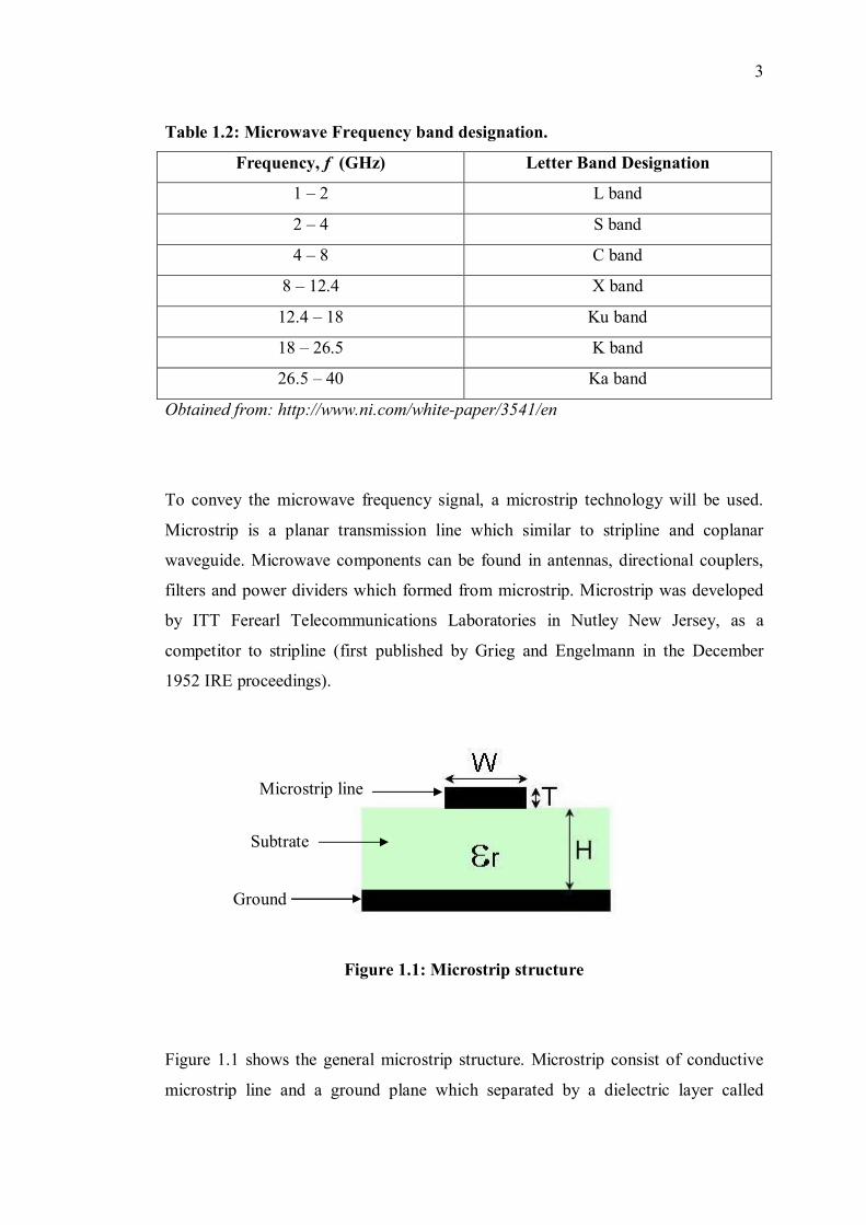
Table 1.2: Microwave Frequency band designation.
Frequency, f (GHz) Letter Band Designation
1 – 2 L band
2 – 4 S band
4 – 8 C band
8 – 12.4 X band
12.4 – 18 Ku band
18 – 26.5 K band
26.5 – 40 Ka band
Obtained from: http://www.ni.com/white-paper/3541/en
To convey the microwave frequency signal, a microstrip technology will be used.
Microstrip is a planar transmission line which similar to stripline and coplanar
waveguide. Microwave components can be found in antennas, directional couplers,
filters and power dividers which formed from microstrip. Microstrip was developed
by ITT Ferearl Telecommunications Laboratories in Nutley New Jersey, as a
competitor to stripline (first published by Grieg and Engelmann in the December
1952 IRE proceedings).
Figure 1.1: Microstrip structure
Figure 1.1 shows the general microstrip structure. Microstrip consist of conductive
microstrip line and a ground plane which separated by a dielectric layer called
Microstrip line
Subtrate
Ground

4
substrate. To design a microstrip, width (W) and thickness (T) of conductive
microstrip line and height (H) of the substrate are very important. Ԑr represent the
dielectric constant or relative permittivity of the substrate. In this project we will use
microstrip technology because all active components can be mounting on the top of
the board. Apart from microstrip are much less expensive, lighter and more compact.
In theoretical, effective dielectric constant (Ԑeff) and characteristics impedance (Zo) of
the microstrip line will be introduced. To find effective dielectric constant, below
equation can be use.
By using dimension of microstrip line H/W, characteristic impedance can calculated
as
By given the characteristic impedance and dielectric constant, dimension can be
calculated by below equation
Where

5
1.2 Aims and Objectives
Main objective of this project is to design a new microstrip directional coupler
technique which is patch-coupled directional coupler to achieve a wider bandwidth.
Author needs to understand fundamental theory of microstrip directional coupler
before start to implement the project. Author can get the related journals or articles
through IEEE Xplore database under the University Tunku Abdul Rahman (UTAR)
OPAC system. Besides that, author also can get information or knowledge from the
websites or Pozar book which provided in the library of UTAR.
The first proposed idea is to design a broadside-coupled patch directional coupler.
The designed directional coupler resonates between 2 to 7 GHz. This design is one of
the latest techniques of the microwave component. Coupler is a dual-mode
directional coupler which has wider bandwidth. Obviously, the more modes a
directional coupler has, the wider bandwidth is.
Throughout this project, author has gained better understanding and knowledge of
passive microwave components such as directional couplers, filters and power
dividers. Apart from that, author learned how to use the HFSS software to design
directional coupler. Authors can also using freelance software to compare the result
of simulation and experimental results. In the experiment, when students facing any
problem, students must try to solve the problem so that can get nearest or better
result compare to simulation result.

6
1.3 Project Motivation
Motivation of this project is to design a new microstrip directional coupler. After this
project, students understand the background and function of directional coupler. So
in the future, student can design more microwave components depending on the
needed of industry. In this experiment, students are going to design a microstrip
directional coupler that has wider bandwidth and higher performance.

7
CHAPTER 2
2 LITERATURE REVIEW
2.1 Background
Firstly, directional coupler will be introduced in this chapter. After that, a new design
methodology will also introduce which was published in IEEE Xplore database. The
design will be simulate and discuss by author. Lastly, simulation tools that have been
used in this project will be introduced such as High Frequency Structure Simulator
(HFSS), Microwave Office and Freelance Graphics software.
2.2 Directional Coupler
Directional couplers are passive reciprocal networks. It is a four-port network where
all four ports are ideally matched and lossless. Directional couplers can be realized in
microstrip, stripline, coax and waveguide. Directional couplers are used to sample a
signal, incident and reflected waves. Generally, couplers use distributed properties of
microwave circuits which coupling feature is a quarter or multiple quarter-
wavelengths. Purposes of directional couplers are used in RF (radio frequency) and
microwave routing for isolation, separating and combining signals.
Applications of directional coupler are providing a signal sample for measurement or
monitor, feedback, combining feeds to and from antenna. Directional coupler also
providing taps for cable distributed system such as cable television, separating

8
transmitted and received signals on telephone lines. Figure 2.1 shows an ideal
directional coupler schematic where port 1 is the input port, port 2 is through port,
port 3 is coupled port and port 4 is isolation port. The wave incident in port 1 couples
power into ports 2 and 3 but not into port 4.
Figure 2.1: Ideal Directional Coupler
Directional coupler has three specifications which is coupling (C), directivity (D) and
isolation (I). Coupling is ratio of input power to coupler power. Directivity is ratio of
coupled power to the power at isolated port. Isolation is ratio of input power to
power flow out of the isolated port. Isolation is also known as the sum of coupling
factor and directivity of directional coupler.
3
1log10PPC (dB)
4
3log10PPD (dB)
4
3
3
1
4
3
3
1
4
1 log10log10log10log10PP
PP
PP
PP
PPI (dB)
DCI (dB)
For a four-port network, S-matrix of a reciprocal and matched network has the
following form:
Isolation Port
Through Port
Input Port
Coupled Port
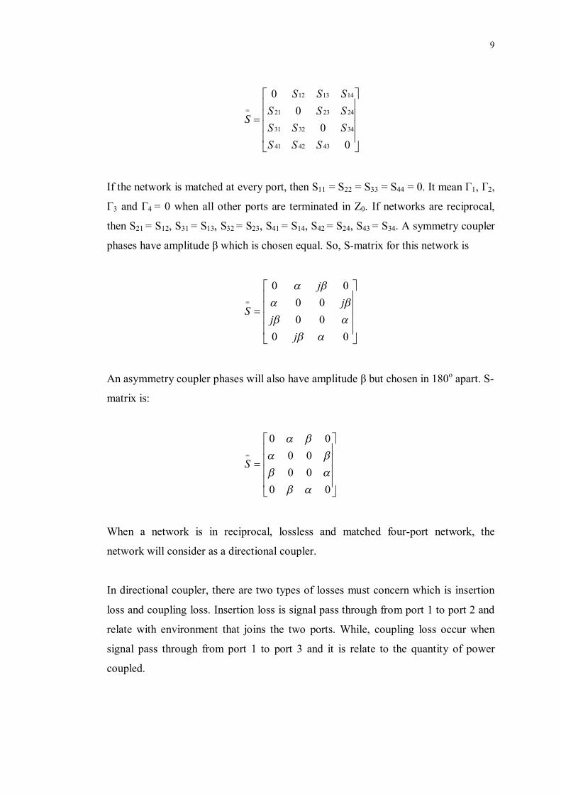
9
00
00
434241
343231
242321
141312
SSSSSSSSSSSS
S
If the network is matched at every port, then S11 = S22 = S33 = S44 = 0. It mean Γ1, Γ2,
Γ3 and Γ4 = 0 when all other ports are terminated in Z0. If networks are reciprocal,
then S21 = S12, S31 = S13, S32 = S23, S41 = S14, S42 = S24, S43 = S34. A symmetry coupler
phases have amplitude β which is chosen equal. So, S-matrix for this network is
000000
00
jj
jj
S
An asymmetry coupler phases will also have amplitude β but chosen in 180o apart. S-
matrix is:
000000
00
S
When a network is in reciprocal, lossless and matched four-port network, the
network will consider as a directional coupler.
In directional coupler, there are two types of losses must concern which is insertion
loss and coupling loss. Insertion loss is signal pass through from port 1 to port 2 and
relate with environment that joins the two ports. While, coupling loss occur when
signal pass through from port 1 to port 3 and it is relate to the quantity of power
coupled.

10
2.2.1 Conventional Coupled-line Directional Coupler
Conventional coupled-line directional coupler is one of the common methods to
design directional coupler. Figure 2.2 shows the conventional coupled-line
directional coupler structure.
Port 1
Port 2 Port 3
Port 4
Electrical lengthV1
V2 V3
V4
Z0
Z0
Z0
Z0
Figure 2.2: Conventional coupled-line directional coupler structure
In this structure, coupling level between the ports is due to interaction of
electromagnetic fields along transmission lines which have been placed in close
proximity. In additions, it can be named as TEM-mode quarter-wavelength
directional coupler. (Leo Young, M.A., Dr. Eng., 1963).
One method to analyze multi-port transmission line circuits such as coupled line is
through even and odd mode analysis. In this case, circuit input voltage is split into
two, even (symmetric) and odd (anti-symmetric) mode. Zoe is the characteristic
impedance of a transmission lines under even mode operation and Zoo is
characteristic impedance lines under the odd mode excitation.
Midband amplitude coupling factor, c is given in terms of even mode characteristics
impedance, eZ0 and odd mode characteristic impedance, oZ0 such as:
oe
oe
ZZZZc
00
00

11
Characteristic impedance 0Z is express in terms as:
oeZZZ 000
According to all the equations above, even and odd mode impedances can be writen
as :
ccZZ e
11
00
and
ccZZ o
11
00
With above equation, we can determine the width and separation of lines for given
coupling coefficient. Figure 2.3 shows even- and odd-mode characteristic impedance
that has been tabulated by Pozar, with a complete solution for the microstrip lines.
But only for r = 10. (David M. Pozar, 1998). Parameters used in the graph are
represented as below:
S = Separation
W = Width of Microstrip lines
D = Dielectric thickness

12
Figure 2.3: Even- and odd-mode characteristic impedance of coupled-line
directional coupler
2.2.2 Hybrid Coupler
Directional coupler can be made in many different forms such as waveguide coupler,
hybrid coupler, coupled transmission line form and etc. Hybrid coupler is a special
form in directional coupler which has coupling factor at 3dB and the phase between
ports can be either 90o or 180o which called quadratic hybrid and magic-T (rat-race)
hybrid.
Quadrature hybrid is a 3dB directional coupler with 90o phase difference in outputs
of the through and coupled arms. (David M. Pozar, 2005). Figure 2.4 shows
quadrature hybrid structure and also called branch-line coupler. Because all ports are
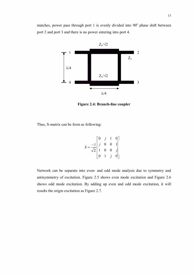
13
matches, power pass through port 1 is evenly divided into 90o phase shift between
port 2 and port 3 and there is no power entering into port 4.
Figure 2.4: Branch-line coupler
Thus, S-matrix can be form as following:
010001
100010
21
jj
jj
S
Network can be separate into even- and odd mode analysis due to symmetry and
antisymmetry of excitation. Figure 2.5 shows even mode excitation and Figure 2.6
shows odd mode excitation. By adding up even and odd mode excitation, it will
results the origin excitation as Figure 2.7.
Zo
λ/4
1
4
2
3
λ/4
Zo/√2
Zo/√2

14
Figure 2.5: Even mode excitation

15
Figure 2.6: Odd mode excitation
Figure 2.7: Branch-line circuit in normalized form
For even mode analysis, because voltages and currents are in the same above and
below the line of symmetry (LOS), so current will be equal zero at LOS. It is an open
circuit loads at the ends of the stub. While for odd mode analysis, voltages and
currents are opposite values above and below the LOS, it result the voltage equal to
zero along LOS which is short circuit loads at the ends of stub.
Since these two ports amplitude of incidents wave is ±1/2, then the amplitude of
emerging wave for each port can be sum up and expressed as following:

16
Where Γe,o and Te,o represents even and odd mode reflection and transmission
coefficient for two networks. By using ABCD matrices, Γe and Te, even mode of two
port circuit can be calculated by following:
Admittance of the shunt open-circuited stub is Y = jtanβl. Thus,
It is similarly to obtain odd mode reflection and transmission coefficient.
Odd mode reflection and transmission obtain as below:

17
Then Γe,o and Te,o substitute into amplitude of emerging wave for each port and
results:
B1 = 0
B2 =
B3 =
B4 = 0
From the results, when port 1 is excited and all other ports terminated in the matched
loads, then port 1 is matched (B1 = 0) and it is -90o phase shift from port 1 to port 2,
some more one half of the input power is delivered to port 2. Apart from that, there
are a 90o phase shift between port 3 and port 2 and one half of the input power is
delivered to port 3. At last, port 4 is no power out (B4 = 0).
.
2.3 Dual-band Filter with Stepped-impedance Resonators
In this sub-chapter, authors will introduce a design of microstrip that has published in
IEEE Electronics Letter by H.-J.Yuan and Y.Fan entitled “Compact microstrip dual-
band filter with stepped-impedance resonators”. Dual-band filter has become an
important device in communication systems because of the increasing demand for
wireless communications and the wireless LAN are widely used.
Figure 2.8 shows geometry and dimensions of the filter. Filter substrate with size of
52.2 mm and 40 mm, thickness of 1 mm, and relative permittivity of 9.2. This filter
consists of a stepped-impedance resonator and the quarter-wavelength impedance
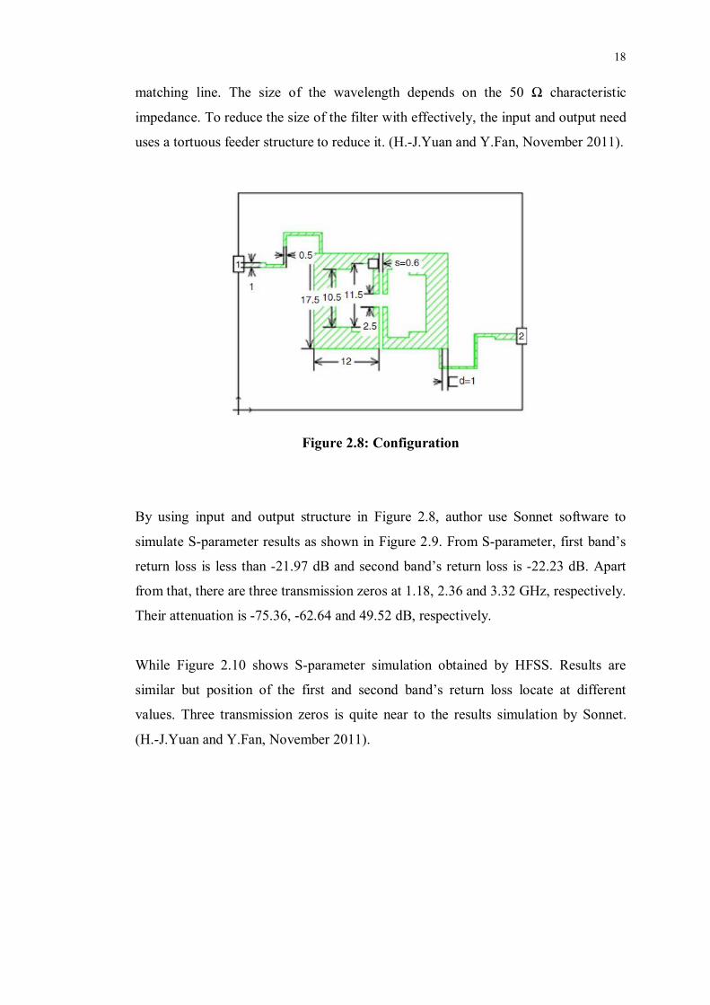
18
matching line. The size of the wavelength depends on the 50 Ω characteristic
impedance. To reduce the size of the filter with effectively, the input and output need
uses a tortuous feeder structure to reduce it. (H.-J.Yuan and Y.Fan, November 2011).
Figure 2.8: Configuration
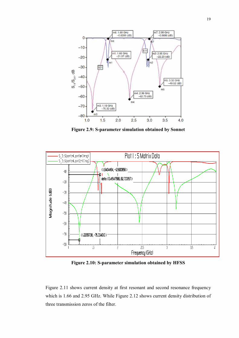
By using input and output structure in Figure 2.8, author use Sonnet software to
simulate S-parameter results as shown in Figure 2.9. From S-parameter, first band’s
return loss is less than -21.97 dB and second band’s return loss is -22.23 dB. Apart
from that, there are three transmission zeros at 1.18, 2.36 and 3.32 GHz, respectively.
Their attenuation is -75.36, -62.64 and 49.52 dB, respectively.
While Figure 2.10 shows S-parameter simulation obtained by HFSS. Results are
similar but position of the first and second band’s return loss locate at different
values. Three transmission zeros is quite near to the results simulation by Sonnet.
(H.-J.Yuan and Y.Fan, November 2011).
19
Figure 2.9: S-parameter simulation obtained by Sonnet
Figure 2.10: S-parameter simulation obtained by HFSS
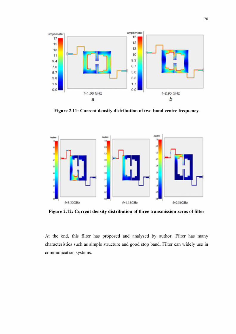
Figure 2.11 shows current density at first resonant and second resonance frequency
which is 1.66 and 2.95 GHz. While Figure 2.12 shows current density distribution of
three transmission zeros of the filter.
20
Figure 2.11: Current density distribution of two-band centre frequency
Figure 2.12: Current density distribution of three transmission zeros of filter
At the end, this filter has proposed and analysed by author. Filter has many
characteristics such as simple structure and good stop band. Filter can widely use in
communication systems.

21
2.4 Wideband Rectangular-shaped Directional coupler
This design presents of three-section rectangular-shaped directional coupler. Paper
can be found on IEEE Xplore database entitle “Design and Cross-Section Analysis of
Wideband Rectangular-Shaped Directional Coupler” by authors S.N.A.M. Ghazali,
N.Seman, R.C.Yob, M.K.A.Rahim and S.K.A.Rahim. This design offers a tight
coupling of 3dB over the designated frequency band of 2 to 6 GHz.
Proposed coupler consists of two substrates and one common ground plane between
the two substrates. Design was formed by rectangular-shaped microstrip line at the
top and bottom with rectangular slot at the common ground plane. The overall
dimension excluding microstrip ports occupy an area of 50 mm x 20 mm. In this
design, they are using CST Microwave Studio simulator to optimize the coupler.
The cross-section analysis was performed in order to study the characteristic of
electric field during the odd and even-mode excitation of the coupler. Figure 2.13
shows the overall view of the coupler configuration that shows two substrates are
sandwiched by the three conductor layers of top and bottom microstrip patch and one
layer of conductive coating in the middle which is the ground plane. While figure
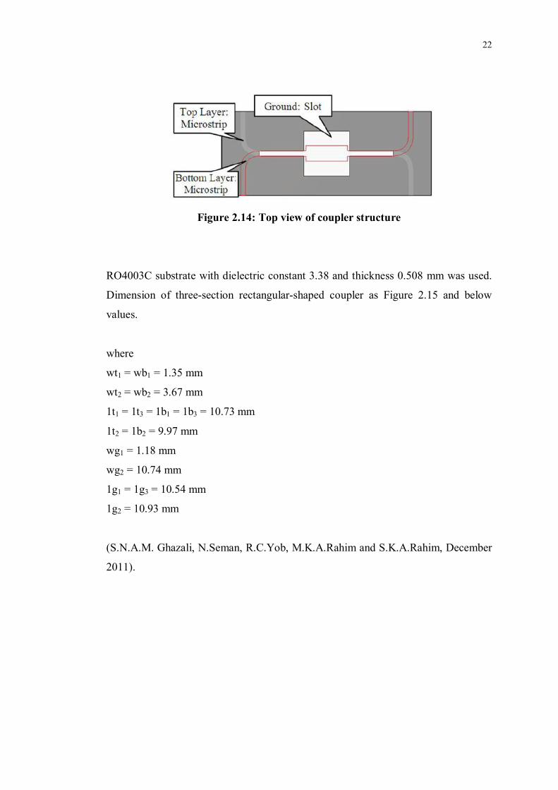
2.14 shows the top view of the coupler. (S.N.A.M. Ghazali, N.Seman, R.C.Yob,
M.K.A.Rahim and S.K.A.Rahim, December 2011).
Figure 2.13: Overall view of coupler configuration
22
Figure 2.14: Top view of coupler structure
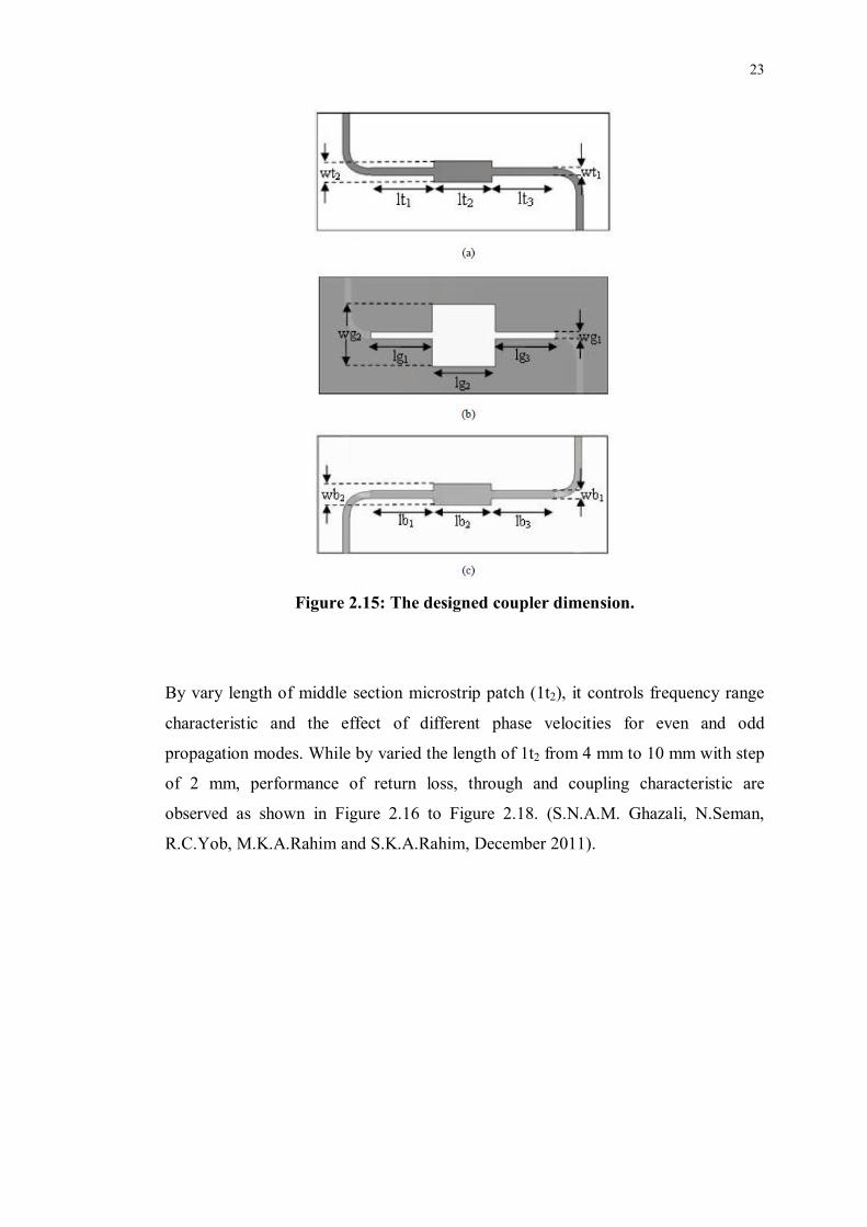
RO4003C substrate with dielectric constant 3.38 and thickness 0.508 mm was used.
Dimension of three-section rectangular-shaped coupler as Figure 2.15 and below
values.
where
wt1 = wb1 = 1.35 mm
wt2 = wb2 = 3.67 mm
1t1 = 1t3 = 1b1 = 1b3 = 10.73 mm
1t2 = 1b2 = 9.97 mm
wg1 = 1.18 mm
wg2 = 10.74 mm
1g1 = 1g3 = 10.54 mm
1g2 = 10.93 mm
(S.N.A.M. Ghazali, N.Seman, R.C.Yob, M.K.A.Rahim and S.K.A.Rahim, December
2011).
23
Figure 2.15: The designed coupler dimension.
By vary length of middle section microstrip patch (1t2), it controls frequency range
characteristic and the effect of different phase velocities for even and odd
propagation modes. While by varied the length of 1t2 from 4 mm to 10 mm with step
of 2 mm, performance of return loss, through and coupling characteristic are
observed as shown in Figure 2.16 to Figure 2.18. (S.N.A.M. Ghazali, N.Seman,
R.C.Yob, M.K.A.Rahim and S.K.A.Rahim, December 2011).
24
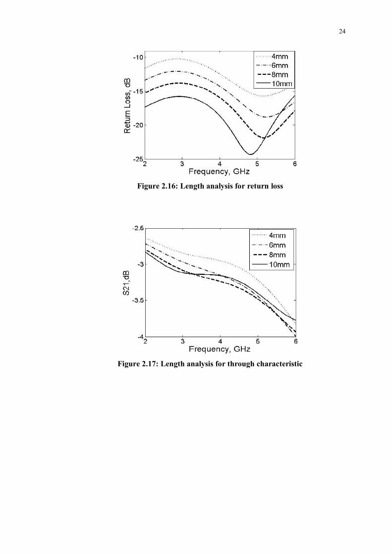
Figure 2.16: Length analysis for return loss
Figure 2.17: Length analysis for through characteristic
25
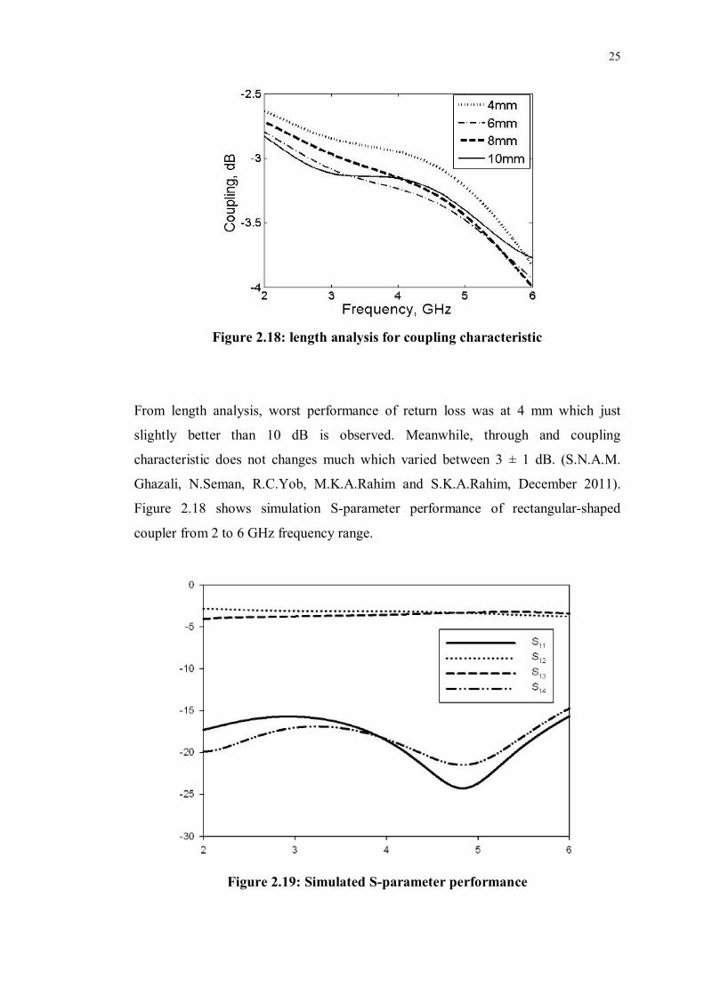
Figure 2.18: length analysis for coupling characteristic
From length analysis, worst performance of return loss was at 4 mm which just
slightly better than 10 dB is observed. Meanwhile, through and coupling
characteristic does not changes much which varied between 3 ± 1 dB. (S.N.A.M.
Ghazali, N.Seman, R.C.Yob, M.K.A.Rahim and S.K.A.Rahim, December 2011).
Figure 2.18 shows simulation S-parameter performance of rectangular-shaped
coupler from 2 to 6 GHz frequency range.
Figure 2.19: Simulated S-parameter performance
26
This coupler shows simulated return losses at all of its port and isolation between
port 1 and 4, and 2 and 3 are better than 15 dB from 2 to 6 GHz. In frequency range,
coupling coefficient between ports 1 and 3, and 2 and 4 is 3 dB ± 1 deviation. At the
end, its return loss and isolation have been confirmed for 2 to 6 GHz frequency range.
2.5 Dual-mode Bandpass Filter Using Slot Resonator
Microstrip filters with dual-mode property has been widely used in the design of
planar microwave filters. Therefore, a dual-mode bandpass filter by using a slot-line
square loop resonator is proposed by Bian Wu, Wen Su, Shou-jia Sun and Chang-
Hong Liang.
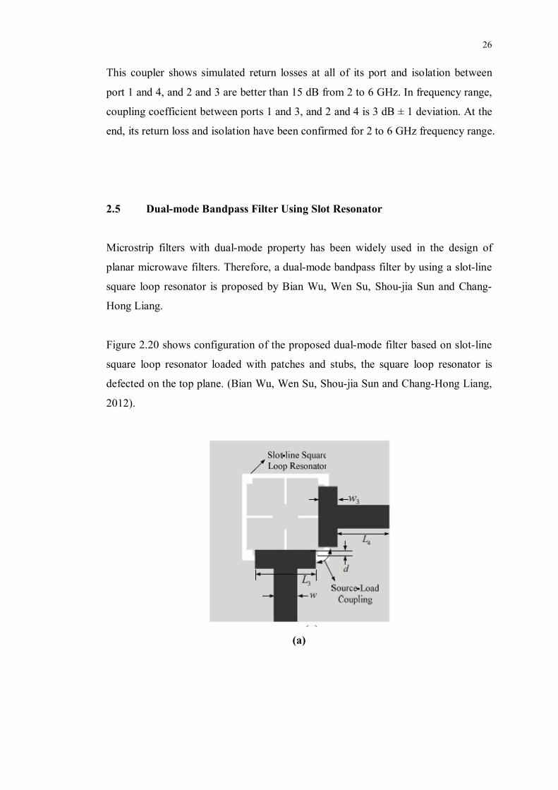
Figure 2.20 shows configuration of the proposed dual-mode filter based on slot-line
square loop resonator loaded with patches and stubs, the square loop resonator is
defected on the top plane. (Bian Wu, Wen Su, Shou-jia Sun and Chang-Hong Liang,
2012).
(a)

27
(b)
Figure 2.20: Proposed dual-mode filter configuration. (a) Total view, (b) Slot-
line square loop resonator (SSLR) loaded with patches and stubs.
A SSLR dual-mode filter with asymmetrical response is designed and fabricated as
shown in figure 2.21, the parameter are chosen as:
L1 = 10 mm
L2 = 3 mm
L3 = 7 mm
w1 = 0.5 mm
w2 = 0.2 mm
w3 = 2.2 mm
p = 0.65 mm
r = 0.7 mm
d = 0.7 mm
w = 2.7 mm

28
Figure 2.21: Prototype of the dual-mode SSLR filter
Simulation and experimental results are compared as shown in figure 2.22. From
figure 2.22, simulated center frequency is 3.55 GHz with a wide fractional bandwidth
of 3.7%. There are two transmission zeros appear at 4.09 GHz and 4.14 GHz, which
can improve the upper selectivity. From the results, experiments results agree well
with simulation except for a larger insertion loss of about 2.6 dB. It may due to
during fabrication error and radiation loss of the slot-line resonator. (Bian Wu, Wen
Su, Shou-jia Sun and Chang-Hong Liang, 2012).
Figure 2.22: S-parameter of the simulation and experiment
An asymmetrical wideband frequency response with two upper transmission zeros
are obtained by using the proposed SSLR and T-shaped feed lines. Dual-mode filter
has the advantages of relatively wideband and flexible transmission zeros to realize
either symmetrical or asymmetrical suppression. (Bian Wu, Wen Su, Shou-jia Sun
and Chang-Hong Liang, 2012).
29
2.6 Introduction of Simulation Tools
During this project, we are using a lot of tools for simulation and measurement to get
the proposed idea results such as High Frequency Structure Simulator (HFSS) and
Microwave Office. Besides that, we also need other tools such as TX Line for
calculate dimension of the strip line and Freelance Graphics software for plotting
graph for writing thesis purpose. In this sub-chapter, we will introduce HFSS and
Microwave office background.
2.6.1 High Frequency Structure Simulator
HFSS software is the industry-standard simulation tool for 3-D full-wave
electromagnetic field simulation and is essential for the design of high-frequency and
high-speed component design. HFSS offers multiple state-of the-art solver
technologies based on either the proven finite element method or the well established
integral equation method.
With the rapid advancement of HFSS, the analysis of the scattering matrix
parameters (S, Y, Z parameters) and the visualization of the 3-D electromagnetic
fields (near field and far field) can be done easily. It helps to determine the signal
quality, transmission path losses, and reflection coefficients due to impedance
mismatch, parasitic coupling, and radiation.
In conclusion, HFSS provides accurate results for diagnostics, prototyping and
manufacturing optimisation. The use of HFSS can speed up new product
development by orders of magnitude over conventional techniques. It also allows the
Engineer to play with unconventional designs.

30
2.6.2 Microwave Office
Microwave Office is RF and microwave design software for the industry's
microwave design platform with the fastest growing. Microwave Office has
revolutionized the communications design world by providing users with a superior
choice. Microwave Office offers unparalleled intuitiveness, powerful and innovative
technologies, and unprecedented openness and interoperability, enabling integration
tools for each part of the design process.
This software design suitable for high-frequency IC, PCB and module design
including linear circuit simulators, non-linear circuit simulators, electromagnetic
analysis tools, integrated schematic and layout, statistical design capabilities and
parametric cell libraries with built-in design-rule check (DRC). AWR is a very useful
tool which has a lot of pros such as faster time to market, efficiency, accurate for
high performance analysis,
31
CHAPTER 3
3 BROADSIDE-COUPLED PATCH DIRECTIONAL COUPLER
3.1 Background
In directional coupler design, there are three main stages. There are simulation,
fabrication and experiment stages. During these three stages, a lot of problem will
occur and time is needed to obtain a better results.
3.2 Simulation Stage
In simulation stage, we are using software called HFSS (High Frequency Structure
Simulator) which is in version 8. Before start design a new proposed idea, author
need go through the software tutorial. Tutorial purpose is allow users familiar with
the features and background of software.
After getting through HFSS tutorial, author go through few published paper and try
to get the similar result as the paper results. It allow author more confident on
simulation stages. Later on, few testing have been getting out for different directional
coupler design.
Firstly, author need simulate on different width and length of the design stripline to
match the 50Ω characteristic impedance. Width and length of the stripline can be
calculated by using TX Line 2003. After meet characteristic impedance, author
32
required a lot of time to optimize the correct parameter. At the end, a final
configuration and simulation result will be obtained.
3.3 Fabrication Stage
During this stage, author need show final simulation results to supervisor for
verifying. It is because author does not need to waste the board and time to redo the
design. Board material of this project is RO4003C substrate. This material has a 3.38
dielectric constant with 32 mil thickness. The board is called printed circuit board
(PCB).
PCB is used to support and electrically connect electronic components using
conductive pathways, track or signal traces etched from copper sheets laminated into
a non-conductive substrate. Conducting layers are typically made of thin copper foil.
Due to this material is not same as FR4 which they typically already laminated. So,
firstly, author need coat the board with a solder mask that is in blue colour. The
solder mask normally only available in green, black, white and red colour.
Next, author need transfer configuration printed on tracing paper to substrate. This is
a patter transfer process. During this process, author needs done the work in a clean
room which mean only yellow light are allowed. It is due to the photoresists are not
sensitive to wavelength which is greater than 0.5µm. Substrate only need exposed to
UV light for 15 seconds.
After that, PCB need for etching process. Purpose of this process is to remove the
unwanted copper and leaving only desired copper traces. After that a chemical
etching is done with ferric chloride in which the board is submerged in the etching
solution. This is simplest way for small-scale production, an immersion etching.
Fabrication process is considered done after completing this process.

33
3.4 Experiment Stage
This is last stages to design a new directional coupler. Before author start to measure
experimental results, author need to solder port with PCB. Purpose of this stage is for
author to compare simulation and experimental results. Due to comparison, author
can prove that the design can be worked in practically.
Equipment that used to measure experiment results is Rohde & Schwarz ZVB8
Vector Network Analyzer (VNA). Frequency range of this equipment is 300 kHz to
8 GHz. Equipment is design for high frequency device. In the first proposed design,
directional coupler has frequency range from 2GHz to 7GHz.
After solder port, author need calibrate on the VNA machine due to different cable
used has different phase of signal. VNA is able to self adjust on the S-parameters
after the calibration process. The main purpose of the calibration process is to
eliminate the effect of cable on the measurement and the results will more accurate.
Frequency range and sweep point have to be set in order to similar to simulation
result.
3.5 Broadside-coupled Patch Directional Coupler
In this subchapter, a broadside-coupled patch directional coupler was analyzing. This
is a four-port with two-mode directional coupler with wide bandwidth. With this
multi-port directional coupler, power splitting and network combining can be done
easily. (Ferdinando Alesssandri, Marco Giordano, Marco Guglielmi, Giacomo
Martirano, Francesco Vitulli, May 2003). Based on design theory that has discussed
on chapter 2, a four-port directional coupler with 10 dB fractional bandwidth is
simulated and discussed here.
34
3.5.1 Configuration
A directional coupler that operates with a center frequency of 5GHz was designed.
Substrate RO4003C with dielectric constant of r = 2.33 and thickness 32 mil was
used in this design. Apart from that, four-port of directional coupler are designed
with the characteristic impedance of 50 Ω. With the characteristic impedance of 50 Ω,
directional coupler designs can easily interconnecting with other microwave systems.
This broadside-coupled patch directional coupler is design by using two substrates
with the same dielectric constant and thickness. The overall dimensions of proposed
design occupy and area of 50 mm x 50 mm. Proposed design formed by a rectangular
and patch at the top and middle layer, where microstrip line is combining with the
patch at each layer. Input and through port was lay on the top layer of the substrate.
While coupler and isolation port was lay on the middle layer between two substrates.
Lastly, common ground plane was form on bottom of the substrate.
With the design requirements stated above, a directional coupler was drawn by using
Ansoft HFSS. Top-down view of the design is shown in figure below. Detailed
parameters are given by:
W1 = 14 mm
W2 = 31 mm
L1 = 5.6 mm
L2 = 3.3 mm
L3 = 3.4 mm
L4 = 3.1 mm
G1 = 3.4 mm
G2 = 4.0 mm
S1 = 50.0 mm
S2 = 50.0 mm

35
Figure 3.1: Dimension of broadside-coupled patch directional coupler
(a)
50Ω
50Ω

36
(b)
(c)
Figure 3.2: Prototype of the proposed broadside-coupled patch
directional coupler.
(a) Top-down view, (b) Side view, (c) Bottom view
3.5.2 Result and Discussion
In order to test performances of directional coupler design, experiments were carried
out by using Rohde and Schwarz ZVB8 VNA. Amplitude of the proposed directional
coupler was compared. Figure 3.3 shows magnitude response for the simulation and
experimental of broadside-coupled patch directional coupler.

37
Frequency (GHz)
2 3 4 5 6 7-60
-50
-40
-30
-20
-10
0
ExperimentHFSS
S11
S21S31
S41
|S(ij)| (dB)
Figure 3.3: Magnitude response of broadside-coupled patch directional coupler
Based on figure above, it is a two-mode directional coupler can be realised in the
proposed design. Experimental result was proven well with the simulation result.
From simulation and experimental result, a 10 dB flat coupling can be achieved in
frequency range of 4 to 5.5 GHz for simulation and 3.5 to 5.2 GHz for experimental
result. Simulation gives a total bandwidth of 1.5 GHz and experimental gives a total
bandwidth of 2 GHz.
Besides that, there are two poles contributing to wideband performance of the
directional coupler design. First pole locate at 3.6 GHz and second pole locate at 4.7
GHz for simulation result. While for experimental result, first pole locate at 3.5 GHz
and second pole at 5.1 GHz.
From Figure 3.3, center frequency and fractional bandwidth can be calculate and
form in Table 3.1 which shows comparison of the experimental and simulation
results. Equation center frequency, fractional bandwidth and difference between
simulation and experimental percentages as following:
38
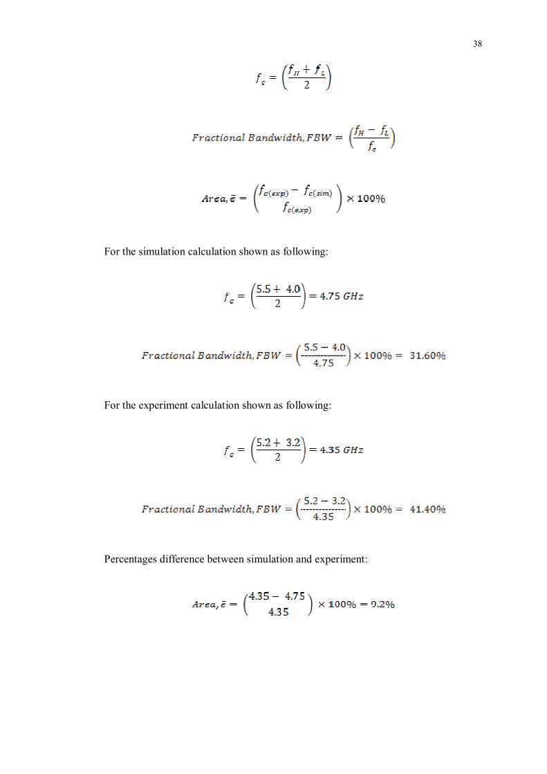
For the simulation calculation shown as following:
For the experiment calculation shown as following:
Percentages difference between simulation and experiment:
39
Table 3.1: Comparison of the experimental and simulation results
HFSS
Simulation
Experiment
fL (GHz), fH (GHz) 4.00, 5.50 3.20, 5.20
fc(GHz) 4.75 4.35
Fractional Bandwidth (%) 31.60 41.40
Fractional bandwidth difference between experimental and simulation is 9.2% which
is less than 10%. The difference between experimental and simulated may due to
alignment of two layers. That is very difficult to make exact alignment of two layer
same as alignment in the simulation part.
3.5.3 Parametric Analysis
In this subchapter, parametric analysis will be analyzed. We needs to simulate
proposed directional coupler using modified parameter with the same frequency
range in order to ease the comparison. It aims is to prove values selected in
configuration are able to perform better compare with other values. Different values
of design dimension are used to be simulated and results are discussed in this section.

40
Analysis 1
Parameter : W1
Optimum value : 14.0 mm
Step-down value : 13.8 mm
Step-up value : 14.2 mm
Result:
Frequency GHz2 3 4 5 6 7
-60
-50
-40
-30
-20
-10
0S21
S31
S41S11
|S(ij)| (dB)
W1 = 13.8 mmW1 = 14.0 mmW1 = 14.2 mm
Figure 3.4: Effect of width W1 on the proposed directional coupler
Parameter W1 does not affect simulation results much on the proposed directional
coupler. It only slightly affects the position poles on proposed directional coupler.
According to Figure 3.4, optimal value of W1 can give the best reflection coefficient
S11 with a matching level below -25 dB across the operating frequency band.
41
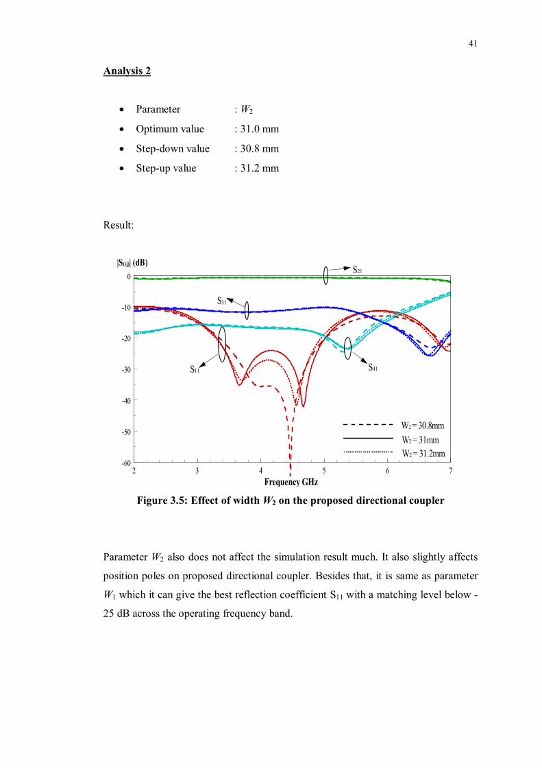
Analysis 2
Parameter : W2
Optimum value : 31.0 mm
Step-down value : 30.8 mm
Step-up value : 31.2 mm
Result:
2 3 4 5 6 7-60
-50
-40
-30
-20
-10
0
Frequency GHz
S21
S31
S11 S41
|S(ij)| (dB)
W2 = 30.8mmW2 = 31mmW2 = 31.2mm
Figure 3.5: Effect of width W2 on the proposed directional coupler
Parameter W2 also does not affect the simulation result much. It also slightly affects
position poles on proposed directional coupler. Besides that, it is same as parameter
W1 which it can give the best reflection coefficient S11 with a matching level below -
25 dB across the operating frequency band.

42
Analysis 3
Parameter : L1
Optimum value : 5.6 mm
Step-down value : 5.1 mm
Step-up value : 6.1 mm
Result:
2 3 4 5 6 7-60
-50
-40
-30
-20
-10
0
Frequency GHz
S41
S21
S31
S11
|S(ij)| (dB)
L1 = 5.1 mmL1 = 5.6 mmL1 = 6.1 mm
Figure 3.6: Effect of length L1 on the proposed directional coupler
When the length of center patch getting larger, the matching at port 1 will also
changes. Refer to Figure 3.6, matching level is maintained below -25 dB at optimum
gap of 5.60 mm. This is important to ensure that the input signal is not reflected back
to input port.

43
Analysis 4
Parameter : L2
Optimum value : 3.3 mm
Step-down value : 3.1 mm
Step-up value : 3.5 mm
Result:
2 3 4 5 6 7-60
-50
-40
-30
-20
-10
0
Frequency GHz
S11
S31
S41
S21|S(ij)| (dB)
L2 = 3.1 mmL2 = 3.3 mmL2 = 3.5 mm
Figure 3.7: Effect of length L2 on the proposed directional coupler
It is same as when the length of top patch larger and the matching at port 1 will also
change. But it does not affect the coupling port. When the length of top patch equal
to 3.5 mm, the matching at port 1 will become one-mode. It also does not affect the
other three ports.

44
Analysis 5
Parameter : L3
Optimum value : 3.1 mm
Step-down value : 2.9 mm
Step-up value : 3.3 mm
Result:
2 3 4 5 6 7-60
-50
-40
-30
-20
-10
0
S41
S21
S31
S11
|S(ij)| (dB)
Frequency GHz
L3 = 2.9 mmL3 = 3.1 mmL3 = 3.3 mm
Figure 3.8: Effect of length L3 on the proposed directional coupler
Length L3 has no significant effect on the coupling level. However, it causes the
matching to vary. Obviously, it is much better when L3 is equal to the optimum value.
It can be maintained well below -25 dB.

45
Analysis 6
Parameter : L4
Optimum value : 0.9 mm
Step-down value : 0.7 mm
Step-up value : 1.1 mm
Result:
2 3 4 5 6 7-60
-50
-40
-30
-20
-10
0
S41
S21
S31
S11
|S(ij)| (dB)
Frequency GHz
L4 = 0.7 mmL4 = 0.9 mmL4 = 1.1 mm
Figure 3.9: Effect of length L4 on the proposed directional coupler
The input of proposed directional coupler is affected when the length L4 changes.
When L4 is decreased, the first pole of the directional coupler shifts higher. Also, it
moves to combine with the second pole. The through port keep remain approximate
0 dB. That mean, most of the signal passed through the device and the return loss is
weak.

46
Analysis 7
Parameter : G1
Optimum value : 3.4 mm
Step-down value : 2.4 mm
Step-up value : 4.4 mm
Result:
2 3 4 5 6 7-60
-50
-40
-30
-20
-10
0
Frequency GHz
S21
S31
S11
S41
|S(ij)| (dB)
G1 = 2.4 mmG1 = 3.4 mmG1 = 4.4 mm
Figure 3.10: Effect of gap G1 on the proposed directional coupler
As for the coupled-line directional coupler, the gap between the top patch and middle
stripline play an important role in the determination of the desired coupling level of
the directional coupler. When the gap G1 is stepped down to 2.4 mm, the matching
level becomes poorer while the coupling level stays below 10 ± 1 dB. In another case,
G1 is stepped up to 4.4 mm, the coupling level is only about -14 1 dB, which is not
the desired value. The optimum gap size for G1 is 3.4 mm.
47
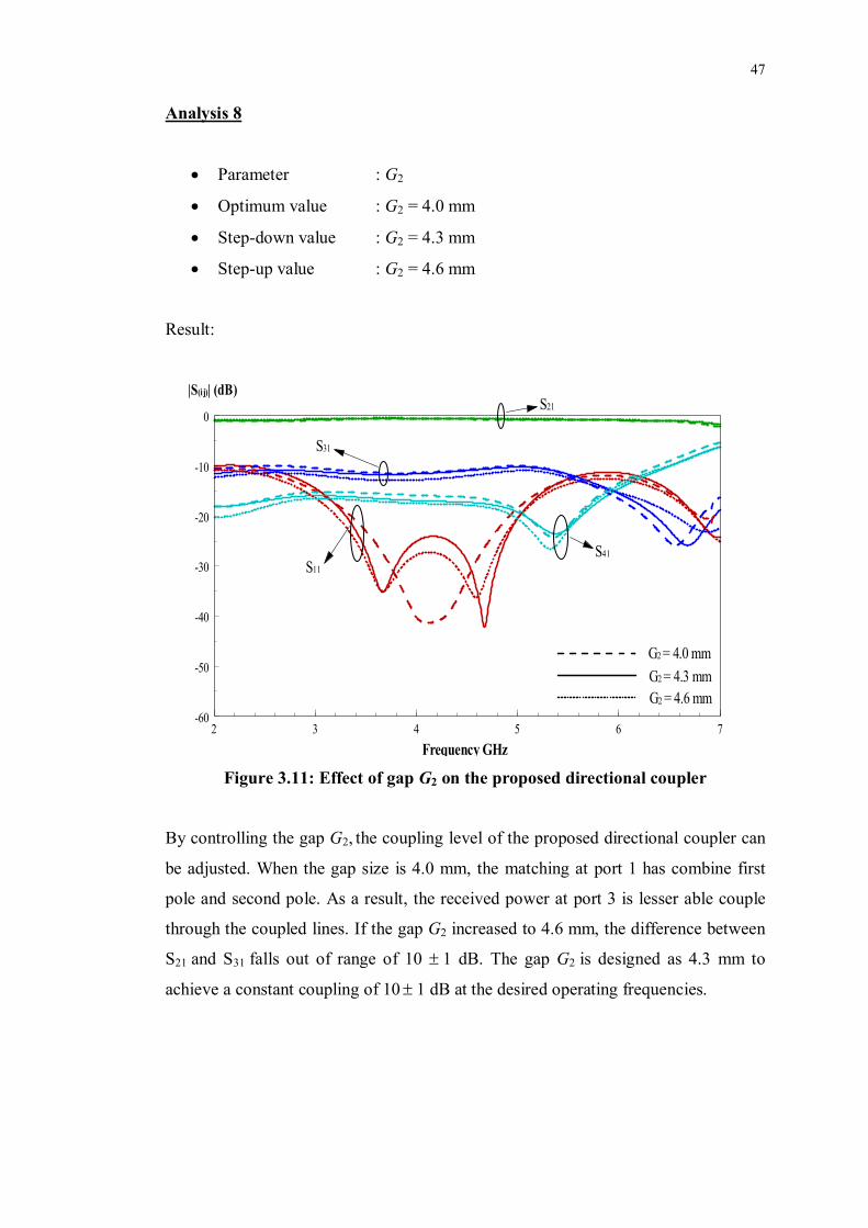
Analysis 8
Parameter : G2
Optimum value : G2 = 4.0 mm
Step-down value : G2 = 4.3 mm
Step-up value : G2 = 4.6 mm
Result:
Frequency GHz2 3 4 5 6 7
-60
-50
-40
-30
-20
-10
0S21
S31
S41S11
|S(ij)| (dB)
G2 = 4.0 mmG2 = 4.3 mmG2 = 4.6 mm
Figure 3.11: Effect of gap G2 on the proposed directional coupler
By controlling the gap G2, the coupling level of the proposed directional coupler can
be adjusted. When the gap size is 4.0 mm, the matching at port 1 has combine first
pole and second pole. As a result, the received power at port 3 is lesser able couple
through the coupled lines. If the gap G2 increased to 4.6 mm, the difference between
S21 and S31 falls out of range of 10 1 dB. The gap G2 is designed as 4.3 mm to
achieve a constant coupling of 10 1 dB at the desired operating frequencies.

48
Analysis 9
Parameter : S1
Optimum value : 50 mm
Step-down value : 40 mm
Step-up value : 60 mm
Result:
Frequency GHz2 3 4 5 6 7
-60
-50
-40
-30
-20
-10
0 S21
S31
S41
S11
|S(ij)| (dB)
S1 = 40 mmS1 = 50 mmS1 = 60 mm
Figure 3.12: Effect of substrate S1 on the proposed directional coupler
When the substrate length is not optimum value, the matching port was totally
changed and the return loss was so high. Apart from that, the bandwidth of coupling
port was less than 10 ±1 dB. It may due to the stripline of two layers become shorter,
the impedance matching was reduced.

49
Analysis 10
Parameter : S2
Optimum value : 50 mm
Step-down value : 40 mm
Step-up value : 60 mm
Result:
Frequency GHz2 3 4 5 6 7
-60
-50
-40
-30
-20
-10
0S21
S31
S41S11
|S(ij)| (dB)
S2 = 40 mmS2 = 50 mmS2 = 60 mm
Figure 3.13: Effect of substrate S2 on the proposed directional coupler
The coupling level was totally out of the range when S2 set to 40 mm. The fractional
bandwidth cannot maintain in the range of 10 ± 1 dB. Besides that, the position of
the two poles was shift to 3.1 GHz and 5.6 GHz. But when the S2 set to 60 mm, the
coupling level does not affect by the changes.
50
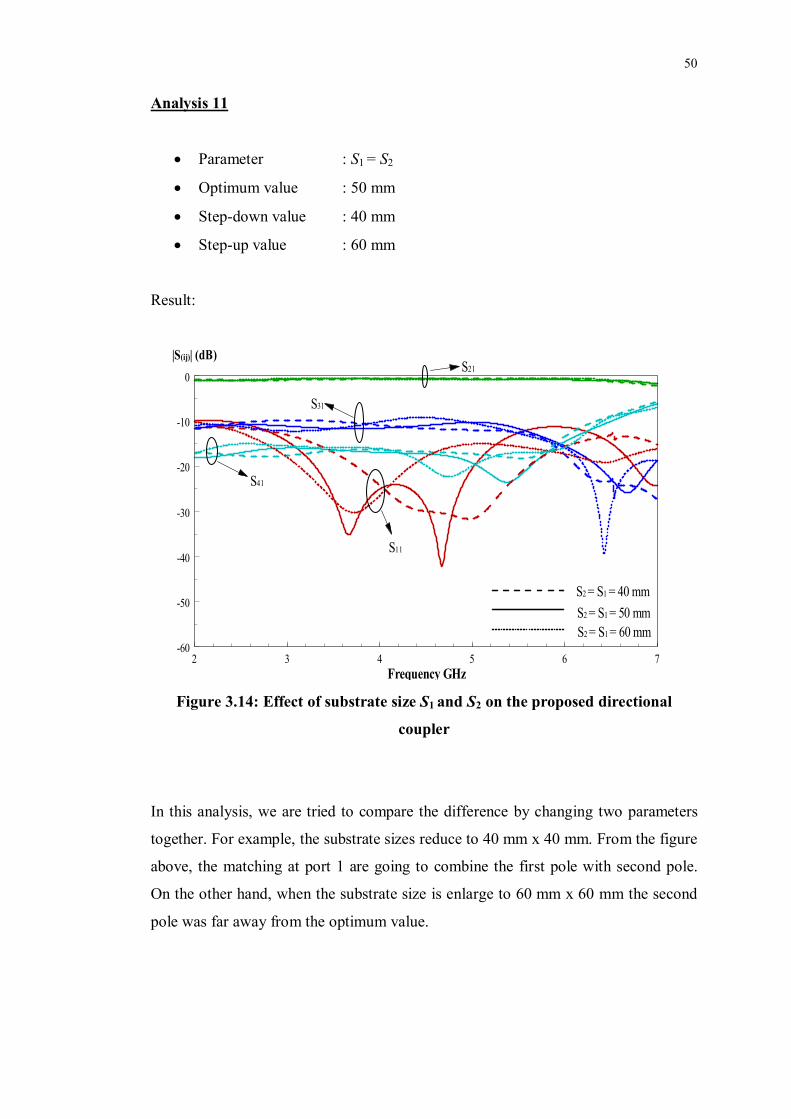
Analysis 11
Parameter : S1 = S2
Optimum value : 50 mm
Step-down value : 40 mm
Step-up value : 60 mm
Result:
2 3 4 5 6 7-60
-50
-40
-30
-20
-10
0S21
S31
S41
S11
Frequency GHz
|S(ij)| (dB)
S2 = S1 = 40 mmS2 = S1 = 50 mmS2 = S1 = 60 mm
Figure 3.14: Effect of substrate size S1 and S2 on the proposed directional
coupler
In this analysis, we are tried to compare the difference by changing two parameters
together. For example, the substrate sizes reduce to 40 mm x 40 mm. From the figure
above, the matching at port 1 are going to combine the first pole with second pole.
On the other hand, when the substrate size is enlarge to 60 mm x 60 mm the second
pole was far away from the optimum value.

51
Analysis 12
Parameter : H1
Optimum value : 0.8128 mm
Step-up value : 1.5240 mm
Result:
2 3 4 5 6 7-60
-50
-40
-30
-20
-10
0 S21
S31
S41S11
Frequency GHz
|S(ij)| (dB)
H1 = 1.5240 mm
H1 = 0.8128 mm
Figure 3.15: Effect of substrate thickness H1 on the proposed directional coupler
In this analysis, we are using the same dielectric constant with different thickness.
The substrate that we compare is a RO4003C with thickness 32 mil and 60 mil which
is 0.8128 mm and 1.5240 mm. It is better if the matching at port 1 was less than -10
dB. By using the 60 mil thickness, the coupling level was higher than 10 ± 1 dB. So
the optimum value is chosen to be 0.8128.

52
Analysis 13
Parameter : L2 , L3
Optimum value : L2 = 3.3 mm, L3 = 3.1 mm
Step-down value : L2 = L3 = 2.8 mm
Step-up value : L2 = L3 = 3.8 mm
Result:
2 3 4 5 6 7-60
-50
-40
-30
-20
-10
0 S21
S31
S41S11
|S(ij)| (dB)
Frequency GHz
L2 = L3 = 2.8 mmL2 = 3.3 mmL3 = 3.1 mmL2 = L3 = 3.8 mm
Figure 3.16: Effect of length L2 and L3 on the proposed directional coupler
With reference to the amplitude response shown in Figure 3.16, we can clearly see
that the gap g2 affects the input port of the proposed directional coupler. When L2
and L3 are set as 2.8 mm, the poles were difference with the optimum choice. When
L2 and L3 are stepped up to 3.8 mm, the matching level was not maintained at the
25dB. In this case, the value of L2 and L3 is chosen to be 3.3 mm and 3.1 mm.

53
Analysis 14
Parameter : L1 , L4
Optimum value : L1 = 5.6 mm, L4 = 0.9 mm
Step-down value : L1 = L4 = 5.2 mm
Step-up value : L1 = L4 = 6.0 mm
Result:
Frequency GHz
|S(ij)| (dB)
2 3 4 5 6 7-60
-50
-40
-30
-20
-10
0S21
S31S41
S11
L1 = L4 = 5.2 mmL1 = 5.6 mmL4 = 0.9 mmL1 = L4 = 6.0 mm
Figure 3.17: Effect of length L1 and L4 on the proposed directional coupler
When the length of the middle and top patch are equal, the characteristic impedance
of the top patch is no longer 50Ω. So, most of the signal cannot pass through the
device and the coupling level cannot maintain on 10 ± 1 dB. There is a high return
loss and low insertion loss.
54
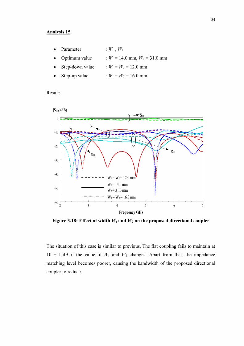
Analysis 15
Parameter : W1 , W2
Optimum value : W1 = 14.0 mm, W2 = 31.0 mm
Step-down value : W1 = W2 = 12.0 mm
Step-up value : W1 = W2 = 16.0 mm
Result:
Frequency GHz2 3 4 5 6 7
-60
-50
-40
-30
-20
-10
0S21
S31
S41S11
|S(ij)| (dB)
W1 = W2 = 12.0 mmW1 = 14.0 mmW2 = 31.0 mmW1 = W2 = 16.0 mm
Figure 3.18: Effect of width W1 and W2 on the proposed directional coupler
The situation of this case is similar to previous. The flat coupling fails to maintain at
10 1 dB if the value of W1 and W2 changes. Apart from that, the impedance
matching level becomes poorer, causing the bandwidth of the proposed directional
coupler to reduce.

55
Analysis 16
Parameter : G1 , G2
Optimum value : G1 = 3.4 mm, G2 = 4.3 mm
Step-down value : G1 = 2.4 mm, G2 = 3.3 mm
Step-up value : G1 = 4.4 mm, G2 = 5.3 mm
Result:
Frequency GHz2 3 4 5 6 7
-60
-50
-40
-30
-20
-10
0 S21
S31
S41S11
|S(ij)| (dB)
G1 = 2.4 mm, G2 = 3.3 mmG1 = 3.4 mmG2 = 4.3 mmG1 = 4.4 mm, G2 = 5.3 mm
Figure 3.19: Effect of gap G1 and G2 on the proposed directional coupler
Figure 3.19 shows the effect of G1 and G2 on the magnitude response. It can be seen
that flat coupling fails to maintain at 10 1 dB if the value of G1 and G2 changes.
Apart from that, the first pole was combining together with second pole when the G1
and G2 set to 5.3 mm.
56
CHAPTER 4
4 TRAVELLING-WAVE SECTORIAL SLOT RESONATOR
4.1 Background
Microwave resonators are widely used in a variety of application, including filters,
oscillator, frequency meters and tuned amplifiers. Operations of microwave
resonators are very similar to lumped-element resonators of circuit theory. Various
implementations of resonators at microwave frequencies distributed elements such as
transmission lines, rectangular and circular waveguide, and dielectric cavities. In this
chapter, we will discuss proposed resonator which is a travelling-wave slot resonator.
A resonator is a device or system that exhibits resonance or resonant behaviour. It
naturally oscillates at resonant frequencies, with greater amplitude than at others. The
oscillations in a resonator can be either electromagnetic or mechanical. Resonators
are used to either generate waves of specific frequencies or to select specific
frequencies from a signal. A microwave resonator can usually either a series or
parallel RLC lumped-element equivalent circuit.
57
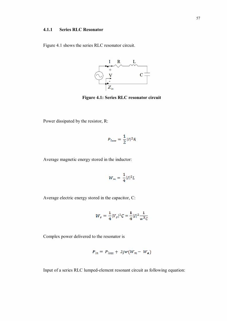
4.1.1 Series RLC Resonator
Figure 4.1 shows the series RLC resonator circuit.
Figure 4.1: Series RLC resonator circuit
Power dissipated by the resistor, R:
Average magnetic energy stored in the inductor:
Average electric energy stored in the capacitor, C:
Complex power delivered to the resonator is
Input of a series RLC lumped-element resonant circuit as following equation:
58
Quality factor and bandwidth:
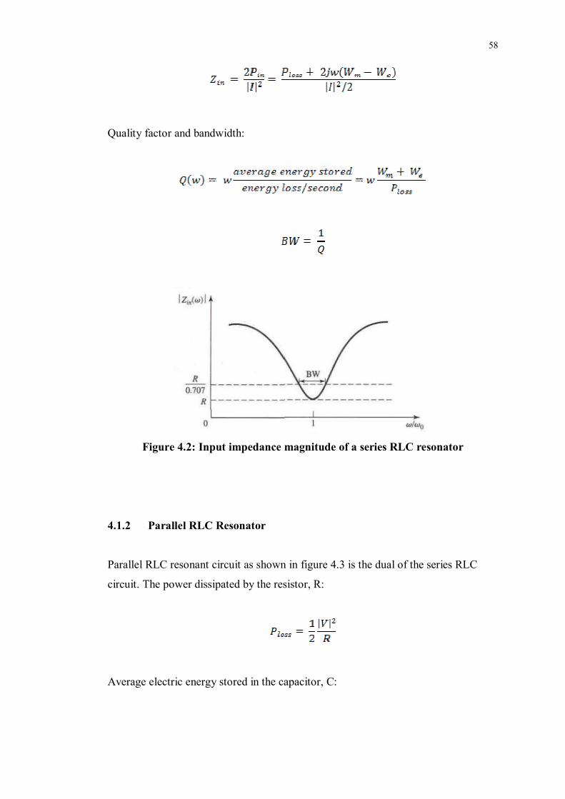
Figure 4.2: Input impedance magnitude of a series RLC resonator
4.1.2 Parallel RLC Resonator
Parallel RLC resonant circuit as shown in figure 4.3 is the dual of the series RLC
circuit. The power dissipated by the resistor, R:
Average electric energy stored in the capacitor, C:
59
Average magnetic energy stored in the inductor:
The IL is the current pass through the inductor. Then complex power delivered to the
resonator is
Similarly, the input of a series RLC lumped-element resonant circuit as following
equation:
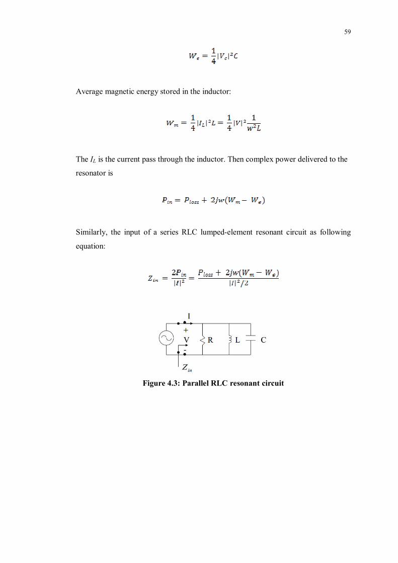
Figure 4.3: Parallel RLC resonant circuit

60
Figure 4.4: The input impedance magnitude of the parallel RLC resonator.
4.2 Configuration
Configuration travelling-wave sectorial slot resonator design shown as Figure 4.5. It
is a RO4003C substrate with thickness of 32 mil and dielectric constant of 3.38.
Design has two substrates with the same material. The first slot was laid on top layer
of the first substrate. The second slot lay on bottom layer of second substrate.
Dimension details of the configuration and results will be discussed in this
subchapter. The design is still under optimizing the exact parameters.
Figure 4.5 shows proposed resonator configuration which is still under optimizing.
The figure included bottom-layer, top-layer and middle-layer structure. From the
configuration, author can know that signals are pass by input port (port 1) to output
port (port 2 and port 3) through the slot in middle layer. Dimension of resonator as
following:
r = 3.38
H1 = 0.8128 mm / 32 mil
W1 = 1.75 mm
W2 = W3 = 1.7 mm
R1 = 14 mm
R2 = 12 mm
R3 = 8 mm
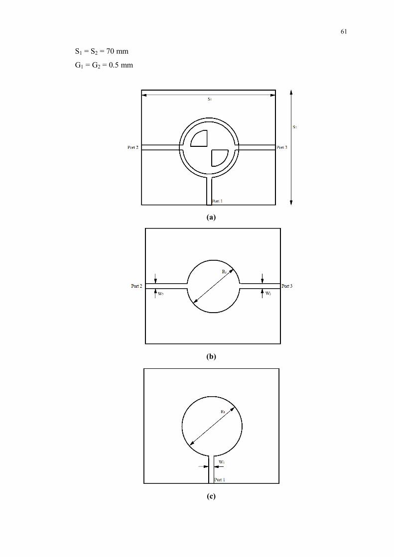
61
S1 = S2 = 70 mm
G1 = G2 = 0.5 mm
(a)
(b)
(c)

62
(d)
Figure 4.5: Configuration of the proposed resonator (a) Top-down view (b)
Bottom-layer structure (c) top-layer structure (d) middle-layer structure
4.3 Results and Discussion
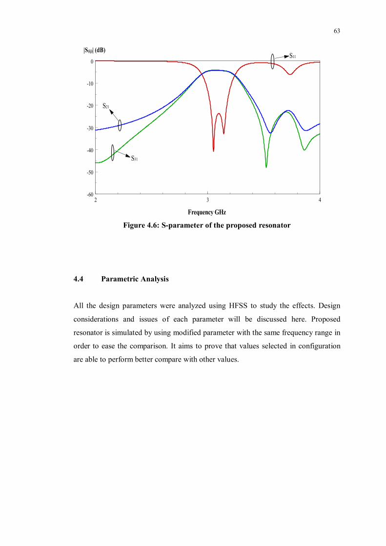
Figure 4.6 shows S-parameter of the proposed resonator. This S-parameter is a
reference for comparing the parameter analysis due to the design is still under
optimizing stages. The frequency should move to 3 GHz. It is because most of the
communication system is at 3 GHz.
From below figure, input impedance is lower than 12 dB which means signal pass
through the device is higher and the return loss is low. It is a two-mode resonator
which the poles are at 3.05 GHz and 3.14 GHz with center frequency at 3.1 GHz. For
this design, author cannot get experimental results due to run out of time. Another
problem is center frequency need move to 3 GHz.
63
2 3 4-60
-50
-40
-30
-20
-10
0
Frequency GHz
|S(ij)| (dB)
S21
S31
S11
Figure 4.6: S-parameter of the proposed resonator
4.4 Parametric Analysis
All the design parameters were analyzed using HFSS to study the effects. Design
considerations and issues of each parameter will be discussed here. Proposed
resonator is simulated by using modified parameter with the same frequency range in
order to ease the comparison. It aims to prove that values selected in configuration
are able to perform better compare with other values.
64
Analysis 1
Parameter : R1
Optimum value : R1 = 13 mm
Step-down value : R1 = 12 mm
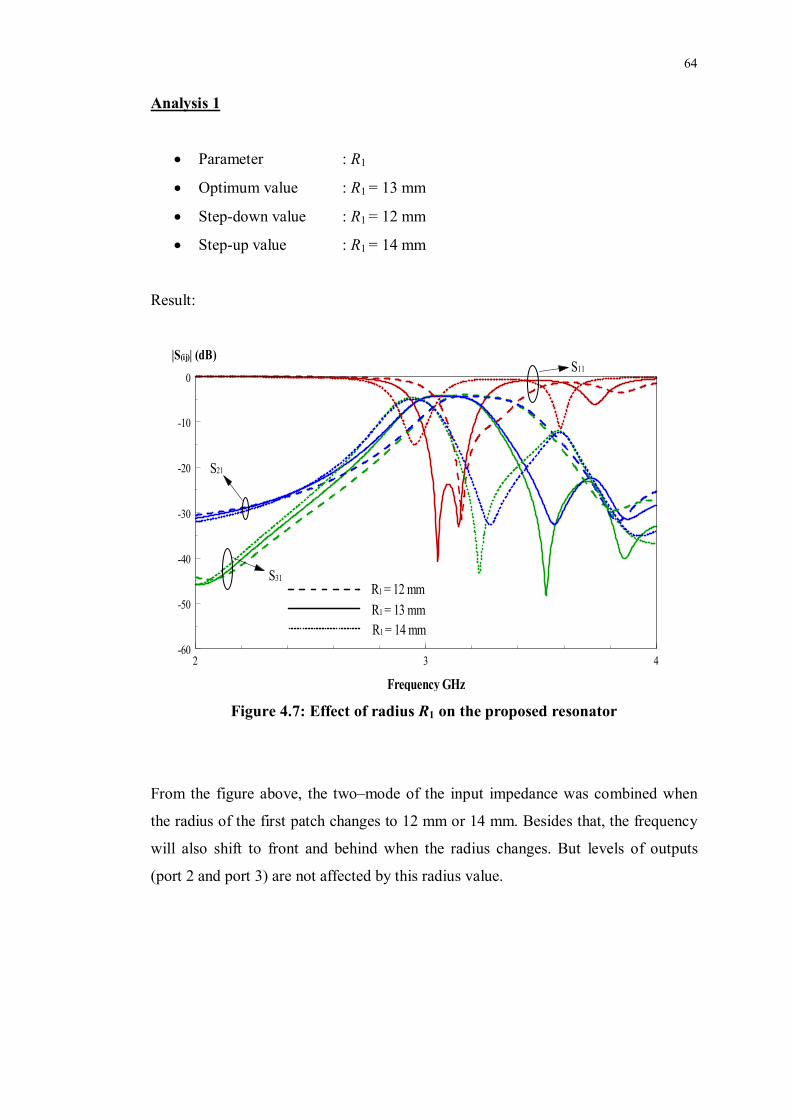
Step-up value : R1 = 14 mm
Result:
2 3 4-60
-50
-40
-30
-20
-10
0
S21
S31
S11
Frequency GHz
|S(ij)| (dB)
R1 = 12 mmR1 = 13 mmR1 = 14 mm
Figure 4.7: Effect of radius R1 on the proposed resonator
From the figure above, the two–mode of the input impedance was combined when
the radius of the first patch changes to 12 mm or 14 mm. Besides that, the frequency
will also shift to front and behind when the radius changes. But levels of outputs
(port 2 and port 3) are not affected by this radius value.

65
Analysis 2
Parameter : R2
Optimum value : R2 = 12 mm
Step-down value : R2 = 11 mm
Step-up value : R2 = 13 mm
Result:
2 3 4-60
-50
-40
-30
-20
-10
0
S21
S31
S11
Frequency GHz
|S(ij)| (dB)
R2 = 11 mmR2 = 12 mmR2 = 13 mm
Figure 4.8: Effect of radius R2 on the proposed resonator
When the radius of second patch changes, the two-modes of S11 was combine
together. But when the radius value step-up to 13 mm, the frequency is shift to 3
GHz which is we needed but it there is only one pole exists. The radius was chosen
to be optimum value 12 mm to maintain the two-mode input matching.

66
Analysis 3
Parameter : R3
Optimum value : R3 = 8 mm
Step-down value : R3 = 7 mm
Step-up value : R3 = 9 mm
Result:
2 3 4-60
-50
-40
-30
-20
-10
0
S21
S31
S11
Frequency GHz
|S(ij)| (dB)
R3 = 7 mmR3 = 8 mmR3 = 9 mm
Figure 4.9: Effect of radius R3 on the proposed resonator
From the figure 4.9, it shows that the results for input impedance was look very nice
when the radius of the middle slot was step-up to 9 mm. It has wider bandwidth and
the center requency at 3 GHz, but the input impedance level was higher than 12 dB.
On the other hand, the radius value step-down to 7 mm, the S11 was become badly.
So the optimum value of radius for the slot to be 8 mm.
67
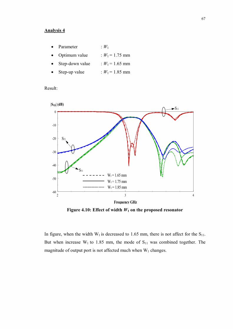
Analysis 4
Parameter : W1
Optimum value : W1 = 1.75 mm
Step-down value : W1 = 1.65 mm
Step-up value : W1 = 1.85 mm
Result:
2 3 4-60
-50
-40
-30
-20
-10
0
S21
S31
S11
Frequency GHz
|S(ij)| (dB)
W1 = 1.65 mmW1 = 1.75 mmW1 = 1.85 mm
Figure 4.10: Effect of width W1 on the proposed resonator
In figure, when the width W1 is decreased to 1.65 mm, there is not affect for the S11.
But when increase W1 to 1.85 mm, the mode of S11 was combined together. The
magnitude of output port is not affected much when W1 changes.

68
Analysis 5
Parameter : W2
Optimum value : W2 = 1.7 mm
Step-down value : W2 = 1.6 mm
Step-up value : W2 = 1.8 mm
Result:
2 3 4-60
-50
-40
-30
-20
-10
0
S21
S31
S11
Frequency GHz
|S(ij)| (dB)
W2 = 1.6 mmW2 = 1.7 mmW2 = 1.8 mm
Figure 4.11: Effect of width W2 on the proposed resonator
Parameter W2 does not bring much effect on the proposed resonator. It introduces
shift in the position of poles of the resonator when the width is altered. As can be
seen in Figure 4.11, the optimum value of W2 gives the best reflection coefficient S11.
Apart from that, it has no significant effect on output port.

69
Analysis 6
Parameter : W3
Optimum value : W3 = 1.7 mm
Step-down value : W3 = 1.6 mm
Step-up value : W3 = 1.8 mm
Result:
2 3 4-60
-50
-40
-30
-20
-10
0
S21
S31
S11
Frequency GHz
|S(ij)| (dB)
W3 = 1.6 mmW3 = 1.7 mmW3 = 1.8 mm
Figure 4.12: Effect of width W3 on the proposed resonator
The result of W3 is same as the results of W2. There are not many changes when the
width was changes. Just the mode of input port was combined together when the
width step-down to 1.6 mm.

70
Analysis 7
Parameter : S1
Optimum value : S1 = 70 mm
Step-down value : S1 = 50 mm
Step-up value : S1 = 80 mm
Result:
2 3 4-60
-50
-40
-30
-20
-10
0
S21
S31
S11
Frequency GHz
|S(ij)| (dB)
S1 = 50 mmS1 = 70 mmS1 = 80 mm
Figure 4.13: Effect of size S1 on the proposed resonator
The S1 does not affect the result much just the position of the poles was shift to left
when the size step-up to 80 mm. When size was step-down to 50 mm, two-poles was
combined together. This is not an important parameter if only changes this parameter.

71
Analysis 8
Parameter : S2
Optimum value : S2 = 70 mm
Step-down value : S2 = 50 mm
Step-up value : S2 = 80 mm
Result:
2 3 4-60
-50
-40
-30
-20
-10
0
S21
S31
S11
Frequency GHz
|S(ij)| (dB)
S2 = 50 mmS2 = 70 mmS2 = 80 mm
Figure 4.14: Effect of size S2 on the proposed resonator
Result for this parameter is same as S1. There are not much affect when S2 value
increase or decrease. Positions of two poles are shift to right.

72
Analysis 9
Parameter : S1, S2
Optimum value : S1 = S2 = 70 mm
Step-down value : S1 = S2 = 50 mm
Step-up value : S1 = S2 = 80 mm
Result:
2 3 4-60
-50
-40
-30
-20
-10
0
S21
S31
S11
Frequency GHz
|S(ij)| (dB)
S1 = S2 = 50 mmS1 = S2 = 70 mmS1 = S2 = 80 mm
Figure 4.15: Effect of size S1 and S2 on the proposed resonator
But when the size S1 and S2 of the substrate change together to 50 mm, the two poles
was combined become single poles which at the center frequency. While, there are
not much changes when the size step-up to 80 mm.

73
Analysis 10
Parameter : R1, R2
Optimum value : R1 = 13 mm, R2 = 12 mm
Step-down value : R1 = R2 = 12 mm
Step-up value : R1 = R2 = 14 mm
Result:
2 3 4-60
-50
-40
-30
-20
-10
0
S21
S31
S11
Frequency GHz
|S(ij)| (dB)
R1 = R2 = 12 mmR1 = 13 mmR2 = 12 mmR1 = R2 = 14 mm
Figure 4.16: Effect of radius R1 and R2 on the proposed resonator
When the radius of the top layers same as the bottom layer, the results was become
badly. It may due to the signal from input port be able to pass the signal with
effectively to bottom layer. So we can conclude that the radius of top patch and
bottom patch cannot be the same size.
74
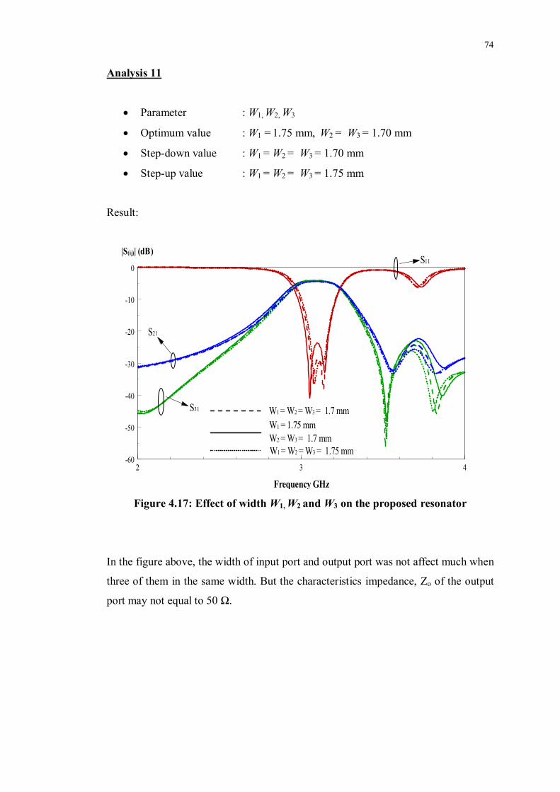
Analysis 11
Parameter : W1, W2, W3
Optimum value : W1 = 1.75 mm, W2 = W3 = 1.70 mm
Step-down value : W1 = W2 = W3 = 1.70 mm
Step-up value : W1 = W2 = W3 = 1.75 mm
Result:
2 3 4-60
-50
-40
-30
-20
-10
0
S21
S31
S11
Frequency GHz
|S(ij)| (dB)
W1 = W2 = W3 = 1.7 mmW1 = 1.75 mmW2 = W3 = 1.7 mmW1 = W2 = W3 = 1.75 mm
Figure 4.17: Effect of width W1, W2 and W3 on the proposed resonator
In the figure above, the width of input port and output port was not affect much when
three of them in the same width. But the characteristics impedance, Zo of the output
port may not equal to 50 Ω.
75
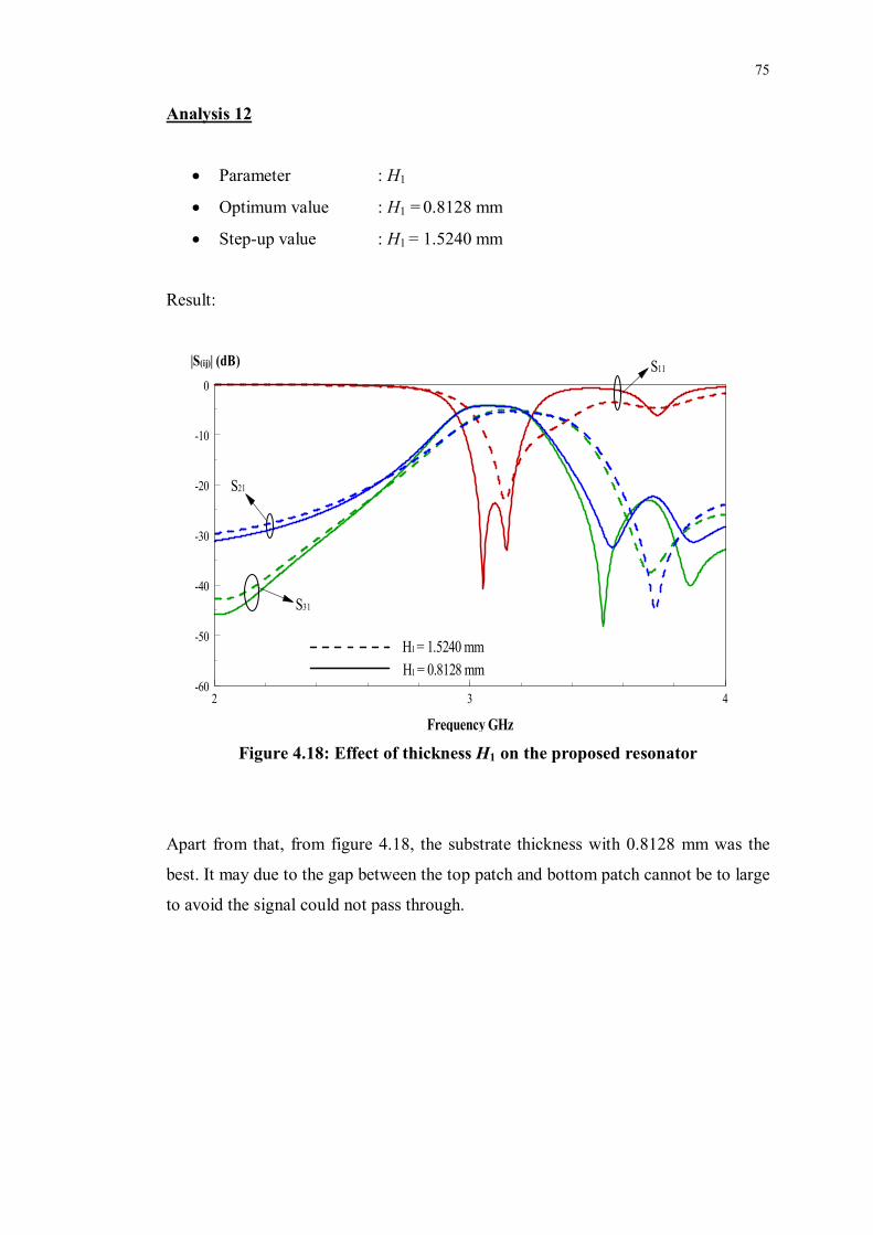
Analysis 12
Parameter : H1
Optimum value : H1 = 0.8128 mm
Step-up value : H1 = 1.5240 mm
Result:
2 3 4-60
-50
-40
-30
-20
-10
0
S21
S31
S11
Frequency GHz
|S(ij)| (dB)
H1 = 1.5240 mmH1 = 0.8128 mm
Figure 4.18: Effect of thickness H1 on the proposed resonator
Apart from that, from figure 4.18, the substrate thickness with 0.8128 mm was the
best. It may due to the gap between the top patch and bottom patch cannot be to large
to avoid the signal could not pass through.
76
Analysis 13
Parameter : G1
Optimum value : G1 = 0.5 mm
Step-down value : G1 = 0.2 mm
Step-up value : G1 = 1.0 mm
Result:
2 3 4-60
-50
-40
-30
-20
-10
0
S21
S31
S11
Frequency GHz
|S(ij)| (dB)
G1 = 0.2 mmG1 = 0.5 mmG1 = 1.0 mm
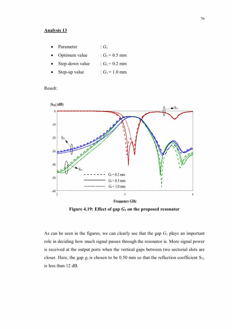
Figure 4.19: Effect of gap G1 on the proposed resonator
As can be seen in the figures, we can clearly see that the gap G1 plays an important
role in deciding how much signal passes through the resonator is. More signal power
is received at the output ports when the vertical gaps between two sectorial slots are
closer. Here, the gap g1 is chosen to be 0.50 mm so that the reflection coefficient S11
is less than 12 dB.

77
Analysis 14
Parameter : G2
Optimum value : G2 = 0.5 mm
Step-down value : G2 = 0.2 mm
Step-up value : G2 = 1.0 mm
Result:
2 3 4-60
-50
-40
-30
-20
-10
0
S21
S31
S11
Frequency GHz
|S(ij)| (dB)
G2 = 0.2 mmG2 = 0.5 mmG2 = 1.0 mm
Figure 4.20: Effect of gap G2 on the proposed resonator
Parameter G2 has the same effect as that for G1. More signal power is received at the
output ports when the horizontal gaps between two sectorial slots are closer. Here,
the gap G2 is chosen to be 0.50 mm so that the reflection coefficient S11 is less than
12 dB.
78
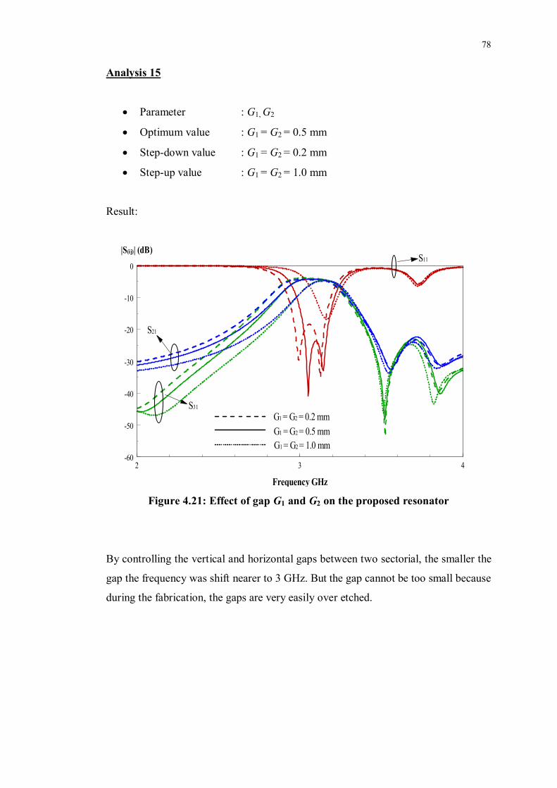
Analysis 15
Parameter : G1, G2
Optimum value : G1 = G2 = 0.5 mm
Step-down value : G1 = G2 = 0.2 mm
Step-up value : G1 = G2 = 1.0 mm
Result:
2 3 4-60
-50
-40
-30
-20
-10
0
S21
S31
S11
Frequency GHz
|S(ij)| (dB)
G1 = G2 = 0.2 mmG1 = G2 = 0.5 mmG1 = G2 = 1.0 mm
Figure 4.21: Effect of gap G1 and G2 on the proposed resonator
By controlling the vertical and horizontal gaps between two sectorial, the smaller the
gap the frequency was shift nearer to 3 GHz. But the gap cannot be too small because
during the fabrication, the gaps are very easily over etched.

79
CHAPTER 5
5 CONCLUSION AND RECOMMENDATIONS
5.1 Achievement
In this project, a broadside-coupled patch directional coupler has been proposed and
investigated in Chapter 3. By using proposed directional coupler shown in figure 3.1,
a two-mode directional coupler can be designed. Idea was demonstrated on the
RO4003C substrate. Experimental data are compared with the simulation results.
Fractional bandwidth difference between experimental and simulation is 9.2% which
is less than 10%. This two-mode directional coupler has wideband performance and
two poles in S11.
A travelling-wave sectorial slot resonator has been proposed and discussion in
Chapter 4. Proposed design was further demonstrated on RO4003C substrate. The
simulation data were discussed by comparing parameter analysis due to experiments
is run out of time. A 12 dB return loss was achieved so that signal pass through the
device are not easy reflected back.
5.2 Future Work
As for the proposed multi-port directional, the coupling level very difficult to
maintain in 10 ± 1 dB during the experiment stages. It may due the alignment of the
layer which is not same as simulation alignment. Therefore, as for future

80
improvement, the coupled line can be separated to two U-shaped to make the circuit
compact. So the circuit total has six-port directional coupler to achieved better
coupling level.
For the proposed resonator, design can be improve by using smaller size of substrate
such as 50 x 50 mm which can save the cost of board. Apart from that, to achieve the
center frequency at 3 GHz, top and bottom patch should enlarge. This proposed
resonator can be a strong travelling wave if center frequency meets the Federal
Communications Commission (FCC) requirement.
5.3 Conclusion
Both broadside-coupled patch directional coupler and travelling-wave slot resonator
have been designed and demonstrated in this project. For the proposed directional
coupler, experimental results agree well with the simulation results. While, for
proposed resonator, only simulation can be done. Experiments cannot be finis due to
author is run out of time. In this thesis, design considerations and issues of the
proposed directional coupler and resonator have also been studied. The objectives of
this project have been met.
81
REFERENCES
Directional Couplers. (n.d.). Retrieved August 17, 2012, from Microwave
Encylopedia: www.microwaves101.com/encyclopedia/directionalcouplers.cfm.
Pozar, D. M. (1998). Microwave Engineering . Canada: John Wiley & Sons, Inc.
S.N.A.M. Ghazali, N.Seman, R.C. Yob, M.K.A. Rahim and S.K.A.Rahim.
(November 2011). Design and Cross-Section Analysis of Wideband Rectangular-
Shaped Directional Coupler. IEEE transaction on Microwave Theory and
Techniques.
H.-J. Yuan and Y. Fan. (November 2011). Compact Microstrip Dual-band Filter with
Stepped-impedance Resonators. Electronic Letters.
Ferdinando Alesssandri, Marco Giordano, Marco Guglielmi, Giacomo Martirano,
Francesco Vitulli. (May 2003). A New Multiple-Tuned Six-Port Riblet-Type
Directional Coupler in Rectangular Waveguide. IEEE Transactions on Microwave
Theory and Techniques , Vol. 51, No.5.
Chang, K. RF and Microwave Wireless System. New York/ Chichester/ Weinheim/
Brisbane/ Singapore/ Toronto: John Wiley & Sons, Inc.
Introduction to RF & Wireless Communications Systems. (n.d.). Retrieved August 18,
2012, from National Instruments: http://www.ni.com/white-paper/3541/en.
Microstrip. (n.d.). Retrieved August 18, 2012, from Wikipedia:
http://en.wikipedia.org/wiki/Microstrip.
82
Hong J. S. & M.J. Lancaster. . (2001). Microstrip Filtter for RF/Microwave
Applications. New York/ Chichestor/ Weinheim/ Brisbane/ Singapore/ Toronto: John
Wiley & Sons, Inc.
J.K. Shimizu, E. M. T. Jones. (1958). Coupled-Transmission-Line Directional
Coupler. IEEE Transactions on Microwave Theory and Techniques , 404.
Resonator. (n.d.). Retrieved August 20, 2012, from Wikipedia:
http://en.wikipedia.org/wiki/Resonator.
Chapter 6 Microwave Resonators. (n.d). Retrieved August 21, 2012, from:
http://cc.ee.ntu.edu.tw/~thc/course_mckt/note/note5.pdf.
An Introduction to Microwave Technology. (n.d). Retrieved August 21, 2012, from:
http://www.invictusnetworks.com/faq/RF%20Technical%20Info%20and%20FCC%
20Regs/An%20Introduction%20to%20Microwave%20Technology.pdf.
Charactreristic impedance (n.d), obtained at 25 August 2012,
http://en.wikipedia.org/wiki/Characteristic_impedance
Microstrip Substrate Relative Dielectric Constant (December 2007), obtained at 26
August 2012. http://www.mwrf.com/Articles/Index.cfm?Ad=1&ArticleID=17725
Juan Enrique Page, Jaime Esteban and Carlos Camacho-Penalosa. (n.d.). Lattice
Equivalent Circuits of Transmission-Line and Coupled-Line Section. IEEE
Transaction on Microwave Theory and Techniques
Bian Wu, Wen Su, Shou-jia Sun and Chang-Hong Liang. (November 2011). Novel
Dual-mode Bandpass Filter Using Slot-line Square Loop Resonator. IEEE
transaction on Microwave Theory and Techniques.
C. –C. Chang, C. Caloz and T. Itoh. (2011). Analysis of a Compact Slot Resonator in
the Ground Plane for Microstrip Structures. IEEE transaction on Microwave Theory
and Techniques.

83
J-L. Li, S.-W Qu and Q. Xue. (February 2007). Microstrip directional coupler with
flat coupling and high isolation. Electronic Letters , Vol. 43, No. 4.
Ravi Kumar, Rajesh Kumar Vishwakarma and Ashutosh Singh. (2008). Analysis of
Aperture Coupled Multilayered Microstrip Directional Coupler. IEEE transaction on
Microwave Theory and Techniques.
Ruscito and Elizabeth. (September 2011). Application of a High Q, Low Cost
Hemispherical Cavity Resonator to Microwave Oscillators. ProQuest Dissertation
and Thesis.
Kun Song, Yingzeng Yin, Shoutao Fan and Yuqing Wei. (2011). Compact UWB
Band-pass Filter with Ring Slot Resonator Structure for Improved Upper Stop-band
Suppression Characteristic. IEEE transaction on Microwave Theory and Techniques.