Diodes Incorporated Discrete and Analog Semiconductors ... 2181 REV 01_1.pdf · Diodes Incorporated...
17
Diodes Incorporated Discrete and Analog Semiconductors Qualification Report – PCN-2181 Manufacturer No.: Conversion to Copper Bond Wire, Additional A/T site, and/or Additional Wafer Source with Smaller Die Size on Selected Discrete Products Revision: 0 Date: February 23, 2016 Qualified By: Diodes Incorporated Also Applicable To: The part numbers listed in the associated PCN are Qualified by Similarity (QBS) to the devices included in this report. Please go to www.diodes.com for current data sheets on associated devices Prepared By: Diodes US Document Control Date February 23, 2016 Approved By: Diodes US QRA Department Date February 23, 2016 The information contained herein is DIODES INCORPORATED PROPRIETARY information. Reproduction of this document, disclosure of the information, and use for any purpose other than the conduct of business with Diodes is expressly prohibited DIODES INCORPORATED 4949 Hedgcoxe Road, Suite # 200, Plano, TX 75024 USA www.diodes.com
Transcript of Diodes Incorporated Discrete and Analog Semiconductors ... 2181 REV 01_1.pdf · Diodes Incorporated...

Diodes Incorporated Discrete and Analog Semiconductors
Qualification Report – PCN-2181
Manufacturer No.: Conversion to Copper Bond Wire, Additional A/T site, and/or Additional Wafer Source with Smaller Die Size on Selected Discrete Products
Revision: 0
Date: February 23, 2016
Qualified By: Diodes Incorporated
Also Applicable To: The part numbers listed in the associated PCN are Qualified by Similarity (QBS) to the devices included in this report.
Please go to www.diodes.com for current data sheets on associated devices
Prepared By: Diodes US Document Control Date February 23, 2016
Approved By: Diodes US QRA Department Date February 23, 2016
The information contained herein is DIODES INCORPORATED PROPRIETARY information. Reproduction of this document, disclosure of the information, and use for any purpose other than the conduct of business with Diodes is expressly prohibited DIODES INCORPORATED 4949 Hedgcoxe Road, Suite # 200, Plano, TX 75024 USA www.diodes.com

Quality and Reliability Data Notice Plastic encapsulated Diodes Incorporated semiconductor devices are not designed and are not warranted to be suitable for use in some military applications and/or military environments. Use of plastic encapsulated Diodes Incorporated semiconductor devices in military applications and/or military environments, in lieu of hermetically sealed ceramic devices, is understood to be fully at the risk of Buyer. Quality and reliability data provided by Diodes Incorporated is intended to be an estimate of product performance based upon history only. It does not imply that any performance levels reflected in such data can be met if the product is operated outside the conditions expressly stated in the latest published data sheet for a device. Existing industry standards for plastic encapsulated microcircuit qualification and reliability monitors are based upon historical data, experiments, and field experience with the use of these devices in commercial and industrial applications. The applicability of these standards in determining the suitability for use and safety performance in life support, military and aerospace applications has not been established. Due to the multiple variations in field operating conditions, a component manufacturer can only base estimates of product life on models and the results of package and die level qualification. The buyer’s use of this data, and all consequences of such use, is solely the buyer’s responsibility. Buyer assumes full responsibility to perform sufficient engineering and additional qualification testing in order to properly evaluate the buyer’s application and determine whether a candidate device is suitable for use in that application. The information provided by Diodes Incorporated shall not be considered sufficient grounds on which to base any such determination. THIS INFORMATION IS PROVIDED "AS IS" WITHOUT ANY EXPRESS OR IMPLIED WARRANTY OF ANY KIND INCLUDING WARRANTIES OF MERCHANTABILITY, NONINFRINGEMENT OF INTELLECTUAL PROPERTY, OR FITNESS FOR ANY PARTICULAR PURPOSE. IN NO EVENT SHALL DIODES INCORPORATEDOR ITS SUPPLIERS BE LIABLE FOR ANY DAMAGES WHATSOEVER (INCLUDING, WITHOUT LIMITATION, DAMAGES FOR LOSS OF PROFITS, BUSINESS INTERRUPTION, LOSS OF INFORMATION) ARISING OUT OF THE USE OF OR INABILITY TO USE THE INFORMATION, EVEN IF DIODES INCORPORATED HAS BEEN ADVISED OF THE POSSIBILITY OF SUCH DAMAGES. Diodes Incorporated may provide technical, applications or design advice, quality characterization, and reliability data or service providing these items shall not expand or otherwise affect Diodes Incorporated warranties as set forth in the Diodes Incorporated Standard Terms and Conditions of Sale for and no obligation or liability shall arise from Diodes Incorporated provision of such items.
"The information contained herein is DIODES INCORPORATED PROPRIETARY information. Reproduction of this document, disclosure of the information, and use for any purpose other than the conduct of business with Diodes
Incorporated is expressly prohibited".
DIODES INCORPORATED 4949 Hedgcoxe Road, Suite # 200
Plano, TX 75024 USA (972) 987-3900
www.diodes.com

________________________________________________________________________
DIC-034 R3 Page 1 of 3
Diodes Incorporated Rel Date: 2/10/2016
www.diodes.com
DATE: 23rd February, 2016
PCN #: 2181
PCN Title: Conversion to Copper Bond Wire, Additional A/T site, and/or Additional Wafer Source with Smaller Die Size on Selected Discrete Products
Dear Customer: This is an announcement of change(s) to products that are currently being offered by Diodes Incorporated. We request that you acknowledge receipt of this notification within 30 days of the date of this PCN. If you require samples for evaluation purposes, please make a request within 30 days as well. Otherwise, samples may not be built prior to this change. Please refer to the implementation date of this change as it is stated in the attached PCN form. Please contact your local Diodes sales representative to acknowledge receipt of this PCN and for any sample requests. The changes announced in this PCN will not be implemented earlier than 90 days from the notification date stated in the attached PCN form. Previously agreed upon customer specific change process requirements or device specific requirements will be addressed separately. For questions or clarification regarding this PCN, please contact your local Diodes sales representative. Sincerely, Diodes Incorporated PCN Team

________________________________________________________________________
DIC-034 R3 Page 2 of 3
Diodes Incorporated Rel Date: 2/10/2016
www.diodes.com
PRODUCT CHANGE NOTICE
PCN-2181 REV 00
Notification Date: Implementation
Date: Product Family: Change Type: PCN #:
23rd February, 2016 22nd May, 2016 Discrete
Semiconductors
Bond Wire Material / Wafer FAB Material / Additional
Assembly & Test Site 2181
TITLE
Conversion to Copper Bond Wire, Additional A/T site, and/or Additional Wafer Source with Smaller Die Size on Selected Discrete Products
DESCRIPTION OF CHANGE
This PCN is being issued to notify customers that Diodes has qualified Copper bond wire for the selected Discrete products listed in this PCN. In order to accommodate the Copper bond wire, the top metal composition and/or top metal thickness of the wafer has been modified. Diodes Incorporated has also qualified an additional wafer source with smaller die size, Diodes internal FabTech Inc. (KFAB) or external Phenitec Semiconductor (*), and qualified “Diodes Technology (Chengdu) Company Limited” (CAT) as an additional Assembly & Test Site (A/T Site) for the selected Discrete products.
Full electrical characterization and high reliability testing has been completed on representative part numbers built using Copper bond wire, alternative wafer source and/or additional A/T site to ensure no change to device functionality or electrical specifications in the datasheet.
There will be no change to the Form, Fit, or Function of affected products.
IMPACT
There is no change in datasheet parameters and product performance.
PRODUCTS AFFECTED
Please refer to Table 1 for Cu bond wire conversion
Please refer to Table 2 for Cu bond wire conversion and additional wafer source with smaller die size
Please refer to Table 3 for additional A/T site and additional wafer source with smaller die size
Please refer to Table 4 for additional wafer source with smaller die size
WEB LINKS
Manufacturer’s Notice: http://www.diodes.com/quality/pcns
For More Information Contact: http://www.diodes.com/contacts
Data Sheet: http://www.diodes.com/products
DISCLAIMER
Unless a Diodes Incorporated Sales representative is contacted in writing within 30 days of the posting of this notice, all changes described in this announcement are considered approved.

________________________________________________________________________
DIC-034 R3 Page 3 of 3
Diodes Incorporated Rel Date: 2/10/2016
www.diodes.com
Table 1 - Cu Bond Wire Conversion
DCX114EU-7-F DDC114TU-7-F DDTA144WE-7-F DCX114EH-7 ZUMT718TA
DCX114TU-7-F DDC114YU-7-F DDTC113ZE-7-F DDA114EH-7 ZUMT720TA
DCX114YU-7-F DDC123JU-7-F DDTC114EE-7-F DDA114TH-7 BC817-40W-7
DCX123JU-7-F DDC124EU-7-F DDTC114GE-7-F DDA114YH-7 MMST5401-7-F
DCX124EU-7-F DDC143TU-7-F DDTC114YE-7-F DDA124EH-7 MMST5551-7-F
DCX143EU-7-F DDC144EU-7-F DDTC115EE-7-F DDC114EH-7 MMST6427-7-F
DCX143TU-7-F DDC144NS-7 DDTC122LE-7-F DDC114YH-7 MMSTA13-7-F
DCX144EU-7-F DDC144TU-7 DDTC123JE-7-F DDC123JH-7 MMSTA14-7-F
DDA113TU-7-F DDTA113TE-7-F DDTC123YE-7-F DDC142TH-7 MMSTA42-7-F
DDA114EU-7-F DDTA113ZE-7-F DDTC124EE-7-F DDC143TH-7 MMSTA55-7-F
DDA114TU-7-F DDTA114EE-7-F DDTC124XE-7-F ZUMT491TA MMSTA56-7-F
DDA114YU-7-F DDTA114WE-7-F DDTC143EE-7-F ZUMT591TA MMSTA92-7-F
DDA123JU-7-F DDTA123JE-7-F DDTC143TE-7-F ZUMT617TA 2DB1689-7
DDA143TU-7-F DDTA123YE-7-F DDTC143XE-7-F ZUMT618TA 2DB1694-7
DDA144EU-7-F DDTA143EE-7-F DDTC143ZE-7-F ZUMT619TA 2DD2652-7
DDC113TU-7-F DDTA143TE-7-F DDTC144EE-7-F ZUMT619TC 2DD2656-7
DDC114EU-7-F DDTA144EE-7-F DDTC144WE-7-F ZUMT717TA T6V0S5-7
Table 2 - Cu Bond Wire Conversion and Additional Wafer Source with Smaller Dies Size
MMBT2907AT-7-F MMDT2222V-7 MMDT2907V-7 MMDT3906VC-7 MMBT3906T-13-F
MMBT2222A-7-G DLP05LC-7-F*
* Phenitec Semiconductor as an additional wafer source
Table 3 - Additional A/T site and Additional Wafer Source with Smaller Die Size
MMDT4124-7-F MMDT3946-7-F MMBT4126-7-F MMBT3904-13-F DMMT3904W-7-F
MMDT3906-7-F MMDT4146-7-F MMDT3904-7-F MMBT3906-13-F DMMT3906W-7-F
MMDT4126-7-F MMBT4124-7-F MMDT2907A-7-F
Table 4 - Additional Wafer Source with Smaller Die Size
MMBT2222AT-7-F MMDT3904VC-7 MMST3904-7-F MMST4126-7-F MMBT2907A-13-F
MMBT3904T-7-F MMDT2222A-7-F MMST3906-7-F MMBT3904-7-F MMBT2907A-7-F
MMBT3906T-7-F MMDT2227-7-F MMST4124-7-F MMBT3906-7-F MMDT2227M-7
MMDT3904V-7 MMST2907A-7-F

Certificate of Design, Construction & Qualification
Description: Qualification of the KFAB C2222S die at SAT across all packages
Category Qual Device 1 Qual Device 2 Qual Device 4 Qual Device 5
Product Part Number MMBT2222A MMDT2222A MMDT2222V MMBT2222ALP4
Assembly Package Type SOT‐23 SOT‐363 SOT‐563 X2‐DFN1006‐3
Assembly Package Size (mm) 2.9 x 1.3 x 0.975 2.0 x 1.25 x 0.95 1.6 x 1.2 x 0.6 1.0 x 0.6 x 0.4
Wafer Die Name(s) C2222S C2222S C2222S C2222S
Wafer Die Size (W/L/Thickness) ‐ After Saw 348 x 348 x 216 um 348 x 348 x 216 um 348 x 348 x 216 um 348 x 348 x 216 um
Wafer Die Process / Technology Bipolar Bipolar Bipolar Bipolar
Wafer Wafer FAB/ Location KFAB / Kansas KFAB / Kansas KFAB / Kansas KFAB / Kansas
Wafer Wafer Diameter 150mm 150mm 150mm 150mm
Wafer Front Metal Type AlSiCu AlSiCu AlSiCu AlSiCu
Wafer Front Metal Layer Number/ Thickness 3.5um 3.5um 3.0um 3.0um
Wafer Number of Poly Layers none none none none
Wafer Back Metal Type (All Layers) NiV‐Au NiV‐Au NiV‐Au NiV‐Au
Wafer Back Metal Thickness (All Layers) NiV(125A)+Au(5150A) NiV(125A)+Au(5150A) NiV(125A)+Au(5150A) NiV(125A)+Au(5150A)
Wafer Die Conforming Coating (Passivation) Oxide / Nitride Oxide / Nitride Oxide / Nitride Oxide / Nitride
Wafer Die passivation thickness range OX 6000A / NIT 1500A OX 6000A / NIT 1500A OX 6000A / NIT 1500A OX 6000A / NIT 1500A
Wafer No of masks Steps 5 5 5 5
Assembly Die quantity per package (e.g. single or dual dies) 1 2 2 1
Assembly Die Attach Method (DB Epoxy/Solder Type) Eutectic Eutectic Eutectic Epoxy
Assembly Die Attach Material/ Supplier n/a n/a n/a QMI519
Assembly Bond Wire/Clip Bond Material/ Supplier Cu Cu Cu Au
Assembly Bond Type (at Die) Thermosonic Thermosonic Thermosonic Thermosonic
Assembly Bond Type (at LF) Thermosonic Thermosonic Thermosonic Thermosonic
Assembly No. of bond over active area 2 4 2 2
Assembly Glass Transistion Temp 130 130 130 130
Assembly Terminal Finish (Plating) Material Matte Sn Matte Sn Matte Sn NIPdAu
Assembly Header plating (Die Land Area) Spot Ag Spot Ag Spot Ag Spot Ag
Assembly Wire Diameter 1 mil 1 mil 1 mil 0,8mil
Assembly Leadframe Type SOT‐23A SOT‐363E SOT‐563E SLP1006P3
Assembly Leadframe Material Alloy42 Alloy42 EFTEC‐64T C7025HH
Assembly Lead Frame Manufacturer PBE/XMYH/JYKQ/JihLin PBE/XMYH/JYKQ/JihLin MHT MHT
Assembly Molding Compound Type GR640HV‐L1 CEL‐1702HF9 SK CEL‐1702HF9 SK EME‐G770HCD
Assembly Mold Compound Material Manufacturer HenKel HITACHI HITACHI SUMITOMO
Assembly Green Compound (Yes/No) Yes Yes Yes Yes
Assembly Lead‐Free (Yes/No) Yes Yes Yes Yes
Assembly Assembly Site/ Location SAT / Shanghai SAT / Shanghai SAT / Shanghai SAT / Shanghai
Assembly Test Site/ Location SAT / Shanghai SAT / Shanghai SAT / Shanghai SAT / Shanghai
Product Max Junction Temp 150°C 150°C 150°C 150°C
Product Max Thermal resistance Junc (amibent) 403°C/W 625°C/W 833°C/W 272°C/W
Product DataSheet DS30041 DS30125 DS30563 DS35506
Reliability and Characterization Testing
# in AEC‐
Q101
(D)
Test Test Conditions Duration / Limits
Accept on #
Failed/
Sample
Size per Lot
# of Lots X = Test NeededResults
Pass/FailX = Test Needed
Results
Pass/FailQBS Test Completed
Results
Pass/FailQBS Test Completed
Results
Pass/Fail
Bake 125C 24 Hrs X Pass X Pass X Pass X PassSoak 85C, 85% RH 168Hrs X Pass X Pass X Pass X Pass
IR reflow 260C 3 cycles X Pass X Pass X Pass X Pass
3EXTERNAL VISUAL
(EV)MIL‐STD‐750 METHOD 2071 PER SPEC X Pass X Pass X Pass X Pass
4PARAMETRIC
VERIFICATION (PV)‐55C, 25C, 85C, 125C, 150C
Operating Range,
Per Data Sheet0/25 3 wafer lots X Pass X Pass X Pass X Pass
168 Hrs 0/77 X Pass X Pass X Pass X Pass
500 Hrs 0/77 X Pass X Pass X Pass X Pass1000 Hrs 0/77 X Pass X Pass X Pass X Pass
168 Cycles 0/77 X Pass X Pass X Pass X Pass
500 Cycles 0/77 X Pass X Pass X Pass X Pass1000 Cycles 0/77 X Pass X Pass X Pass X Pass
8 PCT/AC Ta=121 15PSIG 100%RH; PER JESD22‐
A10296 Hrs 0/77 3 Assembly lots X Pass X Pass X Pass X Pass
9 HAST Ta=130C, 85%RH 33.3 psia 80% Bias; PER JESD22‐
A11096 Hrs 0/77 3 wafer lots X Pass X Pass X Pass
168 Hrs 0/77 X Pass
500 Hrs 0/77 X Pass1000 Hrs 0/77 X Pass
2520 Cycles 0/77 X Pass X Pass X Pass X Pass
7560 Cycles 0/77 X Pass X Pass X Pass X Pass15000 Cycles 0/77 X Pass X Pass X Pass X Pass
HBM (AEC‐Q101‐001) PER DATA SHEET 0/30 1 wafer lot X Pass X Pass X Pass X Pass
MM ( AEC‐Q101‐002) PER DATA SHEET 0/30 1 wafer lot X Pass X Pass X Pass X Pass
12 DPA AEC Q101‐004 SEC. 4 0/2 1 Assembly lot X Pass X Pass X Pass X Pass
22THERMAL
RESISTANCE (TR)JESD 24‐3, 24‐4, 24‐6 AS APPROPRIATE PER SPEC 0/10 1 Assembly lot X Pass X Pass X Pass X Pass
23 Wire Bond Strength MIL‐STD‐750 METHOD 2037 (JESD22‐B116B) Cpk>1.66 0/ min of 5 1 Assembly lot X Pass X Pass X Pass X Pass
24 BOND SHEAR AEC‐Q101‐003 Cpk>1.66 0/ min of 5 1 Assembly lot X Pass X Pass X Pass X Pass
25 Die Shear MIL‐STD‐750 (2017) Cpk>1.66 0/5 1 Assembly lot X Pass X Pass X Pass X Pass
Summary: ____________________________________
Submitted By: Jon Stocker
Approved By:
3 Assembly lots
3 wafer lots
3 wafer lots
All qualification parts submitted for
testing
SMD only,
for Test #7,
8, 9 & 10
3 Assembly lots
3 wafer lots
ESD
MSL1 Pre‐
conditioning
IOL
TC
H3TRB
HTRB
11
2
10
7
9 alt
5
MIL‐STD‐750 Method 1037 (N/A for TVS)
Ta=‐65C to 150C or Max Tj, PER JESD22A‐104
Ta=85ºC, 85% RH, with 80% Maximum Reverse
Bias. JESD22A‐101
Ta=150 or Max Tj, Vd/Vr/Vcbo=80%, MIL‐STD‐
750‐1 / PER JESD22 A‐108

Certificate of Design, Construction & Qualification
Description:
Category Qual Device 1 Qual Device 2 Qual Device 3 Qual Device 4 Qual Device 5
Product Part Number MMST3904 MMDT3904 MMBT3904T MMDT3904V DXT3904
Assembly Package Type SOT‐323 SOT‐363 SOT‐523 SOT‐563 SOT‐89
Assembly Package Size 2.0 x 1.25 2.15 x 1.3 1.6 x 0.8 1.6 x 1.2 4.5 x 2.5
Wafer Die Name(s) C3904S C3904S C3904S C3904S C3904S
Wafer Die Size (W/L/Thickness) ‐ After Saw 278x278x216 260x260x216 260x260x216 260x260x216 260x260x216
Wafer Die Process / Technology Small signal BJT Small signal BJT Small signal BJT Small signal BJT Small signal BJT
Wafer Wafer FAB KFAB KFAB KFAB KFAB KFAB
Wafer Wafer Diameter 150mm 150mm 150mm 150mm 150mm
Wafer Front Metal Type AlSiCu AlSiCu AlSiCu AlSiCu AlSiCu
Wafer Front Metal Thickness 3.5um 3.5um 3.5um 3.5um 3.5um
Wafer Back Metal Type (All Layers) NiV‐Au NiV‐Au NiV‐Au NiV‐Au NiV‐Au
Wafer Back Metal Thickness (All Layers) 300/2600/5500A 300/2600/5500A 300/2600/5500A 300/2600/5500A 300/2600/5500A
Wafer Die Conforming Coating (Passivation) OX/NIT OX/NIT OX/NIT OX/NIT OX/NIT
Wafer Die passivation thickness range OX 6000A / NIT 1500A OX 6000A / NIT 1500A OX 6000A / NIT 1500A OX 6000A / NIT 1500A OX 6000A / NIT 1500A
Wafer No of masks Steps 5 5 5 5 5
Assembly Die quantity per package (e.g. single or dual dies) 1 2 1 2 1
Assembly Die Attach Method (DB Epoxy/Solder Type) Eu Eu Eu Eu Epoxy
Assembly Die Attach Material N/A N/A N/A N/A 8200TI
Assembly Bond Wire/Clip Bond Material Cu Cu Cu Cu Cu
Assembly Bond Type (at Die) Thermosonic Thermosonic Thermosonic Thermosonic Thermosonic
Assembly Bond Type (at LF) Thermosonic Thermosonic Thermosonic Thermosonic Thermosonic
Assembly No. of bond over active area 2 4 2 4 2
Assembly Glass Transistion Temp 130C 130 130 130 130
Assembly Terminal Finish (Plating) Material matt Sn matt Sn matt Sn matt Sn Mat Sn
Assembly Header plating (Die Land Area) Spot Ag Spot Ag Spot Ag Spot Ag Spot Ag
Assembly Wire Diameter 1 mil 1 mil 1 mil 1 mil 1 mil
Assembly Leadframe Type SOT‐323A SOT‐363E SOT‐523A SOT‐563D SOT‐89 3 lead
Assembly Leadframe Material Alloy 42 Alloy 42 Alloy 42 EFTEC‐64T CDA194HH
Assembly Lead Frame Manufacturer PBE/JihLin/ASM PBE/JihLin/ASM PBE/JihLin/ASM MHT PBE/HITACHI
Assembly Molding Compound Type CEL‐1702HF9 SK CEL‐1702HF9 SK CEL‐1702HF9 SK CEL‐1702HF9 SKF EME‐G600
Assembly Mold Compound Material Manufacturer HITACHI HITACHI HITACHI HITACHI SUMITOMO
Assembly Green Compound (Yes/No) yes yes yes yes yes
Assembly Lead‐Free (Yes/No) yes yes yes yes yes
Assembly Assembly Site SAT SAT SAT SAT SAT
Assembly Test Site SAT SAT SAT SAT SAT
Product Max Junction Temp 150C 150C 150C 150C 150C
Product Max Thermal resistance Junc (amibent) 625°C/W 625°C/W 833°C/W 625°C/W 125°C/W
Product DataSheet DS300082 DS300088 DS30270 DS30636 DS31141
Reliability and Characterization Testing# in
AEC‐
Q101
(D)
Test Test Conditions Duration / Limits
Fail/SS ‐
Sample
Size
X = Test NeededResults
Pass/FailX = Test Needed
Results
Pass/FailX = Test Needed
Results
Pass/FailX = Test Needed
Results
Pass/FailX = Test Needed
Results
Pass/Fail
Bake 125C 24 Hrs 0/385 X Pass X Pass X Pass X Pass X Pass
Soak 85C, 85% RH 168Hrs 0/385 X Pass X Pass X Pass X Pass X Pass
IR reflow 260C 3 cycles 0/385 X Pass X Pass X Pass X Pass X Pass
3EXTERNAL VISUAL
(EV)MIL‐STD‐750 METHOD 2071 PER SPEC 0/500 X Pass X Pass X Pass X Pass X Pass
4
PARAMETRIC
VERIFICATION
(PV)
‐55C, 25C, 85C, 125C, 150COperating Range,
Per Data Sheet0/25 X Pass X Pass X Pass X Pass X Pass
168 Hrs 0/77 X Pass
500 Hrs 0/77 X Pass
1000 Hrs 0/77 X Pass
168 Hrs 0/77 X Pass X Pass X Pass X Pass
500 Hrs 0/77 X Pass X Pass X Pass X Pass
1000 Hrs 0/77 X Pass X Pass X Pass X Pass
168 Cycles 0/77 X Pass X Pass X Pass X Pass X Pass
500 Cycles 0/77 X Pass X Pass X Pass X Pass X Pass
1000 Cycles 0/77 X Pass X Pass X Pass X Pass X Pass
9 HAST 130C, 85%RH 33.3 psia 80% Bias 96 Hrs 0/77 X Pass
168 Hrs 0/77 X Pass X Pass X Pass X Pass500 Hrs 0/77 X Pass X Pass X Pass X Pass1000 Hrs 0/77 X Pass X Pass X Pass X Pass
8 alt PCT/AC T=121 15PSIG 100%RH 96 Hrs 0/77 X Pass X Pass X Pass X Pass
2520 Cycles 0/77 X Pass X Pass X Pass X Pass X Pass
7560 Cycles 0/77 X Pass X Pass X Pass X Pass X Pass
15000 Cycles 0/77 X Pass X Pass X Pass X Pass X Pass
HBM (AEC‐Q101‐001) PER DATA SHEET 0/30 X Pass X Pass X Pass X Pass X Pass
MM ( AEC‐Q101‐002) PER DATA SHEET 0/30 X Pass X Pass X Pass X Pass X Pass
12 DPA AEC Q101‐004 SEC. 4 0/2 X Pass X Pass X Pass X Pass X Pass
20
RESISTANCE TO
SOLDER HEAT
(RSH)
JESD22 B‐106 (260C @30S) PER SPEC 0/30 X Pass X Pass X Pass X Pass X Pass
21 Solderability J‐STD‐002 (245C +0/5S) 5 Seconds 0/10 Pass Pass Pass
22THERMAL
RESISTANCE (TR)JESD 24‐3, 24‐4, 24‐6 AS APPROPRIATE PER SPEC 0/10 X Pass X Pass X Pass X Pass X Pass
23Wire Bond
StrengthMIL‐STD‐750 METHOD 2037 (JESD22‐B116B) Cpk>1.66 0/30 X Pass X Pass X Pass X Pass X Pass
24 BOND SHEAR AEC‐Q101‐003 Cpk>1.66 0/30 X Pass X Pass X Pass X Pass X Pass
25 Die Shear MIL‐STD‐750 (2017) Cpk>1.66 0/30 X Pass X Pass X Pass X Pass X Pass
Summary: ____________________________________
Submitted By: Jon Stocker
Approved By:
IOL
TC
H3TRB
ESD
MSL1 Pre‐
conditioning
HTRB
HTRB
11
5
2
10
7
9 alt
5‐1
Qualification of KFAB C3904S die across SAT Packages
T=150 Vd=100%, PER JESD22 A‐108
MIL‐STD‐750 Method 1037 (N/A for TVS)
‐65C to 150C PER JESD22A‐104
TA=85ºC, 85% RH, with 80% Reverse bias.
JESD22A‐101
T=150 Vd=80%, PER JESD22 A‐108

Certificate of Design, Construction & Qualification
Description: qualification of C3906S die in SOT363, SOT23, SOT323 packages at CAT
Category Qual Device 1 Qual Device 2 Qual Device 3
Product Part Number DMMT3906W‐7‐F MMBT3906‐7‐F MMST3906‐7‐F
Assembly Package Type SOT‐363 SOT‐23 SOT‐323
Assembly Package Size 2.15x1.3x1.0mm 2.9 x1.3x0.975mm 2.15x1.3x0.95mm
Wafer Die Name(s) C3906S C3906S C3906S
Wafer Die Size (W/L/Thickness) ‐ After Saw 0.284 x 0.284 x 0.216 0.284 x 0.284 x 0.216 0.284 x 0.284 x 0.216
Wafer Die Process / Technology Bipolar Bipolar Bipolar
Wafer Wafer FAB/ Location KFAB/Kansas KFAB/Kansas KFAB/Kansas
Wafer Wafer Diameter 150mm 150mm 150mm
Wafer Front Metal Type AlSiCu AlSiCu AlSiCu
Wafer Front Metal Layer Number/ Thickness 3.5Um 3.5Um 3.5Um
Wafer Number of Poly Layers n/a n/a n/a
Wafer Back Metal Type (All Layers) NiV‐Au NiV‐Au NiV‐Au
Wafer Back Metal Thickness (All Layers) 300/2600/5500A 300/2600/5500A 300/2600/5500A
Wafer Die Conforming Coating (Passivation) Oxide / Nitride Oxide / Nitride Oxide / Nitride
Wafer Die passivation thickness range OX 6000A / NIT 1500A OX 6000A / NIT 1500A OX 6000A / NIT 1500A
Wafer No of masks Steps 5 5 5
Assembly Die quantity per package (e.g. single or dual dies) 2 1 1
Assembly Die Attach Method (DB Epoxy/Solder Type) Eutectic Eutectic Eutectic
Assembly Die Attach Material/ Supplier n/a n/a n/a
Assembly Bond Wire/Clip Bond Material/ Supplier Cu Cu Cu
Assembly Bond Type (at Die) Thermosonic Thermosonic Thermosonic
Assembly Bond Type (at LF) Thermosonic Thermosonic Thermosonic
Assembly No. of bond over active area 4 4 4
Assembly Glass Transistion Temp 110 130C 110
Assembly Terminal Finish (Plating) Material Matt Sn Matt Sn Matt Sn
Assembly Header plating (Die Land Area) Spot Ag Cu plate Spot Ag
Assembly Wire Diameter 0.8mm 0.8mm 0.8mm
Assembly Leadframe Type SOT‐363 18R SOT‐23C Copper plated LDF SOT‐323 H (Cu plated)
Assembly Leadframe Material ALLOY42 ALLOY42 ALLOY42
Assembly Lead Frame Manufacturer ASM / SDI ASM ASM / SDI
Assembly Molding Compound Type CEL‐1702HF9SK GR640HV CEL‐1702HF9SK
Assembly Mold Compound Material Manufacturer HITACHI HENKEL HITACHI
Assembly Green Compound (Yes/No) Yes Yes Yes
Assembly Lead‐Free (Yes/No) Yes Yes Yes
Assembly Assembly Site/ Location CAT / Chengdu CAT / Chengdu CAT / Chengdu
Assembly Test Site/ Location CAT / Chengdu CAT / Chengdu CAT / Chengdu
Product Max Junction Temp 150°C 150°C 150°C
Product Max Thermal resistance Junc (amibent) 625 °C/W 403°C/W 625 °C/W
Product DataSheet DS30312 DS300059 DS300082
Reliability and Characterization Testing
# in
AEC‐
Q101
(D)
Test Test Conditions Duration / Limits
Accept on #
Failed/
Sample
Size per Lot
# of Lots X = Test NeededResults
Pass/FailX = Test Needed
Results
Pass/FailX = Test Needed
Results
Pass/Fail
Bake 125C 24 Hrs X Pass X Pass X PassSoak 85C, 85% RH 168Hrs X Pass X Pass X Pass
IR reflow 260C 3 cycles X Pass X Pass X Pass
3EXTERNAL VISUAL
(EV)MIL‐STD‐750 METHOD 2071 PER SPEC X Pass X Pass X Pass
4PARAMETRIC
VERIFICATION (PV)‐55C, 25C, 85C, 125C, 150C
Operating Range,
Per Data Sheet0/25 3 wafer lots X Pass X Pass X Pass
168 Hrs 0/77 X Pass X Pass X Pass500 Hrs 0/77 X Pass X Pass X Pass1000 Hrs 0/77 X Pass X Pass X Pass
168 Cycles 0/77 X Pass X Pass X Pass500 Cycles 0/77 X Pass X Pass X Pass1000 Cycles 0/77 X Pass X Pass X Pass
8 PCT/AC Ta=121 15PSIG 100%RH; PER JESD22‐
A10296 Hrs 0/77 3 Assembly lots X Pass X Pass
9 HAST Ta=130C, 85%RH 33.3 psia 80% Bias; PER JESD22‐
A11096 Hrs 0/77 3 wafer lots X Pass X Pass
168 Hrs 0/77 X Pass500 Hrs 0/77 X Pass1000 Hrs 0/77 X Pass
2520 Cycles 0/77 X Pass X Pass X Pass
7560 Cycles 0/77 X Pass X Pass X Pass15000 Cycles 0/77 X Pass X Pass X Pass
HBM (AEC‐Q101‐001) PER DATA SHEET 0/30 1 wafer lot X Pass X Pass X Pass
MM ( AEC‐Q101‐002) PER DATA SHEET 0/30 1 wafer lot X Pass X Pass X Pass
12 DPA AEC Q101‐004 SEC. 4 0/2 1 Assembly lot X Pass X Pass X Pass
13Package Physical
Dimemsions (PD)JESD22‐B100 Package Outline 0/30 1 Assembly lot X Pass X Pass X Pass
20RESISTANCE TO
SOLDER HEAT (RSH)JESD22 A‐111 (SMD), B‐106 (PTH) (260C @30S) PER SPEC 0/30 1 Assembly lot X Pass X Pass X Pass
23 Wire Bond Strength MIL‐STD‐750 METHOD 2037 (JESD22‐B116B) Cpk>1.66 0/ min of 5 1 Assembly lot X Pass X Pass X Pass
24 BOND SHEAR AEC‐Q101‐003 Cpk>1.66 0/ min of 5 1 Assembly lot X Pass X Pass X Pass
25 Die Shear MIL‐STD‐750 (2017) Cpk>1.66 0/5 1 Assembly lot X Pass X Pass X Pass
168 Hrs 0/77 X Pass X Pass500 Hrs 0/77 X Pass X Pass1000 Hrs 0/77 X Pass X Pass
Summary: Final Report
Submitted By: Jon Stocker
Approved By:
MIL‐STD‐750 Method 1037 (N/A for TVS)
Ta=‐65C to 150C or Max Tj, PER JESD22A‐104
Ta=85ºC, 85% RH, with 80% Maximum Reverse
Bias. JESD22A‐101
Ta=150 or Max Tj, Vd/Vr/Vcbo=80%, MIL‐STD‐
750‐1 / PER JESD22 A‐108
2
10
7
9 alt
5
IOL
TC
H3TRB
HTRB
MSL1 Pre‐
conditioning
All qualification parts submitted for
testing
SMD only,
for Test #7,
8, 9 & 10
3 Assembly lots
3 wafer lots
3 Assembly lots
3 wafer lots
3 wafer lots
HS Ta=150ºC, 3 wafer lots
ESD11

Certificate of Design, Construction & Qualification
Qualification: KFAB C3906S Die Assembled at SAT in SOT23, SOT323, SOT363 and SOT523 Packages
TRB2013‐046 TRB2013‐046 TRB2014‐045 TRB2014‐045
Category Qual Device 1 Qual Device 2 Qual Device 3 Qual Device 4
Product Part Number MMBT3906‐7‐F MMBT3906‐7‐F MMBT3906‐7‐F MMBT3906T‐7‐F
Assembly Package Type SOT‐23 SOT‐23 SOT‐23 SOT‐523
Assembly Package Size 2.9 x 1.3 2.9 x 1.3 2.9 x 1.3 1.6 x 0.8
Wafer Die Name(s) C3906C (40um grid) C3906C (40um grid) C3906C (50um grid) C3906C (50um grid)
Wafer Die Size (W/L/Thickness) 0.26/0.26/0.215 0.26/0.26/0.215 0.26/0.26/0.215 0.284/0.284/0.215
Wafer Die Process / Technology SS BJT SS BJT SS BJT SS BJT
Wafer Wafer FAB KFAB KFAB KFAB KFAB
Wafer Wafer Diameter 150mm 150mm 150mm 150mm
Wafer Front Metal Type ALSiCu ALSiCu ALSiCu ALSiCu
Wafer Front Metal Thickness 3.5um 3.5um 3.5um 3.5um
Wafer Back Metal Type (All Layers) NiV‐Au NiV‐Au NiV‐Au NiV‐Au
Wafer Back Metal Thickness (All Layers) 125/5150A 125/5150A 125/5150A 125/5150A
Wafer Die Conforming Coating (Passivation) Oxide/Nitride Oxide/Nitride Oxide/Nitride Oxide/Nitride
Wafer Die passivation thickness range 6KA/1.5KA 6KA/1.5KA 6KA/1.5KA 6KA/1.5KA
Wafer No of masks Steps 6 6 6 6
Assembly Die quantity per package (e.g. single or dual dies) 1 1 1 1
Assembly Die Attach Method (DB Epoxy/Solder Type) Eutectic Eutectic Eutectic Eutectic
Assembly Die Attach Material n/a n/a n/a n/a
Assembly Bond Wire/Clip Bond Material Cu Cu Cu Cu
Assembly Bond Type (at Die) Thermosonic Thermosonic Thermosonic Thermosonic
Assembly Bond Type (at LF) Thermosonic Thermosonic Thermosonic Thermosonic
Assembly No. of bond over active area 2 2 2 2
Assembly Glass Transistion Temp 130 130 130 130
Assembly Terminal Finish (Plating) Material Matt Sn Matt Sn Matt Sn Matt Sn
Assembly Header plating (Die Land Area) Spot Ag Spot Ag Spot Ag Spot Ag
Assembly Wire Diameter 1 1 1 1
Assembly Leadframe Type SOT‐23A SOT‐23A SOT‐23A SOT‐523A
Assembly Leadframe Material Alloy42 Alloy42 Alloy42 Alloy42
Assembly Lead Frame Manufacturer MHL/PBE/NBKQ MHL/PBE/NBKQ MHL/PBE/NBKQ JihLin/ASM/NBKQ
Assembly Molding Compound Type GR640HV‐L1 GR640HV‐L1 GR640HV‐L1 CEL‐1702HF9 SK
Assembly Mold Compound Material Manufacturer Henkel Henkel Henkel Hitachi
Assembly Green Compound (Yes/No) Yes Yes Yes Yes
Assembly Lead‐Free (Yes/No) Yes Yes Yes Yes
Assembly Assembly Site SKE SKE SKE SKE
Assembly Test Site SKE SKE SKE SKE
Product Max Junction Temp 150°C 150°C 150°C 150°C
Product Max Thermal resistance Junc (amibent) 403°C/W 403°C/W 403°C/W 833°C/W
Product DataSheet DS300059 DS300059 DS300059 DS30271
Realibility and Characterization Testing
Test Test Conditions Duration / Limits Fail/SS X = Test NeededResults
Pass/FailX = Test Needed
Results
Pass/FailX = Test Needed
Results
Pass/FailX = Test Needed
Results
Pass/Fail
Bake 125C 24 Hrs 0/385 X Pass X Pass X Pass
Soak 85C, 85% RH 168Hrs 0/385 X Pass X Pass X Pass
IR reflow 260C 3 cycles 0/385 X Pass X Pass X Pass
EXTERNAL
VISUAL (EV)MIL‐STD‐750 METHOD 2071 PER SPEC 0/500 X Pass X Pass
PARAMETRIC
VERIFICATION
(PV)
‐55C, 25C, 85C, 125C, 150COperating Range,
Per Data Sheet0/25 X Pass X Pass X Pass X Pass
168 Hrs 0/77 X Pass
500 Hrs 0/77 X Pass
1000 Hrs 0/77 X Pass
168 Hrs 0/77 X Pass X Pass
500 Hrs 0/77 X Pass X Pass
1000 Hrs 0/77 X Pass X Pass
2520 Cycles 0/77 X Pass X Pass X Pass
7560 Cycles 0/77 X Pass X Pass X Pass
15000 Cycles 0/77 X Pass X Pass X Pass
168 Cycles 0/77 X Pass X Pass X Pass
500 Cycles 0/77 X Pass X Pass X Pass
1000 Cycles 0/77 X Pass X Pass X Pass
HAST 130C, 85%RH 33.3 psia 80% Bias 96 Hrs 0/77 X Pass X Pass X Pass
PCT/AC T=121 15PSIG 100%RH 96 Hrs 0/77 X Pass X Pass
HBM (AEC‐Q101‐001) PER DATA SHEET 0/30 X Pass x Pass X Pass X Pass
CDM (AEC‐Q100‐005) PER DATA SHEET 0/30 x Pass
MM ( AEC‐Q101‐002) PER DATA SHEET 0/30 X Pass x Pass X Pass X Pass
Die Shear MIL‐STD‐750 (2017) Cpk>1.66 0/30 X X Pass X Pass
Wire Bond
StrengthMIL‐STD‐750 METHOD 2037 (JESD22‐B116B) Cpk>1.66 0/30 X Pass X Pass X Pass
BOND SHEAR AEC‐Q101‐003 Cpk>1.66 0/30 X Pass X Pass
DPA AEC Q101‐004 SEC. 4 0/2 X Pass X Pass X Pass
RESISTANCE TO
SOLDER HEAT
(RSH)
JESD22 B‐106 (260C @30S) PER SPEC 0/30 X Pass X Pass X Pass
THERMAL
RESISTANCE (TR)JESD 24‐3, 24‐4, 24‐6 AS APPROPRIATE PER SPEC 0/10 X Pass X Pass X Pass X Pass
Terminal Strength MIL STD 750 METHOD 2036 (For Axial leaded PER SPEC 0/30Summary: ____________________________________
Submitted By: Jon Stocker
Approved By:
ESD
HTRB
MSL1 Pre‐
conditioning
IOL
TC
HTRB T=150 Vd=80%, PER JESD22 A‐108
T=150 Vd=100%, PER JESD22 A‐108
MIL‐STD‐750 Method 1037 (N/A for TVS)
‐65C to 150C PER JESD22A‐104

Certificate of Design, Construction & Qualification
Description: qualification of C3904S die in SOT363 package at CAT
Category Qual Device 1
Product Part Number MMDT3904‐7‐F
Assembly Package Type SOT‐363
Assembly Package Size 2.15 x 1.3 mm
Wafer Die Name(s) C3904S
Wafer Die Size (W/L/Thickness) ‐ After Saw 0.26 x 0.26 x 0.216
Wafer Die Process / Technology Bipolar
Wafer Wafer FAB/ Location KFAB/Kansas
Wafer Wafer Diameter 150mm
Wafer Front Metal Type AlSiCu
Wafer Front Metal Layer Number/ Thickness 3.5Um
Wafer Number of Poly Layers n/a
Wafer Back Metal Type (All Layers) NiV‐Au
Wafer Back Metal Thickness (All Layers) 300/2600/5500A
Wafer Die Conforming Coating (Passivation) Oxide / Nitride
Wafer Die passivation thickness range OX 6000A / NIT 1500A
Wafer No of masks Steps 5
Assembly Die quantity per package (e.g. single or dual dies) 2
Assembly Die Attach Method (DB Epoxy/Solder Type) Eutectic
Assembly Die Attach Material/ Supplier n/a
Assembly Bond Wire/Clip Bond Material/ Supplier Cu
Assembly Bond Type (at Die) Thermosonic
Assembly Bond Type (at LF) Thermosonic
Assembly No. of bond over active area 4
Assembly Glass Transistion Temp 130C
Assembly Terminal Finish (Plating) Material Matt Sn
Assembly Header plating (Die Land Area) Spot Ag
Assembly Wire Diameter 1.0 mil
Assembly Leadframe Type SOT‐363 EA42
Assembly Leadframe Material Alloy42
Assembly Lead Frame Manufacturer ASM
Assembly Molding Compound Type CEL1702HF9SK
Assembly Mold Compound Material Manufacturer Hitachi
Assembly Green Compound (Yes/No) Yes
Assembly Lead‐Free (Yes/No) Yes
Assembly Assembly Site/ Location CAT / Chengdu
Assembly Test Site/ Location CAT / Chengdu
Product Max Junction Temp 150C
Product Max Thermal resistance Junc (amibent) 625 °C/W
Product DataSheet DS30088
Reliability and Characterization Testing
# in
AEC‐
Q101
(D)
Test Test Conditions Duration / Limits
Accept on
# Failed/
Sample
Size per Lot
# of Lots X = Test NeededResults
Pass/Fail
Bake 125C 24 Hrs X PASSSoak 85C, 85% RH 168Hrs X PASS
IR reflow 260C 3 cycles X PASS
3EXTERNAL VISUAL
(EV)MIL‐STD‐750 METHOD 2071 PER SPEC X PASS
4PARAMETRIC
VERIFICATION (PV)‐55C, 25C, 85C, 125C, 150C
Operating Range,
Per Data Sheet0/25 3 wafer lots X PASS
168 Hrs 0/77 X PASS
500 Hrs 0/77 X PASS1000 Hrs 0/77 X PASS
168 Cycles 0/77 X PASS
500 Cycles 0/77 X PASS1000 Cycles 0/77 X PASS
8 PCT/AC Ta=121 15PSIG 100%RH; PER JESD22‐
A10296 Hrs 0/77 3 Assembly lots X PASS
9 HAST Ta=130C, 85%RH 33.3 psia 80% Bias; PER JESD22‐
A11096 Hrs 0/77 3 wafer lots X PASS
2520 Cycles 0/77 X PASS
7560 Cycles 0/77 X PASS15000 Cycles 0/77 X PASS
HBM (AEC‐Q101‐001) PER DATA SHEET 0/30 1 wafer lot X PASS
MM ( AEC‐Q101‐002) PER DATA SHEET 0/30 1 wafer lot X PASS
20RESISTANCE TO
SOLDER HEAT (RSH)JESD22 A‐111 (SMD), B‐106 (PTH) (260C @30S) PER SPEC 0/30 1 Assembly lot X PASS
23 Wire Bond Strength MIL‐STD‐750 METHOD 2037 (JESD22‐B116B) Cpk>1.66 0/ min of 5 1 Assembly lot X PASS
24 BOND SHEAR AEC‐Q101‐003 Cpk>1.66 0/ min of 5 1 Assembly lot X PASS
25 Die Shear MIL‐STD‐750 (2017) Cpk>1.66 0/5 1 Assembly lot X PASS
Summary: ____________________________________
Submitted By: JON STOCKER
Approved By:
MIL‐STD‐750 Method 1037 (N/A for TVS)
Ta=‐65C to 150C or Max Tj, PER JESD22A‐104
Ta=150 or Max Tj, Vd/Vr/Vcbo=80%, MIL‐STD‐
750‐1 / PER JESD22 A‐108
11
2
10
7
5
ESD
MSL1 Pre‐
conditioning
IOL
TC
HTRB
All qualification parts submitted for
testing
SMD only,
for Test #7,
8, 9 & 10
3 Assembly lots
3 wafer lots
3 Assembly lots
3 wafer lots
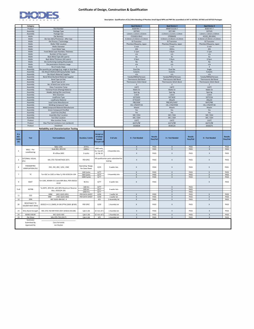
Certificate of Design, Construction & Qualification
Description: Qualification of [Cu] Wire Bonding of Phenitec Small Signal NPN and PNP Die assembled at SAT in SOT563, SOT363 and SOT523 Packages
Category Qual Device 1 Qual Device 2 Qual Device 3
Product Part Number BC847BV‐7 MMDT2222A‐7 BC857AT‐7
Assembly Package Type SOT563 SOT‐363 SOT523
Assembly Package Size 1.6mm x 1.6mm x 0.6mm 2.15mm x 2.1mm x 1.0mm 1.6mm x 1.6mm x 0.8mm
Wafer Die Name(s) C5334S14 Bin2 CP998ADE A5335_856 BIN1
Wafer Die Size (W/L/Thickness) ‐ After Saw 0.33mm x 0.33mm x 0.14mm 0.35mm x 0.35mm x 0.23mm 0.35mm x 0.35mm x 0.23mm
Wafer Die Process / Technology SS Transistor SS Transistor SS Transistor
Wafer Wafer FAB/ Location Phenitec/Okayama, Japan Phenitec/Okayama, Japan Phenitec/Okayama, Japan
Wafer Wafer Diameter 5 inch 5 inch 5 inch
Wafer Front Metal Type AlSi AlSiCu AlSi
Wafer Front Metal Layer Number/ Thickness 2.7µm 2.0µm 2.7µm
Wafer Number of Poly Layers n/a n/a n/a
Wafer Back Metal Type (All Layers) Au Au Au
Wafer Back Metal Thickness (All Layers) 0.9µm 0.9µm 0.9µm
Wafer Die Conforming Coating (Passivation) No No No
Wafer Die passivation thickness range n/a n/a n/a
Wafer No of masks Steps 4 5 4
Assembly Die quantity per package (e.g. single or dual dies) Dual Die Dual Die Single
Assembly Die Attach Method (DB Epoxy/Solder Type) Eutectic Eutectic Eutectic
Assembly Die Attach Material/ Supplier n/a n/a n/a
Assembly Bond Wire/Clip Bond Material/ Supplier Tanaka/NBKQ/Heraues Tanaka/NBKQ/Heraues Tanaka/NBKQ/Heraues
Assembly Bond Type (at Die) Thermosonic Ball Bond Thermosonic Ball Bond Thermosonic Ball Bond
Assembly Bond Type (at LF) Thermosonic Stitich Bond Thermosonic Stitich Bond Thermosonic Stitich Bond
Assembly No. of bond over active area 4 4 2
Assembly Glass Transistion Temp 130°C 130°C 130°CAssembly Terminal Finish (Plating) Material Matte Sn Matte Sn Matte Sn
Assembly Header plating (Die Land Area) Spot Ag Spot Ag Spot Ag
Assembly Wire Diameter 1.0mil 1.0mil 1.0mil
Assembly Leadframe Type SOT563D SOT363E SOT523A
Assembly Leadframe Material EFTEC64T Alloy42 Alloy42
Assembly Lead Frame Manufacturer PBE/ASM PBE/APL/VAST MHT/PBE
Assembly Molding Compound Type CEL‐1702HF9 SK CEL‐1702HF9SK CEL‐1702HF9 SK
Assembly Mold Compound Material Manufacturer Hitachi Hitachi Hitachi
Assembly Green Compound (Yes/No) Yes Yes Yes
Assembly Lead‐Free (Yes/No) Yes Yes Yes
Assembly Assembly Site/ Location SKE / DSH SKE / DSH SKE / DSH
Assembly Test Site/ Location SKE / DSH SKE / DSH SKE / DSH
Product Max Junction Temp 150°C 150°C 150°CProduct Max Thermal resistance Junc (ambient) 833°C/W 625°C/W 833°C/WProduct DataSheet DS30638 DS30125 DS30275
Reliability and Characterization Testing
# in
AEC‐
Q101
(D)
Test Test Conditions Duration / Limits
Accept on
# Failed/
Sample
Size per Lot
# of Lots X = Test NeededResults
Pass/FailX = Test Needed
Results
Pass/FailX = Test Needed
Results
Pass/Fail
Bake 125C 24 Hrs X PASS X PASS X PASSSoak 85C, 85% RH 168Hrs X PASS X PASS X PASS
IR reflow 260C 3 cycles X PASS X PASS X PASS
3EXTERNAL VISUAL
(EV)MIL‐STD‐750 METHOD 2071 PER SPEC X PASS X PASS X PASS
4PARAMETRIC
VERIFICATION (PV)‐55C, 25C, 85C, 125C, 150C
Operating Range,
Per Data Sheet0/25 3 wafer lots X PASS X PASS X PASS
168 Cycles 0/77 X PASS X PASS X PASS
500 Cycles 0/77 X PASS X PASS X PASS1000 Cycles 0/77 X PASS X PASS X PASS
9 HAST Ta=130C, 85%RH 33.3 psia 80% Bias; PER JESD22‐
A11096 Hrs 0/77 3 wafer lots X PASS X PASS
168 Hrs 0/77 X PASS
500 Hrs 0/77 X PASS1000 Hrs 0/77 X PASS
HBM (AEC‐Q101‐001) PER DATA SHEET 0/30 1 wafer lot X PASS X PASS X PASS
MM ( AEC‐Q101‐002) PER DATA SHEET 0/30 1 wafer lot X PASS X PASS X PASS
12 DPA AEC Q101‐004 SEC. 4 0/2 1 Assembly lot X PASS X PASS X PASS
20RESISTANCE TO
SOLDER HEAT (RSH)JESD22 A‐111 (SMD), B‐106 (PTH) (260C @30S) PER SPEC 0/30 1 Assmbly lot X PASS X PASS X PASS
23 Wire Bond Strength MIL‐STD‐750 METHOD 2037 (JESD22‐B116B) Cpk>1.66 0/ min of 5 1 Assmbly lot X PASS X PASS X PASS
24 BOND SHEAR AEC‐Q101‐003 Cpk>1.66 0/ min of 5 1 Assmbly lot X PASS X PASS X PASS
25 Die Shear MIL‐STD‐750 (2017) Cpk>1.66 0/5 1 Assmbly lot X PASS X PASS X PASS
Summary: ____________________________________
Submitted By: Cora Fernando
Approved By: Jon Stocker
Ta=‐65C to 150C or Max Tj, PER JESD22A‐104
Ta=85ºC, 85% RH, with 80% Maximum Reverse
Bias. JESD22A‐101
11
2
7
9 alt
ESD
MSL1 Pre‐
conditioning
TC
H3TRB
All qualification parts submitted for
testing
SMD only,
for Test #7,
8, 9 & 10
3 Assembly lots
3 Assembly lots
3 wafer lots

Certificate of Design, Construction & Qualification
Description: Qualification of C3904S Die shrink assembled at CAT in SOT23 Package
Category Qual Device 1
Product Part Number MMBT3904
Assembly Package Type SOT23
Assembly Package Size 2.9*2.4*1.05mm
Wafer Die Name(s) C3904S
Wafer Die Size (W/L/Thickness) ‐ After Saw 0.26*0.26*0.216mm
Wafer Die Process / Technology BJT / NPN
Wafer Wafer FAB/ Location Kfab / Kansas US
Wafer Wafer Diameter 6 inch
Wafer Front Metal Type AlSiCu
Wafer Front Metal Layer Number/ Thickness 3.5µm
Wafer Number of Poly Layers n/a
Wafer Back Metal Type (All Layers) Au
Wafer Back Metal Thickness (All Layers) 0.5µm
Wafer Die Conforming Coating (Passivation) Ox/Nitride
Wafer Die passivation thickness range 0.75um
Wafer No of masks Steps 5
Assembly Die quantity per package (e.g. single or dual dies) single
Assembly Die Attach Method (DB Epoxy/Solder Type) Eutectic
Assembly Die Attach Material/ Supplier n/a
Assembly Bond Wire/Clip Bond Material/ Supplier Cu
Assembly Bond Type (at Die) Thermosonic Ball Bond
Assembly Bond Type (at LF) Thermosonic Stitch Bond
Assembly No. of bond over active area 2
Assembly Glass Transistion Temp 160°CAssembly Terminal Finish (Plating) Material Leadfree
Assembly Header plating (Die Land Area) n/a
Assembly Wire Diameter 0.8mil
Assembly Leadframe Type SOT‐23A
Assembly Leadframe Material Alloy42
Assembly Lead Frame Manufacturer SLC
Assembly Molding Compound Type GR640HV‐L1
Assembly Mold Compound Material Manufacturer Henkel
Assembly Green Compound (Yes/No) Yes
Assembly Lead‐Free (Yes/No) Yes
Assembly Assembly Site/ Location CAT / Chengdu CH
Assembly Test Site/ Location CAT / Chengdu CH
Product Max Junction Temp 150°CProduct Max Thermal resistance Junc (ambient) 417°C/WProduct DataSheet DS30036
Reliability and Characterization Testing
# in
AEC‐
Q101
(D)
Test Test Conditions Duration / Limits
Accept on #
Failed/
Sample Size
per Lot
# of Lots X = Test NeededResults
Pass/Fail
Bake 125C 24 Hrs X PassSoak 85C, 85% RH 168Hrs X Pass
IR reflow 260C 3 cycles X Pass
3EXTERNAL VISUAL
(EV)MIL‐STD‐750 METHOD 2071 PER SPEC X Pass
4PARAMETRIC
VERIFICATION (PV) ‐55C, 25C, 85C, 125C, 150C
Operating Range,
Per Data Sheet0/25 3 wafer lots X Pass
168 Hrs 0/77 X Pass
500 Hrs 0/77 X Pass1000 Hrs 0/77 X Pass
168 Cycles 0/77 X Pass
500 Cycles 0/77 X Pass1000 Cycles 0/77 X Pass
9 HAST Ta=130C, 85%RH 33.3 psia 80% Bias; PER JESD22‐
A11096 Hrs 0/77 3 wafer lots X Pass
2520 Cycles 0/77 X Pass
7560 Cycles 0/77 X Pass15000 Cycles 0/77 X Pass
HBM (AEC‐Q101‐001) PER DATA SHEET 0/30 1 wafer lot X Pass
MM ( AEC‐Q101‐002) PER DATA SHEET 0/30 1 wafer lot X Pass
12 DPA AEC Q101‐004 SEC. 4 0/2 1 Assembly lot X Pass
20RESISTANCE TO
SOLDER HEAT (RSH)JESD22 A‐111 (SMD), B‐106 (PTH) (260C @30S) PER SPEC 0/30 1 Assembly lot X Pass
23 Wire Bond Strength MIL‐STD‐750 METHOD 2037 (JESD22‐B116B) Cpk>1.66 0/ min of 5 1 Assembly lot X Pass
24 BOND SHEAR AEC‐Q101‐003 Cpk>1.66 0/ min of 5 1 Assembly lot X Pass
25 Die Shear MIL‐STD‐750 (2017) Cpk>1.66 0/5 1 Assembly lot X Pass
Summary: ____________________________________
Submitted By: Adam Knight
Approved By: Jon Stocker
3 Assembly lots
3 wafer lots
All qualification parts submitted for
testing
SMD only,
for Test #7,
8, 9 & 10
3 Assembly lots
3 wafer lots
ESD
MSL1 Pre‐
conditioning
IOL
TC
HTRB
11
2
10
7
5
MIL‐STD‐750 Method 1037 (N/A for TVS)
Ta=‐65C to 150C or Max Tj, PER JESD22A‐104
Ta=150 or Max Tj, Vd/Vr/Vcbo=80%, MIL‐STD‐
750‐1 / PER JESD22 A‐108

Certificate of Design, Construction & Qualification
Description: C2907S die qualification at SAT
Category Qual Device 1 Qual Device 2
Product Part Number MMBT2907A MMST2907A
Assembly Package Type SOT‐23 SOT‐323
Assembly Package Size 2.9 x 1.3 2.0 x 1.25
Wafer Die Name(s) C2907S C2907S
Wafer Die Size (W/L/Thickness) ‐ After Saw 0.35*0.35*0.216mm 0.35*0.35*0.216mm
Wafer Die Process / Technology Bipolar / Small Signal Bipolar / Small Signal
Wafer Wafer FAB/ Location KFAB/Kansas KFAB/Kansas
Wafer Wafer Diameter 150mm 150mm
Wafer Front Metal Type AlSiCu AlSiCu
Wafer Front Metal Layer Number/ Thickness 3.5um 3.5um
Wafer Number of Poly Layers n/a n/a
Wafer Back Metal Type (All Layers) NiV + Au NiV + Au
Wafer Back Metal Thickness (All Layers) 125A NiV + 5150A Au 125A NiV + 5150A Au
Wafer Die Conforming Coating (Passivation) PECVD Oxide/Ntride PECVD Oxide/Ntride
Wafer Die passivation thickness range 15kA Nitride / 6kA Oxide 15kA Nitride / 6kA Oxide
Wafer No of masks Steps 6 6
Assembly Die quantity per package (e.g. single or dual dies) 1 1
Assembly Die Attach Method (DB Epoxy/Solder Type) Eutectic Eutectic
Assembly Die Attach Material/ Supplier n/a n/a
Assembly Bond Wire/Clip Bond Material/ Supplier Cu Cu
Assembly Bond Type (at Die) Thermosonic Thermosonic
Assembly Bond Type (at LF) Thermosonic Thermosonic
Assembly No. of bond over active area 2 2
Assembly Glass Transistion Temp 130 130
Assembly Terminal Finish (Plating) Material Matte Sn Matte Sn
Assembly Header plating (Die Land Area) Spot Ag Spot Ag
Assembly Wire Diameter 1 mil 1 mil
Assembly Leadframe Type SOT‐23A SOT‐323A
Assembly Leadframe Material Alloy42 ACDA194FH
Assembly Lead Frame Manufacturer PBE / VAST / APL PBE / Hitachi
Assembly Molding Compound Type GR640HV‐L1 CEL‐1702HF9SKF
Assembly Mold Compound Material Manufacturer Henkel HITACHI
Assembly Green Compound (Yes/No) yes yes
Assembly Lead‐Free (Yes/No) yes yes
Assembly Assembly Site/ Location SAT/Shanghai SAT/Shanghai
Assembly Test Site/ Location SAT/Shanghai SAT/Shanghai
Product Max Junction Temp 150 150
Product Max Thermal resistance Junc (amibent) 403 °C/W 625 °C/W
Product DataSheet DS30040 DS30081
Reliability and Characterization Testing
# in AEC‐
Q101
(D)
Test Test Conditions Duration / Limits
Accept on #
Failed/
Sample Size
per Lot
# of Lots X = Test NeededResults
Pass/FailX = Test Needed
Results
Pass/Fail
Bake 125C 24 Hrs X PASS X PASSSoak 85C, 85% RH 168Hrs X PASS X PASS
IR reflow 260C 3 cycles X PASS X PASS
3EXTERNAL VISUAL
(EV)MIL‐STD‐750 METHOD 2071 PER SPEC X PASS X PASS
4PARAMETRIC
VERIFICATION (PV)‐55C, 25C, 85C, 125C, 150C
Operating Range,
Per Data Sheet0/25 3 wafer lots X PASS X PASS
168 Hrs 0/77 X PASS X PASS
500 Hrs 0/77 X PASS X PASS1000 Hrs 0/77 X PASS X PASS
168 Cycles 0/77 X PASS X PASS
500 Cycles 0/77 X PASS X PASS1000 Cycles 0/77 X PASS X PASS
9 HAST Ta=130C, 85%RH 33.3 psia 80% Bias; PER JESD22‐
A11096 Hrs 0/77 3 wafer lots X PASS X PASS
2520 Cycles 0/77 X PASS X PASS
7560 Cycles 0/77 X PASS X PASS15000 Cycles 0/77 X PASS X PASS
HBM (AEC‐Q101‐001) PER DATA SHEET 0/30 1 wafer lot X PASS X PASS
MM ( AEC‐Q101‐002) PER DATA SHEET 0/30 1 wafer lot X PASS X PASS
12 DPA AEC Q101‐004 SEC. 4 0/2 1 Assembly lot X PASS X PASS
20RESISTANCE TO
SOLDER HEAT (RSH)JESD22 A‐111 (SMD), B‐106 (PTH) (260C @30S) PER SPEC 0/30 1 Assembly lot X PASS X PASS
23 Wire Bond Strength MIL‐STD‐750 METHOD 2037 (JESD22‐B116B) Cpk>1.66 0/ min of 5 1 Assembly lot X PASS X PASS
24 BOND SHEAR AEC‐Q101‐003 Cpk>1.66 0/ min of 5 1 Assembly lot X PASS X PASS
Summary: ____________________________________
Submitted By: Jon Stocker
Approved By: Paul Whitehead
3 Assembly lots
3 wafer lots
All qualification parts submitted for
testing
SMD only,
for Test #7,
8, 9 & 10
3 Assembly lots
3 wafer lots
ESD
MSL1 Pre‐
conditioning
IOL
TC
HTRB
11
2
10
7
5
MIL‐STD‐750 Method 1037 (N/A for TVS)
Ta=‐65C to 150C or Max Tj, PER JESD22A‐104
Ta=150 or Max Tj, Vd/Vr/Vcbo=80%, MIL‐STD‐
750‐1 / PER JESD22 A‐108
Certificate of Design, Construction & Qualification
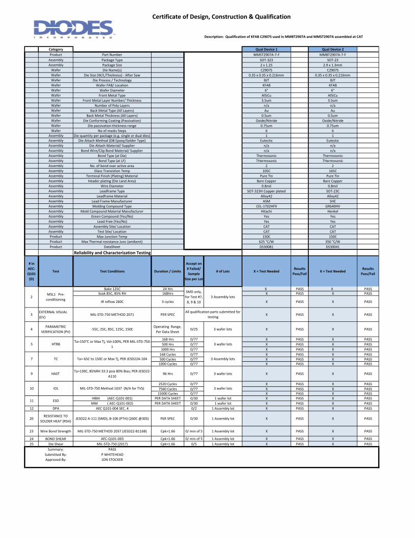
Description: Qualification of KFAB C2907S used in MMBT2907A and MMST2907A assembled at CAT
Category Qual Device 1 Qual Device 2
Product Part Number MMST2907A‐7‐F MMBT2907A‐7‐F
Assembly Package Type SOT‐323 SOT‐23
Assembly Package Size 2 x 1.25 2.9 x 1.3mm
Wafer Die Name(s) C2907S C2907S
Wafer Die Size (W/L/Thickness) ‐ After Saw 0.35 x 0.35 x 0.216mm 0.35 x 0.35 x 0.216mm
Wafer Die Process / Technology BJT BJT
Wafer Wafer FAB/ Location KFAB KFAB
Wafer Wafer Diameter 6" 6"
Wafer Front Metal Type AlSiCu AlSiCu
Wafer Front Metal Layer Number/ Thickness 3.5um 3.5um
Wafer Number of Poly Layers n/a n/a
Wafer Back Metal Type (All Layers) Au Au
Wafer Back Metal Thickness (All Layers) 0.5um 0.5um
Wafer Die Conforming Coating (Passivation) Oxide/Nitride Oxide/Nitride
Wafer Die passivation thickness range 0.75um 0.75um
Wafer No of masks Steps 6 6
Assembly Die quantity per package (e.g. single or dual dies) 1 1
Assembly Die Attach Method (DB Epoxy/Solder Type) Eutectic Eutectic
Assembly Die Attach Material/ Supplier n/a n/a
Assembly Bond Wire/Clip Bond Material/ Supplier n/a n/a
Assembly Bond Type (at Die) Thermosonic Thermosonic
Assembly Bond Type (at LF) THermosonic THermosonic
Assembly No. of bond over active area 2 2
Assembly Glass Transistion Temp 105C 165C
Assembly Terminal Finish (Plating) Material Pure Tin Pure Tin
Assembly Header plating (Die Land Area) Bare Copper Bare Copper
Assembly Wire Diameter 0.8mil 0.8mil
Assembly Leadframe Type SOT‐323H Copper plated SOT‐23C
Assembly Leadframe Material Alloy42 Alloy42
Assembly Lead Frame Manufacturer ASM SHE
Assembly Molding Compound Type CEL‐1702HF9 GR640HV
Assembly Mold Compound Material Manufacturer Hitachi Henkel
Assembly Green Compound (Yes/No) Yes Yes
Assembly Lead‐Free (Yes/No) Yes Yes
Assembly Assembly Site/ Location CAT CAT
Assembly Test Site/ Location CAT CAT
Product Max Junction Temp 150C 150C
Product Max Thermal resistance Junc (amibent) 625 °C/W 350 °C/W
Product DataSheet DS30081 DS30041
Reliability and Characterization Testing
# in
AEC‐
Q101
(D)
Test Test Conditions Duration / Limits
Accept on
# Failed/
Sample
Size per Lot
# of Lots X = Test NeededResults
Pass/FailX = Test Needed
Results
Pass/Fail
Bake 125C 24 Hrs X PASS X PASSSoak 85C, 85% RH 168Hrs X PASS X PASS
IR reflow 260C 3 cycles X PASS X PASS
3EXTERNAL VISUAL
(EV)MIL‐STD‐750 METHOD 2071 PER SPEC X PASS X PASS
4PARAMETRIC
VERIFICATION (PV)‐55C, 25C, 85C, 125C, 150C
Operating Range,
Per Data Sheet0/25 3 wafer lots X PASS X PASS
168 Hrs 0/77 X PASS X PASS
500 Hrs 0/77 X PASS X PASS
1000 Hrs 0/77 X PASS X PASS
168 Cycles 0/77 X PASS X PASS
500 Cycles 0/77 X PASS X PASS1000 Cycles 0/77 X PASS X PASS
9 HAST Ta=130C, 85%RH 33.3 psia 80% Bias; PER JESD22‐
A11096 Hrs 0/77 3 wafer lots X PASS X PASS
2520 Cycles 0/77 X PASS X PASS
7560 Cycles 0/77 X PASS X PASS15000 Cycles 0/77 X PASS X PASS
HBM (AEC‐Q101‐001) PER DATA SHEET 0/30 1 wafer lot X PASS X PASS
MM ( AEC‐Q101‐002) PER DATA SHEET 0/30 1 wafer lot X PASS X PASS
12 DPA AEC Q101‐004 SEC. 4 0/2 1 Assembly lot X PASS X PASS
20RESISTANCE TO
SOLDER HEAT (RSH)JESD22 A‐111 (SMD), B‐106 (PTH) (260C @30S) PER SPEC 0/30 1 Assembly lot X PASS X PASS
23 Wire Bond Strength MIL‐STD‐750 METHOD 2037 (JESD22‐B116B) Cpk>1.66 0/ min of 5 1 Assembly lot X PASS X PASS
24 BOND SHEAR AEC‐Q101‐003 Cpk>1.66 0/ min of 5 1 Assembly lot X PASS X PASS
25 Die Shear MIL‐STD‐750 (2017) Cpk>1.66 0/5 1 Assembly lot X PASS X PASS
Summary: PASS
Submitted By: P WHITEHEAD
Approved By: JON STOCKER
Ta=150 or Max Tj, Vd=100%, PER MIL‐STD‐750‐
1
MIL‐STD‐750 Method 1037 (N/A for TVS)
Ta=‐65C to 150C or Max Tj, PER JESD22A‐104
11
5
2
10
7
ESD
MSL1 Pre‐
conditioning
HTRB
IOL
TC
3 wafer lots
All qualification parts submitted for
testing
SMD only,
for Test #7,
8, 9 & 10
3 Assembly lots
3 Assembly lots
3 wafer lots
Certificate of Design, Construction & Qualification
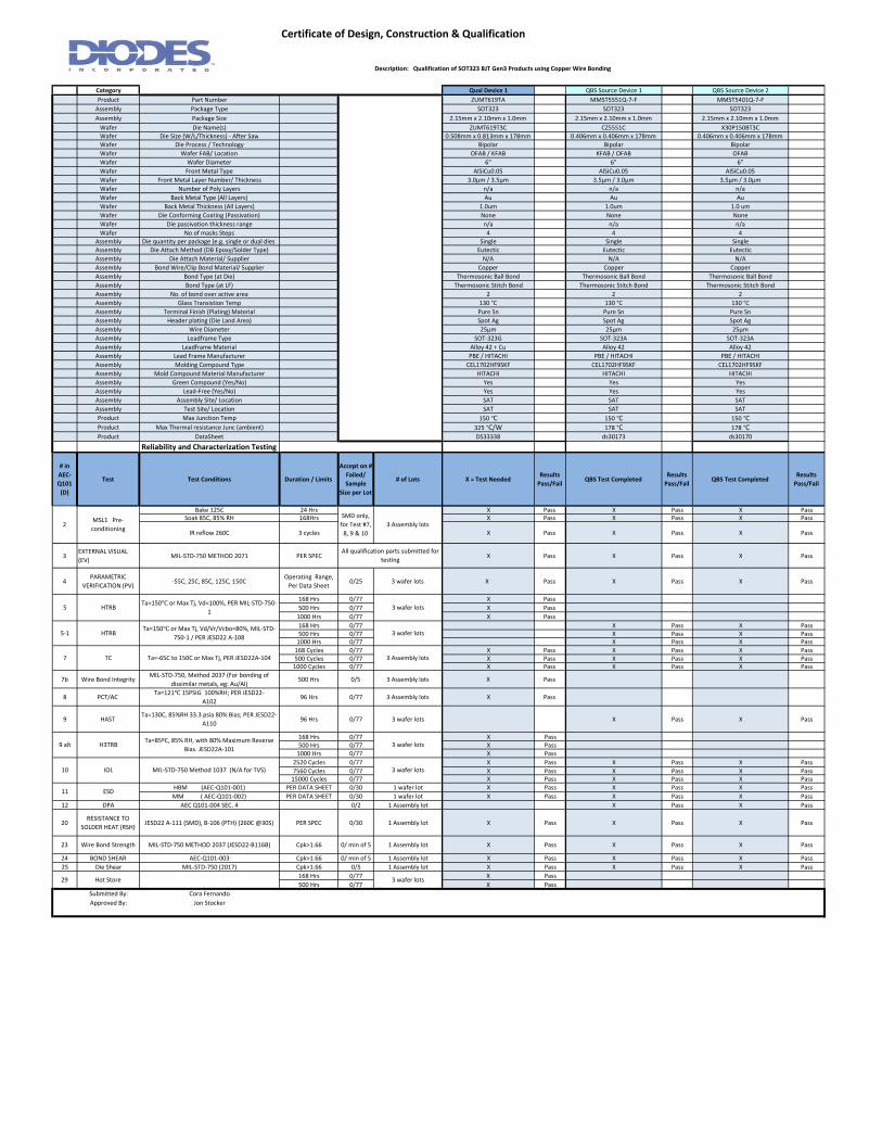
Description: Qualification of SOT323 BJT Gen3 Products using Copper Wire Bonding
Category Qual Device 1 QBS Source Device 1 QBS Source Device 2
Product Part Number ZUMT619TA MMST5551Q‐7‐F MMST5401Q‐7‐F
Assembly Package Type SOT323 SOT323 SOT323
Assembly Package Size 2.15mm x 2.10mm x 1.0mm 2.15mm x 2.10mm x 1.0mm 2.15mm x 2.10mm x 1.0mm
Wafer Die Name(s) ZUMT619T3C CZ5551C X30P150BT3C
Wafer Die Size (W/L/Thickness) ‐ After Saw 0.508mm x 0.813mm x 178mm 0.406mm x 0.406mm x 178mm 0.406mm x 0.406mm x 178mm
Wafer Die Process / Technology Bipolar Bipolar Bipolar
Wafer Wafer FAB/ Location OFAB / KFAB KFAB / OFAB OFAB
Wafer Wafer Diameter 6" 6" 6"
Wafer Front Metal Type AlSiCu0.05 AlSiCu0.05 AlSiCu0.05
Wafer Front Metal Layer Number/ Thickness 3.0µm / 3.5µm 3.5µm / 3.0µm 3.5µm / 3.0µm
Wafer Number of Poly Layers n/a n/a n/a
Wafer Back Metal Type (All Layers) Au Au Au
Wafer Back Metal Thickness (All Layers) 1.0um 1.0um 1.0 um
Wafer Die Conforming Coating (Passivation) None None None
Wafer Die passivation thickness range n/a n/a n/a
Wafer No of masks Steps 4 4 4
Assembly Die quantity per package (e.g. single or dual dies) Single Single Single
Assembly Die Attach Method (DB Epoxy/Solder Type) Eutectic Eutectic Eutectic
Assembly Die Attach Material/ Supplier N/A N/A N/A
Assembly Bond Wire/Clip Bond Material/ Supplier Copper Copper Copper
Assembly Bond Type (at Die) Thermosonic Ball Bond Thermosonic Ball Bond Thermosonic Ball Bond
Assembly Bond Type (at LF) Thermosonic Stitch Bond Thermosonic Stitch Bond Thermosonic Stitch Bond
Assembly No. of bond over active area 2 2 2
Assembly Glass Transistion Temp 130 °C 130 °C 130 °C
Assembly Terminal Finish (Plating) Material Pure Sn Pure Sn Pure Sn
Assembly Header plating (Die Land Area) Spot Ag Spot Ag Spot Ag
Assembly Wire Diameter 25µm 25µm 25µm
Assembly Leadframe Type SOT‐323G SOT‐323A SOT‐323A
Assembly Leadframe Material Alloy 42 + Cu Alloy 42 Alloy 42
Assembly Lead Frame Manufacturer PBE / HITACHI PBE / HITACHI PBE / HITACHI
Assembly Molding Compound Type CEL1702HF9SKF CEL1702HF9SKF CEL1702HF9SKF
Assembly Mold Compound Material Manufacturer HITACHI HITACHI HITACHI
Assembly Green Compound (Yes/No) Yes Yes Yes
Assembly Lead‐Free (Yes/No) Yes Yes Yes
Assembly Assembly Site/ Location SAT SAT SAT
Assembly Test Site/ Location SAT SAT SAT
Product Max Junction Temp 150 °C 150 °C 150 °CProduct Max Thermal resistance Junc (ambient) 325 °C/W 178 °C 178 °CProduct DataSheet DS33338 ds30173 ds30170
Reliability and Characterization Testing
# in
AEC‐
Q101
(D)
Test Test Conditions Duration / Limits
Accept on #
Failed/
Sample
Size per Lot
# of Lots X = Test NeededResults
Pass/FailQBS Test Completed
Results
Pass/FailQBS Test Completed
Results
Pass/Fail
Bake 125C 24 Hrs X Pass X Pass X PassSoak 85C, 85% RH 168Hrs X Pass X Pass X Pass
IR reflow 260C 3 cycles X Pass X Pass X Pass
3EXTERNAL VISUAL
(EV)MIL‐STD‐750 METHOD 2071 PER SPEC X Pass X Pass X Pass
4PARAMETRIC
VERIFICATION (PV)‐55C, 25C, 85C, 125C, 150C
Operating Range,
Per Data Sheet0/25 3 wafer lots X Pass X Pass X Pass
168 Hrs 0/77 X Pass
500 Hrs 0/77 X Pass
1000 Hrs 0/77 X Pass
168 Hrs 0/77 X Pass X Pass500 Hrs 0/77 X Pass X Pass1000 Hrs 0/77 X Pass X Pass
168 Cycles 0/77 X Pass X Pass X Pass500 Cycles 0/77 X Pass X Pass X Pass1000 Cycles 0/77 X Pass X Pass X Pass
7b Wire Bond IntegrityMIL‐STD‐750, Method 2037 (For bonding of
dissimilar metals, eg: Au/Al)500 Hrs 0/5 3 Assembly lots X Pass
8 PCT/AC Ta=121 15PSIG 100%RH; PER JESD22‐
A10296 Hrs 0/77 3 Assembly lots X Pass
9 HAST Ta=130C, 85%RH 33.3 psia 80% Bias; PER JESD22‐
A11096 Hrs 0/77 3 wafer lots X Pass X Pass
168 Hrs 0/77 X Pass500 Hrs 0/77 X Pass1000 Hrs 0/77 X Pass
2520 Cycles 0/77 X Pass X Pass X Pass
7560 Cycles 0/77 X Pass X Pass X Pass15000 Cycles 0/77 X Pass X Pass X Pass
HBM (AEC‐Q101‐001) PER DATA SHEET 0/30 1 wafer lot X Pass X Pass X Pass
MM ( AEC‐Q101‐002) PER DATA SHEET 0/30 1 wafer lot X Pass X Pass X Pass
12 DPA AEC Q101‐004 SEC. 4 0/2 1 Assembly lot X Pass X Pass
20RESISTANCE TO
SOLDER HEAT (RSH)JESD22 A‐111 (SMD), B‐106 (PTH) (260C @30S) PER SPEC 0/30 1 Assembly lot X Pass X Pass X Pass
23 Wire Bond Strength MIL‐STD‐750 METHOD 2037 (JESD22‐B116B) Cpk>1.66 0/ min of 5 1 Assembly lot X Pass X Pass X Pass
24 BOND SHEAR AEC‐Q101‐003 Cpk>1.66 0/ min of 5 1 Assembly lot X Pass X Pass X Pass
25 Die Shear MIL‐STD‐750 (2017) Cpk>1.66 0/5 1 Assembly lot X Pass X Pass X Pass
168 Hrs 0/77 X Pass
500 Hrs 0/77 X Pass
Submitted By: Cora Fernando
Approved By: Jon Stocker
3 Assembly lots
3 wafer lots
3 wafer lots
3 wafer lots
All qualification parts submitted for
testing
SMD only,
for Test #7,
8, 9 & 10
3 Assembly lots
3 wafer lots
ESD
MSL1 Pre‐
conditioning
HTRB
IOL
TC
H3TRB
HTRB
2
10
7
9 alt
5‐1
3 wafer lots29 Hot Store
Ta=150 or Max Tj, Vd=100%, PER MIL‐STD‐750‐
1
MIL‐STD‐750 Method 1037 (N/A for TVS)
Ta=‐65C to 150C or Max Tj, PER JESD22A‐104
Ta=85ºC, 85% RH, with 80% Maximum Reverse
Bias. JESD22A‐101
Ta=150 or Max Tj, Vd/Vr/Vcbo=80%, MIL‐STD‐
750‐1 / PER JESD22 A‐108
11
5

CERTIFICATE OF DESIGN AND CONSTRUCTION
Diodes Form No. DW-009_R3.doc Page 1 of 1 Rel Date: 5 Dec 07 Diodes Incorporated www.diodes.com Print Date: 2/19/16 3:19 PM
Assembly and Test Site
DIODES INC Glass transition temperature (TG)
110℃
DIC P/N DLP05LC-7 Lead material type SOT-23A
Package Type SOT-23 Lead Material manufacturer MHT/PBE/VAST/NBKQ
DIE P/N RGP6V0G+B1001FM*2 Lead plating/ coating Pb free
Die line or process ARR Lead frame material type Alloy42
Wafer Diameter 5" Header plating (Die land area) Spot Ag
Wafer Fab Site(s) Phenitec+KFAB Max junction temperature(Tj) 125℃
ID method (multiple sites)
NA Max thermal resistance junction to case (θJC)
NA
Assembly Locations(s)
DIODES INC. IN SHANGHAI, Plant1,NO.111-10 Songjiang Export Processing Zone, Shanghai,P.R.China 201600
Max thermal resistance junction to ambient (θJA)*
NA
Test Locations(s) DIODES INC. IN SHANGHAI, Plant1,NO.111-10 Songjiang Export Processing Zone, Shanghai,P.R.China 201600
Front metal type (Top layer) AlSiCu
Die attach Method / Material
EUTECTIC Front metal thickness (Top layer)
RGP6V0G - 2.5um
B1001FM - 3.5um
Bond wire material & dia.
Cu wire,1.3mil Back metal type (All layers) RGP6V0G - Au
B1001FM - 125A NiV + 5150A Au
Bond type (at top side of the die)
Thermo sonic Back metal thickness (all Layers)
RGP6V0G - 0.9um
B1001FM - 125A NiV + 5150A Au
Bond type (at leadframe)
Thermo sonic Die conforming coating NA
No. of bonds over active area
3 Die size (width x length x thickness) in mm
RGP6V0G - 0.44*0.44*0.18mm
B1001FM - 0.28*0.28*0.216mm
Package material type
GR640HV-L1 Die passivation thickness range NA
Package material manufacturer
HENKEL No. of mask steps N/A
*Show conditions (i.e. pad size, board material, copper thickness, etc. Attachments: Requirements:
1) Die Photo A separate Certificate of Design, Construction and Qualification shall be submitted for each P/N and assembly location.
2) Package outline drawing Document shall be signed by a responsible individual at the supplier who can verify that all of the above information is correct. Type name and sign.
3) Die cross-section drawing 4) Wire bond & die placement diagram 5) Test circuits, bias levels and conditions
Completed by Date Certified by Date
Typed/Printed Jenny Liu February 24, 2014
Liang Gao 2014-2-24
Signature
Title

FACTORY: PART NUMBER: DLP05LC SWR1401234 Customer
Package:SOT23
DW-008 (AEC Q101) Test#
Test Description Test Conditions #Lots #To Test Results REMARKS
7.3.2 (1)PRE- AND POST- STRESS ELECTRICAL TEST (TEST)
Per Spec N/A
7.3.3 (2) PRECONDITIONING (PC) JSED22 A-113 N/A for Axial 1 308 0/308
7.3.5.1 (3) EXTERNAL VISUAL (EV) MIL-STD-750 METHOD 2071 1 500 0/500
7.3.5.2 (4) PARAMETRIC VERIFICATION (PV) 1 of 3 25 0/25
Lot #2 2 of 3 25
Lot #3 3 of 3 25
7.3.5.3 FORWARD SURGE MIL-750D, Method 4066 1 45
7.3.5.4 (5) HIGH TEMP. REVERSE BIAS (HTRB) T=150*C/Vr=5v,PER JESD22 A-108 1 77
Pretest 1 77 0/77
@ 168 Hours T=150*C/Vr=5v,PER JESD22 A-108 1 77 0/77
@ 500 Hours T=150*C/Vr=5v,PER JESD22 A-108 1 77 0/77
Final 1000Hours T=150*C/Vr=5v,PER JESD22 A-108 1 77 0/77
(6) HIGH TEMP GATE BIAS (HTGB) MIL-750D, Method 4066 N/A N/A N/A
7.3.5.5 (7) TEMPERATURE CYCLING (TC) T=-65*C-150*C, PER JESD22 A-104
Pretest 1 77 0/77
@ 168Cycles T=-65*C-150*C, PER JESD22 A-104 1 77 0/77
@ 500Cycles T=-65*C-150*C, PER JESD22 A-104 1 77 0/77
@ 1000Cycles T=-65*C-150*C, PER JESD22 A-104 1 77 0/77
7.3.5.6 (8) AUTOCLAVE (AC) T=121*C 15PSIG 100%RH 1 77 0/77 96h
7.3.5.7 (9) H3TRB T=85℃ RH=85% Vg=80% 1 77Not required if HAST passed
Pretest 1 77
@ 500 Hours T=85℃ RH=85% Vg=80% 1 77
Final 1000 Hours T=85℃ RH=85% Vg=80% 1 77
7.3.5.7 (9a)HIGHLY ACCELERATED STRESS TEST (HAST)
T=130℃ RH=85% Vr=80% of BVR 1 77 0/77 96hrs
7.3.5.8 (10) INTERMITTENTOPERATING LIFE (IOL) If=100mA, PER MIL-STD-750 METHOD 103715000Cycles @
2min on/off
Pretest MIL-STD-750 METHOD 1037 1 77
After 15000cy MIL-STD-750 METHOD 1037 1 77(10a) POWER AND TEMP. CYCLE (PTC) JESD22 A-105, Per Table AEC-Q101, p11 1 77
(Optional) Pretest JESD22 A-105, Per Table AEC-Q101, p11 1 77 Midpoint JESD22 A-105, Per Table AEC-Q101, p11 1 77
After JESD22 A-105, Per Table AEC-Q101, p11 1 77
7.3.5.9 (11) ESD CHARACTERIZATION (ESD) PER AEC-Q101-001 & -002 1 60 0/60MM 400VHBM 8kV
7.3.5.10 (12) D.P.A. (DPA) AEC Q101-004 SEC. 4 1 2 0/27.3.5.11 (13) PHYSICAL DIMENSION (PD) PER JESD22 B-100 1 30 0/30
7.3.5.12 (14) TERMINAL STRENGTH (TS) MIL-STD-750, Method 2036 1 30 N/A
7.3.5.12 (14) TERMINAL STRENGTH (TS) MIL-STD-750, Method 2036 N/A N/A N/A7.3.5.13 (15) RESISTANCE TO SOLVENTS (RTS) JESD22 B-107 N/A N/A N/A
(16) CONSTANT ACCELERATION (CA) N/A, not hermetically sealed device. N/A N/A N/A
7.3.5.14 (20) RESISTANCE TO SOLDER HEAT (RSH) JESD22 B-106 1 30 0/30 260*C @30S
7.3.5.16 (22) THERMAL RESISTANCE (TR) JESD 24-3, 24-4, 24-6 as appropriate 1 10 0/10 408*C/W
7.3.5.18 (24) BOND SHEAR (BS) AEC-Q101-003 1 30 0/30
7.3.5.19 (25) DIE SHEAR (DS) MIL-STD-750 METHOD 2017 1 30 0/30
(26) UNCLAMPED INDUCTIVE SWITCHING (UI N/A, not for Diode N/A N/A N/A
(27) DIELECTRIC INTEGRITY (DI) N/A, not for Diode N/A N/A N/A
Summary:
Approved by:Adam Gu 04/29/14
Q-Form Q014-4,Rev.K
Reliability Test Summary Report
SHANGHAI KAIHONG ELECTRONIC CO.,LTD
DIODES INC.:
LABORATORY (If Different):PART DESCRIPTION:2nd wafer source QUAL (RGP6V0G+B1001FM,GR640HV-L1,1.3Cu)
N/A
Per Data Sheet Characteristic VZ@IZT=1mACharacteristic IR@VR=5VTa1=-55*C, Ta2=25*C, Ta3=85*C, Ta4=150*C
The lot passed pre-con and 1000hrs full hirel test.
Submitted by: Joan Yu 04/29/14