Dinesh P R Thanu, Platform Lead ... - Ceramics Expo … · Ceramics Expo, Apr 26' 2017, OH....
11
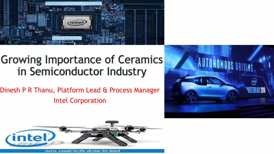
Dinesh P R Thanu, Platform Lead & Process Manager Intel Corporation
Transcript of Dinesh P R Thanu, Platform Lead ... - Ceramics Expo … · Ceramics Expo, Apr 26' 2017, OH....
Dinesh P R Thanu, Platform Lead & Process Manager
Intel Corporation
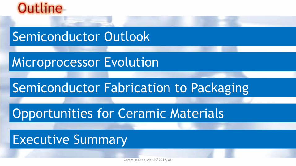
Microprocessor Evolution
Semiconductor Outlook
Semiconductor Fabrication to Packaging
Opportunities for Ceramic Materials
Executive Summary
Ceramics Expo, Apr 26' 2017, OH

• Continuous growth market
• Moore’s law extends to make faster,
smaller and energy efficient packages
• Mobile, Automotive and Artificial
Intelligence segment continues to flourish
• IoT brings in a connected world
• Advanced fabrication and packaging
requisite raises
• Economy of silicon manufacturing
and packaging R&D becoming
challenging
• Performance and cost driving
technological development
• High competition and mounting need
for novel designs and materialsCeramics Expo, Apr 26' 2017, OH
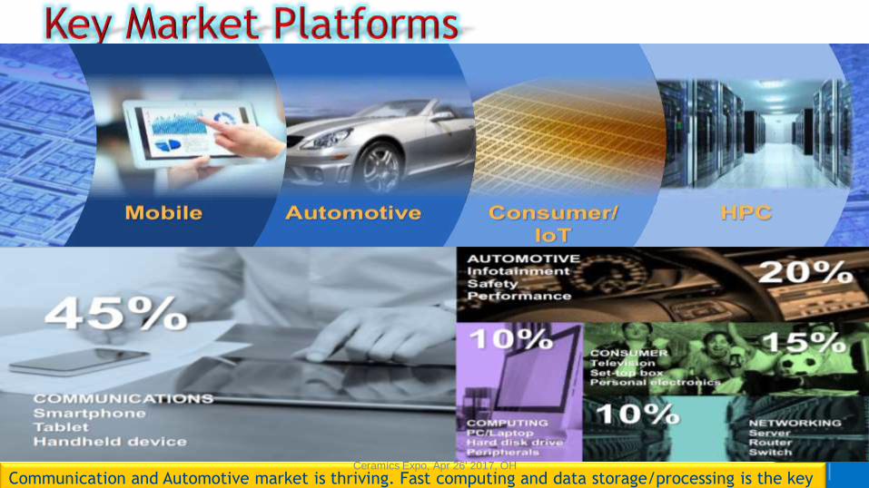
Communication and Automotive market is thriving. Fast computing and data storage/processing is the keyCeramics Expo, Apr 26' 2017, OH
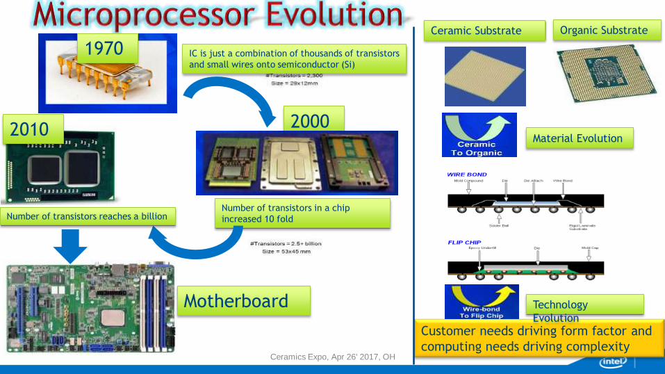
1970
20002010
Organic Substrate
Customer needs driving form factor and
computing needs driving complexity
Motherboard
IC is just a combination of thousands of transistors
and small wires onto semiconductor (Si)
Number of transistors in a chip
increased 10 foldNumber of transistors reaches a billion
Ceramic Substrate
Material Evolution
Technology
Evolution
Ceramics Expo, Apr 26' 2017, OH

• The power requirements are
increasing but the Si size is getting
smaller
• Getting the power in and dissipating
the heat out are two major
challenges
• There is need to optimize complete
Si package integrated power delivery
solution
• There is also corresponding need to
reduce the system heat with
efficient package designs and
materials
Ceramics Expo, Apr 26' 2017, OH

An unprocessed Si wafer costs a
few hundred bucks but is worth
in millions after assembly
Automotive and AI products
have multiple chips on one
package. ROI, reliability and
data processing are huge
challenges
For Si fabrication all fabs need to
be identical to make a robust,
reliable part
Maintenance of each fab costs
billions
It takes a few years to
make a new technology
part but less years to
obsolete them
Fabrication process involves
hundreds of cleaning, etching
and processing steps
Ceramics Expo, Apr 26' 2017, OH
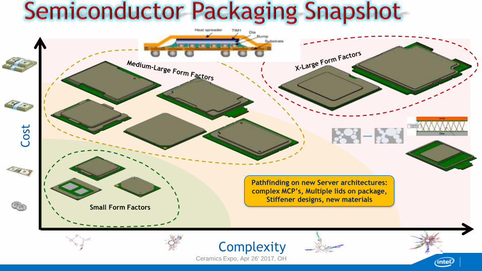
Complexity
Cost
Apple River:Small Form Factors
Pathfinding on new Server architectures:
complex MCP’s, Multiple lids on package,
Stiffener designs, new materials
Ceramics Expo, Apr 26' 2017, OH
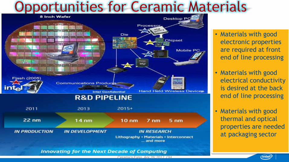
• Materials with good
electronic properties
are required at front
end of line processing
• Materials with good
electrical conductivity
is desired at the back
end of line processing
• Materials with good
thermal and optical
properties are needed
at packaging sector
Ceramics Expo, Apr 26' 2017, OH
Semiconductor evolution, its applications as well as fabrication and
packaging challenges are reviewed
Microelectronic packaging applications are growing rapidly in the past
decade. Performance, Integration and Reliability are the key drivers
IoT, data storage and processing demands will drive this growth further
Innovative technology, smart designs and novel materials are absolutely
required in the future
Ceramic materials with good electronic and/or electrical and/or thermal
properties with cost benefit will serve to address some of the current
fabrication and packaging process challenges
Ceramics Expo, Apr 26' 2017, OH

Intel Corporation | Dinesh Thanu | Email: [email protected] | Mobile: 5738236428
Ceramics Expo, Apr 26' 2017, OH