Dimming Power LED Using a SEPIC Converter and MCP1631 PIC...
22
© 2009 Microchip Technology Inc. DS01261A-page 1 AN1261 INTRODUCTION This application note covers the general concept, design and some source code modifications for using the MCP1631HV Digitally Controlled Programmable Current Source Reference Design for an LED lighting application. The document offers additional insight into the MCP1631HV Digitally Controlled Programmable Current Source Reference Design. A Microchip MCP1631 PWM controller and a low-cost PIC16F616 microcontroller are used to manage a SEPIC (Single Ended Primary Inductive Converter) powertrain. The SEPIC topology is then used to drive and dim Light Emitting Diodes (LEDs). The LED technology continues to change and evolve. The energy efficiency (lumens/watt) of today’s LEDs allows them to replace the classical tungsten filament and gas vapor lighting systems with solid-state technology. The most efficient LEDs are able to perform as well as Compact Fluorescent Lamps (CFL). The most important advantage of LEDs over tungsten and gas vapor bulbs is the cycle life. LED lifetimes currently show a 30% improvement over their counterparts. LEDs are being used in the automotive and commercial lighting industries with good results. LEDs must be carefully integrated into lighting systems because of their sensitivity to thermal and electrical stress. The LED current must be optimized for both thermal and electrical characteristics. Excessive driving current will deteriorate LED performance, shorten the lifetime, and cause permanent reduction in the luminous intensity. LEDs may be driven using constant current sources in order to maintain a consistent color output. One low cost but inefficient solution for driving LEDs is using series resistors. The series resistor method is very sensitive to power supply variation. Constant LED current depends on a constant supply voltage. Any variation of the voltage supplying the resistor and LED combination will result in a change in current and thus a change in output color. There are more efficient solutions for driving LEDs that save energy and provide good current control. Two methods of driving an LED are Constant Current and Pulse Width Modulation (PWM) current control. The PWM driver is used to dim an LED and is based upon the persistence of vision of the human eye. The current does not flow through the LED continuously. The PWM period is normally in the range of 100 Hz to 250 Hz. Dimming is obtained by changing the PWM duty cycle. Variations in supply voltage will directly affect the LED current. The Constant Current Source driver is used to supply the LED with a constant current. The constant current results in a consistent LED color output. A high frequency PWM signal may be used to control the current that is flowing through the LED. The PWM signal is used to set the LED current and thus the LED intensity. The Constant Current Source driver is based upon driving the LED with a constant current source to obtain the desired brightness and color. The current source is controlled by a high frequency PWM signal. The PWM modulated constant current source is set to the desired LED current. By changing the PWM duty cycle, the LED current can be adjusted for desired intensity and to offset aging. Constant current driving is recommended to eliminate light flickering and electrical stress due to voltage fluctuations. An important observation is the LED is not affected by the variation of input power supply voltage that can vary as much as +/- 30% of the nominal value. The design topology used for this application note will be the Single Ended Primary Inductive Controller or SEPIC topology. The SEPIC topology allows both buck and boost operation. This allows for a constant current drive output with variations in input voltage. The SEPIC uses a current sense feedback loop for efficient control. Microchip’s MCP1631HV Digitally Controlled Program- mable Current Source Reference Design is used for this application note. Author: Valentin C. Constantin Microchip Technology Inc. Dimming Power LEDs Using a SEPIC Converter and MCP1631 PIC Attach PWM Controller
Transcript of Dimming Power LED Using a SEPIC Converter and MCP1631 PIC...

AN1261Dimming Power LEDs Using a SEPIC Converter and
MCP1631 PIC Attach PWM Controller
INTRODUCTIONThis application note covers the general concept,design and some source code modifications for usingthe MCP1631HV Digitally Controlled ProgrammableCurrent Source Reference Design for an LED lightingapplication. The document offers additional insight intothe MCP1631HV Digitally Controlled ProgrammableCurrent Source Reference Design. A MicrochipMCP1631 PWM controller and a low-cost PIC16F616microcontroller are used to manage a SEPIC (SingleEnded Primary Inductive Converter) powertrain. TheSEPIC topology is then used to drive and dim LightEmitting Diodes (LEDs).
The LED technology continues to change and evolve.The energy efficiency (lumens/watt) of today’s LEDsallows them to replace the classical tungsten filamentand gas vapor lighting systems with solid-statetechnology. The most efficient LEDs are able toperform as well as Compact Fluorescent Lamps (CFL).The most important advantage of LEDs over tungstenand gas vapor bulbs is the cycle life. LED lifetimescurrently show a 30% improvement over theircounterparts. LEDs are being used in the automotiveand commercial lighting industries with good results.
LEDs must be carefully integrated into lighting systemsbecause of their sensitivity to thermal and electricalstress. The LED current must be optimized for boththermal and electrical characteristics. Excessivedriving current will deteriorate LED performance,shorten the lifetime, and cause permanent reduction inthe luminous intensity.
LEDs may be driven using constant current sources inorder to maintain a consistent color output. One lowcost but inefficient solution for driving LEDs is usingseries resistors. The series resistor method is verysensitive to power supply variation. Constant LEDcurrent depends on a constant supply voltage. Anyvariation of the voltage supplying the resistor and LEDcombination will result in a change in current and thusa change in output color. There are more efficientsolutions for driving LEDs that save energy and providegood current control. Two methods of driving an LEDare Constant Current and Pulse Width Modulation(PWM) current control.
The PWM driver is used to dim an LED and is basedupon the persistence of vision of the human eye. Thecurrent does not flow through the LED continuously.The PWM period is normally in the range of 100 Hz to250 Hz. Dimming is obtained by changing the PWMduty cycle. Variations in supply voltage will directlyaffect the LED current.
The Constant Current Source driver is used to supplythe LED with a constant current. The constant currentresults in a consistent LED color output. A highfrequency PWM signal may be used to control thecurrent that is flowing through the LED. The PWMsignal is used to set the LED current and thus the LEDintensity.
The Constant Current Source driver is based upondriving the LED with a constant current source to obtainthe desired brightness and color. The current source iscontrolled by a high frequency PWM signal. The PWMmodulated constant current source is set to the desiredLED current. By changing the PWM duty cycle, theLED current can be adjusted for desired intensity andto offset aging.
Constant current driving is recommended to eliminatelight flickering and electrical stress due to voltagefluctuations. An important observation is the LED is notaffected by the variation of input power supply voltagethat can vary as much as +/- 30% of the nominal value.
The design topology used for this application note willbe the Single Ended Primary Inductive Controller orSEPIC topology. The SEPIC topology allows both buckand boost operation. This allows for a constant currentdrive output with variations in input voltage. The SEPICuses a current sense feedback loop for efficient control.Microchip’s MCP1631HV Digitally Controlled Program-mable Current Source Reference Design is used forthis application note.
Author: Valentin C. Constantin Microchip Technology Inc.
© 2009 Microchip Technology Inc. DS01261A-page 1

AN1261
LED BACKGROUNDThere are a few important parameters that must beconsidered when designing an LED driver.
LED Power, Maximum Forward Current and VoltageGenerally, the LED manufacturers recommend drivingLEDs at constant current. For power type LEDs, thedrive current covers hundreds of milliamps. Standardvalues which are currently used for LED drive currentare: 350 mA, 700 mA, 1A and higher. Some standardpower LEDs are rated for 1W, 3W, and 5W. LED Poweris Vf x If, where Vf is the forward voltage of the LED andIf is the forward current.
Power LED applications utilizing higher current levelswaste energy and create excessive heat when suppliedby series resistors. Any power supply voltage variationwill result in a change in LED current and luminousintensity. It is important to note that the LED’s forwardvoltage varies from device to device and also variessignificantly with temperature.
FIGURE 1: Typical Forward Current vs. Forward Voltage for a White, Blue, Green, and Amber Power LEDs (P3 series) at +25°C.
The Direct Relation between Forward Voltage and the Color of the LED, Maximum Reverse VoltageDifferent color LEDs have different forward voltage (Vf)drops based upon the diode chemistry. A red LEDdissipates less energy than a white LED whenoperated at the same current level. That is because thered LED has a lower Forward Voltage drop than thewhite LED. LED manufacturers datasheets will providethe maximum forward voltage drop (Vfmax) at a givenmaximum forward current (Ifmax). The higher Vfmaxvalues are typically for white and blue LEDs and thelower are typically for red LEDs.
The typical forward voltage drop of a red LED (ultra red,super red, or amber) ranges from 1.8V to 2.2V. Yellowand green LEDs range from 2.1V to 2.2V. Blue andwhite (cool or warm) LEDs range from 3.6V to 3.8V.The user should consult the manufacturers data sheetfor the proper design parameters when using highpower LEDs.
Another important parameter is the Maximum ReverseVoltage (Vrmax), which is typically 5V. Applying reversevoltage in excess of the manufacturersrecommendation will degrade the LED and maydestroy it.
Series and Parallel ConnectionIf the user intends to connect two or more power LEDsin series, it is necessary to calculate the sum of theindividual forward voltages. The color of the LEDs usedmay be different when using a series topology.
FIGURE 2: Topology of an LED String (Series and Parallel Connection).The LED string can be driven by a Constant Currentdriver without series resistors. The sum of the forwardvoltage of each diode in a series string must not exceedthe maximum voltage capability of the current source.
Due to LED tolerances, parallel connections using asingle current sense may not be able to maintain auniform intensity and color. Better control is done usingseparate current sensing for each LED rung in aparallel system.
The advantage of paralleling LEDs is that more LEDscan be supplied at lower output voltage levels onconstant current supplies. If slight variations inluminous intensity are tolerable, a single current sensecan be used to control the current loop. However, if onerung of the parallel LED string fails, the current throughthe other LEDs will increase and possibly causeundesirable consequences. Therefore, it isrecommended to monitor current through each rungand drive each rung as if the string was a series string.
0
50
100
150
200
250
300
350
400
0 0.5 1 1.5 2 2.5 3 3.5 4Forward Voltage (V)
Forw
ard
Cur
rent
(mA
) White & BlueGreenAmber
DS01261A-page 2 © 2009 Microchip Technology Inc.

AN1261
When LEDs are connected in series, the maximumreverse voltage increases with each additional LEDadded to the string. The group of LEDs may make up aseries connected system or they may make up onerung of a parallel connected system.Operating Temperature and Cooling the Power LEDThe forward voltage of an LED is temperaturedependent. The temperature coefficient of forwardvoltage is published in the data sheet and its value isaround 3 to 5 mV/°K, depending on the LED’s color.This parameter shows the changes in forward voltagewith the ambient temperature. The temperatureincreases directly with forward current. The OperatingTemperature Range is generally between -20°C and+85°C. It is important to keep the LED case tempera-ture around 30°C to 40°C for good results. The LEDjunction can typically work at a maximum of +125°C.
The LED manufacturers recommend in theirdatasheets that a heatsink be used with the powerLEDs. A successful design starts with the transfer ofLED heat away from the device. Two typical methodsused to provide proper heat sinking are an externalheatsink or the printed circuit board (PCB) layout.
A PCB on FR4 substrate with a large copper area andthermal vias under a surface mount (SMD) LED is alow-cost but inefficient solution. For good thermalresults, the PCB needs to be double-sided. PCBheat-sinking is not indicated for power LEDs thatrequire more than 1W. Modern lighting lamps use MetalCore PCBs (MCPCB) with special substrates likealuminum or copper. Copper offers the best thermalconductivity. These PCBs offer better cooling becauseof the lower thermal resistance of the core metalcompared to FR4 fiberglass. The heat is dissipated inall directions on the metal surface. Where the spacedoes not permit a large heat sink or a large metal PCB,a small electric fan may be used to force the air acrossthe heat sink.
It is recommended to use extra thermal protectiondevices to avoid accidental overheating due to wrongdrive current, high ambient temperature or fan fault.The extra protection can be managed by an electroniccontroller. A small NTC thermistor or a semiconductorsensor may be placed on the LED heat sink or on themetal PCB. The temperature trip point may be setaround 30°C to 40°C.
Note that the short term effect of excessive heating iscolor shifting, which is reversible. The long term effectof excessive heating is a permanent decrease inluminous intensity and LED life cycle. The idealoperating temperature is typically 25°C. The luminousintensity will be at a maximum around this temperature.
The red and amber LEDs are affected the most byheating. The white LED is least affected by heating.
Minimum Heat Sink Requirements, Thermal ModelingWhen designing a lighting system with power LEDs, abig challenge is thermal management. Thermalmanagement includes the selection of the coolingmethod or combination of methods. Thermalmanagement methods may consist of PCB material,fan, and heat sinks and their respective fasteningprocesses. After selecting the cooling method, thecooling system may then be designed.
Thermal modeling is used to predict the junctiontemperature of the LED in order to avoid exceeding theLED thermal limits specified in the datasheet. Thethermal limit for power LEDs is typically between+120°C and +135°C.
The thermal model used in thermal managementdesign is the concept of Thermal Resistance (Rt), givenin °C/W. Thermal resistance is defined as the ratio oftemperature difference to the corresponding electricalpower dissipation.
EQUATION 1:
EQUATION 2:
EQUATION 3:
LED manufacturers typically specify in their datasheets the thermal resistance from the diode junction tothe ambient RtJA (solder point or LED case).
Thermal resistances RtJC (Thermal Resistance fromjunction to case) and RtCA (Thermal Resistance fromcase to air) should be optimized for each application.
RtJA C W⁄o[ ] TJA P⁄ dLEDΔ=
Where:
RtJA = represents the thermal resis-tance from junction to ambient.
PdLED = the electrical power dissipated by LED.
ΔTJA = the difference between junction and ambient temperatures.
PdLED W[ ] Vf If×=
Where:
Vf = the forward voltage.If = the forward current.
TJA Co[ ]Δ TJ TA–=
Where:
TJ = the junction temperature.TA = the ambient temperature.
© 2009 Microchip Technology Inc. DS01261A-page 3

AN1261
Since RtJC is determined by the device construction,only RtCA may be optimized for thermal efficiency. RtJCtypically ranges from 3°C/W to 4°C/W, depending onthe LED manufacturer. Increasing the heat sink surfacearea will improve the heat dissipation.The typical thermal model of an LED package consistsof:
• LED power dissipation (Equation 2) which is modeled as a current source
• thermal resistance which is modeled as a resistor (Equation 1)
• the difference between ambient temperature and junction temperature which is modeled as a voltage source (Equation 3)
These are solved by Ohm's law following the model inFigure 3. The working junction temperature, TJ, mustbe kept lower than the TJmax of the LED.
FIGURE 3: Typical Thermal Model of an LED.RtJA is a sum of RtJC and RtCA (Equation 4). RtCA is thesum of the case-to-sink thermal resistance (RtCS) andthe sink-to-air thermal resistance (RtSA).Substituting for RtCA and solving Equation 1, we obtainthe minimum RtSA heat sink requirement for theapplication (Equation 4). There are manufacturers thatoffer spreadsheets with several heat sink models andtheir RtSAvalues. References for a few power LEDmanufacturers are listed in the References section [9;10]. The manufacturers web sites offer additionalinformation about thermal management.
EQUATION 4:
Mounting a power LED ensemble on a heat sink mayrequire a thermal adhesive such as tape or thermalgrease. Thermal adhesive tape is recommended forwide and flat surfaces. Avoid any air pockets betweenthe thermal adhesive and the attached face whenapplying the tape.
There is a dependence between the working junctiontemperature and the PCB or heat sink thickness.Thicker metal provides a lower working junctiontemperature. This dependence on thickness can beseen in Figure 4 for a typical 1W P3 series LED.
FIGURE 4: Base Thickness Dependence of Temperature for Power LEDs.
Luminous Intensity. Viewing AngleThe unit of measurement commonly used to describethe LED intensity is the millicandela (mcd).
1000 mcd = 1 candela.
Part of the SI system of measurement, one candela(cd) is the monochromatic radiation of 540 × 1012 Hzwhich has a radiant intensity of 1/683 Watt persteradian in the same direction. The unit ofmeasurement commonly used for most other lightsources is the Lumen. Lumens are units of LuminousFlux. The Luminous Flux (lumens) from a light sourceis equal to the Luminous Intensity (candelas) multipliedby the solid angle over which the light is emitted.
The solid angle is the angle (here defined in 3D space)that an object subtends at a point. It is a measure ofhow big an object appears to an observer who islooking from that object. The Lumens measure howmuch light actually falls on a surface.
Two optical parameters that are very important whenwe choose a power LED for a lighting application arethe luminous intensity and the viewing angle. It maytake some extra calculations to determine whichmanufacturer’s power LED is right for your application,as each manufacturer tends to test their LEDs underdifferent operating conditions. For lighting applications,an LED with a 100° to 130° viewing angle is typicallyrecommended. Lumens per watt (lm/W) is a measureof efficiency in converting electrical energy to light.Multiply this by the watts dissipated in the LED to getlumens.
RtJA
ΔTJA
Pd = Vf X If
RtJA C W⁄o[ ] RtJC RtCA+=
RtJA C W⁄o[ ] RtJC RtCS RtSA+ +=
2526272829303132333435
1 2 3 4 5 6 7 8Base Thickness (mm)
Tem
pera
ture
(°C
)
Heat SinkMetal PCBChip
DS01261A-page 4 © 2009 Microchip Technology Inc.
AN1261
POWER LED DIMMING SOLUTIONSThere are applications that have the requirement tocontrol the luminous intensity of LEDs. The modalitiesfor adjusting the brightness of LEDs were summarizedin the previous section:
• Adjusting the forward current value• Dimming by Pulse-Width-Modulation (PWM)
Adjusting the Forward Current ValueGenerally, there are two methods to drive power LEDsby constant current. One method is to use a constantcurrent source and the other method is to use constantvoltage source. The constant current source methodcan drive the LED with a programmed current at theexpense of a few more circuit devices. Dimming isobtained by modifying the value of current supplied bythe current source.
The constant voltage source method is simplyconnecting the LED to the constant voltage powersupply in series with a resistor chosen for the desiredcurrent. It is the simplest and lowest-cost solution andthus a popular way to drive LEDs when efficiency andcolor range are not critical. Dimming would requireeither stepping the input voltage or switching differentresistor taps to obtain a new current through the LED.
From an efficiency and performance standpoint, thebest choice is a current source that has the ability togenerate digitally programmable current levels asneeded. A digitally programmable current source mayuse a current sense resistor in the control loop tomonitor the LED current. The current sense would beused by the control loop to maintain regulation aboutthe programmed current setpoint. The current senseresistor is part of the output loop in a SEPIC topologysetup. The resistor senses the loop current of theSEPIC topology consisting of the secondary coil,rectifier and LED. The loop current of the SEPICtopology consisting of the primary coil, switch andsource power supply is sensed by a separate resistor.The primary sense monitors peak current in the primaryloop. The secondary sense monitors average current inthe secondary loop. All these key features are coveredby the MCP1631HV Digitally Controlled ProgrammableCurrent Source Reference Design.
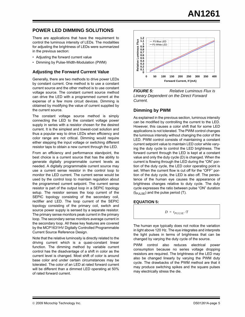
Note that the relative luminosity is directly related to thedriving current which is a quasi-constant linearfunction. The dimming method by variable currentcontrol has the disadvantage of a shift in color as thecurrent level is changed. Most shift of color is aroundbase color and under certain circumstances may betolerated. The color of an LED at rated forward currentwill be different than a dimmed LED operating at 50%of rated forward current.
FIGURE 5: Relative Luminous Flux is Lineary Dependent on the Direct Forward Current.
Dimming by PWMAs explained in the previous section, luminous intensitycan be modified by controlling the current to the LED.However, this causes a color shift that for some LEDapplications is not tolerated. The PWM control changesthe luminous intensity without changing the color of theLED. PWM control consists of maintaining a constantcurrent setpoint value to maintain LED color while vary-ing the duty cycle to control the LED brightness. Theforward current through the LED is kept at a constantvalue and only the duty cycle (D) is changed. When thecurrent is flowing through the LED during the “ON” por-tion of the duty cycle, the LED color operating point isset. When the current flow is cut off for the “OFF” por-tion of the duty cycle, the LED is also off. The persis-tence of the human eye causes the appearance ofbrightness changes relative to duty cycle. The dutycycle expresses the ratio between pulse “ON” duration(tPULSE) and the pulse period (T).
EQUATION 5:
The human eye typically does not notice the variationin light above 120 Hz. The eye integrates and interpretsthe light pulses in terms of brightness that can bechanged by varying the duty cycle of the source.
PWM control also reduces electrical powerconsumption because no series voltage droppingresistors are required. The brightness of the LED mayalso be changed linearly by varying the PWM dutycycle. The drawbacks of the PWM method are that itmay produce switching spikes and the square pulsesmay electrically stress the die.
00.10.20.30.40.50.60.70.80.9
11.11.2
0 50 100 150 200 250 300 350 400Forward Current, If (mA)
Rel
ativ
e Lu
min
ous
Flux P3 Blue LED
P3 White LED
D tPULSE T⁄=
© 2009 Microchip Technology Inc. DS01261A-page 5

AN1261
FIGURE 6: Linearity of Brightness vs. Duty Cycle in PWM LED drive.
MCP1631 PWM CONTROLLERThe MCP1631/MCP1631V is a high-speed pulse widthmodulator (PWM) used to develop intelligent powersystems. When combined with a microcontroller, theMCP1631/MCP1631V will control the powertrain dutycycle to provide output voltage or current regulation. Afunctional block diagram of the PWM controller isshown in Figure 7.
The MCP1631/MCP1631V inputs were developed tobe attached to the I/O pins of a microcontroller. Bycombining the MCP1631/MCP1631V with a low costmicrocontroller, intelligent LED lighting designs can beeasily developed.
The microcontroller is used to adjust the output current,switching frequency and maximum duty cycle. Itprovides additional features that make the powersystem more intelligent, robust and adaptable.
Additional features integrated into the MCP1631HV/MCP1631VHV provide signal conditioning andprotection features for constant current sourceapplications.
The MCP1631 is available in a 20-Lead 4x4 mm QFN,20-Lead TSSOP, or SSOP packages.
Powering the MCP1631For applications that operate from a high voltage input,the MCP1631HV and MCP1631VHV device optionsmay be used. They will operate directly from a +3.5V to+16V input. For these applications, an additional lowdrop out +5V or +3.3V regulated output is available onchip and can provide up to 250 mA of current to powera microcontroller and auxiliary circuits.
High-Speed Analog PWM OperationThe high-speed analog PWM is used to drive theSEPIC powertrain switch to regulate the output of theconverter. Voltage or current may be regulateddepending on what is being sensed. For the SEPICLED driver application, the MCP1631HV is alwaysregulating current. A PIC microcontroller is providingthe oscillator and current references required to obtainthe desired output current.
The PWM signal starts with the PIC generatedoscillator input. When the oscillator input is low, theVEXT driver output pin is pulled high, turning on theexternal N-Channel MOSFET switch.
The current begins to ramp up in the primary coilcurrent sense resistor until the voltage exceeds 1/3 ofthe VREF reference value supplied by themicrocontroller. The VREF voltage is internally limited to0.9V. The 0.9V limit is used as an overcurrent limit. Apassive filter is used on the current sense input (CS) toremove the leading edge turn-on spike associated withthe turn-on of the external power MOSFET. TheMCP1631/MCP1631V internal P-Channel MOSFEToutput driver is powered using a separate PVDD pin tokeep switching noise off of the analog AVDD pin andsensitive current sense circuitry.
The error amplifier (A1 on datasheet diagram) is usedto compare the switch current with the programmedreference current. When the switch current is less thanthe programmed current, the PWM switch driver dutycycle increases. When the switch current is greaterthan the programmed current, the PWM switch driverduty cycle decreases. The PWM duty cycle will trackchanges in output current and adjust the duty cycleaccordingly. The external feedback (FB) andcompensation (COMP) pins are used to control thespeed of the error amplifiers output response.
The MCP1631HV contains a 10V/V inverting gainamplifier (A2) for general purpose use. The A2 currentsense amplifier may be used to amplify the sensecurrent in the secondary side of the SEPIC converter orfreewheeling current in a Buck converter.
Sensing Battery VoltageUsing the microcontroller A/D converter to sense loadvoltage requires a low source impedance to performaccurate readings. Low source impedance requireslow resistance values that would draw excessivecurrent at the converter output, decreasing theefficiency. The MCP1631HV integrates anotheramplifier (A3) configured as a unity gain buffer. Thebuffer provides a high impedance input to the voltagesense divider while also providing a low impedancesource for the microcontroller A/D converter input.
00.10.20.30.40.50.60.70.80.9
1
0 10 20 30 40 50 60 70 80 90 100Duty Cycle, D (%)
Rel
ativ
e Lu
min
ous
Flux
DS01261A-page 6 © 2009 Microchip Technology Inc.

AN1261
Overvoltage ProtectionOvervoltage (OV) protection is a common voltageconvertor protection feature. It is used to protect thepower switch from excessive voltage if the load isremoved. OV protection also prevents accidentalovervoltage at the load if the programmed outputcurrent exceeds the absorption capability of the load.OV protection is typically required for any currentsource application such as battery chargers and LEDdrivers.The MCP1631HV integrates an internal high speed OVcomparator (C2) that uses a 1.2V reference. When thevoltage on the OVIN pin exceeds the 1.2V referencethreshold, the VEXT output is immediately driven low.The VEXT output will be re-enabled once the OVINvoltage has dropped below the 1.2V reference by50 mV. The 50 mV is the typical hysteresis of the OVcomparator.
OSC Disable FeatureThe oscillator disable input (OSCDIS) is used toasynchronously terminate the PWM VEXT output. Thiscan be used along with the shutdown (SHDN) pin anda separate PWM input to modulate current into an LEDfor lighting applications.
© 2009 Microchip Technology Inc. DS01261A-page 7

AN1261
FIGURE 7: MCP1631 PWM Controller - Functional Block Diagram.
MCP1631HV/VHV High Speed PIC PWM
R
S Q
Q
A1+
-VREF
FB
C1+
-
CS/VRAMP
OSCIN
PVDD
COMP
PGND
VEXT
2R
2.7V Clamp
OT
UVLO
100 kΩ
0.1 µA
VDD
R
+
- R
R
10R
+
-
A2
A3
+3.3V or +5.0V LDO 250 mA
VIN
AVDD_OUT / AVDD_IN
VDD
Shutdown ControlA3 Remains OnSHDN
ISIN
ISOUT
VSIN
VSOUT
C2+
-
VDD
AGND
OVIN
Overvoltage Compw/ Hysteresis
Internal1.2V VREF
OSCDIS
100 kΩ
Remove for MCP1631Vand MCP1631VHV Options
Internal Regulator for MCP1631HV and MCP1631VHVOptions Only; For MCP1631 and MCP1631V AVDD_IN is input
VDD
VDD
VDD
VDD
VDD
Note 1: On Shutdown, amplifier A3 remains functional.
2: For HV options, internal Low Drop Out Regulator provides+3.3V or +5.0V bias to VDD.
DS01261A-page 8 © 2009 Microchip Technology Inc.

AN1261
Shutdown FeatureThe MCP1631/MCP1631V shutdown (SHDN) featureis used to disable the device and to minimize thequiescent current draw. While shutdown, amplifier A3remains operational. During shutdown, the devicetypically draws 4.4 µA from the supply source.UnderVoltage Lockout and Thermal ShutdownThe MCP1631/MCP1631V has built-in UnderVoltageLockout (UVLO) that ensures the output VEXT pin isforced to a low state when the input voltage or AVDD isbelow a specified value. This prevents the mainMOSFET switch from being turned on during apower-up or power-down sequence. The MCP1631/MCP1631V provides a thermal shutdown protectionfeature. If the internal junction temperature of thedevice exceeds the overtemperature setpoint limit, theovertemperature protection feature will pull the VEXToutput low to turn off the MOSFET switch.
SEPIC TOPOLOGYWe shall examine the SEPIC topology anddemonstrate the capability of the MCP1631 family incurrent control applications using the SEPIC topology.
The SEPIC Topology (Single Ended Primary InductiveConverter) follows the flyback design, adding acoupling capacitor between the two windings of atransformer.
The output voltage may be lower or higher than theinput voltage, resulting in buck or boost operation.
This topology can use two separate inductors or asingle transformer with two coupled windings. Thecoupled inductor solution saves PCB space andreduces radiated EMI. Another big advantage of usingcoupled inductors is the fact that only half of the calcu-lated inductance needs to be used if the inductors arecoupled. A capacitor connected between the primaryinductor and secondary inductor offers DC isolationand protection against a shorted load. The capacitorclamps the winding leakage inductance energy andeliminates the need for a snubber circuit. The inductorinput smooths the current draw and reduces therequired input filtering.
A single low-side switch reduces MOSFET drivevoltage requirements and current limit protectioncomplexity. The switch current can be sensed using aground referenced sense resistor connected to theMOSFET source pin.
A typical SEPIC converter design that is used with theMCP1631HV PWM controller is shown in Figure 8.
We can visualize the waveforms for a betterunderstanding of how the SEPIC works. We willconsider a coupled inductor SEPIC operating inContinuous Current (CC) mode and refer to Figure 9for this example. L1 and L2 are wound on the samecore. The SEPIC switch (Q1) is turned on at the start ofthe cycle. The current in the primary winding L1 (IL1)will ramp up at a rate of VIN / L1. The current in the sec-ondary winding L2 (IL2) ramps at VCc/L2.
The DC voltage across the isolation capacitor CC (VCc)is equal to VIN. The switch current (Q1) is equal to thesum of IL1 and IL2 during the switch on time. The inputcurrent through L1 is continuous, minimizing the inputripple current compared to other topologies.
FIGURE 8: SEPIC Topology.When Q1 turns off, the stored energy in L1 forces thecurrent to continue flowing through the coupling cap(Cc) and the rectifier (D1) to the output. A secondcurrent flow exists due to L2 releasing it’s storedenergy. Current flows from L2 through the rectifier (D1)to the output. The total rectifier current is the sum of thecurrents flowing through L1 and L2. During theswitch-off time, current flowing through the rectifier tothe output must also replenish the output capacitor(COUT). Looking at the output capacitor currentwaveform (ICc), it can be seen that the output current ofthe SEPIC converter is supplied by the output capacitorwhen the switch is on and supplied by the inductorswhen the switch is off.
The transfer function for the SEPIC converter is derivedin a similar fashion as other switching powertopologies. The volt-time product of the magneticsmust be balanced and the charge-time product on allcapacitors must be balanced for each switch period.
The input block components L1 and Q1 act like astandard boost converter input stage. The output blockcomponents L2, D and COUT act like an invertedbuck-boost converter. The goal is to determine thevolt-time product on the magnetics during the switch ontime and set that equal to the volt-time product on themagnetics during the switch off time.
Basic definitions for design are:
• TSW = Switching Period
© 2009 Microchip Technology Inc. DS01261A-page 9

AN1261
• fSW = Switching Frequency• tON = Switch on time• tOFF = Switch off time• Duty Cycle D = tON / TSW = tON / (tON + tOFF)As D can have values between 0 and 1, the previousequation can be written as: 1 - D = tOFF / (tON + tOFF).
Balance the inductor volt-time product in the booststage (L1).
For Q1 Turned on (+ Slope):
EQUATION 6:
For Q1 Turned off (- Slope):
EQUATION 7:
The inductor current area defined by the slopes mustbe equal for volt-time balance.Solving Equation 6 and Equation 7 by extracting ΔIL1,we will obtain VCc.
EQUATION 8:
As mentioned previously, duty cycle D = tON / (tON +tOFF) or (1 - D) = tOFF / (tON + tOFF). If we multiply bothsides of Equation 8 with 1 / (tON + tOFF), we willintroduce D into the following equation:
EQUATION 9:
EQUATION 10:
The secondary (L2) inductor current area defined bythe slopes must also be equal. The volt-time product issolved similar to the primary inductor volt-time product.
For Q1 Turned on (+ Slope):
EQUATION 11:
FIGURE 9: SEPIC Converter Waveforms.
ΔIL1 tON⁄ VIN L1⁄=
ΔIL1 tOFF⁄VCc VOUT VIN–+
L1--------------------------------------------=
VIN tON× VCc VOUT VIN–+( ) tOFF×=
VIN D× VCc VOUT VIN–+( ) 1 D–( )×=
VCc VIN1
1 D–-------------⎝ ⎠⎛ ⎞× VOUT–=
ΔIL2tON-----------
VCcL2
---------=
DS01261A-page 10 © 2009 Microchip Technology Inc.

AN1261
For Q1 Turned off (- Slope):EQUATION 12:
As above, we’ll solve Equation 11 and Equation 12 forVCc.
Inductor slope's must be equal for volt-time balance,so:
EQUATION 13:
As shown above, duty cycle D can be introduced inEquation 13 by multiplying both sides with 1 / (tON +tOFF):
EQUATION 14:
Setting Equation 10 equal to Equation 14 yields:
EQUATION 15:
The solution for VOUT/VIN is the transfer function of theSEPIC converter in continuous mode:
EQUATION 16:
By rearranging Equation 16 we get VIN = VOUT x (1-D)/D. Substituting that result into Equation 14 results in:
EQUATION 17:
The voltage across the coupling capacitor (Cc) is equalto VIN. This occurs as long as the capacitance of COUTis adequate to supply the output current during theswitch ON time and the system operates in continuouscurrent mode.
Until now, the diode forward voltage drop (VD) hasbeen ignored at the output because of its low value. Ifthe output voltage is low, the forward voltage drop ofthe diode may be significant. When the diode drop isconsidered, the maximum duty cycle will be:
EQUATION 18:
The first step in calculating the inductor current is toknow the maximum output power required. Anefficiency estimate of 85% for a SEPIC converter canbe used to approximate the input current. The averageinput current is equal to the input power divided by theinput voltage.
EQUATION 19:
EQUATION 20:
EQUATION 21:
The inductor value is calculated by:
EQUATION 22:
ΔIL is the desired inductor peak to peak ripple current.A good ΔIL approximation is 20% of the output current.The approximate ripple current for a 1A output currentwould be 200 mA.
If L1 and L2 are wound on the same core, which is thecase of this SEPIC design, the value of inductance inthe equation above is replaced by (1/2)L due to mutualinductance.
EQUATION 23:
The maximum inductor current (ripple and peaks for L1and L2) can be calculated to avoid saturating theinductor.
EQUATION 24:
ΔIL2tOFF-----------
VOUTL2
-------------=
tON VCc× tOFF VOUT×=
VCc VOUT1 D–
D-------------⎝ ⎠⎛ ⎞×=
VCc VIN1
1 D–-------------⎝ ⎠⎛ ⎞ VOUT–× VOUT
1 D–D
-------------⎝ ⎠⎛ ⎞×= =
VOUTVIN
------------- D1 D–-------------⎝ ⎠⎛ ⎞=
VCc VIN=
Dmax VOUT VD+( ) VINmin VOUT VD+ +( )⁄=
POUT VOUT IOUT×=
PIN POUT Efficiency( )⁄=
IIN AVG( ) PIN VIN⁄=
L1 L2 VINmin Dmax×( ) ILΔ fSW×( )⁄= =
L2--- VINmin Dmax×( ) 2 ILΔ fSW×( )( )⁄=
IL1ONΔ VIN tON×( ) L 2⁄( )⁄=
© 2009 Microchip Technology Inc. DS01261A-page 11

AN1261
EQUATION 25:EQUATION 26:
EQUATION 27:
The coupled inductor winding currents calculatedabove are used to determine the wire size and core ofthe inductor. High switching frequency has severaladvantages: smaller ripple current, lower peak andRMS current and lower volt-time product on theinductor core. This leads to smaller and lower-costsolutions.
The switch current (IQ1) is equal to the combination ofthe winding currents during the switch on time. Whenthe switch is turned on, it conducts the current from L1and L2.
EQUATION 28:
The peak Q1 switch voltage is equal to VIN + VOUT forthe SEPIC converter. Any leakage inductance voltagespike is clamped through the output diode by the outputcapacitor. A switch voltage rating for applicationsshould be at least:
EQUATION 29:
The maximum reverse voltage across the SEPIC diodeoccurs during the switch ON time. The cathode of theschottky diode is connected to VOUT, the anode of theschottky diode is connected to the SEPIC couplingcapacitor. The voltage across the coupling capacitorvoltage is equal to VIN. When Q1 is ON, the voltageacross the diode is:
EQUATION 30:
A schottky diode is recommended for low voltageapplications because of the low forward voltage drop.The lower forward drop improves converter efficiency.
The selection of the SEPIC capacitor, Cc, depends onthe RMS current, which is passing through it. The RMScurrent in the SEPIC coupling capacitor is mainlydependant upon output power with some influence byinductor ripple current. The RMS current in Cc can becalculated by solving Equation 31 for both states ofswitching, tON and tOFF. Equation 32 is the RMSexpression of a trapezoid waveform.
EQUATION 31:
EQUATION 32:
where I1 is the lowest waveform current and I2 is thehighest waveform current: I1=IAVG + (Iripple / 2) andI2=IAVG - (Iripple / 2). For Q1 turned on IAVG = IOUT andIripple = tON x 2VIN / (4L). For Q1 turned off IAVG = -IINand Iripple = tOFF x 2VIN / (4L).
To estimate the size for the coupling capacitor, thecapacitor derivative equation can be used.
EQUATION 33:
For the SEPIC converter, the coupling capacitorvoltage is approximated as a DC value when derivingthe duty cycle. The ripple voltage should be no morethan a few percent (5% in practice) of the voltageacross the capacitor or the input voltage. The SEPICcapacitor must be rated for a large RMS current inrelation to the output power. As the output powerincreases, the capacitor ripple current will increase aswell. This makes the SEPIC converter better suited forlower power applications where the RMS currentthrough the capacitor is relatively small. The worst caseRMS current in the coupling capacitor will occur atmaximum output power and minimum input voltage.
EQUATION 34:
The same algorithm should to be applied to the outputcapacitor. Ripple voltage (ΔV or Vripple) should be nomore than a few percent of the voltage across thecapacitor. When the switch is on (tON = D / fSW), theinductor L1 is charging and the output current issupplied by the output capacitor COUT.
IL1peak IIN AVG( ) IL1ON 2⁄Δ+=
IL2ONΔ VIN tON×( ) L 2⁄( )⁄=
IL2peak IOUT AVG( ) IL2ON 2⁄Δ+=
Iswitch Q1( ) IL1 IL2+=
Vswitch Q1( ) VINmax VOUTmax+=
VD VOUT VIN VOUT VCc+( )=+=
ICcRMS ICcRMS ON–2 ICcRMS OFF–
2+=
ICcRMS ON OFF( )– D I( 12× I1 I2×( ) I2
2+ + ) 3⁄=
C ICtΔVΔ
-------×=
CcIOUTVCcΔ
-------------⎝ ⎠⎛ ⎞ Dmax
fSW-------------⎝ ⎠⎛ ⎞×=
DS01261A-page 12 © 2009 Microchip Technology Inc.

AN1261
EQUATION 35:The input capacitor CIN should be capable of handlingthe input RMS current. The input current waveform iscontinuous and triangular. The inductive input ensuresthat the input capacitor sees low ripple currents fromthe power supply. The input capacitor provides a lowimpedance source for the SEPIC converter in caseswhere the power source is not immediately adjacent tothe SEPIC powertrain.
MCP1631HV PROGRAMMED CURRENT SOURCE REFERENCE DESIGN FOR DIMMING POWER LEDSMicrochip has developed a reference design for adimmable power LED lighting application todemonstrate the capability of the MCP1631HV PWMController.
The MCP1631HV Digitally Controlled ProgrammableCurrent Source board (MCP1631RD-DCPC1) is usedto drive and dim one or more power LEDs in series orparallel topology. The board uses the PIC16F616microcontroller to generate the proper dimming ratio.The default dimming ratio is set at 10:1. The dimmingratio and maximum current are selected beforecompiling the source code. The firmware on thedevelopment board is programmed for 700 mA of LEDdrive current. An LED load capable of handling 700 mAof current is required to use the supplied firmware.Lower drive currents may be obtained by downloadingthe firmware source code from Microchip’s website andchanging the drive current parameter in the header file.The source code is then compiled and downloaded tothe development board. The minimum programmedcurrent that the board can generate is 70 mA. An LEDfrom XLamp® XR-E series (Cree®) can be used toevaluate the board. The LED can be supplied with700 mA or 1000 mA, based on the selected model. Asexample, the XRWWHT-L1-0000-009E7 warm whiteLED can be driven at 700 mA maximum.
LED indicators on the reference design provide statusand fault indication (i.e.: overvoltage, overtemperature,thermal shutdown).
TABLE 1: DEFAULT OUTPUT CAPABILITY OF MCP1631HV LED DRIVER REFERENCE BOARD
The reference board is capable of driving 1A maximum@ 8.5W output power. Efficiency is typical 85% atmaximum power. The default parameters are displayedin Table 1.
An input terminal block is provided for connecting theinput source voltage to the board. An output header isalso provided for attaching the load LED and anexternal 10k thermistor. The thermistor should bemounted on the LED heat sink near the LED. Thetemperature monitoring feature must be enabled in thesource code before compiling. The default value forovertemperature shutdown is 40oC. Temperaturemonitoring is not enabled in the default .hex file. Therecommended thermistor is EPCOS Inc. PNB57703M0103G040.
A Microchip ICD2 / PICkit 2 compatible programmingheader is available for updating the reference boardfirmware contained within the PIC16F616. ThePIC16F616 microcontroller is used to regulate outputvoltage, current, switching frequency and maximumduty cycle. The MCP1631HV generates the requiredswitch duty cycle and provides fast overcurrentprotection based upon the various external inputs.External signals include the reference oscillator, the
reference voltage, the feedback voltage and the currentsense. The output drive signal is a square-wave pulseused to drive the gate of the powertrain MOSFETswitch. The power train topology used for theMCP1631HV Programmable Current Source is aSingle-Ended Primary Inductive Converter (SEPIC).
The MCP1631HV Programmable Current Source hasthe following features:
• Input Operating Voltage Range: +3.5V to +16V• Maximum output current 700 mA with dimming
ratio 10:1 (70 mA/step for pre-compiled.hex file)• Drive one or more power LEDs. Limited by OVP
and 8.5W power capability• Optional battery charger software on Microchip
website for charging Li-Ion, NiMH, and NiCd battery packs. Charge 1 or 2 single cell Li-Ion batteries in series or 1 to 4 single cell NiMH or NiCd batteries in series
• Maximum output capability for all modes of operation: 1A @ 8.5W
• ON/OFF/Dimming switch• Status Indication• Hardware and software overvoltage shutdown set
at 9.0V
COUTIOUT
Vripple----------------⎝ ⎠⎛ ⎞ D
fSW--------⎝ ⎠⎛ ⎞×=
Programmed output current (Note 1) Dimming ratio Max. Output power
(Note 1)Over voltage
protectionThermal
shutdown (Note 2)
700 mA 10:1 8.5W 9V 40°CNote 1: Maximum programmed output current in the source code is 1A. Total power output should not exceed
8.5W.
2: This option is not enabled in default compiled .hex file available on the Microchip website.
© 2009 Microchip Technology Inc. DS01261A-page 13

AN1261
FIGURE 10: Output Current Regulation vs. Input Voltage in Driving LED Mode.
OperationThe MCP1631HV Digitally Controlled ProgrammableCurrent Source Reference Design has a red/green dualcolor LED (D2) to indicate status and faults. The greenLED will flash with a one second period when thesystem is activated and current is being supplied to theload.Press button S1 to enable the output and drive the LEDwith the minimum programmed current of 70 mA. Eachadditional press of S1 will increment the drive currentby 10% of the final programmed value. Press and holdS1 for at least 2 seconds until the red LED indicator isactivated to switch the output current off. If a faultcondition such as no load, overvoltage, orovertemperature is present when attempting to turn theoutput on, the system will stay off and the faultcondition will be indicated by the flashing red indicatorLED. The faults are coded as following:• Red LED flashes at 1 Hz rate if an overtempera-
ture of the LED case has been detected. The fault is Thermal Shutdown
• Red LED flashes at 2 Hz rate if an overvoltage or a missing/open load has been detected. The fault is Overvoltage Shutdown
An overvoltage/overtemperature fault condition will beverified 5 times by the microcontroller firmware beforethe fault is validated and the system shuts down.Two parallel resistors, R10 and R11, are used to sensethe MOSFET switch (Q1) current (Figure 11). Thecurrent sense signal is applied to the CS comparatorinput of MCP1631HV. The load current is equal to thecurrent in the secondary inductor L1:B. Sense resistorsR2 and R3 are used to sense the load current. The loadsense signal is amplified by the ISin current senseamplifier before entering the feedback pin (FB). Areference voltage signal from the PIC16F616 suppliesthe VREF current reference voltage for theMCP1631HV. The pulse width modulated VEXT signalthat drives the MOSFET switch is generated by theMCP1631HV using the microcontroller currentreference PWM signal and the load current feedbacksignal. The current feedback signal is integrated withthe current reference signal. The integrated signal is
compared with the switch current sense and an artificialcompensation ramp to modulate the switch drivesignal. The artificial compensation ramp is generatedfrom the PIC16F616 OSC output signal to prevent thesystem from switching between continuous anddiscontinuous operation. The bi-modal operation wouldcause the duty cycle to vary when D > 50%. Theartificial ramp voltage supplements the switch currentsense voltage to guarantee the CS signal rises abovethe reference signal before the end of the integratorperiod. When the CS signal rises above the referencesignal, the MOSFET switch will be turned off, resetingthe integrator. The artificial ramp slope for the SEPICwill be the same as the slope of the current during theOFF time of the oscillator. The artificial ramp circuitblock consists of C10, R9, R13, and Q2 which is drivenwith the OSC signal.
A resistor divider network composed of R5, R8, and R15is used for load voltage sensing. R5 sensesovervoltage conditions and feeds directly into theMCP1631HV overvoltage input pin. R8 senses the loadvoltage. The load voltage tap at R8 is connected to theMCP1631HV internal voltage follower amplifier via theVSIN pin. The corresponding VSout signal is fed to thePIC16F616 A/D RA2 port.
When a thermistor is used, it is placed across J2-4 andJ2-5. The thermistor forms a voltage divider with R1, a10 kΩ resistor. The voltage across the thermistor is fedto the A/D port RA4 of the PIC16F616. If anovertemperature condition is detected, themicrocontroller will disable the PWM signal ofMCP1631.
The OSC signal is generated directly by thePIC16F616 PWM hardware at port RC5.
MCP1631HV Digitally Controlled Programmable Current Source Reference Design FirmwareThe source code for Microchip’s MCP1631HV DigitallyControlled Programmable Current Source ReferenceDesign was developed using mikroElektronica’s Mik-roC Compiler for PIC Processors. The software hasconditional compiler options for user selectableparameters and function. The LED driver is the defaultcompiler option. The NiMH/NiCd and Li-Ion batterycharger options are selectable at compile time bymodifying a parameter in the header file. The mikroCcompiler may be downloaded at: http://www.mikroe.com.
Please consult the mikroC website and compiler Helpfor more information about the compiler.
00.10.20.30.40.50.60.7
0 1 2 3 4 5 6 7 8 9 10 11 12 13 14 15 16Input Voltage (V)
Out
put C
urre
nt (A
)
3W White LED @ 700mA3W Amber LED @ 700mA3W Amber LED @ 350mA2 series 3W White LEDs @ 700mA
DS01261A-page 14 © 2009 Microchip Technology Inc.

AN1261
FIGURE 11: MCP1631HV Programmable LED Current Source Reference Design Schematic.
M
3
1
2
5
8 3
4
67
12
© 2009 Microchip Technology Inc. DS01261A-page 15

AN1261
FIGURE 12: Top Silk and Pads of Reference Design.
FIGURE 13: Top Layer of Reference Design.
FIGURE 14: Bottom Layer of Reference Design.The reference board PIC16F616 microcontroller hasbeen pre-programmed with the LED driver option. Thereference board may also be operated as a batterycharger. The user may re-configure and compile thesource code for Li-Ion or NiMH/NiCd battery charginginstead of LED driving.
The firmware packet has several files for LED dimmingand battery charging.
• LED = 00234R1.hex• Li-Ion = 00234R1-LiIon_Charger.hex• NiMH = 00234R1-NiMH_NiCd_Charger.hex• NiCd = 00234R1-NiMH_NiCd_Charger.hex
The C source code file is 00234R1.c and the headerfile is 00234R1.h. These two files are referenced bythe mikroC project file: 00234R1.ppc.
To setup the parameters, the user starts with the00234R1.h file. Set the function of interest for thereference board as enabled. The example below is foran LED driver./* Enable support for Lithium Ion batteries */ #define LION_SUPPORT DISABLED
/* Enable support for Nickel Metal Hydride batteries */ #define NIMH_SUPPORT DISABLED
/* Enable support for LED Driver */
#define LED_DRIVER_SUPPORT ENABLED
The charging/driving current profile parameters are setin separate sections of the header file for the project.The LED driver overvoltage value is set to 9V byparameter LED_DRIVER_OVER_VOLTAGE. The LEDdriver starting current value is set to 70 mA byparameter LED_DRIVER_CONDITION_CURRENT.The LED maximum current value is set to 700 mA byparameter LED_DRIVER_CURRENT. To evaluate theboard, a Cree XREWHT-L1-0000-009E7 with warmwhite LEDs that can be driven at 700 mA maximumshould be used. The overtemperature setpoint isenabled by setting OVERTEMPERATURE_SUPPORT toENABLED. The default overtemperature set point is+40°C.
A 10k NTC thermistor must be connected betweenJ2-4 and J2-5 of the J2 connector whenovertemperature support is enabled. The thermistorshould be placed as close as possible to the LEDmounting area. The number of LEDs value is set to 1by parameter NUMBER_OF_CELLS_DEFAULT. Thesedefault values are for a typical 3W power LED.#if (LED_DRIVER_SUPPORT == ENABLED) // define the LED Driver characteristics in millivolts and // milliamps). Default values are for one 3W/750mA Power LED // with max forward voltage 4.5V
/* LED overvoltage */ #define LED_DRIVER_OVER_VOLTAGE ((int)(9000.0/BATTERY_MV_PER_BIT))
/* cell conditioning/startup current = 70 mA */ #define LED_DRIVER_CONDITION_CURRENT ((int)(70.0/BATTERY_MA_PER_BIT))
/* total charge current = 700 milliamps */ #define LED_DRIVER_CURRENT ((int)(700.0/BATTERY_MA_PER_BIT))
/* LED overtemperature limit = 40 deg C (40 / 0.1447) = 311 */ #define LED_DRIVER_OVTEMP_SETPOINT ((float)(THERMISTOR_OHMS_40C))
/* ENABLE or DISABLE the overtemperture detection */
#define OVERTEMPERATURE_SUPPORT DISABLED
/* default number of LEDs in series topology */
#define NUMBER_OF_CELLS_DEFAULT 1
#endif /* LED_DRIVER_SUPPORT */
DS01261A-page 16 © 2009 Microchip Technology Inc.

AN1261
The OSC reference signal supplied to the MCP1631HVPWM controller is set by the PIC16F616. Thefrequency may be set to 200 kHz or 500 kHz. Theparameters are set in the main C file 00234R1.c./* define Oscillator Output PWM frequency Prescale Valuefor PR2 */#define OSC_500KHZ_PR2_REG 0x03
#define OSC_200KHZ_PR2_REG 0x09
#define OSC_PR2_REG OSC_500KHZ_PR2_REG
The oscillator duty cycle is set to 25% if the SEPICreference board must work in buck-boost mode. The25% duty cycle allows the system to boost the outputvoltage. The parameter is in the 00234R1.h headerfile. /* charge oscillator duty cycle */
#define OSCILLATOR_DUTY_CYCLE 25
The number of incremental LED current steps is set to10 by the parameter IREF_INCREMENTS. Each S1button press will increment the output current by afactor of (1 / IREF_INCREMENTS) times theprogrammed current value up to the programmedcurrent value./* define Reference Current Increments when rampingup current at startup */
/* rate is 1 increment every second in Charger Modeor every button push for LED Driver */
#define IREF_INCREMENTS 10
Example:
The MCP1631RD-DCPC1 Reference Board needs todrive an LED string composed of 2 white LEDs in seriestopology with a 350 mA maximum forward current. Theboard is powered from a 12V source.
Solution:
The system will need to provide 1 LED x 350 mA =350 mA of drive current, because the LEDs areconnected in series topology.
IREF_INCREMENTS is set to 10 to allow 10incremental current steps.
LED_DRIVER_CONDITION_CURRENT is set to thestartup current value of 35 mA.
LED_DRIVER_CURRENT is set to the final current of350 mA.
LED_DRIVER_OVER_VOLTAGE is set to 8V which isthe sum of maximum forward voltages of the two whiteLEDs.
The system will only need to operate in buck modebecause the 12V power supply voltage is greater thanthe 8V load voltage.
OSCILATOR_DUTY_CYCLE is set to 50% for buckmode.
OVERTEMPERATURE_SUPORT is set to DISABLEDbecause cooling the LED string is not an issue.
The flowchart of the default source code is given inFigure 15. When powered on, the microcontrollerinitializes the ports and the default system parameters.If push-button S1 is pressed, the load is supplied withcondition current. Each additional press of S1 willincrease the current until the maximum programmedcurrent is reached. Further presses will not increasethe current beyond the maximum value. When S1 ispressed and held for more than 2 seconds, the red LEDwill turn on and the output will turn off.
© 2009 Microchip Technology Inc. DS01261A-page 17

AN1261
FIGURE 15: Firmware Flow Diagram for LED Driver With Dimming.
START
Initialize: Processor, Parameters
No
Yes
END
OVP Test VOUT> 9.0V?
No
Fault
OVPtime retries
> 5
Yes
(ILEDmin = 70 mA, ILEDmax = 700 mA),
Timers, Sample ADC()
Shutdown
Shutdown
S1 Pressed?
Yes
No
Increment IREF(70 mA)
S1 pressed 2s?>=
Yes
No
S1 Pressed?
No
Yes
ILEDmin
DS01261A-page 18 © 2009 Microchip Technology Inc.

AN1261
CONCLUSIONFor applications that require intelligent powermanagement solutions like LED drivers, thecombination of a microcontroller and the MCP1631high-speed PWM is very powerful. It brings theprogrammability benefits of the microcontroller andadds the performance of a high speed analog PWM.The analog PWM will respond to changes in inputvoltage and output current very quickly. Themicrocontroller is used for programmability, forestablishing LED current, for monitoring the circuit forfault conditions, and for taking the appropriate action inthe event of a specific fault.
REFERENCES1. Terry Cleveland, “Using the MCP1631 Family todevelop Low-Cost Battery Chargers”, AN1137,Microchip Technology Inc.
2. Terry Cleveland, “New components and designmethods bring intelligence to battery chargers”,AN960, Microchip Technology Inc.
3. ***, “MCP1631/HV/MCP1631V/VHV Data Sheet”,DS22063, Microchip Technology Inc.
4. Markus Hofmann, “Comparation of LED Circuits”,Application Notes, OSRAM Opto Semiconductor.
5. ***, “Controlling Luminous Intensity of LEDs”,Application Notes, STS-KSE3692, NIKIA.
6. Hubert Ott, Ludwig Plotz, “Dimming InGaN LEDs”,Application Notes, OSRAM Opto Semiconductor.
7. J. Reill, M. Wicke, “Dimming LEDs with respect ofgrouping current”, Application Notes, OSRAM OptoSemiconductor.
8. ***, “Thermal design consideration for Luxeon 5WPower Light sources”, AB23, Lumileds Lighting.
9. ***, “Thermal Management guide”, Rev. 3,Application Notes, Seoul Semiconductor.
10. Rainer Huber, “Thermal Management of SMTLED”, Application Notes, OSRAM OptoSemiconductor.
11. ***, “Electrical Drive Management”, Rev. 1,Application Notes, Seoul Semiconductor.
12. ***, The National Technology Laboratory, website:www.netl.doe.gov.
© 2009 Microchip Technology Inc. DS01261A-page 19

AN1261
NOTES:DS01261A-page 20 © 2009 Microchip Technology Inc.

Note the following details of the code protection feature on Microchip devices:• Microchip products meet the specification contained in their particular Microchip Data Sheet.
• Microchip believes that its family of products is one of the most secure families of its kind on the market today, when used in the intended manner and under normal conditions.
• There are dishonest and possibly illegal methods used to breach the code protection feature. All of these methods, to our knowledge, require using the Microchip products in a manner outside the operating specifications contained in Microchip’s Data Sheets. Most likely, the person doing so is engaged in theft of intellectual property.
• Microchip is willing to work with the customer who is concerned about the integrity of their code.
• Neither Microchip nor any other semiconductor manufacturer can guarantee the security of their code. Code protection does not mean that we are guaranteeing the product as “unbreakable.”
Code protection is constantly evolving. We at Microchip are committed to continuously improving the code protection features of ourproducts. Attempts to break Microchip’s code protection feature may be a violation of the Digital Millennium Copyright Act. If such actsallow unauthorized access to your software or other copyrighted work, you may have a right to sue for relief under that Act.
DS01261AInformation contained in this publication regardingdevice applications and the like is provided only for your conve-nience and may be superseded by updates. It is your responsi-bility to ensure that your application meets with yourspecifications. MICROCHIP MAKES NO REPRESENTA-TIONS OR WARRANTIES OF ANY KIND WHETHEREXPRESS OR IMPLIED, WRITTEN OR ORAL, STATUTORYOR OTHERWISE, RELATED TO THE INFORMATION,INCLUDING BUT NOT LIMITED TO ITS CONDITION,QUALITY, PERFORMANCE, MERCHANTABILITY ORFITNESS FOR PURPOSE. Microchip disclaims all liabilityarising from this information and its use. Use of Microchipdevices in life support and/or safety applications is entirely atthe buyer’s risk, and the buyer agrees to defend, indemnify andhold harmless Microchip from any and all damages, claims,suits, or expenses resulting from such use. No licenses areconveyed, implicitly or otherwise, under any Microchipintellectual property rights.
© 2009 Microchip Technology Inc.
Trademarks
The Microchip name and logo, the Microchip logo, dsPIC, KEELOQ, KEELOQ logo, MPLAB, PIC, PICmicro, PICSTART, rfPIC and UNI/O are registered trademarks of Microchip Technology Incorporated in the U.S.A. and other countries.
FilterLab, Hampshire, HI-TECH C, Linear Active Thermistor, MXDEV, MXLAB, SEEVAL and The Embedded Control Solutions Company are registered trademarks of Microchip Technology Incorporated in the U.S.A.
Analog-for-the-Digital Age, Application Maestro, CodeGuard, dsPICDEM, dsPICDEM.net, dsPICworks, dsSPEAK, ECAN, ECONOMONITOR, FanSense, HI-TIDE, In-Circuit Serial Programming, ICSP, ICEPIC, Mindi, MiWi, MPASM, MPLAB Certified logo, MPLIB, MPLINK, mTouch, Omniscient Code Generation, PICC, PICC-18, PICkit, PICDEM, PICDEM.net, PICtail, PIC32 logo, REAL ICE, rfLAB, Select Mode, Total Endurance, TSHARC, WiperLock and ZENA are trademarks of Microchip Technology Incorporated in the U.S.A. and other countries.
SQTP is a service mark of Microchip Technology Incorporated in the U.S.A.
All other trademarks mentioned herein are property of their respective companies.
© 2009, Microchip Technology Incorporated, Printed in the U.S.A., All Rights Reserved.
Printed on recycled paper.
DS01261A-page 21
Microchip received ISO/TS-16949:2002 certification for its worldwide headquarters, design and wafer fabrication facilities in Chandler and Tempe, Arizona; Gresham, Oregon and design centers in California and India. The Company’s quality system processes and procedures are for its PIC® MCUs and dsPIC® DSCs, KEELOQ® code hopping devices, Serial EEPROMs, microperipherals, nonvolatile memory and analog products. In addition, Microchip’s quality system for the design and manufacture of development systems is ISO 9001:2000 certified.

DS01261A-page 22 © 2009 Microchip Technology Inc.
AMERICASCorporate Office2355 West Chandler Blvd.Chandler, AZ 85224-6199Tel: 480-792-7200 Fax: 480-792-7277Technical Support: http://support.microchip.comWeb Address: www.microchip.comAtlantaDuluth, GA Tel: 678-957-9614 Fax: 678-957-1455BostonWestborough, MA Tel: 774-760-0087 Fax: 774-760-0088ChicagoItasca, IL Tel: 630-285-0071 Fax: 630-285-0075ClevelandIndependence, OH Tel: 216-447-0464 Fax: 216-447-0643DallasAddison, TX Tel: 972-818-7423 Fax: 972-818-2924DetroitFarmington Hills, MI Tel: 248-538-2250Fax: 248-538-2260KokomoKokomo, IN Tel: 765-864-8360Fax: 765-864-8387Los AngelesMission Viejo, CA Tel: 949-462-9523 Fax: 949-462-9608Santa ClaraSanta Clara, CA Tel: 408-961-6444Fax: 408-961-6445TorontoMississauga, Ontario, CanadaTel: 905-673-0699 Fax: 905-673-6509
ASIA/PACIFICAsia Pacific OfficeSuites 3707-14, 37th FloorTower 6, The GatewayHarbour City, KowloonHong KongTel: 852-2401-1200Fax: 852-2401-3431Australia - SydneyTel: 61-2-9868-6733Fax: 61-2-9868-6755China - BeijingTel: 86-10-8528-2100 Fax: 86-10-8528-2104China - ChengduTel: 86-28-8665-5511Fax: 86-28-8665-7889China - Hong Kong SARTel: 852-2401-1200 Fax: 852-2401-3431China - NanjingTel: 86-25-8473-2460Fax: 86-25-8473-2470China - QingdaoTel: 86-532-8502-7355Fax: 86-532-8502-7205China - ShanghaiTel: 86-21-5407-5533 Fax: 86-21-5407-5066China - ShenyangTel: 86-24-2334-2829Fax: 86-24-2334-2393China - ShenzhenTel: 86-755-8203-2660 Fax: 86-755-8203-1760China - WuhanTel: 86-27-5980-5300Fax: 86-27-5980-5118China - XiamenTel: 86-592-2388138 Fax: 86-592-2388130China - XianTel: 86-29-8833-7252Fax: 86-29-8833-7256China - ZhuhaiTel: 86-756-3210040 Fax: 86-756-3210049
ASIA/PACIFICIndia - BangaloreTel: 91-80-3090-4444 Fax: 91-80-3090-4080India - New DelhiTel: 91-11-4160-8631Fax: 91-11-4160-8632India - PuneTel: 91-20-2566-1512Fax: 91-20-2566-1513Japan - YokohamaTel: 81-45-471- 6166 Fax: 81-45-471-6122Korea - DaeguTel: 82-53-744-4301Fax: 82-53-744-4302Korea - SeoulTel: 82-2-554-7200Fax: 82-2-558-5932 or 82-2-558-5934Malaysia - Kuala LumpurTel: 60-3-6201-9857Fax: 60-3-6201-9859Malaysia - PenangTel: 60-4-227-8870Fax: 60-4-227-4068Philippines - ManilaTel: 63-2-634-9065Fax: 63-2-634-9069SingaporeTel: 65-6334-8870Fax: 65-6334-8850Taiwan - Hsin ChuTel: 886-3-6578-300Fax: 886-3-6578-370Taiwan - KaohsiungTel: 886-7-536-4818Fax: 886-7-536-4803Taiwan - TaipeiTel: 886-2-2500-6610 Fax: 886-2-2508-0102Thailand - BangkokTel: 66-2-694-1351Fax: 66-2-694-1350
EUROPEAustria - WelsTel: 43-7242-2244-39Fax: 43-7242-2244-393Denmark - CopenhagenTel: 45-4450-2828 Fax: 45-4485-2829France - ParisTel: 33-1-69-53-63-20 Fax: 33-1-69-30-90-79Germany - MunichTel: 49-89-627-144-0 Fax: 49-89-627-144-44Italy - Milan Tel: 39-0331-742611 Fax: 39-0331-466781Netherlands - DrunenTel: 31-416-690399 Fax: 31-416-690340Spain - MadridTel: 34-91-708-08-90Fax: 34-91-708-08-91UK - WokinghamTel: 44-118-921-5869Fax: 44-118-921-5820
WORLDWIDE SALES AND SERVICE
03/26/09