Digitally Programmable Delay-Locked-Loop with Adaptive ... · Digitally Programmable...
66
UNIVERSIDADE NOVA DE LISBOA Faculdade de Ciências e Tecnologia Departamento de Engenharia Electrotécnica e de Computadores Digitally Programmable Delay-Locked-Loop with Adaptive Charge Pump Current for UWB Radar System por Bruno Miguel Lopes Dissertação apresentada na Faculdade de Ciências e Tecnologia da Universidade Nova de Lisboa para obtenção do grau de Mestre em Engenharia Electrotécnica e Computadores. Orientador: Nuno Filipe V. Paulino 2010
Transcript of Digitally Programmable Delay-Locked-Loop with Adaptive ... · Digitally Programmable...

UNIVERSIDADE NOVA DE LISBOA
Faculdade de Ciências e TecnologiaDepartamento de Engenharia Electrotécnica e de Computadores
Digitally Programmable Delay-Locked-Loopwith Adaptive Charge Pump Current for
UWB Radar System
por
Bruno Miguel Lopes
Dissertação apresentada na Faculdade de Ciências e Tecnologia daUniversidade Nova de Lisboa para obtenção do grau deMestre em Engenharia Electrotécnica e Computadores.
Orientador: Nuno Filipe V. Paulino
2010

Acknowledgements
It was a long road until the end of this thesis, nevertheless I would never have had finishedit without the support, patience and love from my family. A special kiss and hug to mydear sister because she will always be a part of my life.
When I ear the word teacher, the first name that occurs to me is of my advisor, ProfessorNuno Paulino whose support and knowledge made this thesis possible. It was a greatpleasure having him as my advisor.
For last, but with a great importance in my life, to Cintia the love of my life. Thanks foreverything.
1


UNIVERSIDADE NOVA DE LISBOA
AbstractFaculdade de Ciências e Tecnologia
Departamento de Engenharia Electrotécnica e de Computadores
Mestre em Engenharia Electrotécnica e de Computadores
by Bruno Miguel Lopes
The objective of this thesis is to study and design a digitally programmable delay lockedloop for a UWB radar sensor in 0.13 µm CMOS technology.. Almost all logic systemshave a main clock signal in order to provide a common timing reference for all of thecomponents in the system. In certain cases it is necessary to have rising (or falling) edgesat precise time instants, different from the ones in the main clock. To create those newtiming edges at the appropriate time it is necessary to use delay circuits or delay lines.In the case of the radar system its necessary to generate a clock signal with a variabledelay. This delay is relative to the transmit clock signal and is used to determine thetarget distance. Traditionally, delay lines are realized using a cascade of delay elementsand are typically inserted into a delay-locked-loop (DLL) to guaranty that the delay isnot affected by process and temperature variations. A DLL works in a similar way to aPhase Locked Loop (PLL).In order to facilitate the operation of the radar system, it is important that the delayvalue should be digitally programmable. To achieve a digitally programmable delay witha large linearity (independent from matching errors), the architecture of the system isconstituted by a digital Σ∆ modulator that controls a 1-bit digital to time converter,whose output will be filtered by the DLL, thus producing the delayed clock signal.The electronic sub-blocks necessary to build this circuit are describe in detail as theproposed architectures. These circuits are implemented using differential clock signals inorder to reduce the noise level in the radar system. Design and simulation results of thedigitally programmable DLL shows a high output jitter noise for large delays. In order toimprove this results a new architecture is proposed. Conventional DLL’s have a predefinedcharge pump current. The new architecture will make the charge pump current variable.Simulations results will show a improved jitter noise and delay error.
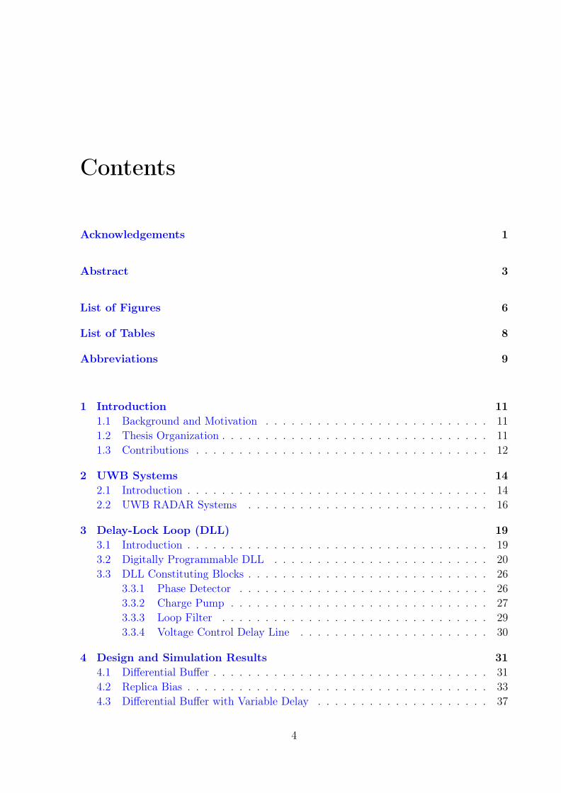
Contents
Acknowledgements 1
Abstract 3
List of Figures 6
List of Tables 8
Abbreviations 9
1 Introduction 111.1 Background and Motivation . . . . . . . . . . . . . . . . . . . . . . . . . . 111.2 Thesis Organization . . . . . . . . . . . . . . . . . . . . . . . . . . . . . . . 111.3 Contributions . . . . . . . . . . . . . . . . . . . . . . . . . . . . . . . . . . 12
2 UWB Systems 142.1 Introduction . . . . . . . . . . . . . . . . . . . . . . . . . . . . . . . . . . . 142.2 UWB RADAR Systems . . . . . . . . . . . . . . . . . . . . . . . . . . . . 16
3 Delay-Lock Loop (DLL) 193.1 Introduction . . . . . . . . . . . . . . . . . . . . . . . . . . . . . . . . . . . 193.2 Digitally Programmable DLL . . . . . . . . . . . . . . . . . . . . . . . . . 203.3 DLL Constituting Blocks . . . . . . . . . . . . . . . . . . . . . . . . . . . . 26
3.3.1 Phase Detector . . . . . . . . . . . . . . . . . . . . . . . . . . . . . 263.3.2 Charge Pump . . . . . . . . . . . . . . . . . . . . . . . . . . . . . . 273.3.3 Loop Filter . . . . . . . . . . . . . . . . . . . . . . . . . . . . . . . 293.3.4 Voltage Control Delay Line . . . . . . . . . . . . . . . . . . . . . . 30
4 Design and Simulation Results 314.1 Differential Buffer . . . . . . . . . . . . . . . . . . . . . . . . . . . . . . . . 314.2 Replica Bias . . . . . . . . . . . . . . . . . . . . . . . . . . . . . . . . . . . 334.3 Differential Buffer with Variable Delay . . . . . . . . . . . . . . . . . . . . 37
4

Contents 5
4.4 Replica Bias for the Variable Delay Buffer . . . . . . . . . . . . . . . . . . 404.5 Voltage Controlled Delay Line . . . . . . . . . . . . . . . . . . . . . . . . . 434.6 Phase Detector . . . . . . . . . . . . . . . . . . . . . . . . . . . . . . . . . 454.7 Charge Pump . . . . . . . . . . . . . . . . . . . . . . . . . . . . . . . . . . 464.8 Biasing Circuit for the Charge Pump . . . . . . . . . . . . . . . . . . . . . 524.9 Differential to Single Ended Signal Converter . . . . . . . . . . . . . . . . . 544.10 Digitally Programmable DLL . . . . . . . . . . . . . . . . . . . . . . . . . 55
5 Conclusion and Future Research 63

List of Figures
2.1 UWB Fractional bandwidth compared with narrow band systems [1]. . . . 152.2 Simple diagram of the RADAR operation principle. . . . . . . . . . . . . . 16
3.1 Architecture of the Delay Lock Loop. . . . . . . . . . . . . . . . . . . . . . 203.2 Architecture of the digitally programmable DLL. . . . . . . . . . . . . . . 213.3 System resolution (in bits) of the DLL for different closed loop frequencies
and a Σ∆ modulator order of 1, 2 and 3. . . . . . . . . . . . . . . . . . . . 223.4 System resolution (in bits) of the DLL for different closed loop quality
factor and a Σ∆ modulator order of 1, 2 and 3. . . . . . . . . . . . . . . . 223.5 DLL closed-loop frequency response. . . . . . . . . . . . . . . . . . . . . . 243.6 Step response of the DLL. . . . . . . . . . . . . . . . . . . . . . . . . . . . 253.7 Simulated output delay error, rms jitter value and peak-to-peak jitter. . . . 253.8 Schematic of the phase detector. . . . . . . . . . . . . . . . . . . . . . . . . 263.9 Schematic of single ended charge pump. . . . . . . . . . . . . . . . . . . . . 273.10 Differential charge pump architecture. . . . . . . . . . . . . . . . . . . . . . 283.11 Common mode feedback circuit scheme. . . . . . . . . . . . . . . . . . . . 293.12 Architecture of the voltage controlled delay line (VCDL). . . . . . . . . . . 30
4.1 Differential buffer schematic. . . . . . . . . . . . . . . . . . . . . . . . . . . 314.2 Plot of the buffer output voltage for a load resistor value equal to 4 KΩ. . 324.3 Replica bias principle. . . . . . . . . . . . . . . . . . . . . . . . . . . . . . 334.4 Replica bias circuit schematic. . . . . . . . . . . . . . . . . . . . . . . . . . 344.5 Schematic of the differential buffer with symmetric loads. . . . . . . . . . . 374.6 Architecture of the replica bias for the variable delay buffer. . . . . . . . . 404.7 Replica bias for the variable delay buffer circuit schematic. . . . . . . . . . 404.8 Simulated delay of the VCDL as a function of the control voltage. . . . . . 434.9 Simulated gain curve of the VCDL. . . . . . . . . . . . . . . . . . . . . . . 444.10 Flip-flop circuit schematic. . . . . . . . . . . . . . . . . . . . . . . . . . . . 454.11 Differential AND gate circuit schematic. . . . . . . . . . . . . . . . . . . . 454.12 Folded cascode charge pump circuit schematic. . . . . . . . . . . . . . . . . 464.13 Common mode comparator circuit. . . . . . . . . . . . . . . . . . . . . . . 484.14 Biasing for the charge pump circuit schematic. . . . . . . . . . . . . . . . . 524.15 Design of transistor MN2_B . . . . . . . . . . . . . . . . . . . . . . . . . . . 534.16 Differential to single ended conversion circuit and second pole. . . . . . . . 544.17 Architecture of the digitally programmable DLL. . . . . . . . . . . . . . . 55
6

List of Figures 7
4.18 CMOS switches circuit schematic. . . . . . . . . . . . . . . . . . . . . . . . 564.19 Simulated step response of the DLL. Programmable delay from 20 ns to 99
ns. . . . . . . . . . . . . . . . . . . . . . . . . . . . . . . . . . . . . . . . . 574.20 Simulated output delay as a function of the programming delay. . . . . . . 574.21 Jitter noise simulation results of the programmable DLL. . . . . . . . . . . 584.22 Architecture of variable charge pump current. . . . . . . . . . . . . . . . . 594.23 Simulated step response of the DLL. Programmable delay from 20 ns to 99
ns. . . . . . . . . . . . . . . . . . . . . . . . . . . . . . . . . . . . . . . . . 604.24 Simulated output delay as a function of the programming delay. . . . . . . 614.25 Delay relative error simulation results of the programmable DLL. . . . . . 614.26 Jitter noise simulation results of the programmable DLL. . . . . . . . . . . 62

List of Tables
3.1 Charge Pump operation table. . . . . . . . . . . . . . . . . . . . . . . . . . 28
4.1 Buffer design summary for a bias current equal to 100 µA. . . . . . . . . . 334.2 Replica bias simulation results. . . . . . . . . . . . . . . . . . . . . . . . . 364.3 Corners analysis simulation results confirming the stability of the loop. . . 364.4 Replica bias design summary. . . . . . . . . . . . . . . . . . . . . . . . . . 364.5 Buffer design summary for a bias current equal to 100 µA. . . . . . . . . . 394.6 Replica bias for the variable delay buffer simulation results. . . . . . . . . . 414.7 Corners analysis simulation results confirming the stability of the loop. . . 424.8 Replica bias for the variable delay design summary. . . . . . . . . . . . . . 424.9 Truth table of the differential AND gate. . . . . . . . . . . . . . . . . . . . 464.10 Charge pump simulation results. . . . . . . . . . . . . . . . . . . . . . . . . 504.11 Corners analysis simulation results confirming the stability of the loop. . . 514.12 Charge pump design summary. . . . . . . . . . . . . . . . . . . . . . . . . 514.13 Common mode comparator design summary. . . . . . . . . . . . . . . . . . 514.14 Biasing circuit design summary. . . . . . . . . . . . . . . . . . . . . . . . . 534.15 Differential to single ended design summary. . . . . . . . . . . . . . . . . . 554.16 CMOS switches design summary. . . . . . . . . . . . . . . . . . . . . . . . 564.17 Closed loop frequency pole (fp) and quality factor (Qp) simulations results
with variable charge pump current. . . . . . . . . . . . . . . . . . . . . . . 594.18 Programmable delay results summary. . . . . . . . . . . . . . . . . . . . . 62
8

Abbreviations
CMOS Complementary Metal-Oxide-Semiconductor
CP Charge Pump
DLL Delay Locked Loop
FCC Federal Communications Commission
GBW Gain BandWidth Product
NMOS N channel Metal-Oxide-Semiconductor
PD Phase Detector
PLL Phase Locked Loop
PMOS P channel Metal-Oxide-Semiconductor
PRF Pulse Repetition Frequency
RADAR RAdio Detection And Ranging
rms root mean square
Σ∆ Sigma Delta modulator
UWB Ultra Wide Band
VCDL Voltage Controlled Delay Line
VCO Voltage Controlled Oscillator
9

Dedicated to my Family. . .
10

Chapter 1
Introduction
1.1 Background and Motivation
The objective of this thesis is the study and design of a digitally programmable delaylocked loop (DLL) for Ultra Wideband (UWB) Radar systems. A DLL is a feedbacksystem, in many ways similar to a phase locked loop (PLL), where it produces a clocksignal with a controlled delay.In 2008, a book [2] was published with a study and design of a low-cost, low power radarsensor, using 0.18 µm CMOS technology. Traditionally radar systems are based on RFsignals, the design in this book presented some new ideas and concepts since it was studyfor UWB signals. A new architecture for a digitally programmable DLL was presented.Based on this architecture, it is the objective of this thesis to present a more detail studyand design of this digitally programmable DLL, using 0.13 µm CMOS technology.There are some conference papers and articles presenting some ideas to design a DLL toachieve many purposes. In this thesis a design of a new technique based on making thecharge pump current variable is presented.
1.2 Thesis Organization
The thesis is divided into 5 chapters, including this one. A brief overview of the followingchapters is given next.
11

Chapter 1. Introduction 12
In chapter 2 a introduction of UWB radar systems is made, starting by explaining thedefinition of a UWB signal and some differences between a narrow band signal are pre-sented. Follow by some applications of UWB. The second part of this chapter explains theoperation of a pulse radar system. Traditionally radar systems uses narrow band signals(sine wave carrier) and using short duration pulses requires a high carrier frequency. SinceUWB signals don’t have a carrier wave it is possible to have a very short duration pulseresulting in a better radar resolution that can distinguish two targets in a given direction.
Chapter 3 presents an Delay Lock Loop (DLL) overview. The theory of operation ofthe DLL is explained, with some differences between a DLL and a Phase Lock Loop(PLL) presented. The purpose of the DLL in a radar system is explained as the need forhaving a digitally programmable DLL also. The architecture of this circuit can have alarge programming linearity is presented and analyzed at high level, to meet the requiredspecifications for the radar system. The digitally programmable DLL will generate a clocksignal with a programmable delay. This delay is relative to the transmit clock signal andis used to determine the target distance. The electronic sub-blocks necessary to build thiscircuit are describe in detail as the proposed architectures. These circuits are implementedusing differential clock signals in order to reduce the noise level in the radar system.
The fourth chapter describes the design and simulation results for all of the circuits neededto build the digitally programmable DLL. Simulation results of this circuit shows a highoutput jitter for large delays. A new architecture is proposed to deal with this problem,making the charge pump current variable. This solution will show improvements in theoperation of the circuit.
The thesis ends with a final chapter dedicated to some final conclusions and furtherresearch suggestions.
1.3 Contributions
This thesis presents a digitally programmable delay architecture based on the one describein [2]. This architecture allows to obtain a large programming resolution, with a smalldelay step and is less sensitive to mismatch errors. The architecture is based in a digitalsigma delta modulator controlling a 1-bit digital to time converter whose output is filteredby a delay lock loop (DLL). Conventional DLL’s have a predefined charge pump current.This thesis presents a new technique based on an adaptive charge pump current.

Chapter 1. Introduction 13
Although the circuit was not tested, simulations showed a very promising results with lowpower consumption.

Chapter 2
UWB Systems
2.1 Introduction
Alternately referred to as impulse, baseband or zero-carrier technology, Ultra Wideband(UWB) systems transmit signals across a much wider frequency than conventional systems[3]. There are several signals that can be classified as UWB signals, these are typicallyconstituted by a repetitive sequence of short pulses with a certain repetition frequency(PRF). The amount of spectrum occupied by a UWB signal, i.e. the bandwidth of theUWB signal (fractional bandwidth Bfrac) is at least 25% of the center frequency. A narrowband signal fractional bandwidth is inferior to 10%. For example, a UWB signal centeredat 2 GHz would have a minimum bandwidth of 500 MHz and the minimum bandwidth ofa UWB signal centered at 4 GHz would be 1 GHz. The formula proposed by the FederalCommunications Commission (FCC) [4], that defines the Bfrac is:
Bfrac =2 · (fH − fL)
fH − fL(2.1)
where fH is the upper frequency of the -10 dB emission point and fL is the lower frequencyof the -10 dB emission point. The center frequency of the transmission was defined as theaverage of the upper and lower -10 dB points and in given by the next expression.
fc =fH + fL
2(2.2)
14

Chapter 2. UWB Systems 15
Fig. 2.1 shows a comparison between the UWB fractional bandwidth and the narrowband systems.
Figure 2.1: UWB Fractional bandwidth compared with narrow band systems [1].
The most common technique for generating a UWB signal is to transmit pulses with du-rations less than 1 nanosecond. Because of the narrow or short duration of the pulses,that results in a large transmission bandwidth, UWB devices can operate using spectrumoccupied by existing narrow band radio services without causing interference, therebypermitting scare spectrum resources to be used more efficiently [2]. Nevertheless anyelectronic or electric equipment always emits unwanted radiation that can interfere withnarrow band radio systems, a example of this is digital systems such as computers. There-fore every electronic and electrical device is required to limit the power of these unwantedemissions level. The transmitted power of UWB devices is controlled by the Federal Com-munications Commission (FCC), so that narrow band systems are affected from UWBsignals only at a negligible level [4].
UWB has several applications all the way from wireless communications to RADAR1
imaging, and vehicular radar. The ultra wide bandwidth and hence the wide varietyof material penetration capabilities allows UWB to be used for radar imaging systems,including ground penetration radars, wall radar imaging, through-wall radar imaging,surveillance systems, and medical imaging. Images within or behind obstructed objectscan be obtained with a high resolution using UWB. Similarly, the excellent time resolutionand accurate ranging capability of UWB can be used for vehicular radar systems forcollision avoidance, guided parking, etc. Positioning location and relative positioning
1RADAR stands for Radio Detection And Ranging

Chapter 2. UWB Systems 16
capabilities of UWB systems are other great applications that have recently receivedsignificant attention [5].
2.2 UWB RADAR Systems
The operation of a a pulsed radar system is very simple [6], an electromagnetic signal(pulse) is radiated, this signal travels at the speed of light (c) (assuming that the signalpropagates in space), when the signal encounters an object (target) part of its energy isreflected back (re-radiated), therefore creating an echo, the echo signal travels back at thespeed of light to the point of the radiation of the original signal. The radar can use asingle antenna for transmission and reception of the pulse or two separate antennas. Theradar operation principle is showed in Fig. 2.2.
Transmitter
Receiver
R
Target
T
Figure 2.2: Simple diagram of the RADAR operation principle.
The time interval (T) between the transmission of the signal and arrival of the echo canbe measured, making the distance (or range) (R) at which the target is located possibleto calculate using the following formula
R =c · T
2(2.3)
The radar systems that this thesis is based on, is a low-cost, low power radar sensor.This radar sensor can have several applications such as a proximity sensor (detects anyintruders that enter a predefined perimeter), a motion detector (detects motion of objects),a ground penetrating radar (detects objects buried at a small depth in some types of soil)and 2D/3D imaging (with more than one or two sensors and using signal processingtechniques it is possible to obtain a 2D/3D image).Since this radar sensor as several applications the time interval between the transmittedsignals is an important issue to discuss. If the radar sensor is used as a proximity sensorconfiguration there is no problem if two echoes are received at the same time, but if the
Chapter 2. UWB Systems 17
sensor is used to locate two different objects, then receiving two echoes at the same timewill not be adequate. The time interval between two transmitted signal must be largeenough so that the first echo will not be confused with the echo received from the secondtransmission. The time interval between two pulses must increase as the potential targetsare located further away. The maximum Pulse Repetition Frequency (PRF) of a radarsystem is dependent on the maximum distance that a target can be detected. If, forexample, the maximum range a target might be detected is 300 Km, the maximum valuefor the PRF would be limited to 500 Hz, but if the maximum range is 30 m, the maximumPRF value can be as high as 5 MHz [2]. The maximum range of the radar (Rmax) is givenby
Rmax =c · TPRF
2(2.4)
The PRF value is usually also selected so that echoes from outside the maximum radarrange have an amplitude smaller than the minimum detectable amplitude by the radarreceiver.
The echoes received by the radar receiver can have different shapes and longer durationthan the transmitted pulse depending on the target shape and size. Considering this, itis possible that two echoes can be interpreted as one (the two echoes combined) in theradar receiver. Any two targets separated by a radial distance from the radar inferior toc.τ (where τ is the pulse width) produce a combined echo signal that can be interpretedas the one created by a single target [2]. This means that the value of the pulse width willdetermine the resolution that the radar can distinguish two targets in a given direction.Traditional radar systems uses narrow band signal (sine wave carrier) and using shortduration pulses requires a high carrier frequency. If a pulse signal is used to modulatea sine wave carrier, the resulting signal will have approximately the same bandwidth asthe pulse signal centered around the carrier frequency. This is one of the advantages ofthe UWB signals, since they don’t have a carrier wave it is possible to have small pulseduration.Using UWB signals has also the advantage of producing an echo signal with more infor-mation about the target. Due to the large bandwidth occupied by this type of signal,several resonant frequencies of the target can be activated. The fact that the pulse widthis very small, can also be used to determine the shape of targets larger than c.τ , sincemultiple echoes can be obtained from such a target. This extra information requires com-plex signal processing techniques and depending on the target and on the environment

Chapter 2. UWB Systems 18
conditions might not be possible [2].One of the disadvantages of using UWB signals compared to the narrow band signals isthe fact that the amount of noise generated by a circuit is proportional to its bandwidth,the larger the bandwidth the larger the noise generated by the circuit (assuming constantimpedance). Therefore UWB circuits have an inherent high noise level and thus a lowsensitivity. This is one of the reasons for a UWB radar system to have a short rangewhen compared to a traditional radar system. UWB radar systems are more suited for ashort range high resolution applications, where the lower cost of a CMOS UWB system(compared to a narrow band radar system) is an advantage [7].

Chapter 3
Delay-Lock Loop (DLL)
3.1 Introduction
Almost all logic systems have a main clock signal in order to provide a common timingreference for all of the components in the system. In certain cases it is necessary to haverising (or falling) edges at a precise time instants, different from the ones in the mainclock. To create those new timing edges at the appropriate times it is necessary to usedelay circuits or delay lines [8].In the case of the architecture of the radar system its necessary to generate a clock signalwith a variable delay. This delay is relative to the transmit clock signal and is used todetermine the target distance. Traditionally, delay lines are realized using a cascade ofdelay elements and are typically inserted into a delay-locked-loop (DLL) to guaranty thatthe delay is not affected by process and temperature variations [2].A Delay Lock Loop (DLL) is a feedback system, where the delay produced by a voltagecontrolled delay line (VCDL) into a clock signal, is adjusted until is equal to one or moreperiods of the reference clock [8], [9], [2].
The DLL, as shown in Fig. 3.1, works in a similar way to a Phase Locked Loop (PLL).Instead of having a voltage controlled oscillator (VCO), the DLL has a voltage controlleddelay line (VCDL) that does not suffer from jitter accumulation, since normally is notused in a closed loop configuration as the VCO.The DLL loop compares the phase (delay) of the reference clock with the phase of thedelayed clock using a phase detector (PD). The output of the charge pump (CP), goesthrough a low-pass filter to attenuate the excess jitter noise from the clock signals, and
19

Chapter 3. Delay-Lock Loop (DLL) 20
Phase
Detector
Charge
Pump
Low-Pass
Filter
VCDLMaster clock
Reference clockUp
Down
Delayed clock
Control voltage
Figure 3.1: Architecture of the Delay Lock Loop.
the resulting voltage is used to control the delay value in the voltage controlled delay line(VCDL) until the rising (or the falling) edges of both clocks coincide. Since the output ofthe DLL is just a delay version of the master clock, the output frequency value is alwaysthe same as the input frequency.
3.2 Digitally Programmable DLL
In order to facilitate the operation of the radar system, it is important that the delay valueshould be digitally programmable. The maximum delay of the digitally programmabledelay must be equal to 100 ns, corresponding to a radar range of 15 m, and a delayprogramming step smaller than 0.2 ns, corresponding to a ranging resolution smaller than3 cm. If a large maximum delay and a small delay step is required, the delay line willbe composed by a large number of delay elements [10], [11], each one having a delayequal to the delay step, in this case this approach would result in at least 256 delayelements (8-bit resolution) [2]. This would result in a large power dissipation and in alarge area. Also this type of delay line suffers from element mismatch, resulting in limiteddelay resolution [12]. The digitally programmable delay will make each programming codecorrespond to a precise distance, if the delay resolution is limited then a programmingcode will not correspond to a precise distance. For these reasons the architecture for thedigitally programmable DLL [13], will be as the one depicted in Fig. 3.2 whose resolutionis not affected by element mismatch and is only limited by the response time to a newprogramming code.To guaranty the maximum delay and the delay programming step the programmable delaymust have a programming resolution of 9 bits [2].

Chapter 3. Delay-Lock Loop (DLL) 21
ΣΔ
DLL
Master clock
Delay
TD
Reference
clockOutput clock
Figure 3.2: Architecture of the digitally programmable DLL.
In order to achieve a digitally programmable delay with a large linearity (independent frommatching errors), the architecture of the system is constituted by a digital Σ∆ modulatorthat controls a 1-bit digital to time converter, whose output will be filtered by the DLL,thus producing the delayed clock signal [2]. The digital code apply to the digital Σ∆ willcontrol the two switches that generate the reference clock. This clock is created with thehelp of the master clock and a delayed version of this same clock and will have an averagedelay value corresponding to the digital code. The delayed clock was a fixed delay equalto TD. To avoid spikes in the reference clock, the maximum delay TD should be inferior tohalf period of the master clock. The reference clock will have a large jitter noise generatedby the switching sequence that will be mostly filtered by the low-pass characteristic of theDLL.The minimum order of the DLL is related to the order of the Σ∆, however the DLL mustbe a second-order system because of closed loop stability problems. The order of the Σ∆
modulator can be determined calculating the rms value of the jitter noise at the outputof the DLL for different orders of Σ∆ modulators [2]. According to the graph in Fig.3.3, a second order modulator produces the best resolution for a given closed loop polefrequency (fp) value in the case of a second order DLL.

Chapter 3. Delay-Lock Loop (DLL) 22
Figure 3.3: System resolution (in bits) of the DLL for different closed loop frequenciesand a Σ∆ modulator order of 1, 2 and 3.
This graph was calculated considering that TD = 100 ns, Fclk = 2.5 MHz and that the looptransfer function is a second order low-pass filter with a complex pole frequency given by
HDLL(s) =W 2p
s2 + Wp
Qp· s+W 2
p
(3.1)
The value of the closed loop pole frequency can be obtain considering that the program-ming resolution must be equal to 9 bits, resulting in fp ≈ 19.8 KHz corresponding to anrms jitter of 56.03 ps. The closed loop pole quality factor Qp does not affect this graphas long its value is between 0.5 and 1.5 as the Fig. 3.4 shows.
Figure 3.4: System resolution (in bits) of the DLL for different closed loop qualityfactor and a Σ∆ modulator order of 1, 2 and 3.
Chapter 3. Delay-Lock Loop (DLL) 23
The DLL closed loop transfer function is obtained by a discrete time analysis resulting in[2]:
HDLL(z) =G · IP ·KPD ·KV CDL · TCLK · z
G · IP ·KPD ·KV CDL · TCLK + C1 · τRC · (z − 1) · (z − 1 + TCLK
τRC)
(3.2)
where G is a gain in the filter, IP is the charge pump current, KPD is the phase detectorgain, KV CDL is the gain of the VCDL, C1 is the output capacitance of the charge pump,τRC is the time constant of a first order filter introduced in the loop in order to obtain asecond order transfer function. Evaluating this equation using z = ej·2·π·f ≈ 1 + j · 2 ·π · fit is possible to obtain an approximated continuous time transfer function. From thistransfer function it is possible to obtain expressions for the closed loop pole frequencyand quality factor:
fp =1
2π
√KPD ·KV CDL ·
IPC1
· 1
τRC· Fclk (3.3)
Qp =
√KPD ·KV CDL · IPC1
· 1τRC· Fclk
1τRC
+KPD ·KV CDL · IPC1· 1τRC
(3.4)
These expressions are used to design the DLL loop in order to have the desired fp andQp values. The main circuit parameters used in this design are IP
C1and τRC . The other
parameters in the circuit do not allow for much design freedom since they are dependent onthe technology and on power dissipation constraints. In order to calculate this parameters,the frequency response of the DLL for the discrete transfer function (Eq. 3.2) and thesecond order low-pass filter transfer function (Eq. 3.1) were simulated as showed next.

Chapter 3. Delay-Lock Loop (DLL) 24
Figure 3.5: DLL closed-loop frequency response.
According to the graph, the attenuation of the DLL discrete transfer function is smallerthan the the continuous one at high frequencies, causing an increase in the output jitternoise since the input jitter noise is located mainly at high frequencies [2]. Therefore theprograming resolution will be smaller than the values shown in Fig. 3.3 and consequentlythe value of the closed loop pole frequency (fp) will be smaller than the predicted 19.8KHz. In fact, after simulation the discrete transfer function with the predicted fp, arms jitter value of 73.39 ps and a resolution of 8 bits is obtained. To achieve the 9 bitsresolution, simulations results in a fp value of 16 KΩ and a Qp value of 0.7 correspondingto a rms jitter value of 47.69 ps (smaller than the predicted value of 56.03 ps). Thisresults correspond to IP
C1= 66.78 volt/ms and τRC = 7.16 µs. The transient behavior of
the output delay of the system was simulated with a 75 ns step applied to the controlsignal and the system response is compared to the transient behavior of the ideal secondorder system. The results are depicted in the next figure.

Chapter 3. Delay-Lock Loop (DLL) 25
Figure 3.6: Step response of the DLL.
The real delay, the rms and peak-to-peak value of the jitter noise are measured by simu-lating the DLL discrete model with different delays selected. The results are depicted inthe next figure.
Figure 3.7: Simulated output delay error, rms jitter value and peak-to-peak jitter.
From this results it is possible to confirm the value of the rms jitter is approx. 47 ps(value calculated above), but for small and large delay values this value will increase. Insection 4.5 the reason for this increase will be discussed.

Chapter 3. Delay-Lock Loop (DLL) 26
3.3 DLL Constituting Blocks
3.3.1 Phase Detector
A phase detector (PD) is a circuit whose average output, Vout, is linearly proportional tothe phase difference, ∆φ, between its two inputs [14]. The typical example of a PD is theexclusive OR (XOR) gate. As the phase difference between the inputs varies so does thewidth of the output pulses, thereby providing a dc level proportional to ∆φ. The XORphase detector is not suitable to this design since it detects phase differences in both risingand edges of the input signals. Instead a PD architecture depicted in Fig. 3.8 is selected.This PD is a digital state machine with 3 states, whose state transitions are determinedby the rising (or falling) edges of the input clock signals [15]. The schematic of the PD isshown next
UP
DOWN
“1”
“1”
CLK1
CLK2
RESET
D
clk
Q
D
clk
Q
R
R
Figure 3.8: Schematic of the phase detector.
The 3 states correspond to the clock signal (CLK1) being "ahead", being the same orbeing "behind" of the clock signal (CLK2). Initially the PD is in inactive state, both UPand DOWN signals are OFF, if the rising edges of CLK1 occur before the CLK2, thenthe PD will activate the UP signal until a rising edge of CLK2 occurs, resulting in theactivation of the DOWN signal that will activate the RESET signals, returning to theinactive state. The time interval when the UP signals is ON measures the phase differencebetween the two input clock signals. The third state is the other way around, when therising edge of CLK2 occurs first and the DOWN signal is activated. The maximum amountof delay between the two clock signals with the same period (Tclk) is ±Tclk. When thePD "awakes" it can be in any of the 3 states, which can be a problem. Because the loopgain of the delay locked loop can be positive or negative for the same delay between thetwo input clock signals. The solution for this problem is to reset the PD to the inactive

Chapter 3. Delay-Lock Loop (DLL) 27
state at start-up, this is implemented with an OR gate and a new reset signal (generatedat start-up), as shown in Fig. 3.8.In this circuit, the minimum phase difference detected, is limited by the speed of the flip-flops and the AND gate. If the rising edge of the clock signals is very close, the RESETsignal starts to activate before the outputs of the flip-flops have completely settled at theON value, resulting that the outputs of the flip-flops resets before stabilizing. For verysmall phase differences this process causes the UP and DOWN signals not to activate atall and the phase difference is not detected. The solution to this problem is very simple[16] if a small delay is added to reset path, the UP and DOWN signals are always activated(even for zero phase difference) during a minimum time equal to the added delay. Noweven a very small phase difference between the input signals is capable of generating adifference between the ON time of the UP and DOWN signals.
3.3.2 Charge Pump
To fully understand the operation of the charge pump (CP) it is better to first describethe operation of a single ended CP as show in Fig. 3.9 [17].
Vout
S1
S2C
UP
DOWN
Figure 3.9: Schematic of single ended charge pump.
The CP is constituted by two current sources, two switches and a output capacitor (C).Both the current sources and the switches are made with NMOS and PMOS transistors.When the UP control signal is active the switch S1 is turned ON and the PMOS current

Chapter 3. Delay-Lock Loop (DLL) 28
source will supply current to the output capacitor increasing the output voltage. When theDOWN control signal is active the switch S2 is turned ON and the NMOS current sourcewill sink current from the capacitor decreasing the output voltage. Since the behavior ofPMOS and NMOS transistors are different, due to matching errors, the supply currentand the sink current will not be equal. This is one the biggest problems in a singled endedCP.The CP architecture will be fully differential, as show in Fig. 3.10 since has severaladvantages over the conventional single-ended charge pump proposed in [18], [19], [20].The output current will have symmetrical values for the up and down current and theoutput voltage is more immune to common mode noise [2]. The main disadvantage of thedifferential CP is the output resistance, since even when the charge pump is OFF, thecurrent sources remain connected to the output node. This problem does not occur in thesingle ended architecture where the output resistance is almost infinite in the OFF state.This subject will be addressed later in the design chapter.
2IP 2IP
IP IP IP IP
UPUPDOWN DOWN
Vout
Iout
Figure 3.10: Differential charge pump architecture.
Up Down Iout0 0 00 1 -IP1 0 +IP1 1 0
Table 3.1: Charge Pump operation table.
This CP is design to have a high output resistance, this means that any mismatch betweenthe current values of the NMOS and PMOS current sources would result in the commonmode output voltage saturating in either VDD or GND [2]. To avoid this situation it isnecessary to adjust the current level of the PMOS to match the NMOS current sources.This is done using the common mode feedback principle depicted next is Fig. 3.11.
Chapter 3. Delay-Lock Loop (DLL) 29
2IP 2IP
IP IP IP IP
UPDOWN
Vout
Iout
- + -
UP DOWN
VREF_CM
VCM
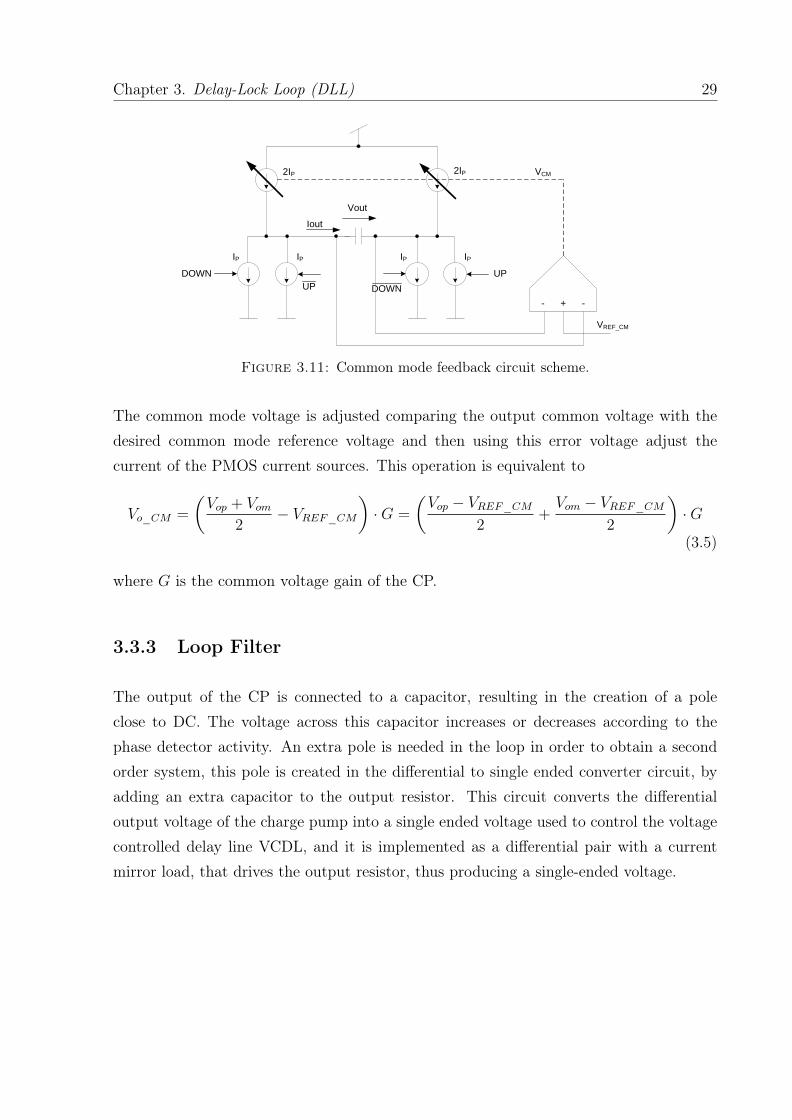
Figure 3.11: Common mode feedback circuit scheme.
The common mode voltage is adjusted comparing the output common voltage with thedesired common mode reference voltage and then using this error voltage adjust thecurrent of the PMOS current sources. This operation is equivalent to
Vo_CM =
(Vop + Vom
2− VREF_CM
)·G =
(Vop − VREF_CM
2+Vom − VREF_CM
2
)·G
(3.5)
where G is the common voltage gain of the CP.
3.3.3 Loop Filter
The output of the CP is connected to a capacitor, resulting in the creation of a poleclose to DC. The voltage across this capacitor increases or decreases according to thephase detector activity. An extra pole is needed in the loop in order to obtain a secondorder system, this pole is created in the differential to single ended converter circuit, byadding an extra capacitor to the output resistor. This circuit converts the differentialoutput voltage of the charge pump into a single ended voltage used to control the voltagecontrolled delay line VCDL, and it is implemented as a differential pair with a currentmirror load, that drives the output resistor, thus producing a single-ended voltage.

Chapter 3. Delay-Lock Loop (DLL) 30
3.3.4 Voltage Control Delay Line
The voltage controlled delay line (VCDL) must be able to produce a variable delay with amaximum value of 100 ns. Since only one delay element is unable to accomplish this task,a cascade of delay elements will be used. For a maximum delay value of 100 ns it will benecessary to use three variable delay elements followed by three fast buffers. The purposeof these last three buffers is to recover the rise and fall times of the clock signal afterthe delay is introduced. The delay of this delay line is three times the delay of a singlevariable delay buffer plus the delay of the fast buffer at the output. The architecture isdepicted in Fig. 3.12.
Replica Bias
Variable Delay
Replica BiasVBias_N variable VBias_N
VBias_P
VINVOUT
Figure 3.12: Architecture of the voltage controlled delay line (VCDL).
Chapter 4
Design and Simulation Results
4.1 Differential Buffer
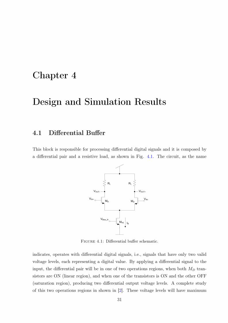
This block is responsible for processing differential digital signals and it is composed bya differential pair and a resistive load, as shown in Fig. 4.1. The circuit, as the name
VIN+ VIN-
VBias_N
MN1
MD MD
RL RL
VOUT+VOUT-
IB
Figure 4.1: Differential buffer schematic.
indicates, operates with differential digital signals, i.e., signals that have only two validvoltage levels, each representing a digital value. By applying a differential signal to theinput, the differential pair will be in one of two operations regions, when both MD tran-sistors are ON (linear region), and when one of the transistors is ON and the other OFF(saturation region), producing two differential output voltage levels. A complete studyof this two operations regions in shown in [2]. These voltage levels will have maximum
31
Chapter 4. Design and Simulation Results 32
value amplitude limited by the power supply (VDD), the Vdsat voltage of the transistorMN1 and a safety margin voltage (Vtol)(approx. 120 mV) to guaranty that transistor MN1
is in the saturation region. The output voltage swing (Vswing) is determined by the bufferbias current (IB) and by the load resistance value (RL) , using Ohm´s law
Vswing = RL × IB (4.1)
For the case of a bias current value of 100 µA and in order to obtain a voltage swing of400 mV at the output, results in RL = 4 KΩ. A voltage swing of 400 mV requires that
VDD − Vdsat(MN1)− Vtol ≥ Vswing (4.2)
whereVdsat(MN1) ≤ 680mV (4.3)
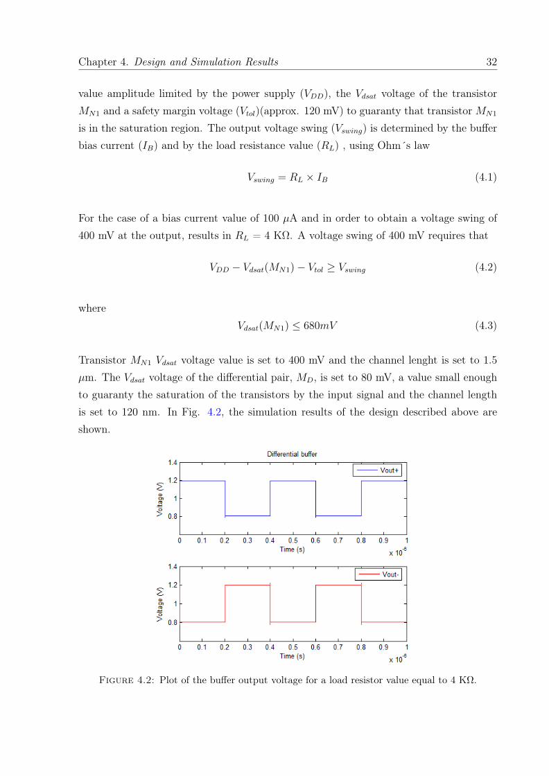
Transistor MN1 Vdsat voltage value is set to 400 mV and the channel lenght is set to 1.5µm. The Vdsat voltage of the differential pair, MD, is set to 80 mV, a value small enoughto guaranty the saturation of the transistors by the input signal and the channel lengthis set to 120 nm. In Fig. 4.2, the simulation results of the design described above areshown.
Figure 4.2: Plot of the buffer output voltage for a load resistor value equal to 4 KΩ.
Chapter 4. Design and Simulation Results 33
Vdsat (mV) L(µm) W(µm)MD 80 0.12 7.5MN1 400 1.5 3.7
Table 4.1: Buffer design summary for a bias current equal to 100 µA.
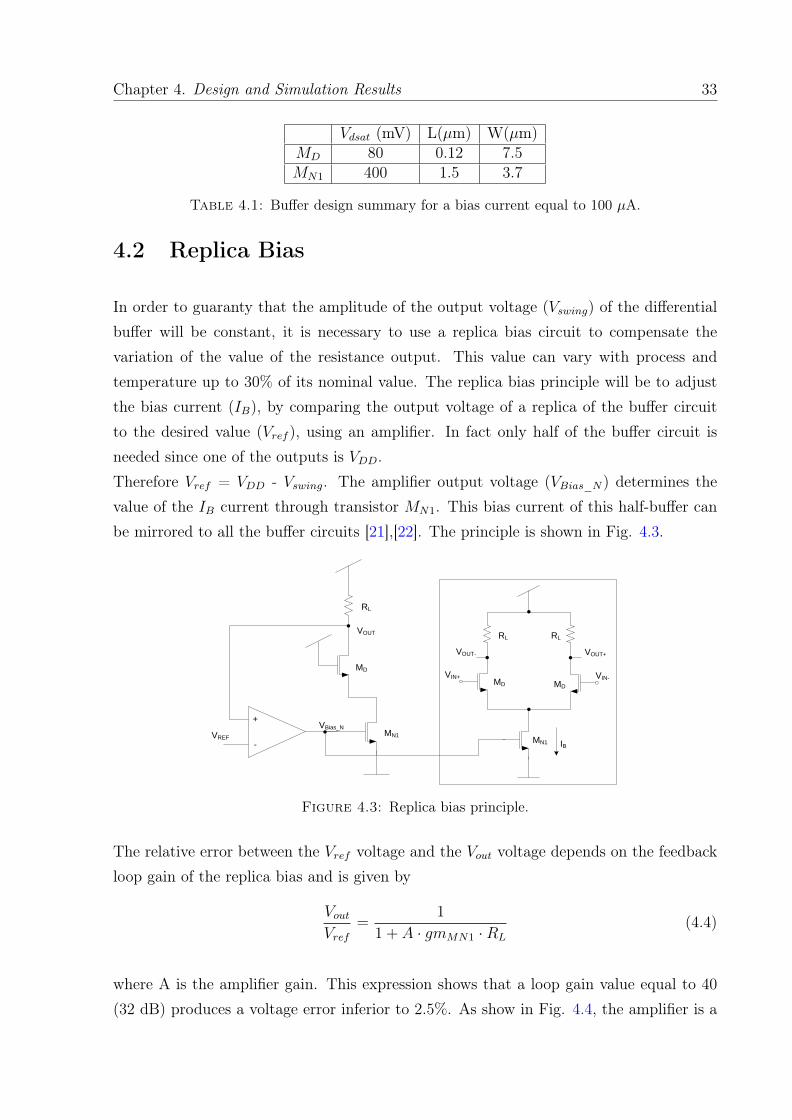
4.2 Replica Bias
In order to guaranty that the amplitude of the output voltage (Vswing) of the differentialbuffer will be constant, it is necessary to use a replica bias circuit to compensate thevariation of the value of the resistance output. This value can vary with process andtemperature up to 30% of its nominal value. The replica bias principle will be to adjustthe bias current (IB), by comparing the output voltage of a replica of the buffer circuitto the desired value (Vref ), using an amplifier. In fact only half of the buffer circuit isneeded since one of the outputs is VDD.Therefore Vref = VDD - Vswing. The amplifier output voltage (VBias_N) determines thevalue of the IB current through transistor MN1. This bias current of this half-buffer canbe mirrored to all the buffer circuits [21],[22]. The principle is shown in Fig. 4.3.
VIN+ VIN-
MN1
MD MD
RL RL
VOUT+VOUT-
IB
VBias_NMN1
MD
RL
+
-VREF
VOUT
Figure 4.3: Replica bias principle.
The relative error between the Vref voltage and the Vout voltage depends on the feedbackloop gain of the replica bias and is given by
VoutVref
=1
1 + A · gmMN1 ·RL
(4.4)
where A is the amplifier gain. This expression shows that a loop gain value equal to 40(32 dB) produces a voltage error inferior to 2.5%. As show in Fig. 4.4, the amplifier is a

Chapter 4. Design and Simulation Results 34
single stage amplifier because using a low loop gain value (within the limits of the gainspecification) improves the phase margin of the loop.
IBias
MN1_RB MN1_RBMN1_RB
MP1_RBMP1_RBMP1_RB
MD_RB MD_RB
VREF
CC
RCMD
RL
MN1
VBias_NN3
N1
N2N5
IB
N4
Figure 4.4: Replica bias circuit schematic.
The loop gain is given by
Gloop ≈gmD_RB · gmN1 ·RL
gdsP1_RB + gdsN1_RB(4.5)
As show in Fig. 4.4 the loop has a total of 5 poles, these are associated to the 5 nodes ofthe circuit in the signal path (N1 to N5). The dominant pole of the loop is located, bydesign, at node N3, its approximate expression can be obtained using Miller theorem andis given by
p3 ≈gdsP1_RB + gdsN1_RB
CC · (1 + gmN1 ·RL)(4.6)
The gain bandwidth product (GBW) is given by (assuming a phase margin larger than60)
GBW = p3 ·Gloop ≈gmD_RB
CC(4.7)
The phase margin of the loop is determined by all the 5 poles of the circuit and by the2 zeros, one zero created by the Cgs capacitance in the differential pair formed by theMD_RB transistors and the other zero is associated to the compensation resistor RC . Thephase margin is the difference between 180and the phase gain at the GBW frequency

Chapter 4. Design and Simulation Results 35
and is calculated using
PM = 180 −[∑
arctan(GBW
−pi)−
∑arctan(
GBW
−zi)
](4.8)
The remaining poles are given by
p1 ≈−2 · gmD_RB
2 · CgsD_RB + Cp1(4.9)
p2 ≈−gmP1_RB
2 · CgsP1_RB + Cp2(4.10)
p4 ≈−gmD
2 · CgsD + Cp4(4.11)
p5 ≈−gmN1 · CC
Cp3 · Cp5 + CC · Cp3 + CC · Cp5(4.12)
The value of Cp5 is small compared to the Cp3 value, it is approximately equal to Cp3 ≈M · CgsN1, since the transistors inside the buffers controlled by the replica bias have thesame Vdsat voltages as the transistors of the half buffer. Under these condition the p5expression can be further simplified to
p5 ≈Vdsat_N1
M · L2N1
·K (4.13)
where K is technology dependent parameter.As in any feedback loop, the replica bias amplifier must be designed to assure that theloop is unconditionally stable. Therefore the specifications for this circuit are a loop gainlarger than 32 dB, since the control voltage VBias_N is essentially a DC signal, a GBWlarger than 100 kHz is enough, and phase margin larger than 60.Inside the half-buffer the transistors have the same Vdsat voltages and channel lengthsas the transistors inside the differential buffer. To reduce the parasitic capacitance thechannel length of transistors MD_RB should be small, therefore a value of 0.5 µm anda Vdsat value of 100 mV are defined to obtain the largest possible gain and GBW valuesfor a given current value. The Vdsat values for the transistors MN1_RB and MP1_RB areselected to be 300 mV to reduce the parasitic capacitance. The channel length ofMN1_RB

Chapter 4. Design and Simulation Results 36
is set to 2 µm to improve the gain and for the MP1_RB is set to 2 µm. The values of theresistance and capacitor are selected together using AC simulations resulting in CC = 3ρF and RC = 4 kΩ. After the previous design process the circuit design goals were obtainand are shown next in table 4.2.
Design Typical SimulationGoals Results
Gain(dB) 32 44.2GBW(MHz) 0.1 16.7Phase() 60 81.5
Table 4.2: Replica bias simulation results.
Since the simulations results can vary with temperature and supply voltage values, acorners analysis was made to assure that the loop is unconditionally stable.
Supply Voltage (V) Section Temperature (C) Gain (dB) GWB (MHz) PM ()
Vdd = 1.2Slow 0 42.9 19.4 73.1
80 40.6 14.9 65.4
Fast 0 45.8 17.2 98.380 44.5 13.6 86.8
Vdd = 1.08Slow 0 41.4 18.0 69.1
80 39.1 13.7 61.9
Fast 0 44.0 16.1 92.880 42.0 12.6 80.8
Vdd = 1.3Slow 0 43.8 20.1 75.5
80 41.5 15.3 67.7
Fast 0 46.6 17.8 100.980 45.6 14.1 90.3
Table 4.3: Corners analysis simulation results confirming the stability of the loop.
This results showed that the circuit design parameters are well adjusted and the loop isunconditionally stable.
Vdsat(mV) L(µm) W(µm)MD_RB 100 0.5 10MN1_RB 300 2 8.8MP1_RB 300 2 20
Table 4.4: Replica bias design summary.

Chapter 4. Design and Simulation Results 37
4.3 Differential Buffer with Variable Delay
This circuit is used in the voltage controlled delay line (VCDL) to help produce a maximumvalue of 100 µs to accomplish the radar system specifications. The differential buffer inFig. 4.1 can produce a variable delay [9], by changing the load resistance of the bufferusing MOS transistors in the linear region. The differential buffer circuit with symmetricloads [9] is show in Fig. 4.5.
VIN+ VIN-
VBias_N
MN1
MD MD
MP1MP2
VOUT+VOUT-
IB
CVBias_P
MP1MP2
VBias_PC
Figure 4.5: Schematic of the differential buffer with symmetric loads.
A PMOS transistor is in the linear region when VSD < VSG − |VT |, when this conditionapplies the drain current is given by
ID = β ·[(VSG − |VT |) · VSD −
V 2SD
2
](4.14)
where β = Kp · WL and Kp is the transistor transconductance which depends on thetechnology and varies with process and temperature. The drain resistance of the transistoris calculated using
rsd =
(dIDdVSD
)−1
=1
β · [(VSG − |VT |)− VSD](4.15)
The expression shows that the resulting resistor has a non-linear dependence on the VSDvoltage. The VSG voltage should be as large as possible, compared to the maximum VSD
voltage, to reduce this non-linear behavior and to guaranty that the transistor is in the

Chapter 4. Design and Simulation Results 38
linear region.The drain current of the MP1 transistor is given by
ID = β ·[(VSD
2− |VT |)
]· VSD (4.16)
The drain resistance of MP2 transistor is given by expression 4.15 and for MP1 transistoris calculated using
rsd =
(dIDdVSD
)−1
=1
β · (VSD − |VT |)(4.17)
From expressions 4.15 and 4.17 it is possible to calculate the equivalent resistance fromthe symmetrical load resulting in
rsdeq. =1
β · (VDD − VBias_P − 2 · |VT |)(4.18)
The bias current of this circuit can be calculated using expression 4.14 and expression4.16 resulting in
IB ≈β
2· (VDD − VBias_P − VT )2 +
β
2· (Vswing − VT )2 (4.19)
This equation shows that the current in the buffer changes quadratically with both thecontrol voltage (VBias_P ) and the clock signal amplitude (Vswing).If both PMOS transistors, in the symmetrical load, have the same size, this type of loadexhibits an almost constant conductance, when the output voltage changes. The delay ofeach differential stage varies with the value of the load conductance, which can be adjustedusing the control voltage VBias_P . The delay of the differential buffer is proportional tothe RC time constant of the output node and it can be calculated [2] using :
TD(VBias_P ) ≈ 0.7× Cβ · [(VDD − VBias_P − 2 · |VT |)]
(4.20)
From this expression it is clear that the delay depends only on the β, C and VBias_P
values and only this last one can be used to vary the delay. The minimum delay isobtained when the VBias_P is equal to 0 volt (VSG = VDD) and the maximum delay isobtained when VBias_P = VDD − |VT | − Vswing (VSG = Vswing + |VT |) corresponding to theonset of saturation region in the PMOS transistor.
Chapter 4. Design and Simulation Results 39
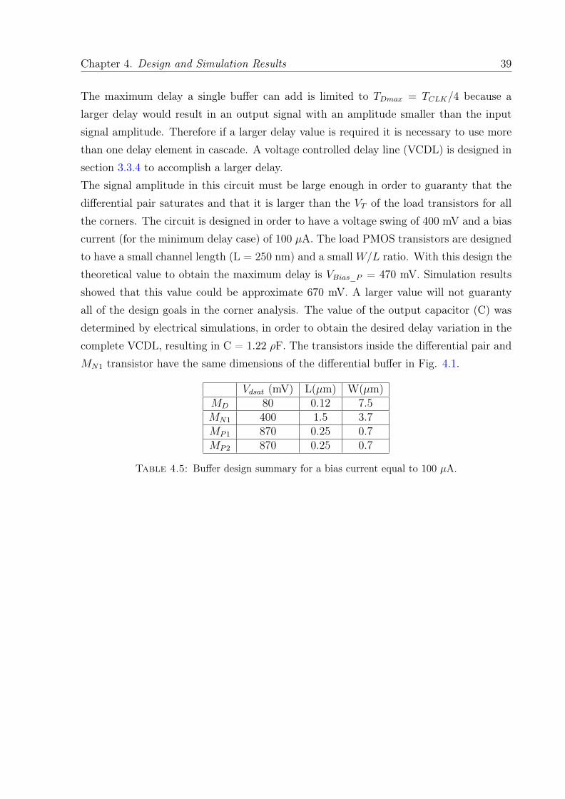
The maximum delay a single buffer can add is limited to TDmax = TCLK/4 because alarger delay would result in an output signal with an amplitude smaller than the inputsignal amplitude. Therefore if a larger delay value is required it is necessary to use morethan one delay element in cascade. A voltage controlled delay line (VCDL) is designed insection 3.3.4 to accomplish a larger delay.The signal amplitude in this circuit must be large enough in order to guaranty that thedifferential pair saturates and that it is larger than the VT of the load transistors for allthe corners. The circuit is designed in order to have a voltage swing of 400 mV and a biascurrent (for the minimum delay case) of 100 µA. The load PMOS transistors are designedto have a small channel length (L = 250 nm) and a smallW/L ratio. With this design thetheoretical value to obtain the maximum delay is VBias_P = 470 mV. Simulation resultsshowed that this value could be approximate 670 mV. A larger value will not guarantyall of the design goals in the corner analysis. The value of the output capacitor (C) wasdetermined by electrical simulations, in order to obtain the desired delay variation in thecomplete VCDL, resulting in C = 1.22 ρF. The transistors inside the differential pair andMN1 transistor have the same dimensions of the differential buffer in Fig. 4.1.
Vdsat (mV) L(µm) W(µm)MD 80 0.12 7.5MN1 400 1.5 3.7MP1 870 0.25 0.7MP2 870 0.25 0.7
Table 4.5: Buffer design summary for a bias current equal to 100 µA.
Chapter 4. Design and Simulation Results 40
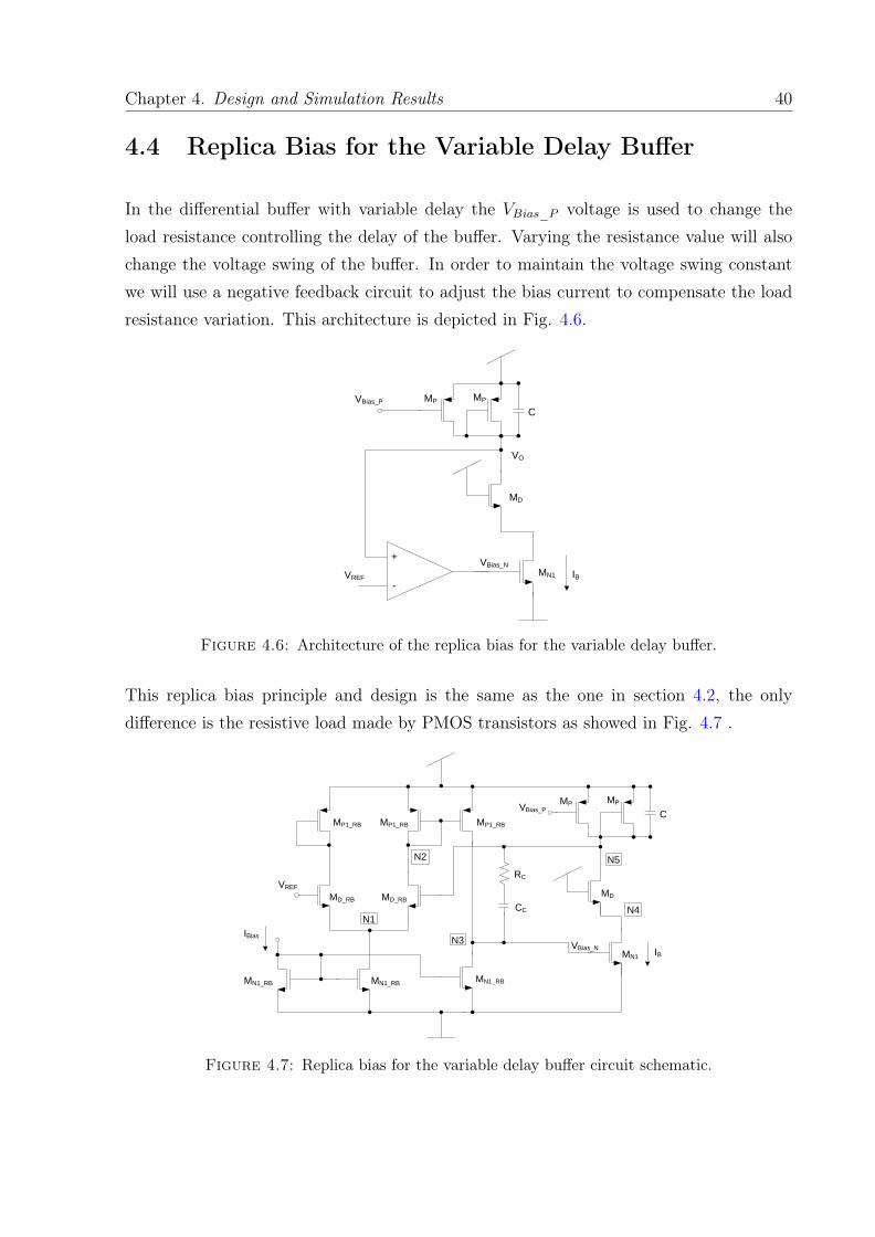
4.4 Replica Bias for the Variable Delay Buffer
In the differential buffer with variable delay the VBias_P voltage is used to change theload resistance controlling the delay of the buffer. Varying the resistance value will alsochange the voltage swing of the buffer. In order to maintain the voltage swing constantwe will use a negative feedback circuit to adjust the bias current to compensate the loadresistance variation. This architecture is depicted in Fig. 4.6.
VBias_N
MN1
MD
+
-VREF
VO
MPMP
C
VBias_P
IB
Figure 4.6: Architecture of the replica bias for the variable delay buffer.
This replica bias principle and design is the same as the one in section 4.2, the onlydifference is the resistive load made by PMOS transistors as showed in Fig. 4.7 .
IBias
MN1_RB MN1_RBMN1_RB
MP1_RBMP1_RBMP1_RB
MD_RB MD_RB
VREF
CC
RC
VBias_NN3
N1
N2
MD
MN1
N5
IB
N4
MPMP
CVBias_P
Figure 4.7: Replica bias for the variable delay buffer circuit schematic.

Chapter 4. Design and Simulation Results 41
The replica bias circuit is designed to have a bandwidth larger than the clock frequencyof the circuit (in order not to introduce any extra poles into the circuit) and in order tobe stable for all the possible values of the control voltage VBias_P . If a clock frequencyof 2 MHz is used, then the replica bias should have a loop bandwidth of at least 8 MHz.Inside the half-buffer the transistors have the same Vdsat voltages and channel lengths asthe transistors inside the differential buffer with variable delay. The transistors MD_RB
inside the differential pair will have a Vdsat inferior to the ones in section 4.2 to increase theloop gain. The values of the resistance and capacitor will be selected together using ACsimulations resulting in CC = 3.5 ρF and RC = 13.5 kΩ. DC and AC simulations weremade considering the maximum and minimum values for VBias_P . Results are showednext in table 4.6.
Design Goals Simulation Results Simulation Results(VBias_P = 0 V) (VBias_P = 650 mV)
Gain(dB) 32 48.28 43.76GBW(MHz) 8 17.2 18.1Phase() 60 69.7 81.6
Table 4.6: Replica bias for the variable delay buffer simulation results.
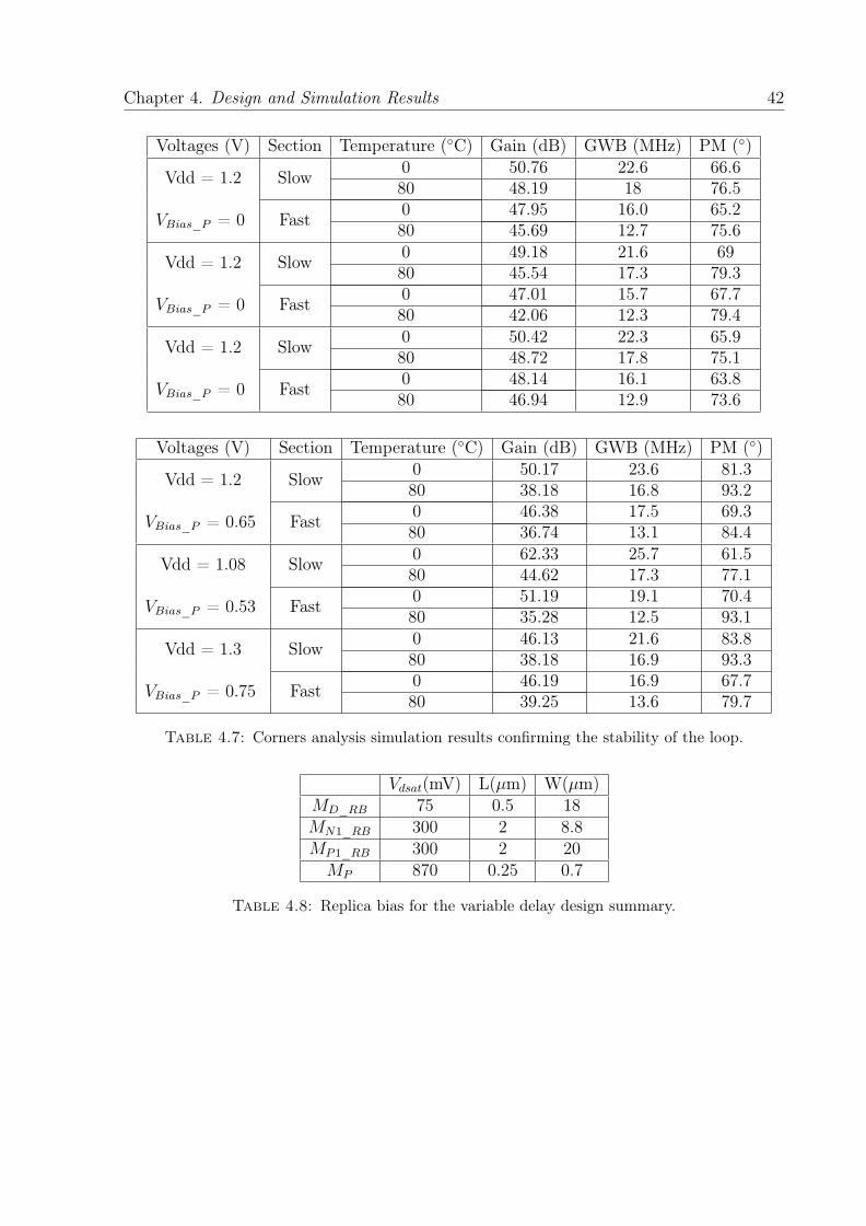
Since the simulations results can vary with temperature, supply voltage and in this casethe VBias_P voltage values, a corners analysis was made to assure that the loop is uncon-ditionally stable. The results are showed in the next page.
Chapter 4. Design and Simulation Results 42
Voltages (V) Section Temperature (C) Gain (dB) GWB (MHz) PM ()
Vdd = 1.2 Slow 0 50.76 22.6 66.680 48.19 18 76.5
VBias_P = 0 Fast 0 47.95 16.0 65.280 45.69 12.7 75.6
Vdd = 1.2 Slow 0 49.18 21.6 6980 45.54 17.3 79.3
VBias_P = 0 Fast 0 47.01 15.7 67.780 42.06 12.3 79.4
Vdd = 1.2 Slow 0 50.42 22.3 65.980 48.72 17.8 75.1
VBias_P = 0 Fast 0 48.14 16.1 63.880 46.94 12.9 73.6
Voltages (V) Section Temperature (C) Gain (dB) GWB (MHz) PM ()
Vdd = 1.2 Slow 0 50.17 23.6 81.380 38.18 16.8 93.2
VBias_P = 0.65 Fast 0 46.38 17.5 69.380 36.74 13.1 84.4
Vdd = 1.08 Slow 0 62.33 25.7 61.580 44.62 17.3 77.1
VBias_P = 0.53 Fast 0 51.19 19.1 70.480 35.28 12.5 93.1
Vdd = 1.3 Slow 0 46.13 21.6 83.880 38.18 16.9 93.3
VBias_P = 0.75 Fast 0 46.19 16.9 67.780 39.25 13.6 79.7
Table 4.7: Corners analysis simulation results confirming the stability of the loop.
Vdsat(mV) L(µm) W(µm)MD_RB 75 0.5 18MN1_RB 300 2 8.8MP1_RB 300 2 20MP 870 0.25 0.7
Table 4.8: Replica bias for the variable delay design summary.

Chapter 4. Design and Simulation Results 43
4.5 Voltage Controlled Delay Line
After the design of the circuits described in the previous sections, its possible to accomplishthe architecture of the VCDL in Fig. 3.12. The delay of the VCDL as a function of thecontrol voltage, was simulated for different process corners, the result is shown in Fig.4.8.
Figure 4.8: Simulated delay of the VCDL as a function of the control voltage.
This graphic shows that for a control voltage (VBias_P ) of ≈ 650 mV the delay line canproduce a delay of 100 ns and for a VBias_P voltage value of 0 V, a minimum delay of 18.7ns.The gain factor of the VCDL (KV CDL) is given by the derivative of the delay to the controlvoltage (VBias_P ), this is inversely proportional to the square of the control voltage:
KV CDL =
(dTD
dVBias_P
)∝ 1
V 2Bias_P
(4.21)
This gain can be obtained by numerically calculating the derivative of the delay of VCDL(obtained by electrical simulation Fig. 4.8). The value of the KV CDL as a function of thecontrol voltage is showned in Fig. 4.9.

Chapter 4. Design and Simulation Results 44
Figure 4.9: Simulated gain curve of the VCDL.
As expected, this graph shows that (KV CDL) increases quadratically with the controlvoltage. This means that the loop gain of the DLL will increase quadratically with thedesired delay. This is a problem, because it means that the DLL closed loop pole frequencyand quality factor will change significantly with the delay (as shown by expressions 3.3and 3.4). The end result is that for larger delays, the KV CDL value is very large whichmeans that the closed loop pole frequency increases (the quality factor also) and thereforethe jitter noise at the output of the DLL will also increase. In order to maintain a smalljitter noise at the output of the DLL it would be necessary to use a charge pump current(IP ) value that can produce a compromise between the jitter power for large delays andthe DLL response time for small delays. This results in a value of IP equal to 5 µA. Thissubject will be further address in the charge pump design section.
Chapter 4. Design and Simulation Results 45
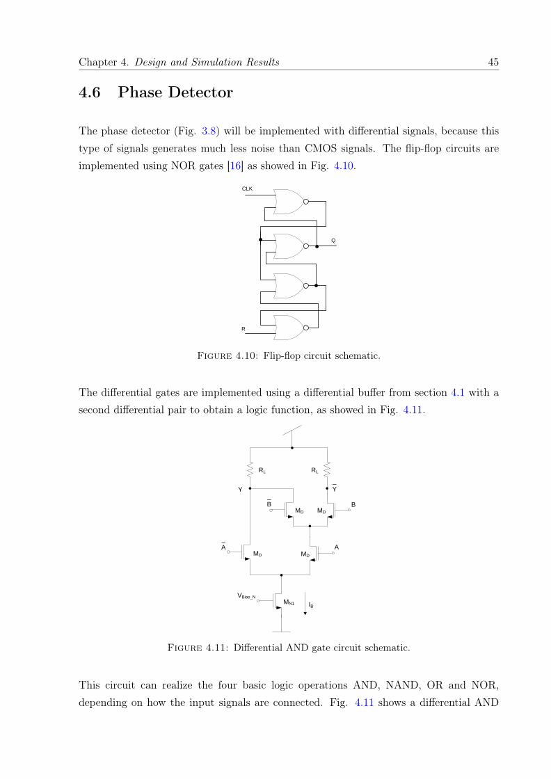
4.6 Phase Detector
The phase detector (Fig. 3.8) will be implemented with differential signals, because thistype of signals generates much less noise than CMOS signals. The flip-flop circuits areimplemented using NOR gates [16] as showed in Fig. 4.10.
CLK
R
Q
Figure 4.10: Flip-flop circuit schematic.
The differential gates are implemented using a differential buffer from section 4.1 with asecond differential pair to obtain a logic function, as showed in Fig. 4.11.
_
A A
VBias_N
MN1
MD MD
RL RL
Y
IB
BMD
_
BMD
_
Y
Figure 4.11: Differential AND gate circuit schematic.
This circuit can realize the four basic logic operations AND, NAND, OR and NOR,depending on how the input signals are connected. Fig. 4.11 shows a differential AND

Chapter 4. Design and Simulation Results 46
gate, reversing the polarity of both input signals, would change the circuit into a ORgate. Realizing a NOT function using differential signals consists simply in inverting theoutput signals. This way we achieve the NAND and NOR gates. The truth table of thedifferential AND gate is shown in table 4.9. The design of the differential gates are equalto the differential buffer from section 4.1 (see table 4.1).
Differential A Differential B A A B B Y Y Differential Y0 0 0 1 0 1 0 1 01 0 1 0 0 1 0 1 00 1 0 1 1 0 0 1 01 1 1 0 1 0 1 0 1
Table 4.9: Truth table of the differential AND gate.
4.7 Charge Pump
In section 3.3.2 a brief introduction to the architecture of the CP was done. The mainproblem with a differential charge pump is the fact that it haves a lower output resistancemade by the constant connection of the current sources to output node. The CP usesa folded cascode topology to increase the output resistance and maintain a large outputvoltage swing for a low power supply. Since the CP is completely differential the outputresistance should be maximized through a careful design of the current source circuitsinside the CP. This circuit is depicted in Fig. 4.12.
VUP-
MN1
MD MD
IP
VDOWN-
MN1
MD MD
IP
OUT+
VBias_N1
VBias_N2
VBias_P2
VB_CM
OUT-
VBias_N2
VBias_P2
VB_CM
MN1
MN2 MN2
MN1
MP2 MP2
MP1 MP12IP2.IP;IP;0
-IP;0;IP
VUP+ VDOWN+
VBias_N1 VBias_N1 VBias_N1
Figure 4.12: Folded cascode charge pump circuit schematic.

Chapter 4. Design and Simulation Results 47
The transistors MP1 produce a current equal to 2.IP and the transistors MN1 produce acurrent equal to IP . This current will charge a capacitor (C1) increasing or decreasing itsvoltage depending on which current source is on. The output current is determined bythe two differential pairs that act as switches steering the current produced by the MP1
transistors from the output branch. Transistors MP2 and MN2 act as cascode devices andincrease the output resistance of the current source transistors. The output resistance ofthe charge pump is given by [2]
Rout =RN ·RP
RN +RP
(4.22)
where
RP ≈1
gdsP1 + gdsND· gmP2
gdsP2
(4.23)
andRN ≈
1
gdsN1
· gmN2
gdsN2
(4.24)
The maximum differential output voltage of the CP is given by
Vswing_CP = VDD − Vdsat_P1 − Vdsat_P2 − Vdsat_N2 − Vdsat_N1 − Vtol (4.25)
where Vtol is the safety margin to guaranty that all the transistors are well into thesaturation region (approx. 120 mV).
Since the operation of the CP depends on the common mode comparator (see Fig. 3.11),both this circuits must be design together in order to guaranty that the common modefeedback loop is stable. Expression 3.5 suggest that the common mode comparator cir-cuit can be implemented using two differential pairs, each comparing the common modereference voltage (VREF_CM) with one of the output voltages [2]. The common modecomparator circuit is depicted in Fig. 4.13.

Chapter 4. Design and Simulation Results 48
VIN+
VBias_N1 MN1cm
MDcm MDcm
VIN-
VBias_N1 MN1cm
MDcm MDcm
IP IP
MP1cm MP1cm
VB_CM
VREF_CM
Figure 4.13: Common mode comparator circuit.
The differential pairs have an output current proportional to the difference between thepositive or negative output voltage and the desired common mode voltage level. Thecurrents produced by this differential pairs are summed in the transistor MP1, generatinga bias voltage for the transistor MP1 inside the charge pump circuit (these transistorsshould have the same channel length and Vdsat voltage). If the differential pairs saturatethe common mode circuit will stop adjusting the output common voltage (VB_CM), so inorder to prevent this it is required that
Vswing_CP <√
2 · Vdsat_Dcm (4.26)
The minimum value of the desired common mode voltage is also limited by the minimuminput common mode voltage of the differential pairs and is given by
VCM ≥ VT + Vdsat_Dcm + Vdsat_N1cm (4.27)
From the small signal analysis of this loop in [2], the common mode loop gain expressionresults in
G ≈ 2× gmDcm ·Rout (4.28)
Chapter 4. Design and Simulation Results 49
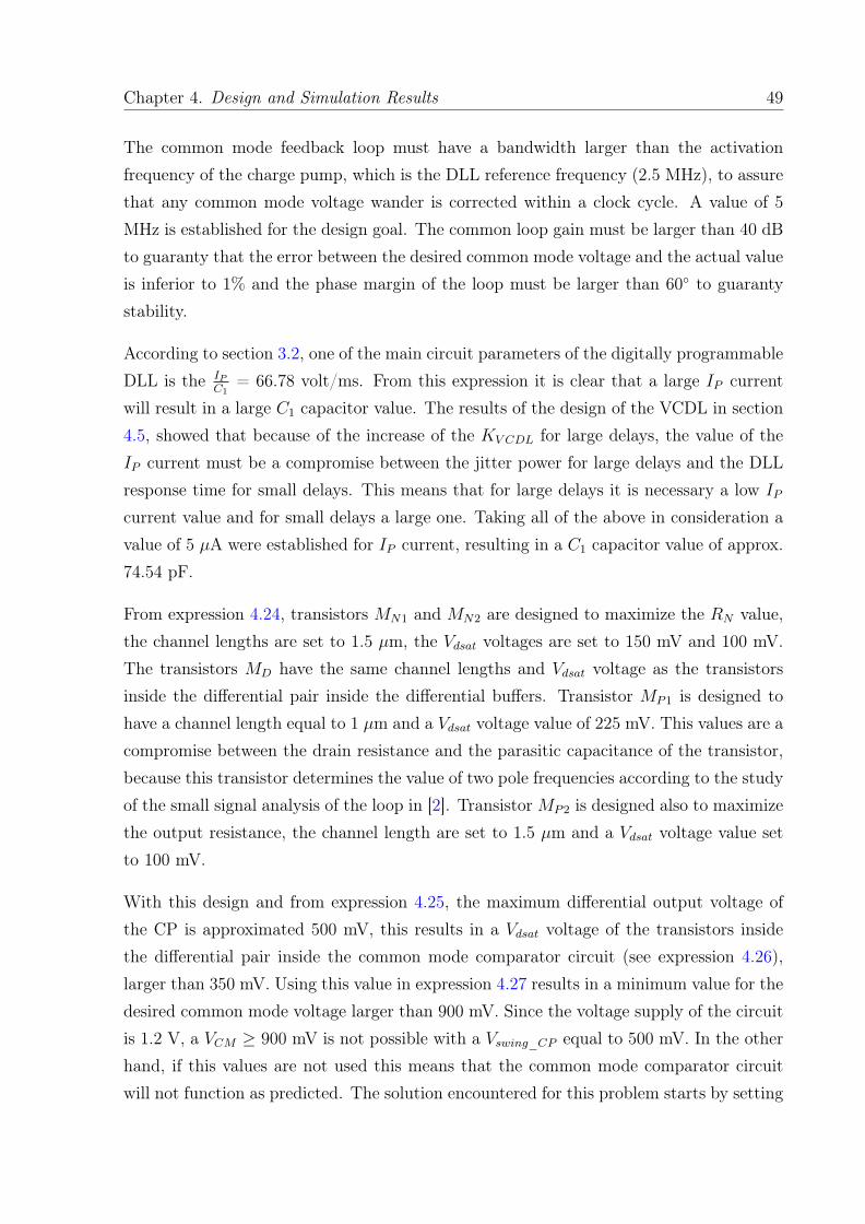
The common mode feedback loop must have a bandwidth larger than the activationfrequency of the charge pump, which is the DLL reference frequency (2.5 MHz), to assurethat any common mode voltage wander is corrected within a clock cycle. A value of 5MHz is established for the design goal. The common loop gain must be larger than 40 dBto guaranty that the error between the desired common mode voltage and the actual valueis inferior to 1% and the phase margin of the loop must be larger than 60 to guarantystability.
According to section 3.2, one of the main circuit parameters of the digitally programmableDLL is the IP
C1= 66.78 volt/ms. From this expression it is clear that a large IP current
will result in a large C1 capacitor value. The results of the design of the VCDL in section4.5, showed that because of the increase of the KV CDL for large delays, the value of theIP current must be a compromise between the jitter power for large delays and the DLLresponse time for small delays. This means that for large delays it is necessary a low IP
current value and for small delays a large one. Taking all of the above in consideration avalue of 5 µA were established for IP current, resulting in a C1 capacitor value of approx.74.54 pF.
From expression 4.24, transistors MN1 and MN2 are designed to maximize the RN value,the channel lengths are set to 1.5 µm, the Vdsat voltages are set to 150 mV and 100 mV.The transistors MD have the same channel lengths and Vdsat voltage as the transistorsinside the differential pair inside the differential buffers. Transistor MP1 is designed tohave a channel length equal to 1 µm and a Vdsat voltage value of 225 mV. This values are acompromise between the drain resistance and the parasitic capacitance of the transistor,because this transistor determines the value of two pole frequencies according to the studyof the small signal analysis of the loop in [2]. TransistorMP2 is designed also to maximizethe output resistance, the channel length are set to 1.5 µm and a Vdsat voltage value setto 100 mV.
With this design and from expression 4.25, the maximum differential output voltage ofthe CP is approximated 500 mV, this results in a Vdsat voltage of the transistors insidethe differential pair inside the common mode comparator circuit (see expression 4.26),larger than 350 mV. Using this value in expression 4.27 results in a minimum value for thedesired common mode voltage larger than 900 mV. Since the voltage supply of the circuitis 1.2 V, a VCM ≥ 900 mV is not possible with a Vswing_CP equal to 500 mV. In the otherhand, if this values are not used this means that the common mode comparator circuitwill not function as predicted. The solution encountered for this problem starts by setting
Chapter 4. Design and Simulation Results 50
the VCM value to 500 mV, resulting in a low Vdsat voltage value for the MDcm transistors,which at one point will make the transistors inside the differential pair saturate and thecommon mode voltage will stop being adjust. Simulation results showed that this willnot affect the functionality of the DLL (with a careful design of transistors MDcm) sincewhen the comparator stops adjusting the common mode voltage will maintain stable atapproximate value of 500 mV.
Inside the common mode comparator circuit, transistors MP1cm and transistors MN1cm
are designed with the same channel length and Vdsat voltage as the equivalent transistorsinside the charge pump. Since transistors MN1cm will have 2.IP the size relation must bemultiplied by 2. Transistors MDcm channel length are set to 1.2 µm and the Vdsat voltageare set with a low value. This transistor size relation W/L is adjusted by simulationsresults.
After the previous describe design process the circuit design parameters were obtain andare showed next in table 4.10.
Design Typical SimulationGoals Results
Gain(dB) 40 74.87GBW(MHz) 5 6.89Phase() 60 82.90Rout(MΩ) ∞ 63.18
Table 4.10: Charge pump simulation results.
Since the simulations results can vary with temperature, supply voltage values, a cornersanalysis was made to assure that the loop is unconditionally stable.

Chapter 4. Design and Simulation Results 51
Supply Voltage (V) Section Temp.(C) Gain (dB) GWB (MHz) PM () Rout(MΩ)
Vdd = 1.2Slow 0 74.70 7.70 81.9 64.77
80 69.60 6.92 82.0 39.88
Fast 0 76.28 6.58 83.74 68.1280 72.50 5.79 83.88 49.77
Vdd = 1.08Slow 0 74.70 7.70 81.93 54.42
80 69.60 6.92 82.06 32.06
Fast 0 76.28 6.58 83.74 61.6080 72.50 5.79 83.88 44.07
Vdd = 1.3Slow 0 74.70 7.70 81.93 67.26
80 69.60 6.92 82.06 39.25
Fast 0 76.28 6.58 83.74 70.4780 72.50 5.79 83.88 49.79
Table 4.11: Corners analysis simulation results confirming the stability of the loop.
This results showed that the circuit design parameters are well adjusted and the loop isunconditionally stable.
Vdsat(mV) L(µm) W(µm)MD 80 0.12 7.5MN1 150 1.5 1.3MN2 100 1.5 3MP1 225 1 4MP2 100 1.5 15
Table 4.12: Charge pump design summary.
Vdsat(mV) L(µm) W(µm)MDcm 80 1.2 4.8MN1cm 150 1.5 2.7MP1cm 225 1 4
Table 4.13: Common mode comparator design summary.
Chapter 4. Design and Simulation Results 52
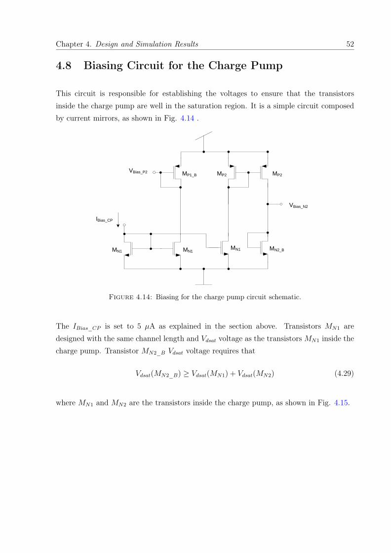
4.8 Biasing Circuit for the Charge Pump
This circuit is responsible for establishing the voltages to ensure that the transistorsinside the charge pump are well in the saturation region. It is a simple circuit composedby current mirrors, as shown in Fig. 4.14 .
IBias_CP
MN1 MN1MN1 MN2_B
MP2MP2MP1_B
VBias_N2
VBias_P2
Figure 4.14: Biasing for the charge pump circuit schematic.
The IBias_CP is set to 5 µA as explained in the section above. Transistors MN1 aredesigned with the same channel length and Vdsat voltage as the transistors MN1 inside thecharge pump. Transistor MN2_B Vdsat voltage requires that
Vdsat(MN2_B) ≥ Vdsat(MN1) + Vdsat(MN2) (4.29)
where MN1 and MN2 are the transistors inside the charge pump, as shown in Fig. 4.15.

Chapter 4. Design and Simulation Results 53
MN2_B
VBias_N2
IP
VBias_N1 MN1
MN2
Charge PumpBias Circuit
Figure 4.15: Design of transistor MN2_B .
From the design of the charge pump, the Vdsat voltage value of transistor MN2_B must begreater than 250 mV. The value is set to 350 mV and the channel width is set to 1 µm.Transistors MP1_B channel width is set to 1 µm and the channel length is adjusted bysimulation results, resulting in a value equal to 1.5 µm. The channel length of transistorsMP2 is set to 1.2 µm and the Vdsat voltage value set to 150 mV.
Vdsat(mV) L(µm) W(µm)MN1 150 1.5 1.3MN2B 350 6.1 1MP1B ≈ 375 1.5 1MP2 150 1.2 5.3
Table 4.14: Biasing circuit design summary.

Chapter 4. Design and Simulation Results 54
4.9 Differential to Single Ended Signal Converter
This circuit is responsible for creating an extra pole in the loop in order to obtain a secondorder system and for converting the differential output voltage of the charge pump into asingle ended voltage, used to control the voltage controlled delay line (VCDL). The circuitwill also provide some gain into the loop and is depicted in the Fig. 4.16 below.
MN1
MP1_2MP1MP1
MD MD
VCP+VCP-
IB
IBias_dse
MN1R2 C2
VBias_P
Figure 4.16: Differential to single ended conversion circuit and second pole.
The output resistor (R2) together with the capacitor (C2) implements the time constant(τRC) necessary to create the second pole of the DLL loop. The DLL clock frequency is2.5 MHz, so the second pole frequency must be much smaller than this value. The valueof the output resistance value is selected together with the output capacitance to obtainthe desired value of τRC and a small area. According to section 3.2, one of the main circuitparameters of the digitally programmable DLL is the τRC = 7.16 µs. The output resistorvalue is set to 150 KΩ resulting in a output capacitance value of 47.76 pF. With thisvalues, the second pole frequency value is 22.2 KHz. The bias current (IBias_dse) is set to2.5 µA. Transistors MD are designed with a large Vdsat voltage value of 300 mV and thechannel length are set to 1 µm. The Vdsat voltage value of transistors MN1 are set to 100mV and the channel length are set to 1.2 µm. Transistors MP1 and MP1_2 are designedwith a channel length of 1 µm and a Vdsat voltage value of 150 mV. Transistors MP1_2
will have 2.IB so the size relation must be multiplied by 2. This transistor was adjusted

Chapter 4. Design and Simulation Results 55
with the simulations of the DLL in order for the maximum delay of the VCDL (100 ns),the output voltage of the circuit is equal to 650 mV. After the simulations the maximumgain measured was equal to 2.8 .
Vdsat(mV) L(µm) W(µm)MD 300 1 9MN1 100 1.2 1.2MP1 150 1 2.2MP1_2 150 1 4.6
Table 4.15: Differential to single ended design summary.
4.10 Digitally Programmable DLL
All of the constituting blocks of the DLL were designed in the sections above. Thissection will show how the simulations of the digitally programmable DLL were made andthe respective results. The architecture of the circuit is shown again in Fig. 3.2.
ΣΔ
DLL
Master clock
Delay
TD
Reference
clockOutput clock
Figure 4.17: Architecture of the digitally programmable DLL.
The digital Σ∆ modulator controls the switching sequence that produces the referenceclock. This clock is created by selecting between the input clock and a delayed version ofthe input clock. The switches used to do this selection can add jitter and extra delay to theclock signals, due to the ON resistance and the parasitic capacitance. These switches areimplemented as CMOS switches as shown in Fig. 4.18. The transistors in these switchesmust be carefully designed in order to reduce the unwanted effects in the clock signals.The design parameters are shown in Table 4.16.

Chapter 4. Design and Simulation Results 56
Control_p
Control_p
Control_m
Delayed_clock
Master_clock
Reference_clock
MP
MP
MN
MN
Figure 4.18: CMOS switches circuit schematic.
L(µm) W(µm)MN 0.12 0.16MP 0.12 20
Table 4.16: CMOS switches design summary.
The Σ∆ modulator was simulated at high level for different input values and the resultingoutput bit stream was imported into the electrical simulator to control several voltagesources. This voltage sources are responsible for the master clock, the delayed clock andthe differential signal (Control_m and Control_p) used to switch between the masterclock and the delayed clock. The master clock frequency is 2.5 MHz, corresponding to aclock period of 400 ns. These signals were used to run electrical simulations of the circuitwith different delays, the resulting step responses of the programmable delay are shownnext in Fig. 4.19. The delay produced by the circuit as a function of the programmingdelay is shown in Fig. 4.20, and the simulated output jitter noise of the circuit for differentdelays is shown in Fig. 4.21.

Chapter 4. Design and Simulation Results 57
Figure 4.19: Simulated step response of the DLL. Programmable delay from 20 ns to99 ns.
Figure 4.20: Simulated output delay as a function of the programming delay.

Chapter 4. Design and Simulation Results 58
Figure 4.21: Jitter noise simulation results of the programmable DLL.
These simulation results shown that the DLL loop is stable for the different delays, butthe output jitter increases with the desired delay. The cause for this increase is due to theincrease of the gain factor of the VCDL (KV CDL) (see section 4.5). For the programmingdelay value of 99 ns the output jitter value is equal to 1199 ps.
In order to obtain a better performance it would be necessary to adjust the charge pumpcurrent, in order to compensate for the variation of the KV CDL. Noting that the biascurrent of the variable delay (given by expression 4.14) increases with the square of thecontrol voltage value (VBias_P ) and that the KV CDL value decreases with the square of thecontrol voltage (expression 4.21), it is clear that the product of these two variables can beindependent of the control voltage (in a first order approach). Therefore the charge pumpcurrent value is determined according to the value of the bias current of the variable delaybuffer. This is achieved by adjusting the bias current of the charge-pump circuit usingthe circuit in Fig. 4.22.

Chapter 4. Design and Simulation Results 59
Charge Pump
Replica Bias
Variable Delay
IB_CP
Variable
IB_CP
Figure 4.22: Architecture of variable charge pump current.
The previous circuit has a fixed bias current (IB_CP value of 1.67 A, the variable biascurrent will change between approx. 6.5 µA (for a delay of 20 ns) and approx. 185 nA(for a delay of 99 ns). Since the charge pump current as a large variation, the closed loopfrequency pole (fp) value and the quality factor (Qp) will also change. This values are veryimportant since they are responsible for the system resolution (see section 3.2). Simulationresults of the DLL discrete function (Eq. 3.2) with the maximum and minimum chargepump current values are shown in Table 4.17.
Charge Pump Current (µA) fp (KHz) Qp Resolution (bits)0.185 3.07 0.138 146.5 18.24 0.791 8.8
Table 4.17: Closed loop frequency pole (fp) and quality factor (Qp) simulations resultswith variable charge pump current.
From section 3.2, the programming resolution must be equal to 9 bits. This simulationsresults shows that for the minimum delay value of 20 ns the resolution is equal to 8 bits.This is a isolated case since for a approx. 22 ns delay the resolution will increase to 9 bits.The solution for this problem would be to increase the value of the output capacitor (C1)of the charge pump. This value was calculated in the design of the charge pump and it isapprox. 74.54 pF. Increasing this value to 83 pF will accomplish the goal. This solutionwill have minor effects on the simulation results of the DLL and since it is a isolated case,this modification was not done.

Chapter 4. Design and Simulation Results 60
The resulting step responses of the programmable delay with the variable charge pumpcurrent are shown in Fig. 4.23. The delay produced by the circuit as a function of theprogramming delay is shown in Fig. 4.24, for the case of the variable charge pump current(IB_CP = 1.67 A) and for the case of the fixed charge pump current (IB_CP = 5 A). Therelative error of the programmed delay are shown in Fig. 4.25. The simulated outputjitter noise of the circuit for different delays is shown in Fig. 4.26. These simulationresults show that the programmable delay, using the variable charge pump current, hasan output jitter noise for the maximum delay equal to 105.18 ps.
Figure 4.23: Simulated step response of the DLL. Programmable delay from 20 ns to99 ns.
From this graph and Fig. 4.19 it is clear the improved results for the maximum delay ofthe system response.
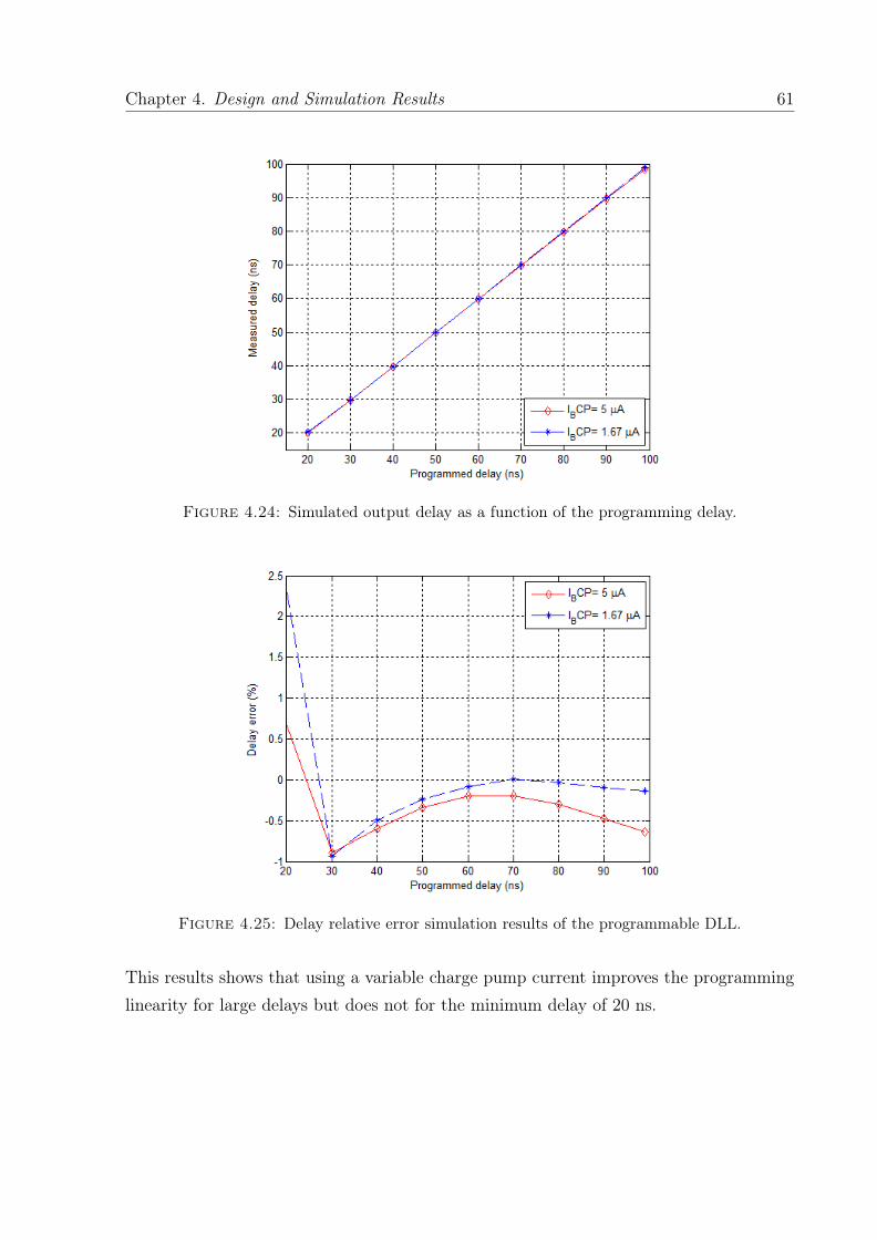
Chapter 4. Design and Simulation Results 61
Figure 4.24: Simulated output delay as a function of the programming delay.
Figure 4.25: Delay relative error simulation results of the programmable DLL.
This results shows that using a variable charge pump current improves the programminglinearity for large delays but does not for the minimum delay of 20 ns.

Chapter 4. Design and Simulation Results 62
Figure 4.26: Jitter noise simulation results of the programmable DLL.
Delay Power Jitter noise rms Delay error(ns) dissipation (mW) (ps) (%)
Constant (5 µA) 20 2.28 53.7 0.6599 2.11 1199 -0.63
Variable (1.67 µA) 20 2.05 11.6 2.2999 2.31 105.1 -0.14
Table 4.18: Programmable delay results summary.

Chapter 5
Conclusion and Future Research
This thesis presents a digitally programmable delay locked loop intended for use as timinggenerator in a RADAR ranging system. The architecture presented uses a sigma deltamodulator to generate a delay unaffected by matching and a delay lock loop (DLL) tofilter the excess jitter noise from the output clock. Designs and simulations results ofthe DLL are presented, showing that by making the current of the charge pump variableresults in a improved jitter noise and delay error.
There is some possible future work. The complete design of a UWB radar sensor is themost obvious, but it is also possible to study and design a third-order DLL since it ispossible that will result in a improve ranging resolution of the radar and a better stabilityof the system.
63

Bibliography
[1] J. H. Reed, An Introduction to Ultra Wideband Communication Systems. PrenticeHall, 2005.
[2] N. Paulino, J. Goes, and A. Steiger-Garção, Low Power CMOS Radar Sensors.Springer, 2008.
[3] www.commsdesign.com/design_corner/OEG20020301S0021.
[4] Revision of Part 15 of the Comission´s rules regarding ultra-wideband transmissionsystems. Federal Communications Commission, First Report and Order FCC 02-48,ET docket 98-153, April 2002.
[5] Z. N. C. Huseyin Arslan and M.-G. D. Benedetto, Ultra Wideband Wireless Commu-nication. Springer, 2006.
[6] M. I. Skolnik, Introduction to RADAR systems. McGraw-Hill.
[7] C. Fowler, J. Entzminger, and J. Corum, “Assessment of ultra-wideband (uwb) tech-nology,” Aerospace and Electronic Systems Magazine, IEEE, vol. 5, no. 11, pp. 45–49, nov 1990.
[8] M. Bazes, “A novel precision mos synchronous delay line,” Solid-State Circuits, IEEEJournal of, vol. 20, no. 6, pp. 1265 – 1271, dec 1985.
[9] J. Maneatis, “Low-jitter process-independent dll and pll based on self-biased tech-niques,” Solid-State Circuits, IEEE Journal of, vol. 31, no. 11, pp. 1723 –1732, nov1996.
[10] D. S. O. Semiconductor, “Mc10e195, mc100e195 5v ecl programmable delay chip.”
[11] B. Arkin, “Realizing a production ate custom processor and timing ic containing 400independent low-power and high-linearity timing verniers,” feb. 2004, pp. 348 – 349Vol.1.
64

Bibliography 65
[12] M. Mota and J. Christiansen, “A high-resolution time interpolator based on a delaylocked loop and an rc delay line,” Solid-State Circuits, IEEE Journal of, vol. 34,no. 10, pp. 1360 –1366, oct 1999.
[13] N. Paulino, M. Serrazina, J. Goes, and A. Steiger-Garcao, “Design of a digitallyprogrammable delay-locked-loop for a low-cost ultra wide band radar receiver,” vol. 1,may 2003, pp. I–133 – I–136.
[14] B. Razavi, Design of Analog CMOS Integrated Circuits. McGraw Hill, 2001.
[15] C. Piguet and V. von Kaenel, “Logic synthesis of a pll phase frequency detector,”Computers and Digital Techniques, IEE Proceedings -, vol. 144, no. 6, pp. 381 –385,nov 1997.
[16] B. Razavi, RF Microelectronics. Prentice Hall, 1997.
[17] B. Terlemez and J. Uyemura, “The design of a differential cmos charge pump for highperformance phase-locked loops,” vol. 4, may 2004, pp. IV – 561–4 Vol.4.
[18] W. Rhee, “Design of high-performance cmos charge pumps in phase-locked loops,”vol. 2, jul 1999, pp. 545 –548.
[19] M. Soyuer, J. F. Ewen, and H. L. Chuang, “A fully monolithic 1.25 ghz cmos frequencysynthesizer,” vol. 2, jun 1994, pp. 127 –128.
[20] B. Razavi, “Monolithic phase-locked loops and clock recovery circuits,” jun 1996, pp.1 –39.
[21] G. Chien and P. Gray, “A 900-mhz local oscillator using a dll-based frequency multi-plier technique for pcs applications,” Solid-State Circuits, IEEE Journal of, vol. 35,no. 12, pp. 1996 –1999, dec 2000.
[22] Y.-J. Jung, S.-W. Lee, D. Shim, W. Kim, C. Kim, and S.-I. Cho, “A dual-loop delay-locked loop using multiple voltage-controlled delay lines,” Solid-State Circuits, IEEEJournal of, vol. 36, no. 5, pp. 784 –791, may 2001.