DIGITALLY-CONTROLLED AND ELECTRICALLY-PROGRAMMABLE … Workshops/1979 CCD79/09-2 Sakaue.pdf ·...
8
DIGITALLY-CONTROLLED AND ELECTRICALLY-PROGRAMMABLE CCD TRANSVERSAL FILTER LSI f T. Sakaue, T. Iida, *F. Tanaka, *C. Satoh and *Y. Suzuki ABSTRACT This paper will describe about a 64-stage digitally-controlled and electrically-programmable CCD transversal filter LSI which is applicable for any analog signal processing. The LSI contains a 64-stage CCD trans- versal filter with quadrantally variable tap-weighting, tap-weight gener- ator composed of 64 x 8-bit D/A converters and 64 x 9-bit static RAM's, clock pulse generator, other timing pulse generator, substrate bias gen- erator, input bias circuit and output amplifier with sample-and-hold. The distinct features of the LSI are (1) compact filter structure using de- laying, adding, subtracting and multiplying function of the CCD for quad- rantally variable tap-weighting and (2) integration of the tap-wedght generator using on-chip D/A converters and static RAM's for sure and sta- ble operation of tap-weight-programming. Evaluation result indicates that the transversal filter LSI is very useful for various classes of the signal processing in video, audio and communication systems. INTRODUCTION The electrically-programmable transversal filter (EPTF) is an ex- tremely useful device in various analog signal processing field. General classes of application are; (1) various kinds of frequency filter like low pass, band pass and high pass filter, (2) matched filter in spread- spectrum communication system and (3) automatic equalizer in video, audio and telecommunication systems. In first application, the EPTF can be ac- curately trimmed into any desired frequency response, compared with con- ventional LCR-filter. In second application, it is advantageous that the EPTF realizes the matched filter by only one device, compared with con- ventional filter bank method. The filter in third application must be fully electrically programmable for external control. Charge-coupled device (CCD) offers an attractive approach to imple- mentation of the EPTF. since the CCD can directly deal the analog wave- form without analog-to-digital converter and can easily integrate any MOS peripheral circuits on the same chip, we can probably obtain the very compact, low-cost and high-reliability filters. However, the CCD-EPTF i n previous literature has generally consisted o f CCD tapped delay line, MOS multipliers and MOS summing circuits. In this case, the transfer effi- ciency tends to deteriorate due to tapped CCD's structure using floating diffusion or floating gate. The chip size also tends to become larger due to complexity of on-chip MOS circuits for multiplying and summing. Another problem in the previous literature is to be necessary for many tap-weighting leads, which causes the increase of IC pin outs. One of the solutions to reduce the pin outs is to integrate a tap-weight generator like combination of C-memories and analog switches. By this way, each tap-weight can be programmed through serial analog data, however the ana- log data are only temporally stored in the C-memories and then they must * Toshiba Corporation, Semiconductor Division. 1, Toshiba-cho, Komukai, Saiwai-ku, Kawasaki-city, Japan 222 .
Transcript of DIGITALLY-CONTROLLED AND ELECTRICALLY-PROGRAMMABLE … Workshops/1979 CCD79/09-2 Sakaue.pdf ·...
DIGITALLY-CONTROLLED AND ELECTRICALLY-PROGRAMMABLE CCD TRANSVERSAL FILTER LSI
fT. Sakaue, T. I i d a , *F. Tanaka, *C. Satoh and *Y. Suzuki
ABSTRACT
This paper w i l l describe about a 64-stage d i g i t a l l y - c o n t r o l l e d and electrically-programmable CCD t r a n s v e r s a l f i l t e r LSI which i s appl i c a b l e f o r any analog s i g n a l processing. The LSI contains a 64-stage CCD t r a n s v e r s a l f i l t e r w i t h q u a d r a n t a l l y v a r i a b l e tap-weighting, tap-weight genera t o r composed of 64 x 8 - b i t D/A converters and 64 x 9 - b i t s t a t i c RAM's, clock pulse generator, other t i m i n g pulse generator, substrate bias gene r a t o r , i n p u t bias c i r c u i t and output a m p l i f i e r w i t h sample-and-hold. The d i s t i n c t features of the LSI are (1) compact f i l t e r s t r u c t u r e using del a y i n g , adding, s u b t r a c t i n g and m u l t i p l y i n g f u n c t i o n of the CCD f o r quadr a n t a l l y v a r i a b l e tap-weighting and (2) i n t e g r a t i o n o f the tap-wedght generator using on-chip D/A converters and s t a t i c RAM's f o r sure and st a ble operation of tap-weight-programming. Evaluation r e s u l t i n d i c a t e s t h a t the t r a n s v e r s a l f i l t e r LSI i s very u s e f u l f o r various classes of the s i g n a l processing i n video, audio and communication systems.
INTRODUCTION
The electrically-programmable t r a n s v e r s a l f i l t e r (EPTF) i s an extremely u s e f u l device i n various analog s i g n a l processing f i e l d . General classes of a p p l i c a t i o n are; (1) various kinds o f frequency f i l t e r l i k e low pass, band pass and high pass f i l t e r , (2) matched f i l t e r i n spread-spectrum communication system and (3) automatic equalizer i n video, audio and telecommunication systems. I n f i r s t a p p l i c a t i o n , the EPTF can be acc u r a t e l y trimmed i n t o any desired frequency response, compared w i t h conv e n t i o n a l L C R - f i l t e r . I n second a p p l i c a t i o n , i t i s advantageous t h a t the EPTF r e a l i z e s the matched f i l t e r by only one device, compared w i t h conv e n t i o n a l f i l t e r bank method. The f i l t e r i n t h i r d a p p l i c a t i o n must be f u l l y e l e c t r i c a l l y programmable f o r e x t e r n a l c o n t r o l .
Charge-coupled device (CCD) o f f e r s an a t t r a c t i v e approach t o implementation o f the EPTF. since the CCD can d i r e c t l y deal the analog waveform w i t h o u t a n a l o g - t o - d i g i t a l converter and can e a s i l y i n t e g r a t e any MOS p e r i p h e r a l c i r c u i t s on the same chip , we can probably o b t a i n the very compact, low-cost and h i g h - r e l i a b i l i t y f i l t e r s . However, the CCD-EPTF i n previous l i t e r a t u r e has gen e r a l l y consisted o f CCD tapped delay l i n e , MOS m u l t i p l i e r s and MOS summing c i r c u i t s . I n t h i s case, the t r a n s f e r e f f i ciency tends t o d e t e r i o r a t e due t o tapped CCD's s t r u c t u r e using f l o a t i n g d i f f u s i o n o r f l o a t i n g gate. The chip size also tends t o become l a r g e r due t o complexity of on-chip MOS c i r c u i t s f o r m u l t i p l y i n g and summing. Another problem i n the previous l i t e r a t u r e i s to be necessary f o r many tap-weighting leads, which causes the increase of IC p i n outs. One of the so l u t i o n s t o reduce the p i n outs i s to i n t e g r a t e a tap-weight generator l i k e combination of C-memories and analog switches. By t h i s way, each tap-weight can be programmed through s e r i a l analog data, however the analo g data are only temporally stored i n the C-memories and then they must
* Toshiba Corporation, Semiconductor D i v i s i o n . 1, Toshiba-cho, Komukai, Saiwai-ku, Kawasaki-city, Japan
222 .
be refreshed i n an every short i n t e r v a l . To solve the above problems, a new type of CCD LSI has been developed.
CCD LSI ARCHITECTURE
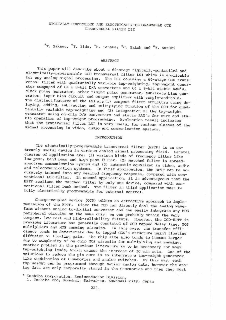
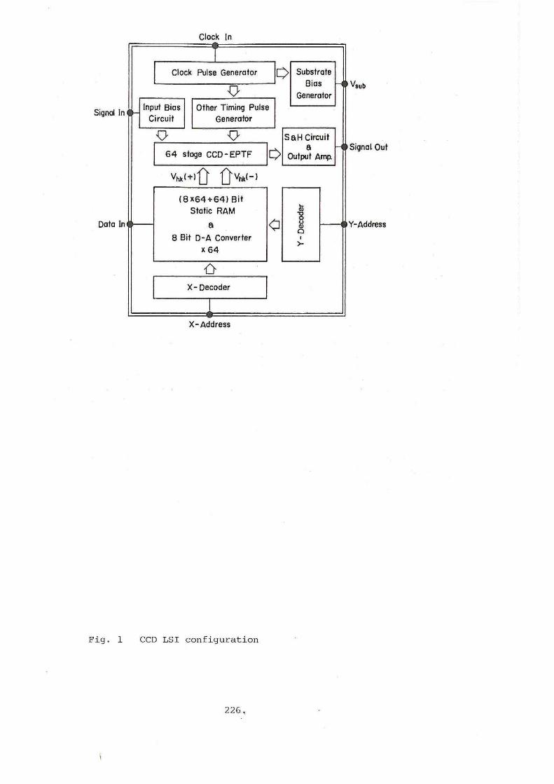
The CCD LSI contains a l l p e r i p h e r a l c i r c u i t s r e q u i r e d f o r the CCD oper a t i o n . The o v e r a l l chip dimensions are 4.30 mm by 4.60 mm and about 2/3 o f the chip area i s occupied by the tap-weight generator t o be descr i b e d l a t e r . The CCD LSI c o n f i g u r a t i o n and the photomicrograph i s shown i n F i g . 1. The f u n c t i o n of these elements are described below.
CD The 64-stage CCD-EPTF co n s i s t s o f only a 64-stage CCD delay l i n e w i t h an- i n p u t p o r t a t each stage. The EPTF a c t i o n i s achieved using d e l a y i n g , adding, s u b t r a c t i n g and m u l t i p l y i n g f u n c t i o n o f the CCD. An output s i g n a l i s sensed by means o f a f l o a t i n g d i f f u s i o n a t a f i n a l stage. D e t a i l s are described i n next s e c t i o n .
(2) The tap-weight generator co n s i s t s of 64 by 8 - b i t D/A converters, 64 by 9 - b i t s t a t i c RAM's and two address decoders. The generator o r i g i n a t e s the c o n t r o l s i g n a l s according t o s e r i a l d i g i t a l data, supplying each CCD stage. D e t a i l s are also described i n l a t e r s e c t i o n .
(3) The clock pulse generator o r i g i n a t e s two separate clock pulses from a s i n u s o i d a l clock s i g n a l i n p u t . One w i t h one-phase i s supplied the CCD of about 35pF c a p a c i t i v e load. Another w i t h two-phase i s used a t the master clock o f the other t i m i n g pulse.
(4) The other t i m i n g pulse generator has two kinds o f pulse generator. One i s f o r c h a r g e - i n j e c t i o n / r e j e c t i o n i n the CCD i n p u t p o r t s . Another i s f o r sample-and-hold o f the output s i g n a l sensed a t the f l o a t i n g d i f f u s i o n . A l l pulses w e l l operate by frequency of 15 MHz.
(5) The subs t r a t e bias generator o r i g i n a t e s a constant v o l t a g e o f about -5V by means o f the clock pulse r e c t i f i c a t i o n , supplying the s u b s t r a t e .
(6) The i n p u t bias c i r c u i t a u t o m a t i c a l l y generates optimum i n p u t DC bias l e v e l f o r wide dynamic range and high l i n e a r i t y .
(7) The output a m p l i f i e r w i t h sample-and-hold, r e c e i v i n g the s i g n a l sensed by the f l o a t i n g d i f f u s i o n , increases the s i g n a l v o l t a g e and c u r r e n t , and reduces the clock pulse component.
The LSI was f a b r i c a t e d using double p o l y - S i BCCD/NMOS process and one l e v e l p o l y - S i v/ith h igh r e s i s t i v i t y i s used f o r load r e s i s t o r s of the s t a t i c RAM c i r c u i t s ,
CCD-EPTF OPERATION
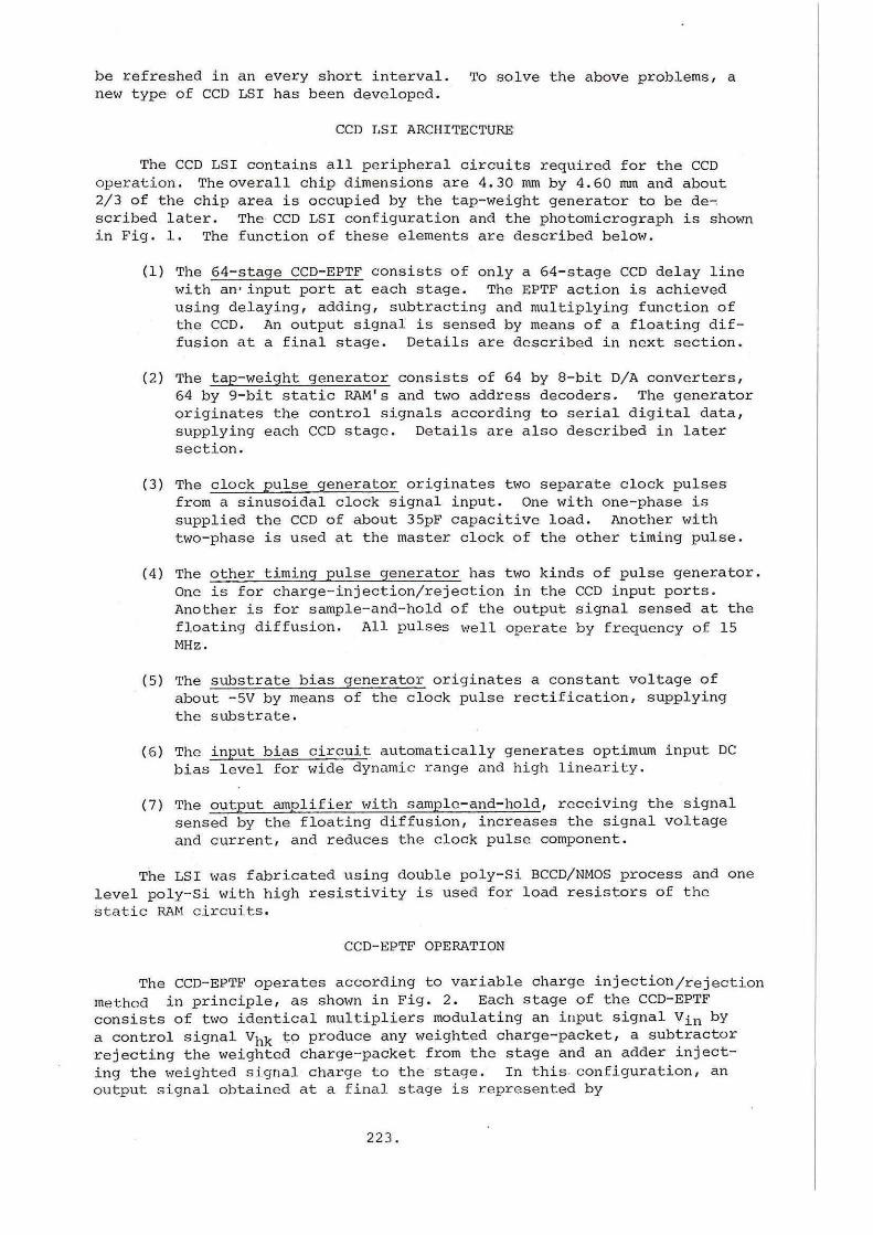
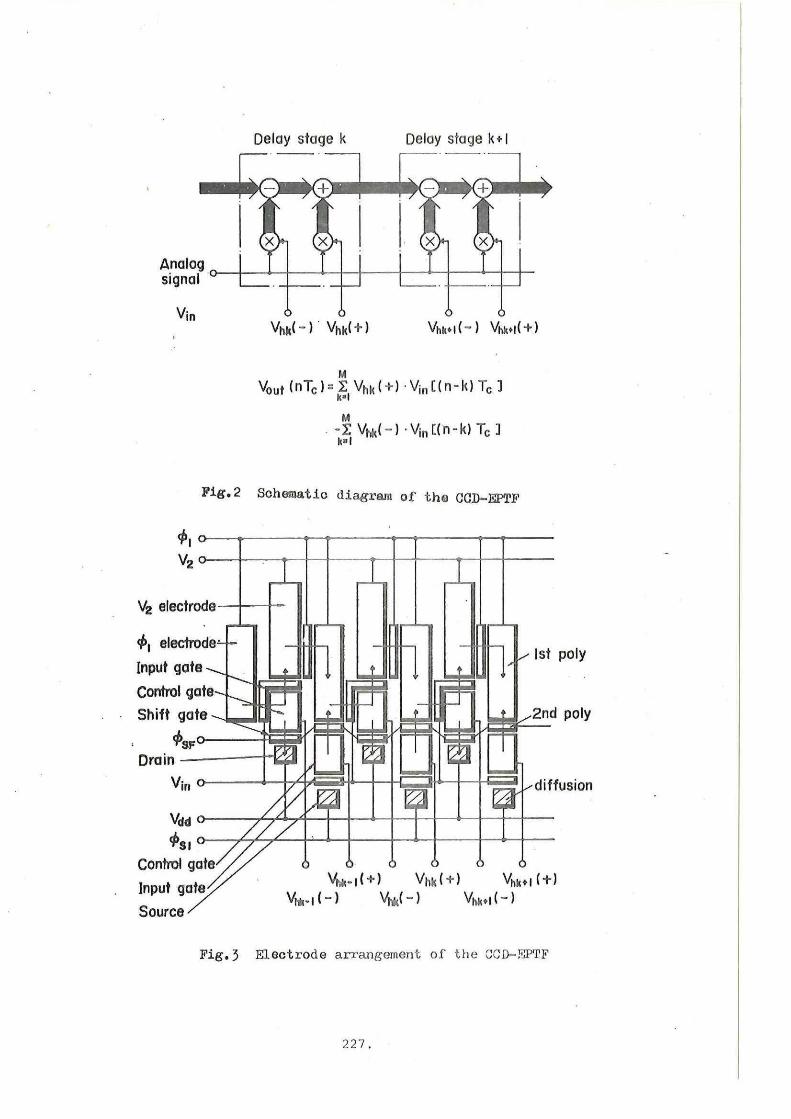
The CCD-EPTF operates according to v a r i a b l e charge i n j e c t i o n / r e j e c t i o n method i n p r i n c i p l e , as shown i n F i g . 2. Each stage o f the CCD-EPTF co n s i s t s o f two i d e n t i c a l m u l t i p l i e r s modulating an i n p u t s i g n a l Vj_ n by a c o n t r o l s i g n a l t o produce any weighted charge-packet, a s u b t r a c t o r r e j e c t i n g the weighted charge-packet from the stage and an adder i n j e c t i n g the weighted s i g n a l charge t o the"stage. I n t h i s c o n f i g u r a t i o n , an output s i g n a l obtained a t a f i n a l stage i s represented by
223.
M M W t " T c ) - E C 1 - V h k ( + ) - V i n [ ( n - k ) T c ] - S C 2 - V h k ( - ) . V i n [ ( n - k ) T c ]
k= l k = l
where V i n (kT c) i s a sampled i n p u t s i g n a l and T Q i s a u n i t delay time. This equation shows t h a t the schematic diagram i n F i g . 2 i s e x a c t l y ident i c a l w i t h a conventional t r a n s v e r s a l f i l t e r .
E lectrode arrangement of the CCD-EPTF i s shown i n F i g . 3. From f i r s t stage t o f i n a l stage, s i g n a l charge-packets are t r a n s f e r e d by a clock pulse f-£ and a constant v o l t a g e V 2 • I n any stage, f i r s t , a precedi n g (Jij e l e c t r o d e charge-packet i s t r a n s f e r e d and store d i n t o a V2 e l e c trode through an i n p u t gate a p p l i e d an i n p u t s i g n a l V^n and a c o n t r o l gate a p p l i e d a c o n t r o l s i g n a l (~) when the (f> pulse goes down. A r e mained charge-packet i n the c o n t r o l gate i s r e j e c t e d i n t o a d r a i n through a s h i f t gate when a s h i f t pulse <j>SF goes up, whose amount equals product of w e l l capacitance of the c o n t r o l gate and channel p o t e n t i a l d i f f e r e n c e between the i n p u t gate and the s h i f t gate. Since the w e l l capacitance i s approximately p r o p o r t i o n a l t o the c o n t r o l s i g n a l , the r e j e c t e d charge-packet i s also p r o p o r t i o n a l t o product o f the i n p u t s i g n a l V-j_n and the c o n t r o l s i g n a l V i ^ ( - ) . Second, the V 2 e l e c t r o d e charge-packet i s t r a n s f e r e d and stored i n t o next tyj e l e c t r o d e when the $i pulse goes up. Simultaneously, a store d charge-packet i n another c o n t r o l gate i s i n j e c t -ed i n t o the pj- e l e c t r o d e through another s h i f t gate when the s h i f t pulse <t>gp goes up, according t o the well-known F i l l and S p i l l method, whose amount i s determined by the same way as described above. Therefore, the i n j e c t e d charge-packet i s p r o p o r t i o n a l t o product of the i n p u t s i g n a l V^n and another c o n t r o l s i g n a l V n k ( + ) .
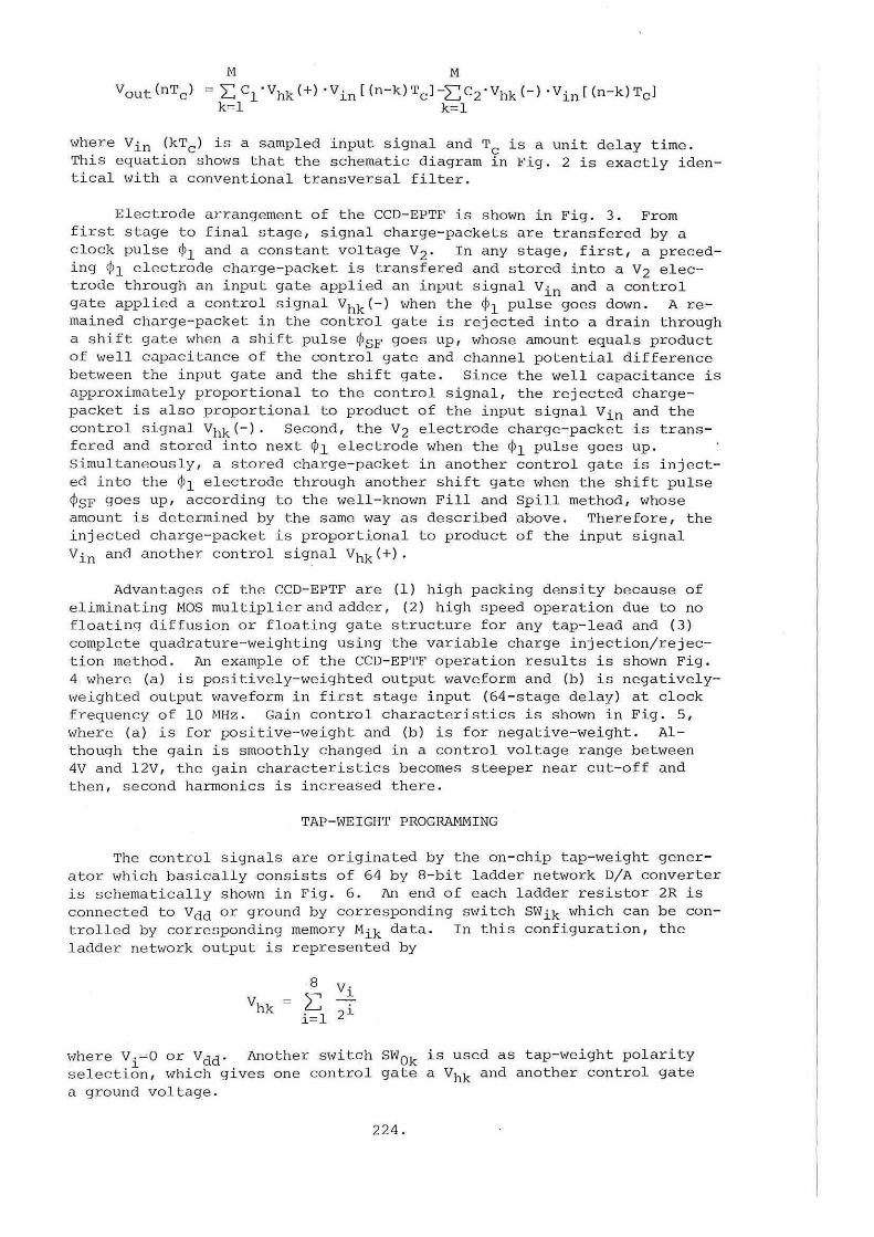
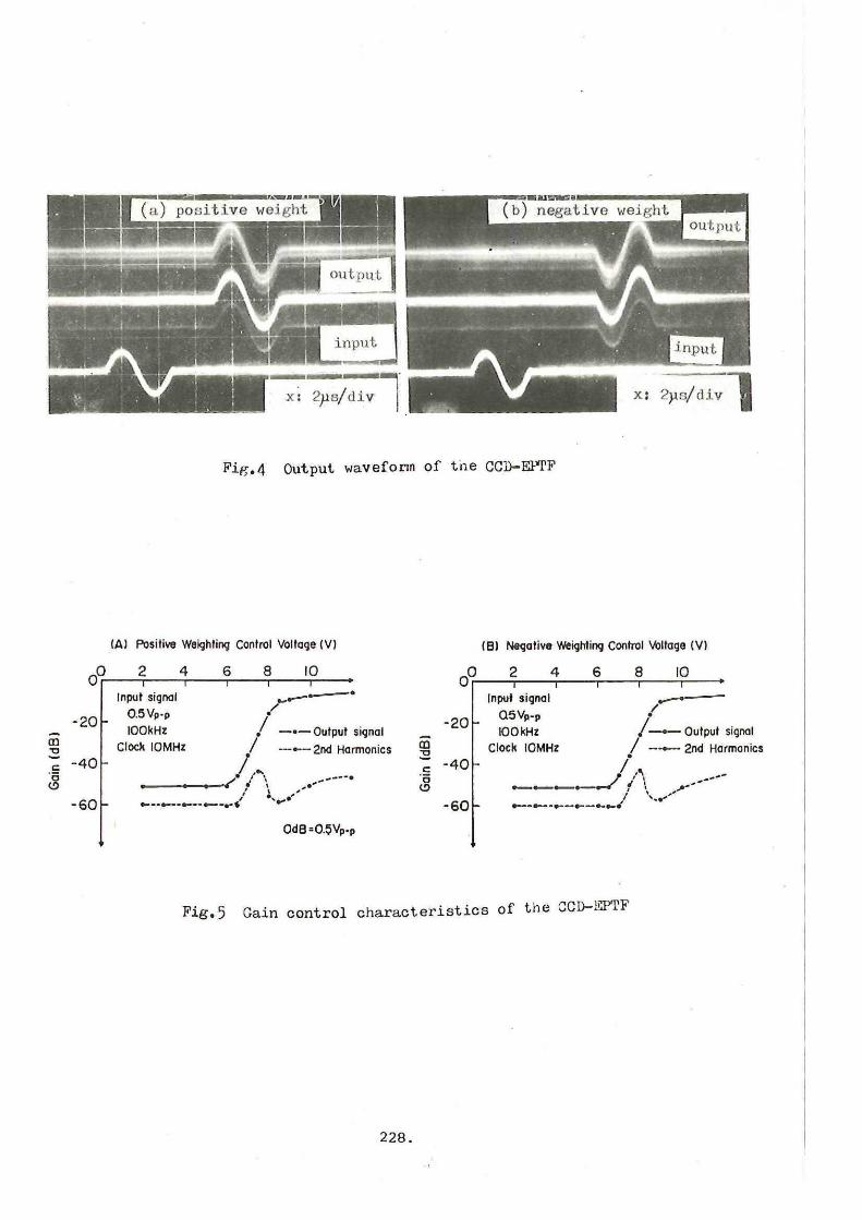
Advantages of the CCD-EPTF are (1) high packing d e n s i t y because of e l i m i n a t i n g MOS m u l t i p l i e r and adder, (2) high speed op e r a t i o n due t o no f l o a t i n g d i f f u s i o n or f l o a t i n g gate s t r u c t u r e f o r any tap-lead and (3) complete quadrature-weighting using the v a r i a b l e charge i n j e c t i o n / r e j e c t i o n method. An example of the CCD-EPTF o p e r a t i o n r e s u l t s i s shown F i g . 4 where (a) i s p o s i t i v e l y - w e i g h t e d output waveform and (b) i s n e g a t i v e l y -weighted output waveform i n f i r s t stage i n p u t (64-stage delay) a t clock frequency o f 10 MHz. Gain c o n t r o l c h a r a c t e r i s t i c s i s shown i n F i g . 5, v/here (a) i s f o r p o s i t i v e - w e i g h t and (b) i s f o r negative-weight. A l though the gain i s smoothly changed i n a c o n t r o l v o l t a g e range between 4V and 12V, the gain c h a r a c t e r i s t i c s becomes steeper near c u t - o f f and then, second harmonics i s increased t h e r e .
TAP-WEIGHT PROGRAMMING
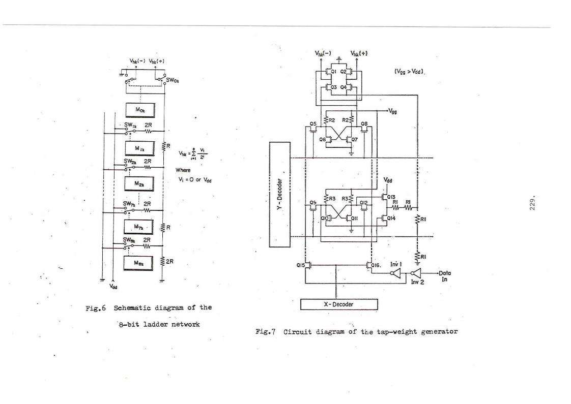
The c o n t r o l s i g n a l s are o r i g i n a t e d by the on-chip tap-weight genera t o r which b a s i c a l l y c o n s i s t s of 64 by 8 - b i t ladder network D/A converter i s s c h e m a t i c a l l y shown i n F i g . 6. An end o f each ladder r e s i s t o r 2R i s connected t o V33 or ground by corresponding switch SW-jj v/hich can be cont r o l l e d by corresponding memory M^k data. I n t h i s c o n f i g u r a t i o n , the ladder network output i s represented by
V hk
0 V-j
where V-=0 or V d d- Another s w i t c h SWQk i s used as tap-weight p o l a r i t y s e l e c t i o n , which gives one c o n t r o l gate a V n J c and another c o n t r o l gate a ground v o l t a g e .
224.
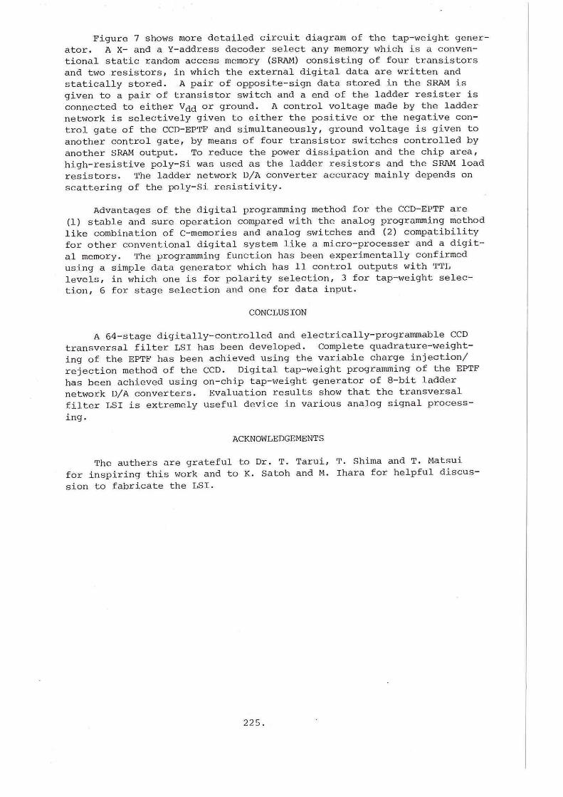
F i g u r e 7 shows more d e t a i l e d c i r c u i t diagram of the tap-weight gener
a t o r . A X- and a Y-address decoder s e l e c t any memory which i s a conven
t i o n a l s t a t i c random a c c e s s memory (SRAM) c o n s i s t i n g of four t r a n s i s t o r s
and two r e s i s t o r s , i n which the e x t e r n a l d i g i t a l d a t a a r e w r i t t e n and
s t a t i c a l l y s t o r e d . A p a i r of o p p o s i t e - s i g n data s t o r e d i n the SRAM i s
given to a p a i r of t r a n s i s t o r s w i t c h and a end of the la d d e r r e s i s t e r i s
connected to e i t h e r or ground. A c o n t r o l v o l t a g e made by the ladder
network, i s s e l e c t i v e l y g i v e n to e i t h e r the p o s i t i v e or the n e g a t i v e con
t r o l gate of the CCD-EPTF and s i m u l t a n e o u s l y , ground v o l t a g e i s g i v e n to
another c o n t r o l gate, by means of four t r a n s i s t o r s w i t c h e s c o n t r o l l e d by
another SRAM output. To reduce the power d i s s i p a t i o n and the c h i p a r e a ,
h i g h - r e s i s t i v e p o l y - S i was used as the ladder r e s i s t o r s and the SRAM l o a d
r e s i s t o r s . The ladder network D/A c o n v e r t e r a c c u r a c y mainly depends on
s c a t t e r i n g of the p o l y - S i r e s i s t i v i t y .
Advantages of the d i g i t a l programming method f o r the CCD-EPTF a r e
(1) s t a b l e and sure o p e r a t i o n compared w i t h the analog programming method
l i k e combination of C-memories and analog s w i t c h e s and (2) c o m p a t i b i l i t y
f o r o t h e r c o n v e n t i o n a l d i g i t a l system l i k e a m i c r o - p r o c e s s e r and a d i g i t
a l memory. The programming f u n c t i o n has been e x p e r i m e n t a l l y confirmed
u s i n g a simple data generator which has 11 c o n t r o l outputs w i t h TTL
l e v e l s , i n which one i s f o r p o l a r i t y s e l e c t i o n , 3 f o r tap-weight s e l e c
t i o n , 6 f o r stage s e l e c t i o n and one f o r data input.
CONCLUSION
A 64-stage d i g i t a l l y - c o n t r o l l e d and e l e c t r i c a l l y - p r o g r a m m a b l e CCD
t r a n s v e r s a l f i l t e r L S I has been developed. Complete quadrature-weight
ing of the EPTF has been achieved u s i n g the v a r i a b l e charge i n j e c t i o n /
r e j e c t i o n method of the CCD. D i g i t a l tap-weight programming of the EPTF
has been achieved u s i n g on-chip tap-weight generator of 8 - b i t l a d d e r
network D/A c o n v e r t e r s . E v a l u a t i o n r e s u l t s show t h a t the t r a n s v e r s a l
f i l t e r L S I i s extremely u s e f u l d e v i c e i n v a r i o u s analog s i g n a l p r o c e s s
ing.
ACKNOWLEDGEMENTS
The a u t h e r s are g r a t e f u l to Dr. T. T a r u i , T. Shima and T. Matsui
f o r i n s p i r i n g t h i s work and to K. Satoh and M. I h a r a f o r h e l p f u l d i s c u s
s i o n to f a b r i c a t e the L S I .
225.
Clock In
Clock Pulse Generator
Input Bias
Circuit
Other Timing Pulse Generator
6 4 stage C C D - E P T F
( 8 x 6 4 + 6 4 ) Bit
Static RAM
a
8 Bit D-A Converter
x 64
X - Decoder
Substrate
Bias
Generator V8Ub
S a H Circuit a
Output Amp.
o O u 0) a
Signal Out
>Y-Address
X-Address
F i g . 1 CCD L S I c o n f i g u r a t i o n
226,
Analog signal
Delay stage k Delay stage k +
Vhh(-)' Vh°h( + » V h k H ( - ) vwi<+:
Vout(nT c) = 2 V h k ( + ) - V i n C ( n - k ) T c ]
- S V ^ - J - V i n K n - W T c ]
Piff.2 Sohematio diagram o f the GGD-EPTF
V 2 electrode
4>i electrode^-r-
Input gate
Control gate
Shift gate
Drain
Control gate
Input gate
Source
1st poly
1 f I ^?nd poly
diffusion
ó ö ö o Ö
Fig. 3 Electrode a r rangemen t of t h e GGD-EPTF
227 .
(A) Positive Weighting Control Voltage (V) (B) Negativo Weighting Control Voltage (V)
CD •a
0
-20
-40
-60
.0 8 10
Input signal
0.5Vp-p
100kHz
Clock 10MHz
/ J — • — O u t p u t signal
/ — • — 2 n d Harmonics
—•—•—
OdB=0.5Vp-p
CD
£ ' 5 to
-20r-
-40
-60
l r
Input signal
Q 5 V p - p
100kHz
Clock 10MHz
10
. — — — . —
/_ - Output signal
2nd Harmonics
Fig . 5 Gain control charac te r i s t ics of the CCD-13PTF
2 2 8 .
V h k ( - ) V h k ( + )
Mot
SW I k 2R •«3 Q I . .
:
b HST sw0k
• Vi
Where
Vj = O or V d d
SW 8 k 2R
3^—vw—\
M 2R
Fig,6 Schematic diagram of the
' 8 - b i t ladder network
VhkM Vhk(+)
3L (Vgg >Vdd).
<h<3— I Inv2 I n
CM
X - Decoder
Fig.7 C i r cu i t diagram of the tap-weight generator