Digital Temperature Sensor with Two-Wire Interface and ... · • Electrical Motor Driver Thermal...
31
±3 ±2 ±1 0 1 2 3 ±75 ±50 ±25 0 25 50 75 100 125 150 Temperature Error (C) Temperature (C) Mean Mean - 6 Mean + 6 C005 A2 SDA SCL GND ALERT 2 6 8 7 1 A1 A0 VS 4 3 5 0.01 2F Two-Wire Host Controller TMP75B 1.4 V to 3.6 V Product Folder Sample & Buy Technical Documents Tools & Software Support & Community TMP75B SBOS706B – APRIL 2014 – REVISED AUGUST 2014 TMP75B 1.8-V Digital Temperature Sensor with Two-Wire Interface and Alert 1 Features 3 Description The TMP75B is an integrated digital temperature 1• Low-Voltage Alternative to LM75 and TMP75 sensor with a 12-bit analog-to-digital converter (ADC) • Digital Output with Standard Two-Wire Serial that can operate at a 1.8-V supply, and is pin and Interface register compatible with the industry-standard LM75 • Up to 8 Pin-Programmable Bus Addresses and TMP75. This device is available in SOIC-8 and VSSOP-8 packages, and requires no external • Overtemperature ALERT Pin with Programmable components to sense the temperature. The TMP75B Trip Values is capable of reading temperatures with a resolution • Shutdown Mode for Battery Power Saving of 0.0625°C and is specified over a temperature • One-Shot Conversion Mode for Custom Update range of –55°C to +125°C. Rates The TMP75B features SMBus and two-wire interface • Operating Temperature Range: –55°C to +125°C compatibility, and allows up to eight devices on the same bus with the SMBus overtemperature alert • Operating Supply Range: 1.4 V to 3.6 V function. The programmable temperature limits and • Quiescent Current: the ALERT pin allow the sensor to operate as a – 45 μA Active (typ) stand-alone thermostat, or an overtemperature alarm – 0.3 μA Shutdown (typ) for power throttling or system shutdown. • Accuracy: The factory-calibrated temperature accuracy and the noise-immune digital interface make the TMP75B the – ±0.5°C (typ) from –20°C to +85°C preferred solution for temperature compensation of – ±1°C (typ) from –55°C to +125°C other sensors and electronic components, without the • Resolution: 12 Bits (0.0625°C) need for additional system-level calibration or • Packages: SOIC-8 and VSSOP-8 elaborate board layout for distributed temperature sensing. 2 Applications The TMP75B is ideal for thermal management and protection of a variety of consumer, computer, • Server and Computer Thermal Management communication, industrial, and environmental • Telecommunication Equipment applications. • Office Machines • Video Game Consoles Device Information (1) • Set-Top Boxes DEVICE NAME PACKAGE BODY SIZE (NOM) SOIC (8) 4.90 mm × 3.90 mm • Power Supply and Battery Thermal Protection TMP75B VSSOP (8) 3.00 mm × 3.00 mm • Thermostat Control (1) For all available packages, see the package option addendum • Environmental Monitoring and HVAC at the end of the datasheet. • Electrical Motor Driver Thermal Protection Temperature Accuracy (Error) vs Ambient Simplified Schematic Temperature 1 An IMPORTANT NOTICE at the end of this data sheet addresses availability, warranty, changes, use in safety-critical applications, intellectual property matters and other important disclaimers. PRODUCTION DATA.
Transcript of Digital Temperature Sensor with Two-Wire Interface and ... · • Electrical Motor Driver Thermal...
±3
±2
±1
0
1
2
3
±75 ±50 ±25 0 25 50 75 100 125 150
Tem
pera
ture
Err
or (�C
)
Temperature (�C)
Mean
Mean - 61
Mean + 61
C005
A2
SDA
SCL
GND
ALERT
2
6
8
7
1
A1
A0
VS
4
3
5
0.01 PF
Two-WireHost Controller
TMP75B
1.4 V to 3.6 V
Product
Folder
Sample &Buy
Technical
Documents
Tools &
Software
Support &Community
TMP75BSBOS706B –APRIL 2014–REVISED AUGUST 2014
TMP75B 1.8-V Digital Temperature Sensor with Two-Wire Interface and Alert1 Features 3 Description
The TMP75B is an integrated digital temperature1• Low-Voltage Alternative to LM75 and TMP75
sensor with a 12-bit analog-to-digital converter (ADC)• Digital Output with Standard Two-Wire Serial that can operate at a 1.8-V supply, and is pin andInterface register compatible with the industry-standard LM75
• Up to 8 Pin-Programmable Bus Addresses and TMP75. This device is available in SOIC-8 andVSSOP-8 packages, and requires no external• Overtemperature ALERT Pin with Programmablecomponents to sense the temperature. The TMP75BTrip Valuesis capable of reading temperatures with a resolution
• Shutdown Mode for Battery Power Saving of 0.0625°C and is specified over a temperature• One-Shot Conversion Mode for Custom Update range of –55°C to +125°C.
Rates The TMP75B features SMBus and two-wire interface• Operating Temperature Range: –55°C to +125°C compatibility, and allows up to eight devices on the
same bus with the SMBus overtemperature alert• Operating Supply Range: 1.4 V to 3.6 Vfunction. The programmable temperature limits and• Quiescent Current:the ALERT pin allow the sensor to operate as a
– 45 μA Active (typ) stand-alone thermostat, or an overtemperature alarm– 0.3 μA Shutdown (typ) for power throttling or system shutdown.
• Accuracy: The factory-calibrated temperature accuracy and thenoise-immune digital interface make the TMP75B the– ±0.5°C (typ) from –20°C to +85°Cpreferred solution for temperature compensation of– ±1°C (typ) from –55°C to +125°Cother sensors and electronic components, without the
• Resolution: 12 Bits (0.0625°C) need for additional system-level calibration or• Packages: SOIC-8 and VSSOP-8 elaborate board layout for distributed temperature
sensing.2 Applications The TMP75B is ideal for thermal management and
protection of a variety of consumer, computer,• Server and Computer Thermal Managementcommunication, industrial, and environmental• Telecommunication Equipmentapplications.• Office Machines
• Video Game Consoles Device Information(1)
• Set-Top Boxes DEVICE NAME PACKAGE BODY SIZE (NOM)SOIC (8) 4.90 mm × 3.90 mm• Power Supply and Battery Thermal Protection
TMP75BVSSOP (8) 3.00 mm × 3.00 mm• Thermostat Control
(1) For all available packages, see the package option addendum• Environmental Monitoring and HVACat the end of the datasheet.• Electrical Motor Driver Thermal Protection
Temperature Accuracy (Error) vs AmbientSimplified Schematic Temperature
1
An IMPORTANT NOTICE at the end of this data sheet addresses availability, warranty, changes, use in safety-critical applications,intellectual property matters and other important disclaimers. PRODUCTION DATA.
TMP75BSBOS706B –APRIL 2014–REVISED AUGUST 2014 www.ti.com
Table of Contents7.4 Device Functional Modes........................................ 151 Features .................................................................. 17.5 Programming........................................................... 162 Applications ........................................................... 17.6 Register Map........................................................... 163 Description ............................................................. 1
8 Application and Implementation ........................ 194 Revision History..................................................... 28.1 Application Information............................................ 195 Pin Configuration and Functions ......................... 38.2 Typical Application ................................................. 196 Specifications......................................................... 4
9 Power Supply Recommendations ...................... 206.1 Absolute Maximum Ratings ...................................... 410 Layout................................................................... 216.2 Handling Ratings....................................................... 4
10.1 Layout Guidelines ................................................. 216.3 Recommended Operating Conditions....................... 410.2 Layout Example .................................................... 216.4 Thermal Information .................................................. 4
11 Device and Documentation Support ................. 226.5 Electrical Characteristics........................................... 511.1 Documentation Support ....................................... 226.6 Typical Characteristics .............................................. 611.2 Trademarks ........................................................... 227 Detailed Description .............................................. 711.3 Electrostatic Discharge Caution............................ 227.1 Overview ................................................................... 711.4 Glossary ................................................................ 227.2 Functional Block Diagram ......................................... 7
12 Mechanical, Packaging, and Orderable7.3 Feature Description................................................... 8Information ........................................................... 22
4 Revision History
Changes from Revision A (April 2014) to Revision B Page
• Added DGK (VSSOP-8) package to data sheet .................................................................................................................... 1
Changes from Original (April 2014) to Revision A Page
• Changed from product preview to production data ................................................................................................................ 1
2 Submit Documentation Feedback Copyright © 2014, Texas Instruments Incorporated
Product Folder Links: TMP75B
A2
SDA
SCL
GND
ALERT
2
6
8
7
1
A1
A0
VS
4
3
5
TMP75Bwww.ti.com SBOS706B –APRIL 2014–REVISED AUGUST 2014
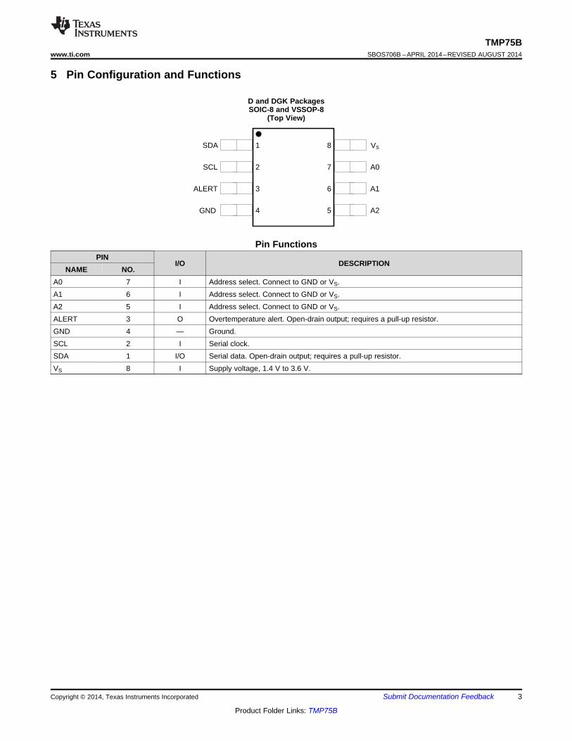
5 Pin Configuration and Functions
D and DGK PackagesSOIC-8 and VSSOP-8
(Top View)
Pin FunctionsPIN
I/O DESCRIPTIONNAME NO.
A0 7 I Address select. Connect to GND or VS.A1 6 I Address select. Connect to GND or VS.A2 5 I Address select. Connect to GND or VS.ALERT 3 O Overtemperature alert. Open-drain output; requires a pull-up resistor.GND 4 — Ground.SCL 2 I Serial clock.SDA 1 I/O Serial data. Open-drain output; requires a pull-up resistor.VS 8 I Supply voltage, 1.4 V to 3.6 V.
Copyright © 2014, Texas Instruments Incorporated Submit Documentation Feedback 3
Product Folder Links: TMP75B

TMP75BSBOS706B –APRIL 2014–REVISED AUGUST 2014 www.ti.com
6 Specifications
6.1 Absolute Maximum Ratingsover operating free-air temperature range (unless otherwise noted) (1)
MIN MAX UNITSupply voltage, VS 4 V
SDA, SCL, ALERT, A2, A1 -0.3 4 VInput voltage
A0 -0.3 (VS) + 0.3 VSink current SDA, ALERT 10 mAOperating junction temperature -55 150 °C
(1) Stresses beyond those listed under Absolute Maximum Ratings may cause permanent damage to the device. These are stress ratingsonly, which do not imply functional operation of the device at these or any other conditions beyond those indicated under RecommendedOperating Conditions. Exposure to absolute-maximum-rated conditions for extended periods may affect device reliability.
6.2 Handling RatingsMIN MAX UNIT
Tstg Storage temperature range -60 150 °CHuman body model (HBM), per ANSI/ESDA/JEDEC JS-001, all pins (1) –2000 2000ElectrostaticV(ESD) Vdischarge Charged device model (CDM), per JEDEC specification JESD22-C101, all pins (2) –1000 1000
(1) JEDEC document JEP155 states that 500-V HBM allows safe manufacturing with a standard ESD control process.(2) JEDEC document JEP157 states that 250-V CDM allows safe manufacturing with a standard ESD control process.
6.3 Recommended Operating Conditionsover operating free-air temperature range (unless otherwise noted)
MIN NOM MAX UNITSupply voltage 1.4 1.8 3.6 VOperating free-air temperature, TA -55 125 °C
6.4 Thermal InformationTMP75B
THERMAL METRIC (1) D (SOIC) DGK (VSSOP) UNIT8 PINS 8 PINS
RθJA Junction-to-ambient thermal resistance 125.4 188.1RθJC(top) Junction-to-case (top) thermal resistance 71.5 79.1RθJB Junction-to-board thermal resistance 65.8 109.6
°C/WψJT Junction-to-top characterization parameter 21.1 15.3ψJB Junction-to-board characterization parameter 65.3 108RθJC(bot) Junction-to-case (bottom) thermal resistance N/A N/A
(1) For more information about traditional and new thermal metrics, see the IC Package Thermal Metrics application report, SPRA953.
4 Submit Documentation Feedback Copyright © 2014, Texas Instruments Incorporated
Product Folder Links: TMP75B
TMP75Bwww.ti.com SBOS706B –APRIL 2014–REVISED AUGUST 2014
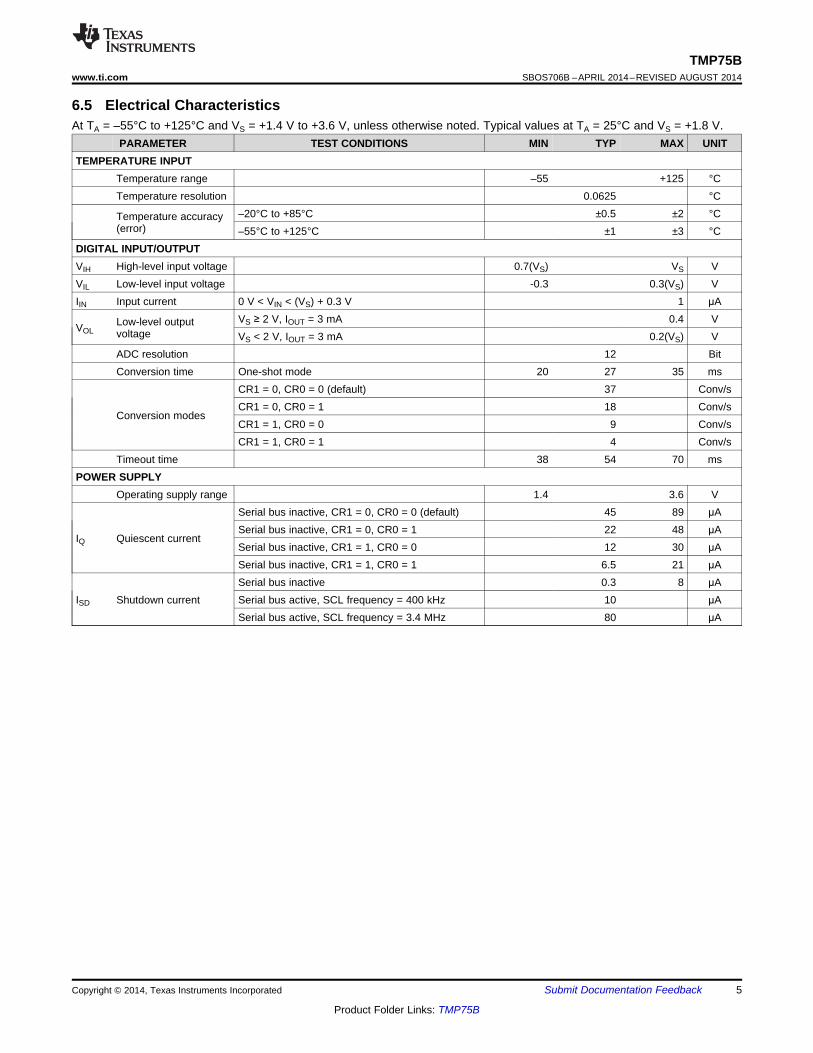
6.5 Electrical CharacteristicsAt TA = –55°C to +125°C and VS = +1.4 V to +3.6 V, unless otherwise noted. Typical values at TA = 25°C and VS = +1.8 V.
PARAMETER TEST CONDITIONS MIN TYP MAX UNITTEMPERATURE INPUT
Temperature range –55 +125 °CTemperature resolution 0.0625 °C
–20°C to +85°C ±0.5 ±2 °CTemperature accuracy(error) –55°C to +125°C ±1 ±3 °C
DIGITAL INPUT/OUTPUTVIH High-level input voltage 0.7(VS) VS VVIL Low-level input voltage -0.3 0.3(VS) VIIN Input current 0 V < VIN < (VS) + 0.3 V 1 μA
VS ≥ 2 V, IOUT = 3 mA 0.4 VLow-level outputVOL voltage VS < 2 V, IOUT = 3 mA 0.2(VS) VADC resolution 12 BitConversion time One-shot mode 20 27 35 ms
CR1 = 0, CR0 = 0 (default) 37 Conv/sCR1 = 0, CR0 = 1 18 Conv/s
Conversion modesCR1 = 1, CR0 = 0 9 Conv/sCR1 = 1, CR0 = 1 4 Conv/s
Timeout time 38 54 70 msPOWER SUPPLY
Operating supply range 1.4 3.6 VSerial bus inactive, CR1 = 0, CR0 = 0 (default) 45 89 μASerial bus inactive, CR1 = 0, CR0 = 1 22 48 μA
IQ Quiescent currentSerial bus inactive, CR1 = 1, CR0 = 0 12 30 μASerial bus inactive, CR1 = 1, CR0 = 1 6.5 21 μASerial bus inactive 0.3 8 μA
ISD Shutdown current Serial bus active, SCL frequency = 400 kHz 10 μASerial bus active, SCL frequency = 3.4 MHz 80 μA
Copyright © 2014, Texas Instruments Incorporated Submit Documentation Feedback 5
Product Folder Links: TMP75B
-1
-0.9
-0
.8
-0.7
-0
.6
-0.5
-0
.4
-0.3
-0
.2
-0.1
0 0.
1 0.
2 0.
3 0.
4 0.
5 0.
6 0.
7 0.
8 0.
9 1
Pop
ulat
ion
Temperature Error (�C) C006
±3
±2
±1
0
1
2
3
±75 ±50 ±25 0 25 50 75 100 125 150
Tem
pera
ture
Err
or (�C
)
Temperature (�C)
Mean
Mean - 61
Mean + 61
C005
20
21
22
23
24
25
26
27
28
29
30
±75 ±50 ±25 0 25 50 75 100 125 150
Con
vers
ion
Tim
e (m
s)
Temperature (�C)
Vs = 1.4V
Vs = 1.8V
Vs = 3.6V
C003
0
25
50
75
100
125
150
175
200
10 100 1000 10000
I Q (�
A)
Bus Frequency (kHz)
Ta = -��Û&
7D� ���Û&
7D� ����Û&
C004
0
10
20
30
40
50
60
70
80
90
100
±75 ±50 ±25 0 25 50 75 100 125 150
I Q (�
A)
Temperature (�C)
CR = '0h' CR = '1h' CR = '2h' CR = '3h'
C001
0
1
2
3
4
5
6
7
8
9
10
±75 ±50 ±25 0 25 50 75 100 125 150
I SD (�
A)
Temperature (�C)
Vs = 1.4V
Vs = 1.8V
Vs = 3.6V
C002
TMP75BSBOS706B –APRIL 2014–REVISED AUGUST 2014 www.ti.com
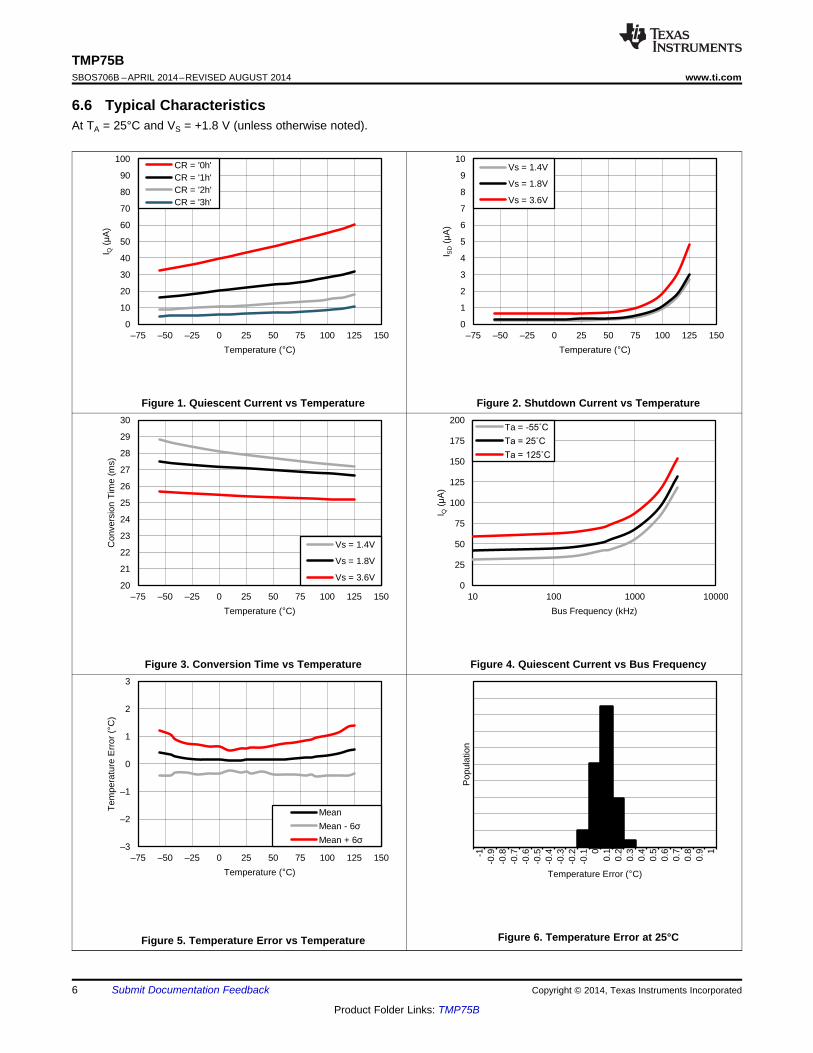
6.6 Typical CharacteristicsAt TA = 25°C and VS = +1.8 V (unless otherwise noted).
Figure 1. Quiescent Current vs Temperature Figure 2. Shutdown Current vs Temperature
Figure 3. Conversion Time vs Temperature Figure 4. Quiescent Current vs Bus Frequency
Figure 6. Temperature Error at 25°CFigure 5. Temperature Error vs Temperature
6 Submit Documentation Feedback Copyright © 2014, Texas Instruments Incorporated
Product Folder Links: TMP75B
SDA
SCL
A0
A1
A2
VS
GND
ALERTI N x I
Thermal BJT
ADC
Control Logic
Device
Register Bank
Serial Interface
OscillatorVoltage Regulator
TMP75Bwww.ti.com SBOS706B –APRIL 2014–REVISED AUGUST 2014
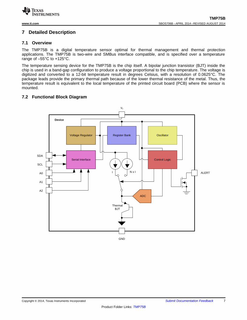
7 Detailed Description
7.1 OverviewThe TMP75B is a digital temperature sensor optimal for thermal management and thermal protectionapplications. The TMP75B is two-wire and SMBus interface compatible, and is specified over a temperaturerange of –55°C to +125°C.
The temperature sensing device for the TMP75B is the chip itself. A bipolar junction transistor (BJT) inside thechip is used in a band-gap configuration to produce a voltage proportional to the chip temperature. The voltage isdigitized and converted to a 12-bit temperature result in degrees Celsius, with a resolution of 0.0625°C. Thepackage leads provide the primary thermal path because of the lower thermal resistance of the metal. Thus, thetemperature result is equivalent to the local temperature of the printed circuit board (PCB) where the sensor ismounted.
7.2 Functional Block Diagram
Copyright © 2014, Texas Instruments Incorporated Submit Documentation Feedback 7
Product Folder Links: TMP75B

TMP75BSBOS706B –APRIL 2014–REVISED AUGUST 2014 www.ti.com
7.3 Feature Description
7.3.1 Digital Temperature OutputThe 12-bit digital output from each temperature measurement conversion is stored in the read-only temperatureregister. Two bytes must be read to obtain the data, as shown in Figure 15. Note that byte 1 is the mostsignificant byte, followed by byte 2, the least significant byte. The temperature result is left-justified with the 12most significant bits used to indicate the temperature. There is no need to read the second byte if resolutionbelow 1°C is not required. Table 1 summarizes the temperature data format. One LSB equals 0.0625°C.Negative numbers are represented in binary twos complement format.
Table 1. Temperature Data Format (1)
DIGITAL OUTPUTTEMPERATURE (°C) BINARY HEX
128 0111 1111 1111 7FF127.9375 0111 1111 1111 7FF
100 0110 0100 0000 64080 0101 0000 0000 50075 0100 1011 0000 4B050 0011 0010 0000 32025 0001 1001 0000 190
0.25 0000 0000 0100 0040 0000 0000 0000 000
–0.25 1111 1111 1100 FFC–25 1110 0111 0000 E70–55 1100 1001 0000 C90
(1) The temperature sensor resolution is 0.0625°C/LSB.
Table 1 does not supply a full list of all temperatures. Use the following rules to obtain the digital data format fora given temperature, and vice versa.
To convert positive temperatures to a digital data format:Divide the temperature by the resolution. Then, convert the result to binary code with a 12-bit, left-justifiedformat, and MSB = 0 to denote a positive sign.Example: (+50°C) / (0.0625°C / LSB) = 800 = 320h = 0011 0010 0000
To convert a positive digital data format to temperature:Convert the 12-bit, left-justified binary temperature result, with the MSB = 0 to denote a positive sign, to adecimal number. Then, multiply the decimal number by the resolution to obtain the positive temperature.Example: 0011 0010 0000 = 320h = 800 × (0.0625°C / LSB) = +50°C
To convert negative temperatures to a digital data format:Divide the absolute value of the temperature by the resolution, and convert the result to binary code with a12-bit, left-justified format. Then, generate the twos complement of the result by complementing the binarynumber and adding one. Denote a negative number with MSB = 1.Example: (|–25°C|) / (0.0625°C / LSB) = 400 = 190h = 0001 1001 0000Two's complement format: 1110 0110 1111 + 1 = 1110 0111 0000
To convert a negative digital data format to temperature:Generate the twos compliment of the 12-bit, left-justified binary number of the temperature result (with MSB= 1, denoting negative temperature result) by complementing the binary number and adding one. Thisrepresents the binary number of the absolute value of the temperature. Convert to decimal number andmultiply by the resolution to get the absolute temperature, then multiply by –1 for the negative sign.Example: 1110 0111 0000 has twos compliment of 0001 1001 0000 = 0001 1000 1111 + 1Convert to temperature: 0001 1001 0000 = 190h = 400; 400 × (0.0625°C / LSB) = 25°C = (|–25°C|);(|–25°C|) × (–1) = –25°C
8 Submit Documentation Feedback Copyright © 2014, Texas Instruments Incorporated
Product Folder Links: TMP75B
Measured
Temperature
THIGH
TLOW
Device ALERT PIN
(Comparator Mode)
POL = 0
Device ALERT PIN
(Interrupt Mode)
POL = 0
Device ALERT PIN
(Comparator Mode)
POL = 1
Device ALERT PIN
(Interrupt Mode)
POL = 1
Read Read
Time
Read
TMP75Bwww.ti.com SBOS706B –APRIL 2014–REVISED AUGUST 2014
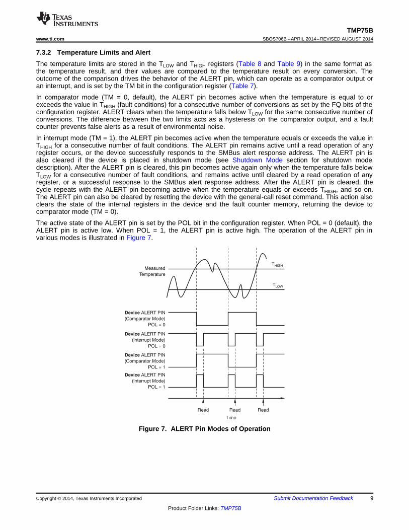
7.3.2 Temperature Limits and AlertThe temperature limits are stored in the TLOW and THIGH registers (Table 8 and Table 9) in the same format asthe temperature result, and their values are compared to the temperature result on every conversion. Theoutcome of the comparison drives the behavior of the ALERT pin, which can operate as a comparator output oran interrupt, and is set by the TM bit in the configuration register (Table 7).
In comparator mode (TM = 0, default), the ALERT pin becomes active when the temperature is equal to orexceeds the value in THIGH (fault conditions) for a consecutive number of conversions as set by the FQ bits of theconfiguration register. ALERT clears when the temperature falls below TLOW for the same consecutive number ofconversions. The difference between the two limits acts as a hysteresis on the comparator output, and a faultcounter prevents false alerts as a result of environmental noise.
In interrupt mode (TM = 1), the ALERT pin becomes active when the temperature equals or exceeds the value inTHIGH for a consecutive number of fault conditions. The ALERT pin remains active until a read operation of anyregister occurs, or the device successfully responds to the SMBus alert response address. The ALERT pin isalso cleared if the device is placed in shutdown mode (see Shutdown Mode section for shutdown modedescription). After the ALERT pin is cleared, this pin becomes active again only when the temperature falls belowTLOW for a consecutive number of fault conditions, and remains active until cleared by a read operation of anyregister, or a successful response to the SMBus alert response address. After the ALERT pin is cleared, thecycle repeats with the ALERT pin becoming active when the temperature equals or exceeds THIGH, and so on.The ALERT pin can also be cleared by resetting the device with the general-call reset command. This action alsoclears the state of the internal registers in the device and the fault counter memory, returning the device tocomparator mode (TM = 0).
The active state of the ALERT pin is set by the POL bit in the configuration register. When POL = 0 (default), theALERT pin is active low. When POL = 1, the ALERT pin is active high. The operation of the ALERT pin invarious modes is illustrated in Figure 7.
Figure 7. ALERT Pin Modes of Operation
Copyright © 2014, Texas Instruments Incorporated Submit Documentation Feedback 9
Product Folder Links: TMP75B

TMP75BSBOS706B –APRIL 2014–REVISED AUGUST 2014 www.ti.com
7.3.3 Serial InterfaceThe TMP75B operates as a slave device only on the two-wire bus and SMBus. Connections to the bus are madeusing the open-drain I/O lines, SDA and SCL. The SDA and SCL pins feature integrated spike-suppression filtersand Schmitt triggers to minimize the effects of input spikes and bus noise. The TMP75B supports thetransmission protocol for both fast (1 kHz to 400 kHz) and high-speed (1 kHz to 3 MHz) modes. All data bytesare transmitted MSB first.
7.3.3.1 Bus OverviewThe device that initiates the transfer is called a master, and the devices controlled by the master are slaves. Thebus must be controlled by a master device that generates the serial clock (SCL), controls the bus access, andgenerates the start and stop conditions.
To address a specific device, initiate a start condition by pulling the data line (SDA) from a high to a low logiclevel while SCL is high. All slaves on the bus shift in the slave address byte; the last bit indicates whether a reador write operation follows. During the ninth clock pulse, the slave being addressed responds to the master bygenerating an acknowledge bit and pulling SDA low.
Data transfer is then initiated and sent over eight clock pulses followed by an acknowledge bit. During datatransfer, SDA must remain stable while SCL is high because any change in SDA while SCL is high is interpretedas a start or stop signal.
After all data have been transferred, the master generates a stop condition indicated by pulling SDA from low tohigh, while SCL is high.
7.3.3.2 Serial Bus AddressTo communicate with the TMP75B, the master must first communicate with slave devices using a slave addressbyte. The slave address byte consists of seven address bits, and a direction bit indicating the intent of executingeither a read or write operation. The TMP75B features three address pins that allow up to eight devices to beaddressed on a single bus. The TMP75B latches the status of the address pins at the start of a communication.Table 2 describes the pin logic levels and the corresponding address values.
Table 2. Address Pin Connections and Slave AddressesDEVICE TWO-WIRE ADDRESS A2 A1 A0
1001000 GND GND GND1001001 GND GND VS
1001010 GND VS GND1001011 GND VS VS
1001100 VS GND GND1001101 VS GND VS
1001110 VS VS GND1001111 VS VS VS
7.3.3.3 Writing and Reading OperationAccessing a particular register on the TMP75B is accomplished by writing the appropriate value to the pointerregister. The value for the pointer register is the first byte transferred after the slave address byte with the R/Wbit low. Every write operation to the TMP75B requires a value for the pointer register (see Figure 9).
When reading from the TMP75B, the last value stored in the pointer register by a write operation is used todetermine which register is read by a read operation. To change the register pointer for a read operation, a newvalue must be written to the pointer register. This action is accomplished by issuing a slave address byte with theR/W bit low, followed by the pointer register byte. No additional data are required. The master can then generatea start condition and send the slave address byte with the R/W bit high to initiate the read command. SeeFigure 10 for details of this sequence. If repeated reads from the same register are desired, there is no need tocontinually send the pointer register bytes because the TMP75B stores the pointer register value until it ischanged by the next write operation.
Note that register bytes are sent with the most significant byte first, followed by the least significant byte.
10 Submit Documentation Feedback Copyright © 2014, Texas Instruments Incorporated
Product Folder Links: TMP75B

TMP75Bwww.ti.com SBOS706B –APRIL 2014–REVISED AUGUST 2014
7.3.3.4 Slave-Mode OperationsThe TMP75B can operate as a slave receiver or slave transmitter.
7.3.3.4.1 Slave Receiver Mode:
The first byte transmitted by the master is the slave address, with the R/W bit low. The TMP75B thenacknowledges reception of a valid address. The next byte transmitted by the master is the pointer register. TheTMP75B then acknowledges reception of the pointer register byte. The next byte or bytes are written to theregister addressed by the pointer register. The TMP75B acknowledges reception of each data byte. The mastercan terminate data transfer by generating a start or stop condition.
7.3.3.4.2 Slave Transmitter Mode:
The first byte transmitted by the master is the slave address, with the R/W bit high. The slave acknowledgesreception of a valid slave address. The next byte is transmitted by the slave and is the most significant byte ofthe register indicated by the pointer register. The master acknowledges reception of the data byte. The next bytetransmitted by the slave is the least significant byte. The master acknowledges reception of the data byte. Themaster can terminate data transfer by generating a not-acknowledge bit on reception of any data byte, or bygenerating a start or stop condition.
7.3.3.5 SMBus Alert FunctionThe TMP75B supports the SMBus alert function. When the TMP75B operates in interrupt mode (TM = 1), theALERT pin may be connected as an SMBus alert signal. When a master senses that an alert condition is presenton the ALERT line, the master sends an SMBus alert command (00011001) to the bus. If the ALERT pin isactive, the device acknowledges the SMBus alert command and responds by returning its slave address on theSDA line. The eighth bit (LSB) of the slave address byte indicates whether the alert condition is caused by thetemperature exceeding THIGH or falling below TLOW. The LSB is high if the temperature is greater than THIGH, orlow if the temperature is less than TLOW. See Figure 11 for details of this sequence.
If multiple devices on the bus respond to the SMBus alert command, arbitration during the slave address portionof the SMBus alert command determines which device clears its alert status first. If the TMP75B wins thearbitration, its ALERT pin becomes inactive at the completion of the SMBus alert command. If the TMP75B losesthe arbitration, its ALERT pin remains active.
7.3.3.6 General CallThe TMP75B responds to a two-wire general call address (0000000) if the eighth bit is 0. The deviceacknowledges the general call address and responds to commands in the second byte. If the second byte is00000100, the TMP75B latches the status of the address pin, but does not reset. If the second byte is 00000110,the TMP75B internal registers are reset to power-up values.
7.3.3.7 High-Speed (Hs) ModeIn order for the two-wire bus to operate at frequencies above 400 kHz, the master device must issue an SMBusHs-mode master code (00001xxx) as the first byte after a start condition to switch the bus to high-speedoperation. The TMP75B does not acknowledge this byte, but does switch its input filters on SDA and SCL and itsoutput filters on SDA to operate in Hs-mode, allowing transfers at up to 3 MHz. After the Hs-mode master codehas been issued, the master transmits a two-wire slave address to initiate a data-transfer operation. The buscontinues to operate in Hs-mode until a stop condition occurs on the bus. Upon receiving the stop condition, theTMP75B switches the input and output filters back to fast-mode operation.
7.3.3.8 Timeout FunctionThe TMP75B resets the serial interface if SCL or SDA are held low for 54 ms (typ) between a start and stopcondition. If the TMP75B is pulled low, it releases the bus and then waits for a start condition. To avoid activatingthe timeout function, it is necessary to maintain a communication speed of at least 1 kHz for the SCL operatingfrequency.
Copyright © 2014, Texas Instruments Incorporated Submit Documentation Feedback 11
Product Folder Links: TMP75B
TMP75BSBOS706B –APRIL 2014–REVISED AUGUST 2014 www.ti.com
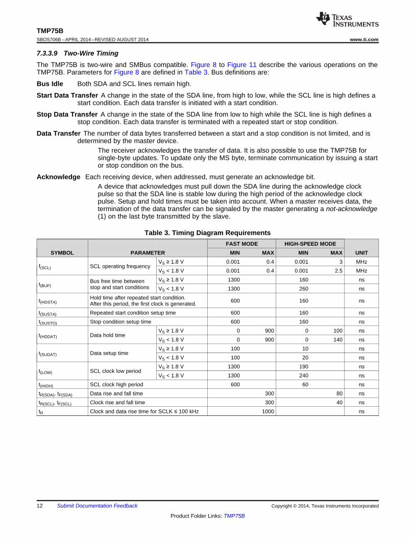
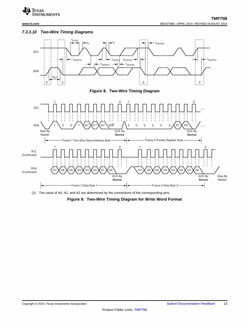
7.3.3.9 Two-Wire TimingThe TMP75B is two-wire and SMBus compatible. Figure 8 to Figure 11 describe the various operations on theTMP75B. Parameters for Figure 8 are defined in Table 3. Bus definitions are:
Bus Idle Both SDA and SCL lines remain high.
Start Data Transfer A change in the state of the SDA line, from high to low, while the SCL line is high defines astart condition. Each data transfer is initiated with a start condition.
Stop Data Transfer A change in the state of the SDA line from low to high while the SCL line is high defines astop condition. Each data transfer is terminated with a repeated start or stop condition.
Data Transfer The number of data bytes transferred between a start and a stop condition is not limited, and isdetermined by the master device.
The receiver acknowledges the transfer of data. It is also possible to use the TMP75B forsingle-byte updates. To update only the MS byte, terminate communication by issuing a startor stop condition on the bus.
Acknowledge Each receiving device, when addressed, must generate an acknowledge bit.A device that acknowledges must pull down the SDA line during the acknowledge clockpulse so that the SDA line is stable low during the high period of the acknowledge clockpulse. Setup and hold times must be taken into account. When a master receives data, thetermination of the data transfer can be signaled by the master generating a not-acknowledge(1) on the last byte transmitted by the slave.
Table 3. Timing Diagram RequirementsFAST MODE HIGH-SPEED MODE
SYMBOL PARAMETER MIN MAX MIN MAX UNITVS ≥ 1.8 V 0.001 0.4 0.001 3 MHz
f(SCL) SCL operating frequencyVS < 1.8 V 0.001 0.4 0.001 2.5 MHzVS ≥ 1.8 V 1300 160 nsBus free time betweent(BUF) stop and start conditions VS < 1.8 V 1300 260 ns
Hold time after repeated start condition.t(HDSTA) 600 160 nsAfter this period, the first clock is generated.t(SUSTA) Repeated start condition setup time 600 160 nst(SUSTO) Stop condition setup time 600 160 ns
VS ≥ 1.8 V 0 900 0 100 nst(HDDAT) Data hold time
VS < 1.8 V 0 900 0 140 nsVS ≥ 1.8 V 100 10 ns
t(SUDAT) Data setup timeVS < 1.8 V 100 20 nsVS ≥ 1.8 V 1300 190 ns
t(LOW) SCL clock low periodVS < 1.8 V 1300 240 ns
t(HIGH) SCL clock high period 600 60 nstR(SDA), tF(SDA) Data rise and fall time 300 80 nstR(SCL), tF(SCL) Clock rise and fall time 300 40 nstR Clock and data rise time for SCLK ≤ 100 kHz 1000 ns
12 Submit Documentation Feedback Copyright © 2014, Texas Instruments Incorporated
Product Folder Links: TMP75B
Frame 1 Two-Wire Slave Address Byte Frame 2 Pointer Register Byte
Frame 4 Data Byte 2
1
Start By
Master
ACK By
Device
ACK By
Device
ACK By
Device
Stop By
Master
1 9 1
1
D7 D6 D5 D4 D3 D2 D1 D0
9
Frame 3 Data Byte 1
ACK By
Device
1
D7SDA
(Continued)
SCL
(Continued)
D6 D5 D4 D3 D2 D1 D0
9
9
SDA
SCL
0 0 1 A1(1) A0(1) R/W 0 0 0 0 0 0 P1 P0 ¼
¼
A2(1)
SCL
SDA
t(LOW)tR tF t(HDSTA)
t(HDSTA)
t(HDDAT)
t(BUF)
t(SUDAT)
t(HIGH) t(SUSTA) t(SUSTO)
P S S P
TMP75Bwww.ti.com SBOS706B –APRIL 2014–REVISED AUGUST 2014
7.3.3.10 Two-Wire Timing Diagrams
Figure 8. Two-Wire Timing Diagram
(1) The value of A0, A1, and A2 are determined by the connections of the corresponding pins.
Figure 9. Two-Wire Timing Diagram for Write Word Format
Copyright © 2014, Texas Instruments Incorporated Submit Documentation Feedback 13
Product Folder Links: TMP75B

Frame 1 SMBus ALERT Response Address Byte Frame 2 Slave Address From Device
Start By
Master
ACK By
Device
From
Device
NACK By
Master
Stop By
Master
1 9 1 9
SDA
SCL
ALERT
0 0 0 1 1 0 0 R/W 1 0 0 1 StatusA1(1)
A0(1)
A2(1)
Frame 1 Two-Wire Slave Address Byte Frame 2 Pointer Register Byte
1
Start ByMaster
ACK By
Device
ACK By
Device
Frame 3 Two-Wire Slave Address Byte Frame 4 Data Byte 1 Read Register
Start By
Master
ACK By
Device
ACK By
Master(2)
From
Device
1 9 1 9
1 9 1 9
SDA
SCL
0 0 1 R/W 0 0 0 0 0 0 P1 P0
¼
¼
¼
SDA
(Continued)
SCL
(Continued)
SDA
(Continued)
SCL
(Continued)
1 0 0 1
A1(1)
A0(1)
A1(1)
A0(1)
R/W D7 D6 D5 D4 D3 D2 D1 D0
Frame 5 Data Byte 2 Read Register
Stop By
Master
ACK By
Master(3)
From
Device
1 9
D7 D6 D5 D4 D3 D2 D1 D0
Stop ByMaster
A2(1)
A2(1)
TMP75BSBOS706B –APRIL 2014–REVISED AUGUST 2014 www.ti.com
(1) The value of A0, A1, and A2 are determined by the connections of the corresponding pins.(2) Master should leave SDA high to terminate a single-byte read operation.(3) Master should leave SDA high to terminate a two-byte read operation.
Figure 10. Two-Wire Timing Diagram for Read Word Format
(1) The value of A0, A1, and A2 are determined by the connections of the corresponding pins.
Figure 11. Timing Diagram for SMBus Alert
14 Submit Documentation Feedback Copyright © 2014, Texas Instruments Incorporated
Product Folder Links: TMP75B
Startup Start ofConversion
Delay(1)
27 ms
Start ofConversion
Delay(1)
27 ms
27 ms
TMP75Bwww.ti.com SBOS706B –APRIL 2014–REVISED AUGUST 2014
7.4 Device Functional Modes
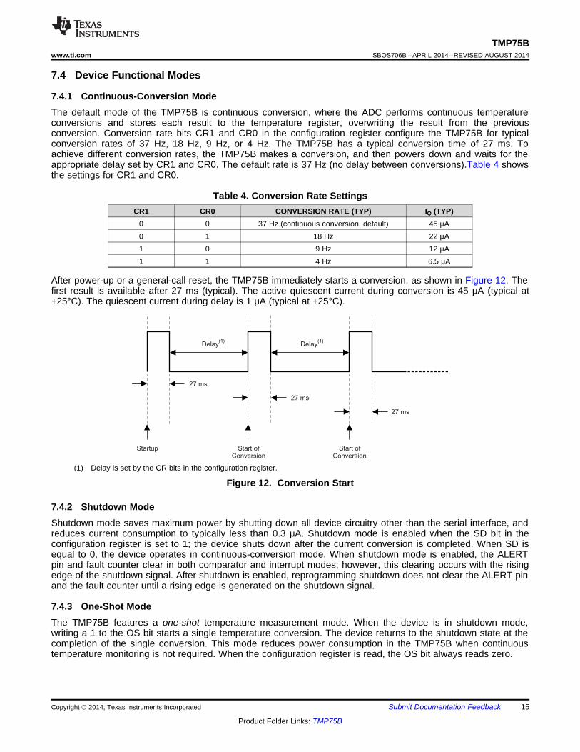
7.4.1 Continuous-Conversion ModeThe default mode of the TMP75B is continuous conversion, where the ADC performs continuous temperatureconversions and stores each result to the temperature register, overwriting the result from the previousconversion. Conversion rate bits CR1 and CR0 in the configuration register configure the TMP75B for typicalconversion rates of 37 Hz, 18 Hz, 9 Hz, or 4 Hz. The TMP75B has a typical conversion time of 27 ms. Toachieve different conversion rates, the TMP75B makes a conversion, and then powers down and waits for theappropriate delay set by CR1 and CR0. The default rate is 37 Hz (no delay between conversions).Table 4 showsthe settings for CR1 and CR0.
Table 4. Conversion Rate SettingsCR1 CR0 CONVERSION RATE (TYP) IQ (TYP)
0 0 37 Hz (continuous conversion, default) 45 μA0 1 18 Hz 22 μA1 0 9 Hz 12 μA1 1 4 Hz 6.5 μA
After power-up or a general-call reset, the TMP75B immediately starts a conversion, as shown in Figure 12. Thefirst result is available after 27 ms (typical). The active quiescent current during conversion is 45 μA (typical at+25°C). The quiescent current during delay is 1 μA (typical at +25°C).
(1) Delay is set by the CR bits in the configuration register.
Figure 12. Conversion Start
7.4.2 Shutdown ModeShutdown mode saves maximum power by shutting down all device circuitry other than the serial interface, andreduces current consumption to typically less than 0.3 μA. Shutdown mode is enabled when the SD bit in theconfiguration register is set to 1; the device shuts down after the current conversion is completed. When SD isequal to 0, the device operates in continuous-conversion mode. When shutdown mode is enabled, the ALERTpin and fault counter clear in both comparator and interrupt modes; however, this clearing occurs with the risingedge of the shutdown signal. After shutdown is enabled, reprogramming shutdown does not clear the ALERT pinand the fault counter until a rising edge is generated on the shutdown signal.
7.4.3 One-Shot ModeThe TMP75B features a one-shot temperature measurement mode. When the device is in shutdown mode,writing a 1 to the OS bit starts a single temperature conversion. The device returns to the shutdown state at thecompletion of the single conversion. This mode reduces power consumption in the TMP75B when continuoustemperature monitoring is not required. When the configuration register is read, the OS bit always reads zero.
Copyright © 2014, Texas Instruments Incorporated Submit Documentation Feedback 15
Product Folder Links: TMP75B

I/O
Control
Interface
SCL
SDA
Temperature
Register
Configuration
Register
TLOW
Register
THIGH
Register
Pointer
Register
TMP75BSBOS706B –APRIL 2014–REVISED AUGUST 2014 www.ti.com
7.5 Programming
Figure 13 shows the internal register structure of the TMP75B. Use the 8-bit pointer register to address a givendata register. The pointer register uses the two LSBs to identify which of the data registers respond to a read orwrite command. Figure 14 identifies the bits of the pointer register byte.
Figure 13. Internal Register Structure
7.6 Register MapTable 5 describes the registers available in the TMP75B with their pointer addresses, followed by the descriptionof the bits in each register.
Table 5. Register Map and Pointer AddressesP1 P0 REGISTER0 0 Temperature register (read only, default)0 1 Configuration register (read/write)1 0 TLOW register (read/write)1 1 THIGH register (read/write)
Figure 14. Pointer Register (pointer = N/A) [reset = 00h]
7 6 5 4 3 2 1 0Reserved P1 P0
W-0h W-0h W-0hLEGEND: R/W = Read/Write; R = Read only; W = Write only; -n = value after reset
16 Submit Documentation Feedback Copyright © 2014, Texas Instruments Incorporated
Product Folder Links: TMP75B
TMP75Bwww.ti.com SBOS706B –APRIL 2014–REVISED AUGUST 2014
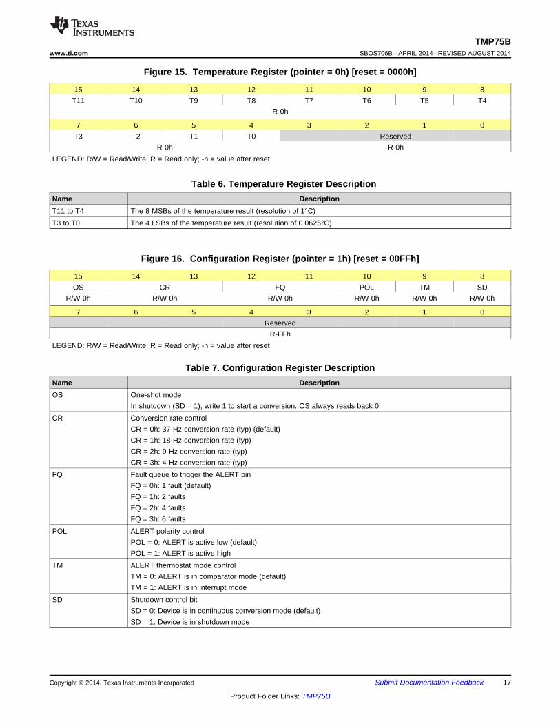
Figure 15. Temperature Register (pointer = 0h) [reset = 0000h]
15 14 13 12 11 10 9 8T11 T10 T9 T8 T7 T6 T5 T4
R-0h
7 6 5 4 3 2 1 0T3 T2 T1 T0 Reserved
R-0h R-0hLEGEND: R/W = Read/Write; R = Read only; -n = value after reset
Table 6. Temperature Register DescriptionName DescriptionT11 to T4 The 8 MSBs of the temperature result (resolution of 1°C)T3 to T0 The 4 LSBs of the temperature result (resolution of 0.0625°C)
Figure 16. Configuration Register (pointer = 1h) [reset = 00FFh]
15 14 13 12 11 10 9 8OS CR FQ POL TM SD
R/W-0h R/W-0h R/W-0h R/W-0h R/W-0h R/W-0h
7 6 5 4 3 2 1 0Reserved
R-FFhLEGEND: R/W = Read/Write; R = Read only; -n = value after reset
Table 7. Configuration Register DescriptionName DescriptionOS One-shot mode
In shutdown (SD = 1), write 1 to start a conversion. OS always reads back 0.CR Conversion rate control
CR = 0h: 37-Hz conversion rate (typ) (default)CR = 1h: 18-Hz conversion rate (typ)CR = 2h: 9-Hz conversion rate (typ)CR = 3h: 4-Hz conversion rate (typ)
FQ Fault queue to trigger the ALERT pinFQ = 0h: 1 fault (default)FQ = 1h: 2 faultsFQ = 2h: 4 faultsFQ = 3h: 6 faults
POL ALERT polarity controlPOL = 0: ALERT is active low (default)POL = 1: ALERT is active high
TM ALERT thermostat mode controlTM = 0: ALERT is in comparator mode (default)TM = 1: ALERT is in interrupt mode
SD Shutdown control bitSD = 0: Device is in continuous conversion mode (default)SD = 1: Device is in shutdown mode
Copyright © 2014, Texas Instruments Incorporated Submit Documentation Feedback 17
Product Folder Links: TMP75B

TMP75BSBOS706B –APRIL 2014–REVISED AUGUST 2014 www.ti.com
Figure 17. TLOW - Temperature Low Limit Register (pointer = 2h) [reset = 4B00h] (1)
15 14 13 12 11 10 9 8L11 L10 L9 L8 L7 L6 L5 L4
R/W-4Bh
7 6 5 4 3 2 1 0L3 L2 L1 L0 Reserved
R/W-0h R-0hLEGEND: R/W = Read/Write; R = Read only; -n = value after reset
(1) 4B00h = 75°C.
Table 8. TLOW Register DescriptionName DescriptionL11 to L4 The 8 MSBs of the temperature low limit (resolution of 1°C)L3 to L0 The 4 LSBs of the temperature low limit (resolution of 0.0625°C)
Figure 18. THIGH - Temperature High Limit Register (pointer = 3h) [reset = 5000h] (1)
15 14 13 12 11 10 9 8H11 H10 H9 H8 H7 H6 H5 H4
R/W-50h
7 6 5 4 3 2 1 0H3 H2 H1 H0 Reserved
R/W-0h R-0hLEGEND: R/W = Read/Write; R = Read only; -n = value after reset
(1) 5000h = 80°C.
Table 9. THIGH Register DescriptionName DescriptionH11 to H4 The 8 MSBs of the temperature high limit (resolution of 1°C)H3 to H0 The 4 LSBs of the temperature high limit (resolution of 0.0625°C)
18 Submit Documentation Feedback Copyright © 2014, Texas Instruments Incorporated
Product Folder Links: TMP75B

A2
SDA
SCL
GND
ALERT
2
6
8
7
1
A1
A0
VS
4
3
5
0.01 PF
Two-WireHost Controller
TMP75B
1.4 V to 3.6 V
A2
SDA
SCL
GND
ALERT
2
6
8
7
1
A1
A0
VS
4
3
5
0.01 PFTMP75B
1.4 V to 3.6 V
Connect to VS or GND for up to 8 Address Combinations
Connect to VS or GND for up to 8 Address Combinations
Additional Sensor
Locations
TMP75Bwww.ti.com SBOS706B –APRIL 2014–REVISED AUGUST 2014
8 Application and Implementation
8.1 Application InformationThe TMP75B is used to measure the PCB temperature of the location it is mounted. The programmable addressoptions allow up to eight locations on the board to be monitored on a single serial bus. Connecting the ALERTpins together and programming the temperature limit registers to desired values allows for a temperaturewatchdog operation of all devices, interrupting the host controller only if the temperature exceeds the limits.
8.2 Typical Application
Figure 19. Temperature Monitoring of Multiple Locations on a PCB
Copyright © 2014, Texas Instruments Incorporated Submit Documentation Feedback 19
Product Folder Links: TMP75B

25 30 35 40 45 50 55 60 65 70 75 80 85 90 95
100
±1 0 1 2 3 4 5 6 7 8 9 10 11 12 13 14 15 16 17 18 19 20
Tem
pera
ture
(�C
)
Time (s) C007
TMP75BSBOS706B –APRIL 2014–REVISED AUGUST 2014 www.ti.com
Typical Application (continued)8.2.1 Design RequirementsThe TMP75B only requires pull-up resistors on SDA and ALERT, although a pull-up resistor is typically presenton the SCL as well. A 0.01-μF bypass capacitor on the supply is recommended, as shown in Figure 19. TheSCL, SDA, and ALERT lines can be pulled up to a supply that is equal to or higher than VS through the pull-upresistors. To configure one of eight different addresses on the bus, connect A0, A1, and A2 to either VS or GND.
8.2.2 Detailed Design ProcedureThe TMP75B should be placed in close proximity to the heat source to be monitored, with a proper layout forgood thermal coupling. This ensures that temperature changes are captured within the shortest possible timeinterval.
8.2.3 Application CurvesFigure 20 shows the step response of the TMP75B to a submersion in an oil bath of 100°C from roomtemperature (27°C). The time-constant, or the time for the output to reach 63% of the input step, is 1.5 seconds.
Figure 20. Temperature Step Response
9 Power Supply RecommendationsThe TMP75B operates with power supply in the range of 1.4 V to 3.6 V. It is optimized for operation at 1.8-Vsupply but can measure temperature accurately in the full supply range.
A power-supply bypass capacitor is required for stability; place this capacitor as close as possible to the supplyand ground pins of the device. A typical value for this supply bypass capacitor is 0.01 μF. Applications with noisyor high-impedance power supplies may require additional decoupling capacitors to reject power-supply noise.
20 Submit Documentation Feedback Copyright © 2014, Texas Instruments Incorporated
Product Folder Links: TMP75B
Serial Bus Traces
Pull-Up ResistorsSupply Bypass
Capacitor
Via to Power or Ground Plane
Via to Internal Layer
Supply VoltageSDA
SCL
ALERT
A2
A1
A0
VS
GND
Ground Plane forThermal Coupling
to Heat Source
Heat Source
TMP75Bwww.ti.com SBOS706B –APRIL 2014–REVISED AUGUST 2014
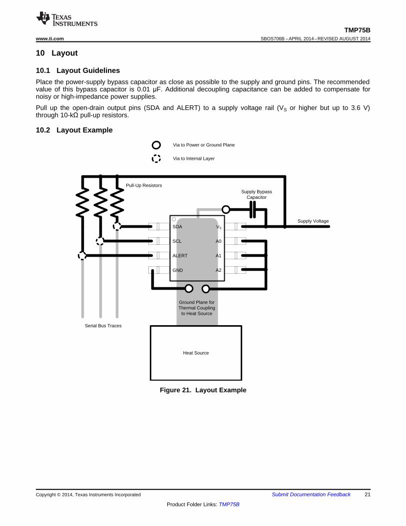
10 Layout
10.1 Layout GuidelinesPlace the power-supply bypass capacitor as close as possible to the supply and ground pins. The recommendedvalue of this bypass capacitor is 0.01 μF. Additional decoupling capacitance can be added to compensate fornoisy or high-impedance power supplies.
Pull up the open-drain output pins (SDA and ALERT) to a supply voltage rail (VS or higher but up to 3.6 V)through 10-kΩ pull-up resistors.
10.2 Layout Example
Figure 21. Layout Example
Copyright © 2014, Texas Instruments Incorporated Submit Documentation Feedback 21
Product Folder Links: TMP75B
TMP75BSBOS706B –APRIL 2014–REVISED AUGUST 2014 www.ti.com
11 Device and Documentation Support
11.1 Documentation Support
11.1.1 Related DocumentationSBOU141 — TMP75xEVM User's Guide
11.2 TrademarksAll trademarks are the property of their respective owners.
11.3 Electrostatic Discharge CautionThese devices have limited built-in ESD protection. The leads should be shorted together or the device placed in conductive foamduring storage or handling to prevent electrostatic damage to the MOS gates.
11.4 GlossarySLYZ022 — TI Glossary.
This glossary lists and explains terms, acronyms, and definitions.
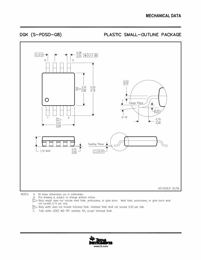
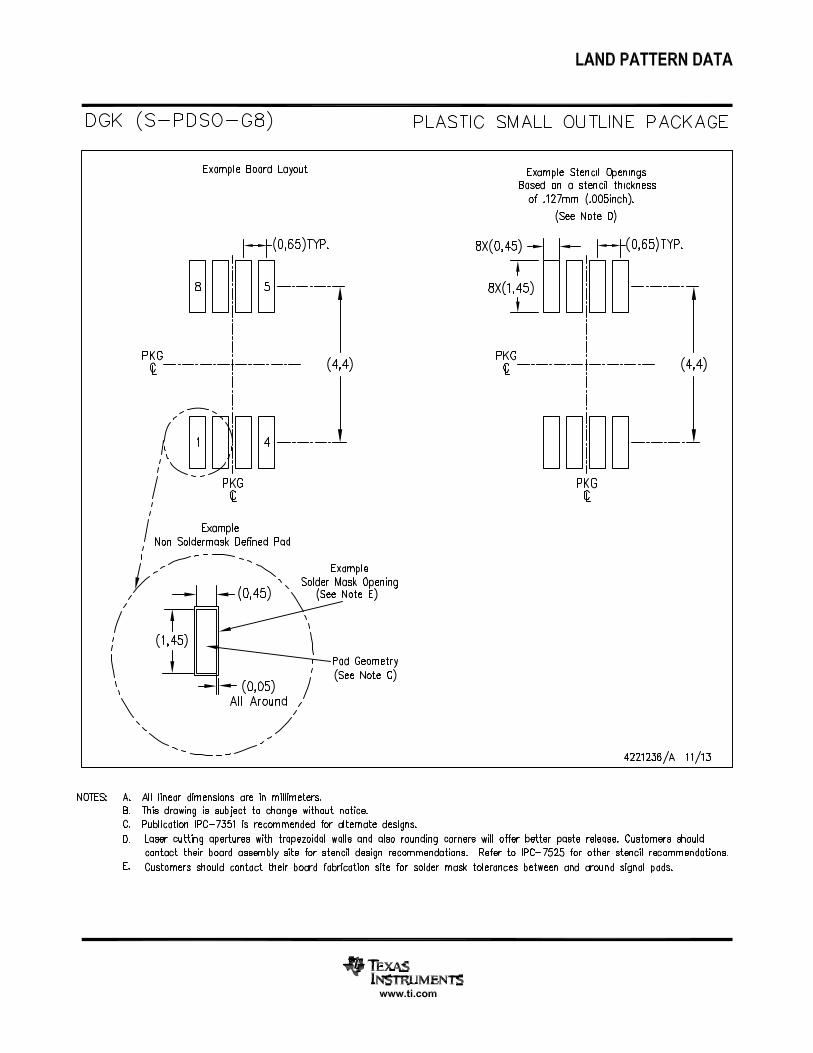
12 Mechanical, Packaging, and Orderable InformationThe following pages include mechanical, packaging, and orderable information. This information is the mostcurrent data available for the designated devices. This data is subject to change without notice and revision ofthis document. For browser-based versions of this data sheet, refer to the left-hand navigation.
22 Submit Documentation Feedback Copyright © 2014, Texas Instruments Incorporated
Product Folder Links: TMP75B

PACKAGE OPTION ADDENDUM
www.ti.com 11-Apr-2015
Addendum-Page 1
PACKAGING INFORMATION
Orderable Device Status(1)
Package Type PackageDrawing
Pins PackageQty
Eco Plan(2)
Lead/Ball Finish(6)
MSL Peak Temp(3)
Op Temp (°C) Device Marking(4/5)
Samples
TMP75BID ACTIVE SOIC D 8 75 Green (RoHS& no Sb/Br)
CU NIPDAU-DCC Level-1-260C-UNLIM -55 to 125 TMP75B
TMP75BIDGKR ACTIVE VSSOP DGK 8 2500 Green (RoHS& no Sb/Br)
CU NIPDAUAG Level-2-260C-1 YEAR -55 to 125 T75B
TMP75BIDGKT ACTIVE VSSOP DGK 8 250 Green (RoHS& no Sb/Br)
CU NIPDAUAG Level-2-260C-1 YEAR -55 to 125 T75B
TMP75BIDR ACTIVE SOIC D 8 2500 Green (RoHS& no Sb/Br)
CU NIPDAU-DCC Level-1-260C-UNLIM -55 to 125 TMP75B
(1) The marketing status values are defined as follows:ACTIVE: Product device recommended for new designs.LIFEBUY: TI has announced that the device will be discontinued, and a lifetime-buy period is in effect.NRND: Not recommended for new designs. Device is in production to support existing customers, but TI does not recommend using this part in a new design.PREVIEW: Device has been announced but is not in production. Samples may or may not be available.OBSOLETE: TI has discontinued the production of the device.
(2) Eco Plan - The planned eco-friendly classification: Pb-Free (RoHS), Pb-Free (RoHS Exempt), or Green (RoHS & no Sb/Br) - please check http://www.ti.com/productcontent for the latest availabilityinformation and additional product content details.TBD: The Pb-Free/Green conversion plan has not been defined.Pb-Free (RoHS): TI's terms "Lead-Free" or "Pb-Free" mean semiconductor products that are compatible with the current RoHS requirements for all 6 substances, including the requirement thatlead not exceed 0.1% by weight in homogeneous materials. Where designed to be soldered at high temperatures, TI Pb-Free products are suitable for use in specified lead-free processes.Pb-Free (RoHS Exempt): This component has a RoHS exemption for either 1) lead-based flip-chip solder bumps used between the die and package, or 2) lead-based die adhesive used betweenthe die and leadframe. The component is otherwise considered Pb-Free (RoHS compatible) as defined above.Green (RoHS & no Sb/Br): TI defines "Green" to mean Pb-Free (RoHS compatible), and free of Bromine (Br) and Antimony (Sb) based flame retardants (Br or Sb do not exceed 0.1% by weightin homogeneous material)
(3) MSL, Peak Temp. - The Moisture Sensitivity Level rating according to the JEDEC industry standard classifications, and peak solder temperature.
(4) There may be additional marking, which relates to the logo, the lot trace code information, or the environmental category on the device.
(5) Multiple Device Markings will be inside parentheses. Only one Device Marking contained in parentheses and separated by a "~" will appear on a device. If a line is indented then it is a continuationof the previous line and the two combined represent the entire Device Marking for that device.
(6) Lead/Ball Finish - Orderable Devices may have multiple material finish options. Finish options are separated by a vertical ruled line. Lead/Ball Finish values may wrap to two lines if the finishvalue exceeds the maximum column width.
PACKAGE OPTION ADDENDUM
www.ti.com 11-Apr-2015
Addendum-Page 2
Important Information and Disclaimer:The information provided on this page represents TI's knowledge and belief as of the date that it is provided. TI bases its knowledge and belief on informationprovided by third parties, and makes no representation or warranty as to the accuracy of such information. Efforts are underway to better integrate information from third parties. TI has taken andcontinues to take reasonable steps to provide representative and accurate information but may not have conducted destructive testing or chemical analysis on incoming materials and chemicals.TI and TI suppliers consider certain information to be proprietary, and thus CAS numbers and other limited information may not be available for release.
In no event shall TI's liability arising out of such information exceed the total purchase price of the TI part(s) at issue in this document sold by TI to Customer on an annual basis.
OTHER QUALIFIED VERSIONS OF TMP75B :
• Automotive: TMP75B-Q1
NOTE: Qualified Version Definitions:
• Automotive - Q100 devices qualified for high-reliability automotive applications targeting zero defects
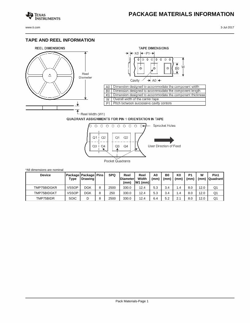
TAPE AND REEL INFORMATION
*All dimensions are nominal
Device PackageType
PackageDrawing
Pins SPQ ReelDiameter
(mm)
ReelWidth
W1 (mm)
A0(mm)
B0(mm)
K0(mm)
P1(mm)
W(mm)
Pin1Quadrant
TMP75BIDGKR VSSOP DGK 8 2500 330.0 12.4 5.3 3.4 1.4 8.0 12.0 Q1
TMP75BIDGKT VSSOP DGK 8 250 330.0 12.4 5.3 3.4 1.4 8.0 12.0 Q1
TMP75BIDR SOIC D 8 2500 330.0 12.4 6.4 5.2 2.1 8.0 12.0 Q1
PACKAGE MATERIALS INFORMATION
www.ti.com 3-Jul-2017
Pack Materials-Page 1

*All dimensions are nominal
Device Package Type Package Drawing Pins SPQ Length (mm) Width (mm) Height (mm)
TMP75BIDGKR VSSOP DGK 8 2500 366.0 364.0 50.0
TMP75BIDGKT VSSOP DGK 8 250 366.0 364.0 50.0
TMP75BIDR SOIC D 8 2500 367.0 367.0 35.0
PACKAGE MATERIALS INFORMATION
www.ti.com 3-Jul-2017
Pack Materials-Page 2


IMPORTANT NOTICE
Texas Instruments Incorporated (TI) reserves the right to make corrections, enhancements, improvements and other changes to itssemiconductor products and services per JESD46, latest issue, and to discontinue any product or service per JESD48, latest issue. Buyersshould obtain the latest relevant information before placing orders and should verify that such information is current and complete.TI’s published terms of sale for semiconductor products (http://www.ti.com/sc/docs/stdterms.htm) apply to the sale of packaged integratedcircuit products that TI has qualified and released to market. Additional terms may apply to the use or sale of other types of TI products andservices.Reproduction of significant portions of TI information in TI data sheets is permissible only if reproduction is without alteration and isaccompanied by all associated warranties, conditions, limitations, and notices. TI is not responsible or liable for such reproduceddocumentation. Information of third parties may be subject to additional restrictions. Resale of TI products or services with statementsdifferent from or beyond the parameters stated by TI for that product or service voids all express and any implied warranties for theassociated TI product or service and is an unfair and deceptive business practice. TI is not responsible or liable for any such statements.Buyers and others who are developing systems that incorporate TI products (collectively, “Designers”) understand and agree that Designersremain responsible for using their independent analysis, evaluation and judgment in designing their applications and that Designers havefull and exclusive responsibility to assure the safety of Designers' applications and compliance of their applications (and of all TI productsused in or for Designers’ applications) with all applicable regulations, laws and other applicable requirements. Designer represents that, withrespect to their applications, Designer has all the necessary expertise to create and implement safeguards that (1) anticipate dangerousconsequences of failures, (2) monitor failures and their consequences, and (3) lessen the likelihood of failures that might cause harm andtake appropriate actions. Designer agrees that prior to using or distributing any applications that include TI products, Designer willthoroughly test such applications and the functionality of such TI products as used in such applications.TI’s provision of technical, application or other design advice, quality characterization, reliability data or other services or information,including, but not limited to, reference designs and materials relating to evaluation modules, (collectively, “TI Resources”) are intended toassist designers who are developing applications that incorporate TI products; by downloading, accessing or using TI Resources in anyway, Designer (individually or, if Designer is acting on behalf of a company, Designer’s company) agrees to use any particular TI Resourcesolely for this purpose and subject to the terms of this Notice.TI’s provision of TI Resources does not expand or otherwise alter TI’s applicable published warranties or warranty disclaimers for TIproducts, and no additional obligations or liabilities arise from TI providing such TI Resources. TI reserves the right to make corrections,enhancements, improvements and other changes to its TI Resources. TI has not conducted any testing other than that specificallydescribed in the published documentation for a particular TI Resource.Designer is authorized to use, copy and modify any individual TI Resource only in connection with the development of applications thatinclude the TI product(s) identified in such TI Resource. NO OTHER LICENSE, EXPRESS OR IMPLIED, BY ESTOPPEL OR OTHERWISETO ANY OTHER TI INTELLECTUAL PROPERTY RIGHT, AND NO LICENSE TO ANY TECHNOLOGY OR INTELLECTUAL PROPERTYRIGHT OF TI OR ANY THIRD PARTY IS GRANTED HEREIN, including but not limited to any patent right, copyright, mask work right, orother intellectual property right relating to any combination, machine, or process in which TI products or services are used. Informationregarding or referencing third-party products or services does not constitute a license to use such products or services, or a warranty orendorsement thereof. Use of TI Resources may require a license from a third party under the patents or other intellectual property of thethird party, or a license from TI under the patents or other intellectual property of TI.TI RESOURCES ARE PROVIDED “AS IS” AND WITH ALL FAULTS. TI DISCLAIMS ALL OTHER WARRANTIES ORREPRESENTATIONS, EXPRESS OR IMPLIED, REGARDING RESOURCES OR USE THEREOF, INCLUDING BUT NOT LIMITED TOACCURACY OR COMPLETENESS, TITLE, ANY EPIDEMIC FAILURE WARRANTY AND ANY IMPLIED WARRANTIES OFMERCHANTABILITY, FITNESS FOR A PARTICULAR PURPOSE, AND NON-INFRINGEMENT OF ANY THIRD PARTY INTELLECTUALPROPERTY RIGHTS. TI SHALL NOT BE LIABLE FOR AND SHALL NOT DEFEND OR INDEMNIFY DESIGNER AGAINST ANY CLAIM,INCLUDING BUT NOT LIMITED TO ANY INFRINGEMENT CLAIM THAT RELATES TO OR IS BASED ON ANY COMBINATION OFPRODUCTS EVEN IF DESCRIBED IN TI RESOURCES OR OTHERWISE. IN NO EVENT SHALL TI BE LIABLE FOR ANY ACTUAL,DIRECT, SPECIAL, COLLATERAL, INDIRECT, PUNITIVE, INCIDENTAL, CONSEQUENTIAL OR EXEMPLARY DAMAGES INCONNECTION WITH OR ARISING OUT OF TI RESOURCES OR USE THEREOF, AND REGARDLESS OF WHETHER TI HAS BEENADVISED OF THE POSSIBILITY OF SUCH DAMAGES.Unless TI has explicitly designated an individual product as meeting the requirements of a particular industry standard (e.g., ISO/TS 16949and ISO 26262), TI is not responsible for any failure to meet such industry standard requirements.Where TI specifically promotes products as facilitating functional safety or as compliant with industry functional safety standards, suchproducts are intended to help enable customers to design and create their own applications that meet applicable functional safety standardsand requirements. Using products in an application does not by itself establish any safety features in the application. Designers mustensure compliance with safety-related requirements and standards applicable to their applications. Designer may not use any TI products inlife-critical medical equipment unless authorized officers of the parties have executed a special contract specifically governing such use.Life-critical medical equipment is medical equipment where failure of such equipment would cause serious bodily injury or death (e.g., lifesupport, pacemakers, defibrillators, heart pumps, neurostimulators, and implantables). Such equipment includes, without limitation, allmedical devices identified by the U.S. Food and Drug Administration as Class III devices and equivalent classifications outside the U.S.TI may expressly designate certain products as completing a particular qualification (e.g., Q100, Military Grade, or Enhanced Product).Designers agree that it has the necessary expertise to select the product with the appropriate qualification designation for their applicationsand that proper product selection is at Designers’ own risk. Designers are solely responsible for compliance with all legal and regulatoryrequirements in connection with such selection.Designer will fully indemnify TI and its representatives against any damages, costs, losses, and/or liabilities arising out of Designer’s non-compliance with the terms and provisions of this Notice.
Mailing Address: Texas Instruments, Post Office Box 655303, Dallas, Texas 75265Copyright © 2017, Texas Instruments Incorporated