Digital Systems Design - University of...
14
1 Dr. D. J. Jackson Lecture 9-1 Electrical & Computer Engineering Digital Systems Design Clock Networks and Phase Lock Loops on Altera Cyclone V Devices Dr. D. J. Jackson Lecture 9-2 Electrical & Computer Engineering Global Clock Network & Phase-Locked Loops • Clock management is important within digital systems design – High speed designs require low latency, low skew clock solutions • Low latency – a minimum propagation delay time throughout the device • Low skew – a minimum difference between actual clock edges as seen on various points on the device – Sources for clock skew? » Propagation delay through the device, capacitive loading • Cyclone V devices provide the following for clock management – Global, regional, and periphery clock networks – Multiple phase-locked loops (PLLs)
Transcript of Digital Systems Design - University of...

1
Dr. D. J. Jackson Lecture 9-1Electrical & Computer Engineering
Digital Systems Design
Clock Networks and Phase Lock Loops on Altera Cyclone V Devices
Dr. D. J. Jackson Lecture 9-2Electrical & Computer Engineering
Global Clock Network & Phase-Locked Loops
• Clock management is important within digital systems design– High speed designs require low latency, low skew clock
solutions• Low latency – a minimum propagation delay time throughout the
device• Low skew – a minimum difference between actual clock edges as
seen on various points on the device– Sources for clock skew?
» Propagation delay through the device, capacitive loading
• Cyclone V devices provide the following for clock management– Global, regional, and periphery clock networks– Multiple phase-locked loops (PLLs)

2
Dr. D. J. Jackson Lecture 9-3Electrical & Computer Engineering
Phase-Locked Loops (PLLs)
• A PLL is a closed-loop feedback control system that maintains a generated signal in a fixed phase relationship to a reference signal
• Applications include:– Frequency synthesizers for digitally-tuned radio receivers and
transmitters
– FM and AM radio signal demodulation
– Clock multipliers in digital systems that allow internal elements to run faster (or slower) than external connections, while maintaining precise timing relationships (our basic application in this course)
• Cyclone V PLLs provide general-purpose clocking with clock multiplication (or division) and phase shifting
Dr. D. J. Jackson Lecture 9-4Electrical & Computer Engineering
Typical PLL Architecture

3
Dr. D. J. Jackson Lecture 9-5Electrical & Computer Engineering
Cyclone V PLLs
• Cyclone V device family contains fractional PLLs that can function as fractional PLLs or integer PLLs
• Provide robust clock management and synthesis for device clock management, and external system clock management
• PLLs offer clock– Frequency multiplication and division– Phase shifting– Programmable duty cycle– Multiple modes of operation
• We will only address one simple mode of operation for our purposes
Dr. D. J. Jackson Lecture 9-6Electrical & Computer Engineering
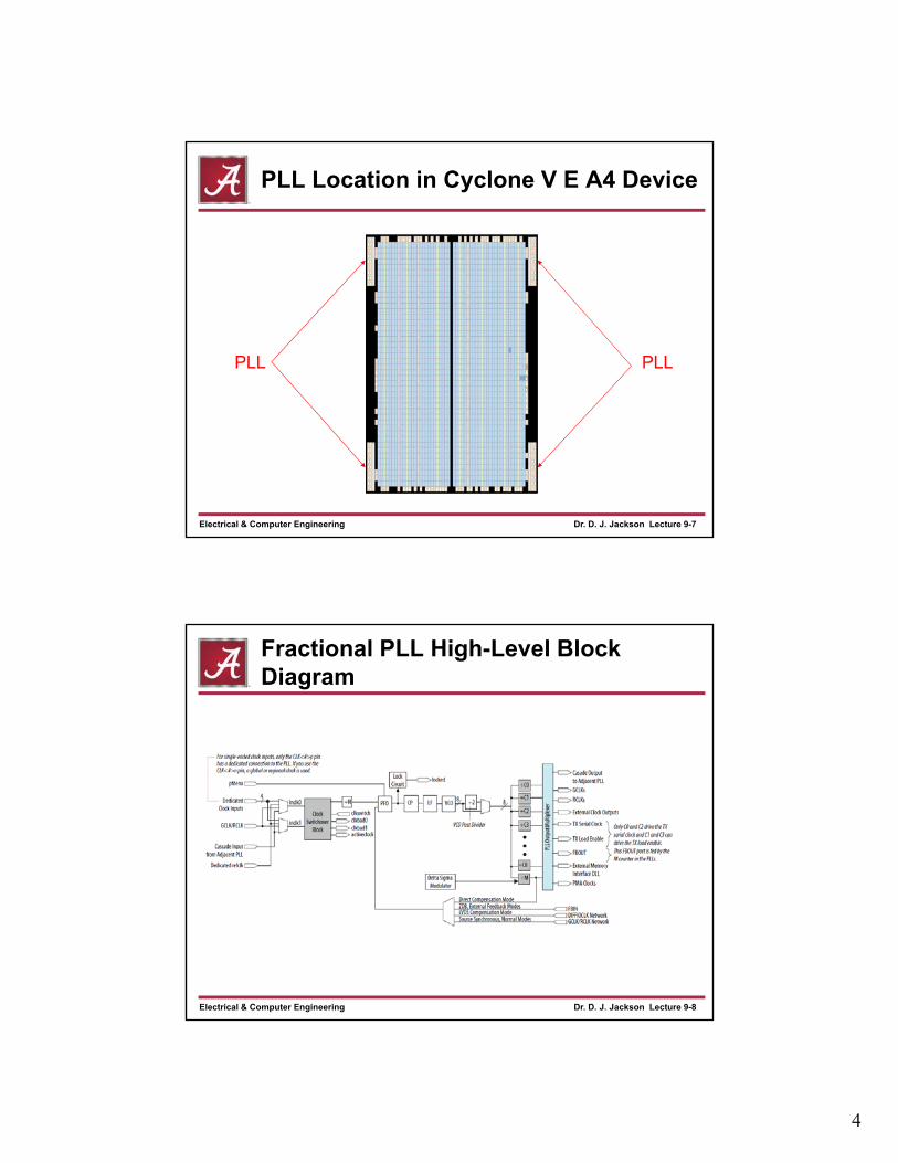
PLL Location in Cyclone V E A4 Device
4
Dr. D. J. Jackson Lecture 9-7Electrical & Computer Engineering
PLL Location in Cyclone V E A4 Device
PLL PLL
Dr. D. J. Jackson Lecture 9-8Electrical & Computer Engineering
Fractional PLL High-Level Block Diagram

5
Dr. D. J. Jackson Lecture 9-9Electrical & Computer Engineering
Fractional PLL Usage
• You can configure the fractional PLL to function either in the integer or in the enhanced fractional mode
• One fractional PLL can use up to 9 output counters and all external clock outputs
• Fractional PLLs can be used as follows:– Reduce the number of required oscillators on the board
– Reduce the clock pins used in the FPGA by synthesizing multiple clock frequencies from a single reference clock source
– Compensate clock network delay
– Zero delay buffering
– Transmit clocking for transceivers
Dr. D. J. Jackson Lecture 9-10Electrical & Computer Engineering
PLL Cascading
• Cyclone V devices support two types of PLL cascading
• PLL-to-PLL Cascading– This cascading mode synthesizes a more precise output frequency
than a single PLL in integer mode
– Cascading two PLLs in integer mode expands the effective range of the pre-scale counter, N and the multiply counter, M
• Counter-Output-to-Counter-Output Cascading– This cascading mode synthesizes a lower frequency output than a
single post-scale counter, C
– Cascading two C counters expands the effective range of C counters
6
Dr. D. J. Jackson Lecture 9-11Electrical & Computer Engineering
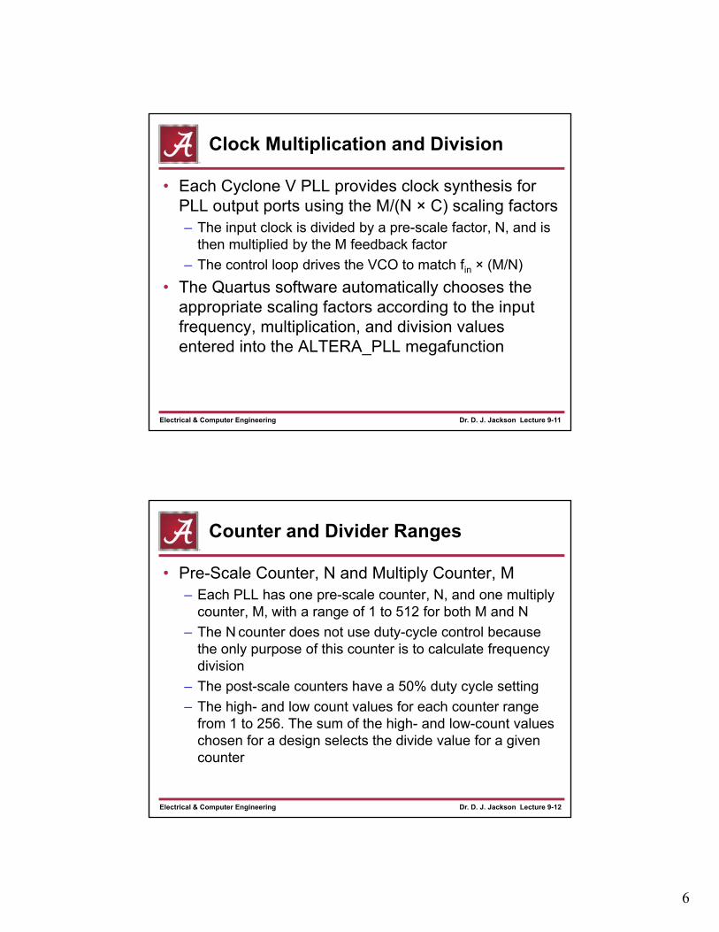
Clock Multiplication and Division
• Each Cyclone V PLL provides clock synthesis for PLL output ports using the M/(N × C) scaling factors– The input clock is divided by a pre-scale factor, N, and is
then multiplied by the M feedback factor
– The control loop drives the VCO to match fin × (M/N)
• The Quartus software automatically chooses the appropriate scaling factors according to the input frequency, multiplication, and division values entered into the ALTERA_PLL megafunction
Dr. D. J. Jackson Lecture 9-12Electrical & Computer Engineering
Counter and Divider Ranges
• Pre-Scale Counter, N and Multiply Counter, M– Each PLL has one pre-scale counter, N, and one multiply
counter, M, with a range of 1 to 512 for both M and N
– The N counter does not use duty-cycle control because the only purpose of this counter is to calculate frequency division
– The post-scale counters have a 50% duty cycle setting
– The high- and low count values for each counter range from 1 to 256. The sum of the high- and low-count values chosen for a design selects the divide value for a given counter

7
Dr. D. J. Jackson Lecture 9-13Electrical & Computer Engineering
Counter and Divider Ranges
• Fractional Mode– In fractional mode, the M counter divide value equals to
the sum of the "clock high" count, "clock low“ count, and the fractional value
– The fractional value is equal to K/2^X, where K is an integer between 0 and (2^X – 1), and X = 8, 16, 24, or 32
• Integer Mode– For PLL operating in integer mode, M is an integer value
Dr. D. J. Jackson Lecture 9-14Electrical & Computer Engineering
Programmable Phase Shift
• The programmable phase shift feature allows the PLLs to generate output clocks with a fixed phase offset
• The VCO frequency of the PLL determines the precision of the phase shift. The minimum phase shift increment is 1/8 of the VCO period. For example, if a PLL operates with a VCO frequency of 1000 MHz, phase shift steps of 125 ps are possible
• The Quartus software automatically adjusts the VCO frequency according to the user-specified phase shift values entered into the megafunction

8
Dr. D. J. Jackson Lecture 9-15Electrical & Computer Engineering
Programmable Duty Cycle
• The programmable duty cycle allows PLLs to generate clock outputs with a variable duty cycle
• This feature is supported on the PLL post-scale counters
• The duty-cycle setting is achieved by a low and high time-count setting for the post-scale counters
• To determine the duty cycle choices, the Quartus II software uses the frequency input and the required multiply or divide rate
• The post-scale counter value determines the precision of the duty cycle
Dr. D. J. Jackson Lecture 9-16Electrical & Computer Engineering
Clock Networks
• The Cyclone V devices contain the following clock networks that are organized into a hierarchical structure:– Global clock (GCLK) networks
– Regional clock (RCLK) networks
– Periphery clock (PCLK) networks• On some Cyclone V devices (not on the Cyclone V on the DE0-
CV board)
9
Dr. D. J. Jackson Lecture 9-17Electrical & Computer Engineering
Clock Resources in Cyclone V Devices
• For the Cyclone V E A4 device– Clock input pins
• 18 single-ended or 9 differential
• CLK[0..3][p,n], CLK[6][p,n], and CLK[8..11][p,n] pins
• CLOCK_50 is the CLK0p pin on the DE0-CV board
– GCLK and RCLK networks• GCLK networks: 16
• RCLK networks: 88
• Clock sources: CLK[0..3][p,n], CLK[6][p,n], CLK[8..11][p,n] pins, PLL clock outputs, and logic array
Dr. D. J. Jackson Lecture 9-18Electrical & Computer Engineering
Global Clock Networks
• Cyclone V devices provide GCLKs that can drive throughout the device
• The GCLKs serve as low-skew clock sources for functional blocks, such as adaptive logic modules (ALMs), embedded memory, and PLLs
• Cyclone V I/O elements (IOEs) and internal logic can also drive GCLKs to create internally-generated global clocks and other high fan-out control signals, such as synchronous or asynchronous clear and clock enable signals

10
Dr. D. J. Jackson Lecture 9-19Electrical & Computer Engineering
GCLK Networks in Cyclone V E
Dr. D. J. Jackson Lecture 9-20Electrical & Computer Engineering
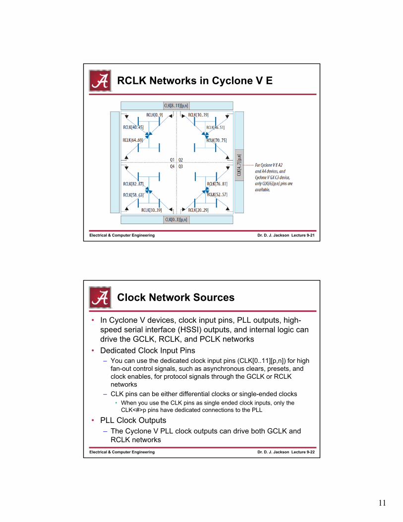
Regional Clock Networks
• RCLK networks are only applicable to the quadrant they drive into
• RCLK networks provide the lowest clock insertion delay and skew for logic contained within a single device quadrant
• The Cyclone V IOEs and internal logic within a given quadrant can also drive RCLKs to create internally generated regional clocks and other high fan-out control signals
11
Dr. D. J. Jackson Lecture 9-21Electrical & Computer Engineering
RCLK Networks in Cyclone V E
Dr. D. J. Jackson Lecture 9-22Electrical & Computer Engineering
Clock Network Sources
• In Cyclone V devices, clock input pins, PLL outputs, high-speed serial interface (HSSI) outputs, and internal logic can drive the GCLK, RCLK, and PCLK networks
• Dedicated Clock Input Pins– You can use the dedicated clock input pins (CLK[0..11][p,n]) for high
fan-out control signals, such as asynchronous clears, presets, and clock enables, for protocol signals through the GCLK or RCLK networks
– CLK pins can be either differential clocks or single-ended clocks• When you use the CLK pins as single ended clock inputs, only the
CLK<#>p pins have dedicated connections to the PLL
• PLL Clock Outputs– The Cyclone V PLL clock outputs can drive both GCLK and
RCLK networks

12
Dr. D. J. Jackson Lecture 9-23Electrical & Computer Engineering
Clock Control Block
• Every GCLK, RCLK, and PCLK network has its own clock control block
• The control block provides the following features:– Clock source selection (dynamic selection available only
for GCLKs)
– Global clock multiplexing
– Clock power down (static or dynamic clock enable or disable available only for GCLKs and RCLKs)
Dr. D. J. Jackson Lecture 9-24Electrical & Computer Engineering
GCLK Control Block for Cyclone V Devices
13
Dr. D. J. Jackson Lecture 9-25Electrical & Computer Engineering
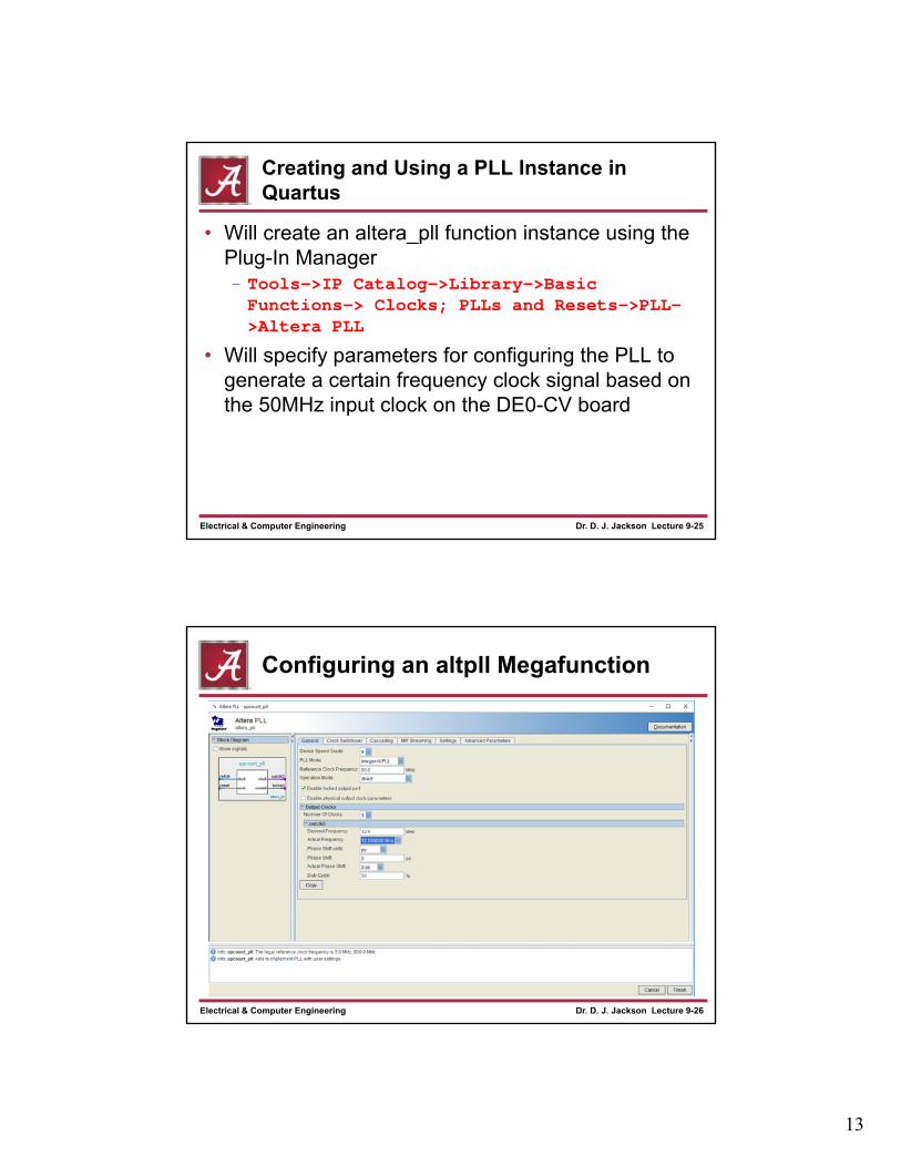
Creating and Using a PLL Instance in Quartus
• Will create an altera_pll function instance using the Plug-In Manager– Tools->IP Catalog->Library->Basic Functions-> Clocks; PLLs and Resets->PLL->Altera PLL
• Will specify parameters for configuring the PLL to generate a certain frequency clock signal based on the 50MHz input clock on the DE0-CV board
Dr. D. J. Jackson Lecture 9-26Electrical & Computer Engineering
Configuring an altpll Megafunction

14
Dr. D. J. Jackson Lecture 9-27Electrical & Computer Engineering
Configuring an altera_pll Megafunction(continued)
• Generates mypll.vhd
• Additional Megawizard screens not shown here since they are not used in this example– Default selections used for all screens not shown
• A Signal Tap II instance can be used to display the generated clock output


![dEVELOP Umavrk WIRELESS sensing system with · PDF fileApplication Note [DEVELOP UMAVRK WIRELESS SENSING SYSTEM WITH CCS] ChaiYong Lim | ECE480 Spring 2012 3 Introduction The UR-CC430F5137-MVK](https://static.fdocuments.in/doc/165x107/5aac519f7f8b9a8d678cbdf7/develop-umavrk-wireless-sensing-system-with-note-develop-umavrk-wireless-sensing.jpg)