Digital IntegratedDigital Integrated Circuits
50
Digital Integrated Digital Integrated Circuits Circuits YuZhuo Fu contact:[email protected] Office location:417 room WeiDianZi building,No 800 DongChuan road,MinHang Campus Digital IC Introduction
Transcript of Digital IntegratedDigital Integrated Circuits

Digital IntegratedDigital Integrated CircuitsCircuits
YuZhuo Fucontact:[email protected]
Office location:417 roomWeiDianZi building,No 800 DongChuan
road,MinHang Campus
Digital ICIntroduction

3.CMOS Inverter
Digital ICIntroduction

outline• CMOS at a glance• CMOS static behavior• CMOS dynamic behavior• Power, Energy, and Energy Delay• Perspective tech.p
Digital IC 3

Dynamic Power Consumptiony p• (dis)charge process
• CL is charged through pMOS on-resistance • CL is discharged through nMOS on-resistance
• Power distribution• Charge processing:One part of Supply power is g p g p pp y p
dissipated in the pMOS transistor,another part is dissipated in the charge CL
• Discharge processing:all dissipated in the nMOS transistor
Digital IC 4

Precise measure of dynamic power cons mptionconsumption
∫ ∫==∞ ∞
dddd
outLddddVV dt
dtdvCVdtVtiE
0 0
)(
∫ ==ddV
ddLoutddL VCdvVC 2
0 0
∫ ddLoutddL0
∫ ∫∞ ∞
out dtdvCdttiE )(∫ ∫==
dd
dd
V
outout
LoutVC
VC
dtvdt
CdtvtiE
2
0 0
)(
∫ ==ddV
ddLoutoutL
VCdvvC0
2
2
Digital IC 5
Output voltages and supply current during (dis)charge of C(dis)charge of CL
• Energy dissipation is independent of the size• Power consumption is dependent of device switching
number.
charge discharge
Digital IC 6

Power and Energy Figures of Meritgy g• Power consumption in Watts
• determines battery life in hours• Peak power
• determines power ground wiring designs• determines power ground wiring designs• sets packaging limits• impacts signal noise margin and reliability analysisp g g y y
• Energy efficiency in Joules• rate at which power is consumed over time
• Energy = power * delay• Joules = Watts * seconds• lower energy number means less power to perform a• lower energy number means less power to perform a
computation at the same frequency
Digital IC
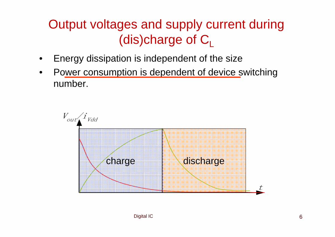
Power versus Energy
Power is height of curveWatts
Power is height of curve
Approach 1
Lower power design could simply be slower
Approach 1
Approach 2
time
WattsEnergy is area under curve
T h i thWatts
Approach 1
Two approaches require the same energy
time
Approach 2
Digital IC

PDP and EDP
Power delay product (PDP) = P * t = (C V 2)/2• Power-delay product (PDP) = Pav * tp = (CLVDD2)/2
• PDP is the average energy consumed per switching event (Watts * sec = Joule)event (Watts sec = Joule)
• lower power design could simply be a slower design• Energy delay product (EDP) = PDP * tp = P * t 2• Energy-delay product (EDP) = PDP tp = Pav tp 2
• EDP is the average energy consumed multiplied by the computation time requiredthe computation time required
• takes into account that one can trade increased delay for lower energy/operation(e.g.,via supplydelay for lower energy/operation(e.g.,via supply voltage scaling that increases delay,but decreases energy consumption)
Digital IC

PDP and EDP15
d)10m
aliz
edenergy-delay
10ay
(nor
menergy
delay
5
gy-D
ela
0Ener
allows one to understand tradeoffs better
0.5 1 1.5 2 2.5
Vdd (V)
Digital IC
allows one to understand tradeoffs better

Understanding TradeoffsUnderstanding TradeoffsWhich design is the “best” (fastest coolest both) ?Which design is the best (fastest, coolest, both) ?
a
b
c ac
d
1/Delaybetter
Digital IC
better

Understanding TradeoffsUnderstanding TradeoffsWhich design is the “best” (fastest coolest both) ?
Lower
Which design is the best (fastest, coolest, both) ?
b
Lower EDP
ac
d
1/DelayDigital IC
1/Delaybetter

Where Does Power Go in CMOS?• Dynamic Power Consumption
• Charging and Discharging Capacitors• Short Circuit Currents
• Short Circuit Path between Supply Rails during Switching
• Leakage• Leaking diodes and transistors
Digital IC 13

CMOS Energy & Power EquationsCMOS Energy & Power Equations
E C V 2 P t V I P V IE = CL VDD2 P0→1 + tsc VDD Ipeak P0→1 + VDDIleakage
f0→1 = P0→1 * fclock
P = CL VDD2 f0 1 + tscVDD Ipeak f0 1 + VDD IleakageP CL VDD f0→1 tscVDD Ipeak f0→1 VDD Ileakage
Dynamic power Short-circuit Leakage powerDynamic power Short-circuit power
Leakage power
Digital IC

Lowering Dynamic Powerg y
Capacitance:Supply Voltage:Has been dropping with Capac ta ce
Function of fan-out, wire length, transistor sizes
successive generations
P = C V 2 P fPdyn = CL VDD2 P0→1 f
Clock frequency:Activity factor:Increasing…
yHow often, on average, do wires switch?
Digital IC

Transistor Sizing for Minimum EnergyIn Out
1Cg1 fCext
• Goal: Minimize Energy of whole circuit• Design parameters: f and VDDDesign parameters: f and VDD
• tp ≤ tpref of circuit with f=1 and VDD =Vref
⎞⎛ ⎞⎛⎞⎛pp f
Fftt ⎟⎟⎠
⎞⎜⎜⎝
⎛⎟⎟⎠
⎞⎜⎜⎝
⎛++⎟⎟
⎠
⎞⎜⎜⎝
⎛+= 0 11
γγ
TEDD
DDp VV
Vt−
∝0 LDSATn
DDeqnpLH C
IVCRt )V-1(
43*69.0)2ln( DDλ==
Digital IC 16
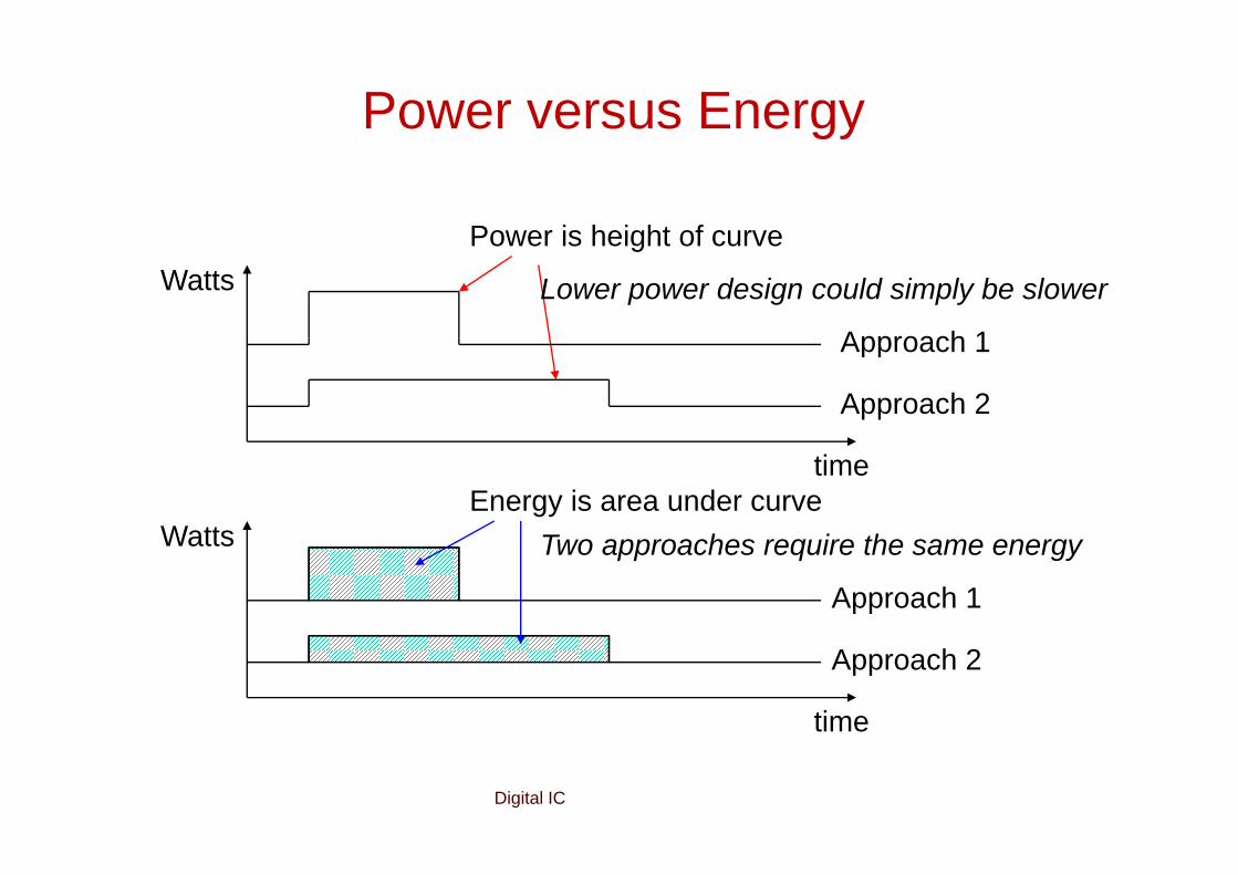
Transistor Sizing (2)g ( )• Performance Constraint (γ=1)
220
⎟⎟⎠
⎞⎜⎜⎝
⎛++
−⎟⎟⎠
⎞⎜⎜⎝
⎛++
fFf
VVVfFf
tt TErefDDpp
( ) ( ) 1330
0 =+
⎠⎝−
=+
⎠⎝=F
fVVV
VF
ftt TEDD
TEref
ref
DD
refp
p
pref
p
• Energy for single Transition
( )( )[ ]( )( )[ ]
⎞⎛⎞⎛
+++=
FfVE
FfCVE gDD
22
112
12 γ
⎟⎠⎞
⎜⎝⎛
+++
⎟⎟⎠
⎞⎜⎜⎝
⎛=
FFf
VV
EE
ref
DD
ref 422
Digital IC 17

Transistor Sizing (3)g ( )
4 1.5
VDD=f(f) E/Eref=f(f)
3
3.5
y
F=1
2
2
2.5
vdd
(V)
1
aliz
ed e
nerg
y2
5
1
1.5
v
0.5norm
a
10
20
1 2 3 4 5 6 70
0.5
f1 2 3 4 5 6 7
0
f
20
Digital IC 18

Sh t Ci it P C tiShort Circuit Power Consumption
Vin VoutIVin Vout
CL
Isc
Finite slope of the input signal causes a directFinite slope of the input signal causes a direct current path between VDD and GND for a short period of time during switching when both theperiod of time during switching when both the NMOS and PMOS transistors are conducting.
Digital IC

Short path power consumptionp p p• Direct-Path Current power consumption
Digital IC 20

Short Circuit power consumptionp p• Energy of ever switch activity
peakddfallrise
fallpeak
ddrisepeak
dddp IVtt
tI
VtI
VE222+
=+=
• Average power 222
fIVtt
P fallrise +
• Short circuit occupy no more than 20% of dynamic
fIVP peakddf
dp 2=
py ypower
Digital IC 21

An exampleAn example
• Assume rise/fall timeboth are 300ps
• Short circuit power:300ps×5V ×
0 14mA=0 21pJ0.14mA=0.21pJ• Dynamic power
30pF × 5V × 5V=0.75pJ30p 5 5 0 5pJ
Digital IC22

Short Circuit Currents DeterminatesShort Circuit Currents Determinates
E t V I PEsc = tsc VDD Ipeak P0→1
P = t V I f• Duration and slope of the input signal, tsc
I d t i d b
Psc = tsc VDD Ipeak f0→1
• Ipeak determined by • the saturation current of the P and N transistors
which depend on their sizes process technologywhich depend on their sizes, process technology, temperature, etc.
• strong function of the ratio between input and• strong function of the ratio between input and output slopes
• a function of CL
Digital IC
a function of CL

Impact of C on PImpact of CL on Psc
Vin Vout
Isc ≈ 0
Vin Vout
Isc ≈ Imax
CL CL
Large capacitive load Small capacitive loadg
O t t f ll ti i ifi tl O t t f ll ti b t ti llOutput fall time significantlylarger than input rise time.
Output fall time substantiallysmaller than the input risetime
Digital IC
time.

I as a Function of CIpeak as a Function of CL
2 5x 10⁻⁴
2
2.5
CL = 20 fF
When load capacitance is small, Ipeak is large.
1.5
0.5
1 CL = 100 fF Short circuit dissipation is minimized by
0
0.5
0 2 4 6
CL = 500 fFy
matching the rise/fall times of the input and
t t i l l-0.5
0 2 4 6
time (sec)x 10-10 output signals - slope
engineering.
Digital IC
500 psec input slope

Psc as a Function of Rise/FallPsc as a Function of Rise/Fall Times
8
6
7
8
VDD= 3.3 VWhen load capacitance is small
(tsin/tsout > 2 for VDD > 2V) the
4
5
6 DD ( sin sout DD )power is dominated by Psc
2
3
4VDD = 2.5 V If VDD < VTn + |VTp| then Psc is
eliminated since both devices are
0
1
2
VDD = 1.5Vnever on at the same time.
00 2 4tsin/tsout normalized wrt zero input rise-
time dissipationW/Lp = 1.125 μm/0.25 μm
Digital IC
pW/Lp 1.125 μm/0.25 μmW/Ln = 0.375 μm/0.25 μmCL = 30 fF
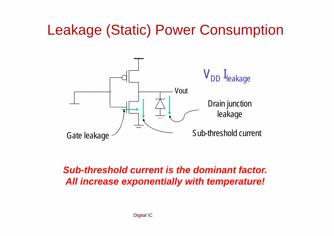
Leakage (Static) Power Consumption
VDD IleakageVoutVout
Drain junction leakageg
Sub-threshold currentGate leakage
Sub-threshold current is the dominant factorSub threshold current is the dominant factor.All increase exponentially with temperature!
Digital IC

Leakage as a Function of VLeakage as a Function of VTContinued scaling of supply voltage and the subsequent Co t ued sca g o supp y o tage a d t e subseque tscaling of threshold voltage will make subthresholdconduction a dominate component of power dissipation.
10-2 An 90mV/decade VTroll-off - so each
D (A
)10-7
255mV increase in VT gives 3 orders of magnitude reductionID
VT=0.4VVT=0.1V
magnitude reduction in leakage (but adversely affects performance)
0 0.2 0.4 0.6 0.8 1
VGS (V)
VT 0.1V
10-12performance)
Digital IC
VGS (V)

TSMC Processes Leakage and VT
1 2 V
CL013 HS
1 5 V
CL015 HS
2 V1 8 V1 8 V1 8 VVdd
CL018 HS
CL018 ULP
CL018 LP
CL018 G
0.08 μm 24 Å1.2 V
0.11 μm 29 Å1.5 V
42 Å42 Å42 Å42 ÅTox (effective)0.13 μm 0.18 μm 0.16 μm 0.16 μm Lgate
2 V1.8 V1.8 V1.8 VVdd
13 000
920/400
1 800
860/370
3000 151 6020I ff (leakage)
780/360320/130500/180600/260IDSat (n/p) (μA/μm)
0.25 V
13,000
0.29 V
1,800
0.40 V0.73 V0.63 V0.42 VVTn
3000.151.6020Ioff (leakage) (ρA/μm)
805243142230FET Perf. (GHz)
Digital ICFrom MPR, 2000

Exponential Increase in Leakage CurrentsCurrents
1000010000
1000
0.250 18A/
μm)
100 0.180.130.1I lea
kage
(n
100.1
130 40 50 60 70 80 90 100 110Temp(C) From De,1999
Digital IC
30 40 50 60 70 80 90 100 110

Principles for Power ReductionPrinciples for Power Reduction
• Prime choice: Reduce voltage!Prime choice: Reduce voltage!• Recent years have seen an acceleration in
supply voltage reductionsupply voltage reduction• Design at very low voltages still open question
(0.6 … 0.9 V by 2010!)( y )• Reduce switching activity• Reduce physical capacitancep y p
• Device Sizing: for F=20• fopt(energy)=3.53, fopt(performance)=4.47opt( gy) , opt(p )
Digital IC 31
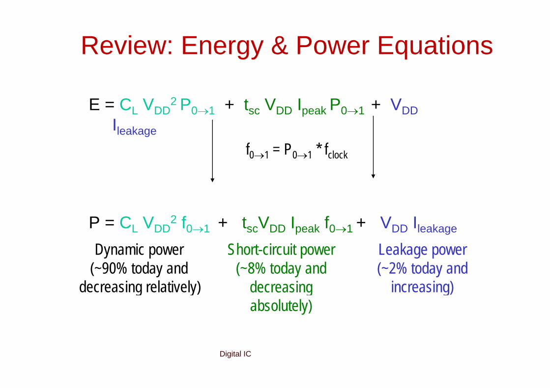
Review: Energy & Power Equations
E = C V 2 P + t V I P + VE = CL VDD P0→1 + tsc VDD Ipeak P0→1 + VDDIleakage
f = P * ff0→1 = P0→1 fclock
P = CL VDD2 f0→1 + tscVDD Ipeak f0→1 + VDD Ileakage
Dynamic power(~90% today and
d i l ti l )
Short-circuit power(~8% today and
d i
Leakage power(~2% today and
i i )decreasing relatively) decreasing absolutely)
increasing)
Digital IC

Impact ofTechnology
S liScaling
Digital ICIntroduction

Goals of Technology Scalinggy g• Make things cheaper:
• Want to sell more functions (transistors) per chip for the same money
• Build same products cheaper, sell the same part for less money
• Price of a transistor has to be reduced• But also want to be faster, smaller, lower power
Digital IC

Technology Scalinggy g• Goals of scaling the dimensions by 30%:g y
• Reduce gate delay by 30% (increase operating frequency by 43%)
• Double transistor density• Reduce energy per transition by 65% (50% power
savings @ 43% increase in frequency• Die size used to increase by 14% per y p
generation• Technology generation spans 2-3 yearsTechnology generation spans 2 3 years
Digital IC
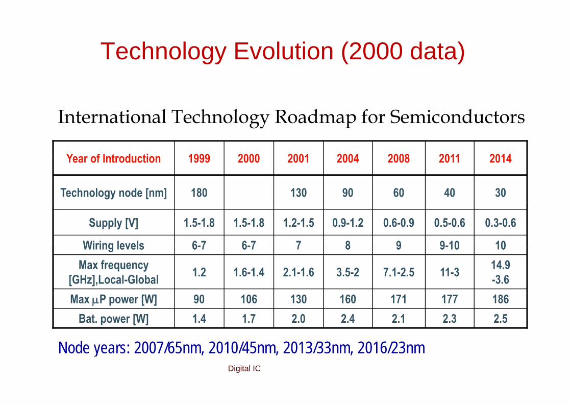
Technology Evolution (2000 data)
I i l T h l R d f S i dInternational Technology Roadmap for Semiconductors
1999 2000 20142011200820042001Year of Introd ction
180
1999 2000
30406090130Technology node [nm]
20142011200820042001Year of Introduction
6-7
1.5-1.8
6-7
1.5-1.8
109-10987Wiring levels
0.3-0.60.5-0.60.6-0.90.9-1.21.2-1.5Supply [V]
1.2
6 7
1.6-1.4
6 714.9-3.611-37.1-2.53.5-22.1-1.6Max frequency
[GHz],Local-Global
109 10987Wiring levels
18617717116013010690Max μP power [W]1.4 1.7 2.52.32.12.42.0Bat. power [W]
Digital IC
Node years: 2007/65nm, 2010/45nm, 2013/33nm, 2016/23nm

Technology Evolution (1999)Technology Evolution (1999)
Digital IC

Technology Scaling (1)gy g ( )
102
101
cro
n)
100
10re
Siz
e (
mic
-1
10
mu
m F
ea
tur
2
10
Min
im
Minimum Feature Size1960 1970 1980 1990 2000 2010
10-2
Year
Digital IC
Minimum Feature Size

Technology Scaling (2) ec o ogy Sca g ( )
Number of components per chipDigital IC
Number of components per chip

Technology Scaling (3)ec o ogy Sca g (3)
tp decreases by 13%/year50% every 5 years!50% every 5 years!
Propagation DelayPropagation DelayDigital IC
p g yp g y

Technology Scaling Models gy g• Full scaling(constant electrical)
• Ideal model –dimensions and voltage scale together by the same factor S
• Fixed voltage scaling• Most common model until recently- only dimensions
scale, voltages remain constant• General scaling
• Most realistic for today’s situation-voltages and dimensions scale with different factors
Digital IC

Scaling Relationships for Long Channel Devices g p g
Digital IC
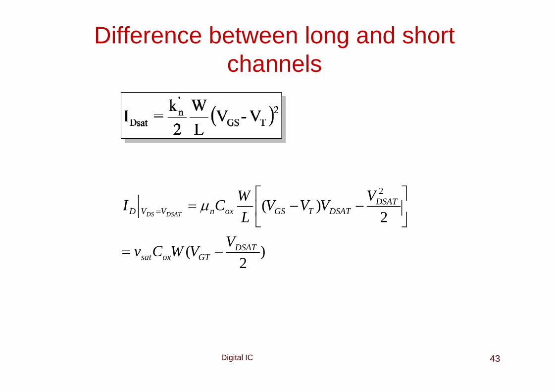
Difference between long and short channelschannels
2VW ⎤⎡2
)( DSATDSATTGSoxnVVD
V
VVVVLWCI
DSATDS ⎥⎦
⎤⎢⎣
⎡−−== μ
)2
( DSATGToxsat
VVWCv −=
Digital IC 43

Transistor Scalingg(velocity-saturated devices)
√
√√
Digital IC
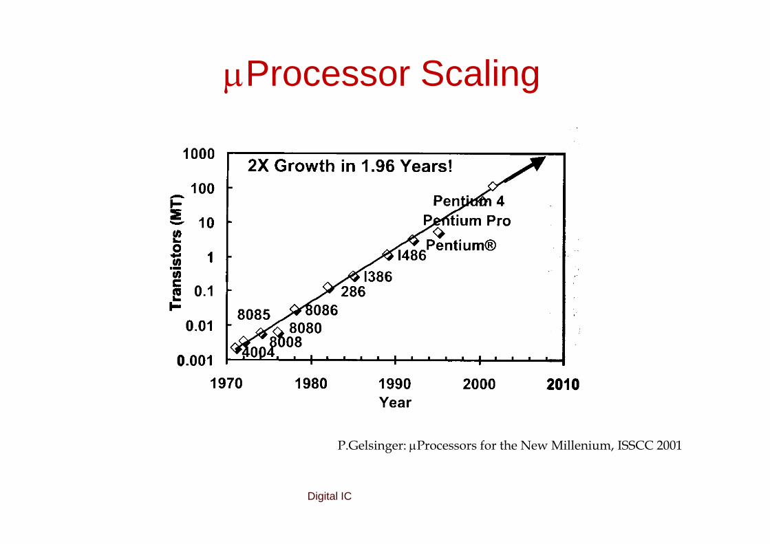
μProcessor Scalingμ g
P.Gelsinger: μProcessors for the New Millenium, ISSCC 2001
Digital IC
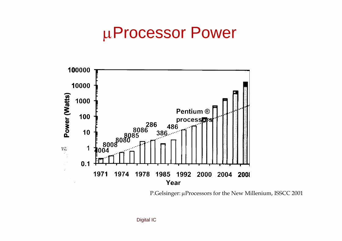
μProcessor Powerμ
P.Gelsinger: μProcessors for the New Millenium, ISSCC 2001
Digital IC
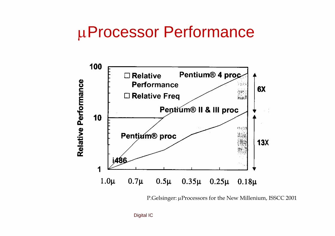
μProcessor Performanceμ
P Gelsinger: μProcessors for the New Millenium ISSCC 2001
Digital IC
P.Gelsinger: μProcessors for the New Millenium, ISSCC 2001

2010 Outlook• Performance 2X/16 months
• 1 TIP (terra instructions/s)• 30 GHz clock
• Size• No of transistors: 2 Billion• Die: 40*40 mm
• Power• 10kW!!• Leakage: 1/3 active Power
P.Gelsinger: μProcessors for the New Millenium, ISSCC 2001
Digital IC
P.Gelsinger: μProcessors for the New Millenium, ISSCC 2001
Some interesting questionsg q• What will cause this model to break?• When will it break?• Will the model gradually slow down?
• Power and power density• Leakageg• Process Variation
Digital IC

summaryy• CMOS at a glance• CMOS static behavior
• VTC, noise margin, threshold voltage• CMOS dynamic behavior
• Capacitance mosaic, delay p y• Ratio pMOS/nMOS:3.5,2.4,1.6• Optimizing inverter sizingp g g
• Power• Power mosaic• Optimizing dynamic power• Short power consideration
Digital IC
Short power consideration
50