Digital Integrated Circuitshtang/ece4311_doc_F11/LectureSlide/week… · © Digital Integrated...
58
EE141 © Digital Integrated Circuits 2nd Arithmetic Circuits 1 Digital Integrated Circuits A Design Perspective Arithmetic Circuits Jan M. Rabaey Anantha Chandrakasan Borivoje Nikolic
Transcript of Digital Integrated Circuitshtang/ece4311_doc_F11/LectureSlide/week… · © Digital Integrated...

EE141© Digital Integrated Circuits2ndArithmetic Circuits
1
Digital Integrated
CircuitsA Design Perspective
Arithmetic Circuits
Jan M. Rabaey
Anantha Chandrakasan
Borivoje Nikolic

EE141© Digital Integrated Circuits2ndArithmetic Circuits
2
A Generic Digital Processor
MEMORY
DATAPATH
CONTROL
INP
UT
-OU
TP
UT

EE141© Digital Integrated Circuits2ndArithmetic Circuits
3
Building Blocks for Digital Architectures
Arithmetic unit
- Bit-sliced datapath (adder, multiplier, shifter, comparator, etc.)
Memory
- RAM, ROM, Buffers, Shift registers
Control
- Finite state machine (PLA, random logic.)
- Counters
Interconnect
- Switches
- Arbiters
- Bus

EE141© Digital Integrated Circuits2ndArithmetic Circuits
4
Arithmetic building blocks Speed and power of arithmetic components often
dominates the overall system performance
For each module, multiple topologies and ways of
design exists, with each of them has its own advantages
A global picture is of crucial importance. A designer
focus their attention on gates or transistors that have the
largest impact on their goal function. Non-critical
components can be developed routinely.
Typically two optimization process: logic optimization
(re-arrange Boolean equations so that a faster or small
circuit could be obtained) and circuit optimization
(manipulate circuit topology and transistor sizes to
optimize speed)

EE141© Digital Integrated Circuits2ndArithmetic Circuits
5
Bit-Sliced Design
Bit 3
Bit 2
Bit 1
Bit 0
Regis
ter
Ad
der
Sh
ifte
r
Mu
ltip
lexer
Control
Data
-In
Data
-Ou
t
Tile identical processing elements
Since the same operation has to be performed on each
bit of a data word, the data path can consist of the
number of bit slices (equal to the word length), each
operating on a single bit – hence the term bit-sliced
EE141© Digital Integrated Circuits2ndArithmetic Circuits
6
Adders

EE141© Digital Integrated Circuits2ndArithmetic Circuits
7
Full-AdderA B
Cout
Sum
Cin Fulladder
Generate (G) = AB
Propagate (P) = A B
Delete (D) = A B
G,D, ensures a carry bit will be generated or deleted at Co independent of Ci,
While P guarantees that Ci will propagate to Co.

EE141© Digital Integrated Circuits2ndArithmetic Circuits
8
The Binary Adder
S A B Ci
=
A= BCi ABCi ABCi
ABCi
+ + +
Co
AB BCi
ACi
+ +=
A B
Cout
Sum
Cin Fulladder

EE141© Digital Integrated Circuits2ndArithmetic Circuits
9
The Ripple-Carry Adder
Worst case delay linear with the number of bits
Goal: Make the fastest possible carry path circuit
FA FA FA FA
A0 B0
S0
A1 B1
S1
A2 B2
S2
A3 B3
S3
Ci,0 Co,0
(= Ci,1)
Co,1 Co,2 Co,3
td = O(N)
tadder = (N-1)tcarry + tsum

EE141© Digital Integrated Circuits2ndArithmetic Circuits
10
Complimentary Static CMOS Full Adder
28 Transistors
A B
B
A
Ci
Ci A
X
VDD
VDD
A B
Ci BA
B VDD
A
B
Ci
Ci
A
B
A CiB
Co
VDD
S

EE141© Digital Integrated Circuits2ndArithmetic Circuits
11
Complimentary Static CMOS Full Adder
Large PMOS stacks are present in both carry and sum
generation circuits
Intrinsic load capacitance of Co signal is large and
consists of eight capacitance components
There is one more inverter delay for carry and sum
(worse when the load capacitance is large)
Note that critical signal Ci closer to the output node

EE141© Digital Integrated Circuits2ndArithmetic Circuits
12
Express Sum and Carry as a function of
P, G, D
Define 3 new variable which ONLY depend on A, B
Generate (G) = AB
Propagate (P) = A B
Delete (D) = A B
Can also derive expressions for S and Co based on D and P
Propagate (P) = A + B
Note that we will be sometimes using an alternate definition for

EE141© Digital Integrated Circuits2ndArithmetic Circuits
13
Transmission Gate XOR
A
B
F
B
A
B
B
M1
M2
M3/M4
tionimplementaary complementfor rs transisto12 ),( BABAF +
When B=1, M1/M2 inverter, M3/M4 off, so F=AB
When B=0, M1/M2 off, M3/M4 transmission gate, so F=AB

EE141© Digital Integrated Circuits2ndArithmetic Circuits
14
Transmission Gate Full Adder
A
B
P
Ci
VDDA
A A
VDD
Ci
A
P
AB
VDD
VDD
Ci
Ci
Co
S
Ci
P
P
P
P
P
Sum Generation
Carry Generation
SetupPropagate (P) = A B

EE141© Digital Integrated Circuits2ndArithmetic Circuits
15
Manchester Carry Chain
CoC
i
Gi
Di
Pi
Pi
VDD
CoC
i
Gi
Pi
VDD
Generate (G) = AB
Propagate (P) = A B
Delete = A B
Prevent floating Co

EE141© Digital Integrated Circuits2ndArithmetic Circuits
16
Full-AdderA B
Cout
Sum
Cin Fulladder

EE141© Digital Integrated Circuits2ndArithmetic Circuits
17
Manchester Carry Chain
G2
C3
G3
Ci,0
P0
G1
VDD
G0
P1
P2
P3
C3
C2
C1
C0

EE141© Digital Integrated Circuits2ndArithmetic Circuits
18
Manchester Carry Chain
Pi + 1
Gi + 1
Ci
Inverter/Sum Row
Propagate/Generate Row
Pi
Gi
Ci - 1
Ci + 1
VDD
GND
Stick Diagram

EE141© Digital Integrated Circuits2ndArithmetic Circuits
19
Manchester Carry Chain Delay for the Manchester Carry Chain can be
modeled similar to a linearized RC network as in
transmission-gates
This means the propagation delay is quadratic in the
number of bits N (but does not imply the delay will be
larger than the ripple carry adder)
It might be necessary to insert signal buffering
inverters.
Still a ripple carry adder, typically only good for small
word length (<8/16 bits)
We need faster adders for computer and multimedia
applications with word length 32-128 bits

EE141© Digital Integrated Circuits2ndArithmetic Circuits
20
Carry-Bypass Adder
FA FA FA FA
P0 G1 P0 G1 P2 G2 P3 G3
Co,3Co,2Co,1Co,0Ci ,0
FA FA FA FA
P0 G1 P0 G1 P2 G2 P3 G3
Co,2Co,1Co,0Ci,0
Co,3
Mu
ltip
lexer
BP=PoP1P2P3
Idea: If (P0 and P1 and P2 and P3 = 1)
then Co3 = C0, else “kill” or “generate”.
Also called
Carry-Skip
Break the bit-slice organization
G0
G0
P1
P1
“delete” or “generate”

EE141© Digital Integrated Circuits2ndArithmetic Circuits
21
Carry-Bypass Adder (cont.)
Carrypropagation
Setup
Bit 0–3
Sum
M bits
tsetup
tsum
Carrypropagation
Setup
Bit 4–7
Sum
tbypass
Carrypropagation
Setup
Bit 8–11
Sum
Carrypropagation
Setup
Bit 12–15
Sum
tadder = tsetup + Mtcarry + (N/M-1)tbypass + (M-1)tcarry + tsum
Tsetup: overhead time to create G, P, D signals
(worst case)

EE141© Digital Integrated Circuits2ndArithmetic Circuits
22
Carry Ripple versus Carry Bypass
(both still linear)
N
tp
ripple adder
bypass adder
4..8

EE141© Digital Integrated Circuits2ndArithmetic Circuits
23
Carry-Select Adder
Setup
"0" Carry Propagation
"1" Carry Propagation
Multiplexer
Sum Generation
Co,k-1 Co,k+3
"0"
"1"
P,G
Carry Vector

EE141© Digital Integrated Circuits2ndArithmetic Circuits
24
Carry Select Adder: Critical Path
0
1
Sum Generation
Multiplexer
1-Carry
0-Carry
Setup
Ci,0 Co,3 Co,7 Co,11 Co,15
S0–3
Bit 0–3 Bit 4–7 Bit 8–11 Bit 12–15
0
1
Sum Generation
Multiplexer
1-Carry
0-Carry
Setup
S4–7
0
1
Sum Generation
Multiplexer
1-Carry
0-Carry 0-Carry
Setup
S8–11
0
1
Sum Generation
Multiplexer
1-Carry
Setup
S12–15

EE141© Digital Integrated Circuits2ndArithmetic Circuits
25
Linear Carry Select
Setup
"0" Carry
"1" Carry
Multiplexer
Sum Generation
"0"
"1"
Setup
"0" Carry
"1" Carry
Multiplexer
Sum Generation
"0"
"1"
Setup
"0" Carry
"1" Carry
Multiplexer
Sum Generation
"0"
"1"
Setup
"0" Carry
"1" Carry
Multiplexer
Sum Generation
"0"
"1"
Bit 0-3 Bit 4-7 Bit 8-11 Bit 12-15
S0-3 S4-7 S8-11 S12-15
Ci,0
(1)
(1)
(5)(6) (7) (8)
(9)
(10)
(5) (5) (5)(5)
tadder = tsetup + Mtcarry + (N/M)tmux + tsum

EE141© Digital Integrated Circuits2ndArithmetic Circuits
26
Square Root Carry Select
Setup
"0" Carry
"1" Carry
Multiplexer
Sum Generation
"0"
"1"
Setup
"0" Carry
"1" Carry
Multiplexer
Sum Generation
"0"
"1"
Setup
"0" Carry
"1" Carry
Multiplexer
Sum Generation
"0"
"1"
Setup
"0" Carry
"1" Carry
Multiplexer
Sum Generation
"0"
"1"
Bit 0-1 Bit 2-4 Bit 5-8 Bit 9-13
S0-1 S2-4 S5-8 S9-13
Ci,0
(4) (5) (6) (7)
(1)
(1)
(3) (4) (5) (6)
Mux
Sum
S14-19
(7)
(8)
Bit 14-19
(9)
(3)
M

EE141© Digital Integrated Circuits2ndArithmetic Circuits
27
Adder Delays - Comparison
Square root select
Linear select
Ripple adder
20 40
N
t p(in
un
it d
ela
ys)
600
10
0
20
30
40
50
Bypass

EE141© Digital Integrated Circuits2ndArithmetic Circuits
28
LookAhead - Basic Idea
Co k f Ak Bk Co k 1– Gk PkCo k 1–+= =
AN-1, BN-1A1, B1
P1
S1
• • •
• • • SN-1
PN-1Ci, N-1
S0
P0Ci,0 Ci,1
A0, B0

EE141© Digital Integrated Circuits2ndArithmetic Circuits
29
Look-Ahead: Topology
Co k Gk Pk Gk 1– Pk 1– Co k 2–+ +=
Co k Gk Pk Gk 1– Pk 1– P1 G0 P0Ci 0+ + + +=
Expanding Lookahead equations:
All the way:
Co,3
Ci,0
VDD
P0
P1
P2
P3
G0
G1
G2
G3

EE141© Digital Integrated Circuits2ndArithmetic Circuits
30
Look-Ahead Adder: Logarithmic adder
A7
F
A6A5A4A3A2A1
A0
A0
A1
A2
A3
A4
A5
A6
A7
F
tp log2(N)
tp N

EE141© Digital Integrated Circuits2ndArithmetic Circuits
31
Carry Look-Ahead Trees
Can continue building the tree hierarchically.
=G1:0+P1:0C0
(G1:0=G1+P1G0 P1:0=P1P0)
C0=G0+P0Cin
C1=G1+P1C0
C2=G2+P2C1
C3=G3+P3C2
C0=G0+P0Cin
C1=G1+P1C0 =G1+G0P1+P1P0Cin
C2=G2+P2C1 =G2+G1P2+G0P2P1+P2P1P0Cin =G2:1+P2:1C0
(G2:1=G2+P2G1 P2:1=P2P1)
C3=G3+P3C2 =G3+G2P3+G1P3P2+G0P3P2P1+P3P2P1P0Cin
=G3:2+P3:2C1=G3:2+P3:2(G1:0+P1:0C0)=(G3:2+P3:2G1:0)+P3:2P1:0C0
G3:2=(G3+P3G2) and P3:2=P3P2 are called dot products.

EE141© Digital Integrated Circuits2ndArithmetic Circuits
32
Tree Adders
16-bit radix-2 Kogge-Stone tree (radix 2 means that the tree is
Binary: it combines two dot product or carry words at a time at
Each level of hierarchy)
(A0,
B0)
(A1,
B1)
(A2,
B2)
(A3,
B3)
(A4,
B4)
(A5,
B5)
(A6,
B6)
(A7,
B7)
(A8,
B8)
(A9,
B9)
(A10,
B10)
(A11,
B11)
(A12,
B12)
(A13,
B13)
(A14,
B14)
(A15,
B15)
S0
S1
S2
S3
S4
S5
S6
S7
S8
S9
S10
S11
S12
S13
S14
S15

EE141© Digital Integrated Circuits2ndArithmetic Circuits
33
Tree Adders(a
0,
b0)
(a1,
b1)
(a2,
b2)
(a3,
b3)
(a4,
b4)
(a5,
b5)
(a6,
b6)
(a7,
b7)
(a8,
b8)
(a9,
b9)
(a1
0,
b1
0)
(a1
1,
b1
1)
(a1
2,
b1
2)
(a1
3,
b1
3)
(a1
4,
b1
4)
(a1
5,
b1
5)
S0
S1
S2
S3
S4
S5
S6
S7
S8
S9
S1
0
S1
1
S1
2
S1
3
S1
4
S1
5
16-bit radix-4 Kogge-Stone Tree

EE141© Digital Integrated Circuits2ndArithmetic Circuits
34
Sparse Trees(a
0,
b0)
(a1,
b1)
(a2,
b2)
(a3,
b3)
(a4,
b4)
(a5,
b5)
(a6,
b6)
(a7,
b7)
(a8,
b8)
(a9,
b9)
(a1
0,
b1
0)
(a1
1,
b1
1)
(a1
2,
b1
2)
(a1
3,
b1
3)
(a1
4,
b1
4)
(a1
5,
b1
5)
S1
S3
S5
S7
S9
S1
1
S1
3
S1
5
S0
S2
S4
S6
S8
S1
0
S1
2
S1
4
16-bit radix-2 sparse tree with sparseness of 2

EE141© Digital Integrated Circuits2ndArithmetic Circuits
35
Tree Adders(A
0,
B0)
(A1,
B1)
(A2,
B2)
(A3,
B3)
(A4,
B4)
(A5,
B5)
(A6,
B6)
(A7,
B7)
(A8,
B8)
(A9,
B9)
(A1
0,
B1
0)
(A1
1,
B1
1)
(A1
2,
B1
2)
(A1
3,
B1
3)
(A1
4,
B1
4)
(A1
5,
B1
5)
S0
S1
S2
S3
S4
S5
S6
S7
S8
S9
S1
0
S1
1
S1
2
S1
3
S1
4
S1
5
Brent-Kung Tree

EE141© Digital Integrated Circuits2ndArithmetic Circuits
36
Intel Itanium Microprocessor
9-1
Mu
x9
-1 M
ux
5-1
Mu
x2
-1 M
ux
ck1
CARRYGEN
SUMGEN
+ LU
1000um
b
s0
s1
g64
sum sumb
LU : Logical
Unit
SU
MS
EL
a
to Cache
node1
RE
GItanium has 6 integer execution units like this

EE141© Digital Integrated Circuits2ndArithmetic Circuits
37
Bit-Sliced Design
Bit 3
Bit 2
Bit 1
Bit 0
Regis
ter
Ad
der
Sh
ifte
r
Mu
ltip
lexer
Control
Data
-In
Data
-Ou
t
Tile identical processing elements

EE141© Digital Integrated Circuits2ndArithmetic Circuits
38
Bit-Sliced Datapath
Adder stage 1
Wiring
Adder stage 2
Wiring
Adder stage 3
Bit s
lice
0
Bit s
lice
2
Bit s
lice
1
Bit s
lice
63
Sum Select
Shifter
Multiplexers
Loopback B
us
From register files / Cache / Bypass
To register files / Cache
Loopback B
us
Loopback B
us
The adder is
implemented
as a radix-4
Carry Look-
Ahead adder,
the red lines
are forwarding
the results of
different stages

EE141© Digital Integrated Circuits2ndArithmetic Circuits
39
Itanium Integer Datapath
Courtesy of Intel

EE141© Digital Integrated Circuits2ndArithmetic Circuits
40
Multipliers

EE141© Digital Integrated Circuits2ndArithmetic Circuits
41
The Binary Multiplication
Z X··
Y Zk2k
k 0=
M N 1–+
= =
Xi2i
i 0=
M 1–
Yj2j
j 0=
N 1–
=
XiYj2i j+
j 0=
N 1–
i 0=
M 1–
=
X Xi2i
i 0=
M 1–
=
Y Yj2j
j 0=
N 1–
=
with

EE141© Digital Integrated Circuits2ndArithmetic Circuits
42
The Binary Multiplication
x
+
Partial products
Multiplicand
Multiplier
Result
1 0 1 0 1 0
1 0 1 0 1 0
1 0 1 0 1 0
1 1 1 0 0 1 1 1 0
0 0 0 0 0 0
1 0 1 0 1 0
1 0 1 1

EE141© Digital Integrated Circuits2ndArithmetic Circuits
43
The Array Multiplier (4 by 4)
Y0
Y1
X3 X2 X1 X0
X3
HA
X2
FA
X1
FA
X0
HA
Y2X3
FA
X2
FA
X1
FA
X0
HA
Z1
Z3Z6Z7 Z5 Z4
Y3X3
FA
X2
FA
X1
FA
X0
HA
Z2
Z0
The carryout of the last adder for Yi is forwarded to Yi+1
carry
sum
Half
adder

EE141© Digital Integrated Circuits2ndArithmetic Circuits
44
The MxN Array Multiplier
— Critical Path
HA FA FA HA
HAFAFAFA
FAFA FA HA
Critical Path 1
Critical Path 2
Critical Path 1 & 2
EE141© Digital Integrated Circuits2ndArithmetic Circuits
45
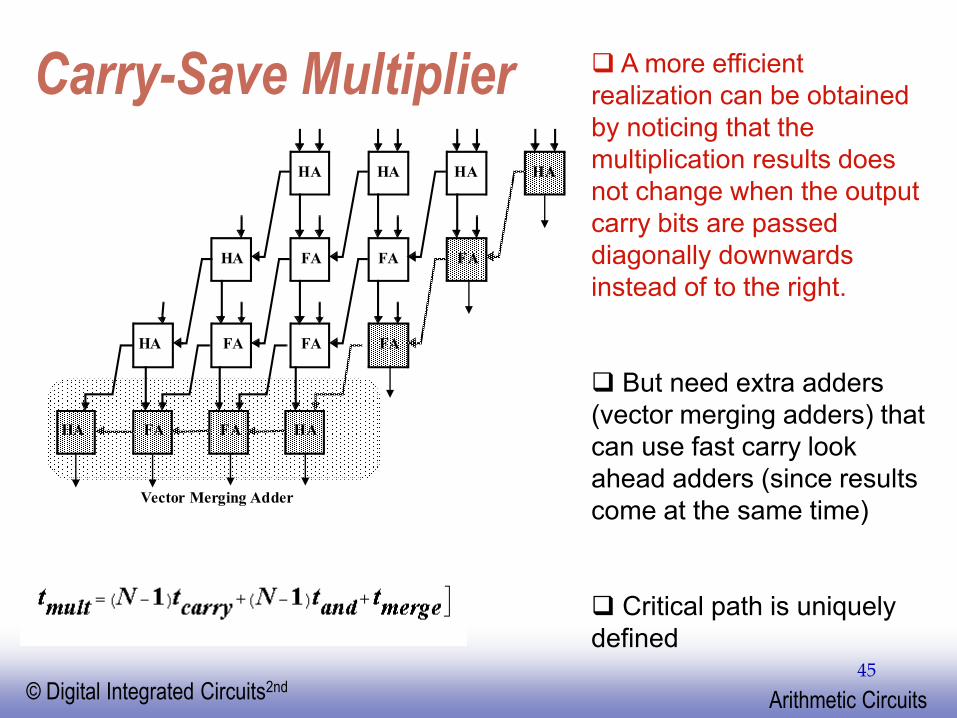
Carry-Save Multiplier
HA HA HA HA
FAFAFAHA
FAHA FA FA
FAHA FA HA
Vector Merging Adder
A more efficient
realization can be obtained
by noticing that the
multiplication results does
not change when the output
carry bits are passed
diagonally downwards
instead of to the right.
But need extra adders
(vector merging adders) that
can use fast carry look
ahead adders (since results
come at the same time)
Critical path is uniquely
defined

EE141© Digital Integrated Circuits2ndArithmetic Circuits
46
Multiplier Floorplan
SCSCSCSC
SCSCSCSC
SCSCSCSC
SC
SC
SC
SC
Z0
Z1
Z2
Z3Z4Z5Z6Z7
X0X1X2X3
Y1
Y2
Y3
Y0
Vector Merging Cell
HA Multiplier Cell
FA Multiplier Cell
X and Y signals are broadcasted
through the complete array.
( )

EE141© Digital Integrated Circuits2ndArithmetic Circuits
47
Wallace-Tree Multiplier
6 5 4 3 2 1 0 6 5 4 3 2 1 0
Partial products First stage
Bit position
6 5 4 3 2 1 0 6 5 4 3 2 1 0
Second stage Final adder
FA HA
(a) (b)
(c) (d)
Save the number of full adders
Increase the complexity of routing

EE141© Digital Integrated Circuits2ndArithmetic Circuits
48
Wallace-Tree Multiplier
HA
Can use carry Look-Ahead adder for the last stage

EE141© Digital Integrated Circuits2ndArithmetic Circuits
49
Wallace-Tree Multiplier
FA
FA
FA
FA
y0 y1 y2
y3
y4
y5
S
Ci-1
Ci-1
Ci-1
Ci
Ci
Ci
FA
y0 y1 y2
FA
y3 y4 y5
FA
FA
CC S
Ci-1
Ci-1
Ci-1
Ci
Ci
Ci

EE141© Digital Integrated Circuits2ndArithmetic Circuits
50
Booth encoding Multiply by 01111110 gives 8 partial products, but two
are all zero. Add these zero is waste of time.
Instead, multiply by 100000010, where 1 stands for -1.
Then you need to only add (actually subtract) partial
products, which improves speed
This kind of transformation is called booth encoding. It
reduces the number of partial product to at most half of
the original multiplier width.
The encoding logic is easily incorporated in the overall
multiplier design.
EE141© Digital Integrated Circuits2ndArithmetic Circuits
51
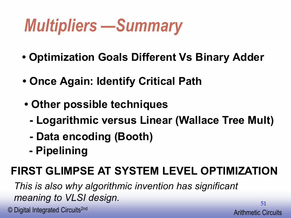
Multipliers —Summary
• Optimization Goals Different Vs Binary Adder
• Once Again: Identify Critical Path
• Other possible techniques
- Data encoding (Booth)
- Pipelining
FIRST GLIMPSE AT SYSTEM LEVEL OPTIMIZATION
- Logarithmic versus Linear (Wallace Tree Mult)
This is also why algorithmic invention has significant
meaning to VLSI design.

EE141© Digital Integrated Circuits2ndArithmetic Circuits
52
Shifters

EE141© Digital Integrated Circuits2ndArithmetic Circuits
53
The Binary Shifter
Ai
Ai-1
Bi
Bi-1
Right Leftnop
Bit-Slice i
...

EE141© Digital Integrated Circuits2ndArithmetic Circuits
54
The Barrel Shifter
Sh3Sh2Sh1Sh0
Sh3
Sh2
Sh1
A3
A2
A1
A0
B3
B2
B1
B0
: Control Wire
: Data Wire
Area Dominated by Wiring
Column: maximum shift
Word length

EE141© Digital Integrated Circuits2ndArithmetic Circuits
55
4x4 barrel shifter
BufferSh3Sh2Sh1Sh0
A3
A2
A1
A0
Coder/decoder required to set shift bits
Signal pass through one gate independent of shift
amount (parasitic capacitance may change the picture)

EE141© Digital Integrated Circuits2ndArithmetic Circuits
56
Logarithmic ShifterSh1 Sh1 Sh2 Sh2 Sh4 Sh4
A3
A2
A1
A0
B1
B0
B2
B3
No separate coder/decoder is required

EE141© Digital Integrated Circuits2ndArithmetic Circuits
57
A3
A2
A1
A0
Out3
Out2
Out1
Out0
0-7 bit Logarithmic Shifter
Good for large shift amount (note that cascade pass
transistor slow down the gate and generate weak signals,
buffers may be needed)

EE141© Digital Integrated Circuits2ndArithmetic Circuits
58
Building Blocks for Digital Architectures
Arithmetic unit
- Bit-sliced datapath (adder, multiplier, shifter, comparator)
(comparator, divider, sin, cos etc)