Digital Integrated Circuit Design I ECE 425/525 …web.cecs.pdx.edu/~ecex25/pdf/chapter9.pdfDigital...
29
Digital Integrated Circuit Design I ECE 425/525 Chapter 9 Professor R. Daasch Department of Electrical and Computer Engineering Portland State University Portland, OR 97207-0751 ([email protected]) http://ece.pdx.edu/~ecex25 ©R.Daasch, Portland State University 1 December 2014
Transcript of Digital Integrated Circuit Design I ECE 425/525 …web.cecs.pdx.edu/~ecex25/pdf/chapter9.pdfDigital...

Digital Integrated Circuit Design IECE 425/525
Chapter 9
Professor R. Daasch
Depar tment of Electrical and Computer EngineeringPortland State UniversityPortland, OR 97207-0751([email protected])
http://ece .pdx.edu/ ~ecex25
©R.Daasch, Por tland State University 1 December 2014

Chapter 9Chapter 9 demonstrates a difference in sizing the transistorsfor different logic gate designs
Static CMOS
Ratioed circuits and
Dynamic circuits
Each may have new base inverter changes the pull-up andpulldown sizing
Delay is propor tional to three quantities
t ∝ C∆VI
Simple static gate design (Chapter 1 and Chapter 4) aremodified to improve perfor mance
Input order changes the delays
©R.Daasch, Por tland State University 2 December 2014

Chapter 9Different sizing in transistor stack
Modified to yield many new logic families
Multiple threshold voltage or different NFET/PFETthresholds
Skew the unit current for pullup and pulldown
Gang gates input combinations yield ratio and static gate
Dynamic logic reduce delay by design circuit with smaller totalswitching capacitance C
Dynamic logic uses NFETs only for generally larger I
The rail-to-rail ∆V = VDD is unchanged
Differential schemes using sense amplifiers reduce delay byreducing the voltage swing ∆V of the logic transition
Increased I is possible by logic function in NFET onlytopology
©R.Daasch, Por tland State University 3 December 2014

Chapter 9Dual rail replaces single rail for not much change in C
Skew ed gates reduce the ∆V required for a selected transition
Sizing is based per transition
Tw o reference inverters to track
Unlike other examples (ie dynamic, CVSL) reducedcurrents increase delay
Chapter 9 also introduces dynamic logic circuits the secondmajor class of combinational and sequential circuits.
©R.Daasch, Por tland State University 4 December 2014

Chapter 9
Digital Circuits
Clocked=No Clocked=Yes
Dynamic Circuits
Rail=1 Rail=2
Static Circuits
Rail=1 Rail=2
CVSL CMOS Classical CMOS Domino Logic SSD Logic
Dynamic circuits can provide perfor mance advantages at thecost of complexity in analysis and design
Although more complex to design, typically less siliconarea
High-perfor mance designs utilize dynamic circuits (typically astyle called domino) in circuitry that has the largest delay
©R.Daasch, Por tland State University 5 December 2014

Chapter 9called the critical path
Each advantage can quickly become a disadvantage
C load reduced from lower transistor count
The clock node has considerably more capacitance that alogic node
Basic principle of dynamic circuits is charge storage onintr insic capacitance of a MOS circuit
Updating (restoring) is required as charge storage of alogic value has limited lifetime
Domino logic is attractive for high-speed circuits
1.3 — 2x faster than static CMOS
Monotonicity, leakage, charge sharing, noise
More popular in high-perfor mance microprocessors in 90’s
©R.Daasch, Por tland State University 6 December 2014

Chapter 9Largely displaced by static CMOS now that power is thelimiter
Still used in memories for area efficiency
The soft-node is a MOS circuit drain node isolated from thenFET (pFET) branch to GND (VDD )
Domino soft-node is common drain at PFET prechargeand top of NFET pulldown stack
Need new values for g and p and must account for the extraoutput inverter
d = g ⋅ h + p
becomes
d = g in ⋅ gHI ⋅ h + p
where gHI is the HI-skew inver ter
©R.Daasch, Por tland State University 7 December 2014

Chapter 9Isolating a capacitive node means increased sensitivity tonoise
Capacitive coupling between passive/active nodes logic(circuit) nodes are an example of a victim, aggressor pair
Resistive coupling between two passive nodes (chargeshar ing)
Intr insic leakage (p-n junction + Isubthres )
Capacitor voltage (Vdd and GND) are two logic states
Isolated capacitor is the simplest (and potentially mostunreliable) logic storage element
Remember any MOS circuit node sum of several parallellinear and nonlinear capacitors
C load = Cgd ,n + Cgd ,p + Cdb,n + Cdb,p + C int
©R.Daasch, Por tland State University 8 December 2014

Chapter 9Only a small part is parasitic capacitance (ie unwanted butunavoidable and sets minimum gate delay)
The effects of leakage currents are accumulated over time
Static logic circuits provide a “replacement” mechanism forthe charge leaked (lost)
• Subthreshold leakage is increasing with technologyscaling
• Gate current (transistors controlled by soft-node)histor ically ignored
• Deep-submicron thin-oxide are scaled (reduced) topoint where gate leakage is growing concern fordynamic circuits
• Source/Drain leakage from reverse bias of junction andgeneration (thermal and radiation)
©R.Daasch, Por tland State University 9 December 2014

Chapter 9Typical time constants are in 1-100 ms
Tr aditionally dynamic circuits offered lower pow er than static
At deep-submicron the power savings is diminished andmany cases worse
Domino gates have high activity factors
Output evaluates and precharges
Output probability P = 0. 5, α = 0. 5
Output rises and falls on half the cycles
Clocked transistors have α = 1
Leads to ver y high power consumption
Pdynamic = C loadV 2DDf
Synchronization is explicit as each gate has a clock input
©R.Daasch, Por tland State University 10 December 2014
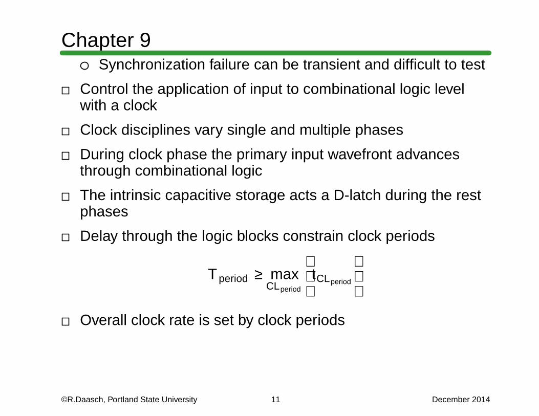
Chapter 9Synchronization failure can be transient and difficult to test
Control the application of input to combinational logic levelwith a clock
Clock disciplines var y single and multiple phases
Dur ing clock phase the primar y input wavefront advancesthrough combinational logic
The intrinsic capacitive storage acts a D-latch during the restphases
Delay through the logic blocks constrain clock per iods
Tperiod ≥CLperiod
maxtCLperiod
Overall clock rate is set by clock per iods
©R.Daasch, Por tland State University 11 December 2014

Chapter 9
T≥ maxTperiod
Control the evaluation of the input of a combination logic levelwith a clock
Inputs are not explicitly gated
Input effect on the output is gated in the load, driver orboth
Precharge phase when the load of the combination logic levelis gated on
Evaluation phase when the driver of the combination logiclevel is gated on
Each output then is in one of two distinct conditionsdepending on the clock phase
©R.Daasch, Por tland State University 12 December 2014

Chapter 9Dur ing precharge the output is unconditionally set to a logichigh or logic low
Precharge can be thought of as guessing the output
Dur ing ev aluation the output assumes the correct final valuebased on the input and the combinational logic (fix the guess)
Evaluate can be thought of as correcting for the cases theguess is incorrect
If the precharge value is generally wrong power consumptionis worse than static logic
P = αC loadV 2DDf
α is larger in the dynamic logic case
The stored charge of the precharge phase has to be carefullyused
If the delays cause a premature “fix” of the output norestor ing circuit can recover the lost charge
©R.Daasch, Por tland State University 13 December 2014

Chapter 9The synchronization failure is propagated downstream forunknown number of clock cycles
Recovery is difficult and unreliable
Domino Circuits
Non-inverting logic (AND, OR) only
Most common dynamic logic implementation
In general dynamic circuits have two distinct states
• The guess or precharge value is obtained with as few asa single transistor
• The correction is a networ k of one or more transistors inser ies and parallel that determine the logic function
The (required) inversion must be at a register input oroutput to domino logic block
©R.Daasch, Por tland State University 14 December 2014

Chapter 9Eliminates the race condition from simple dynamic logicschemes
Domino logic is a preferred for reducing delay
Reduced input capacitance
Output transitions begin sooner (no switching current)
Cascade logic is simple to divide for equal delay
Domino logic has additional composition rules
Domino logic blocks may be as small as a single gate perclock (precharge/evaluate) pair
No active path from output to alternate rail duringprecharge cycle
Each dynamic (domino) gates are separated by a staticgate (typically an inverter)
©R.Daasch, Por tland State University 15 December 2014

Chapter 9Clocked buffers typically terminate a domino combinationallogic block
Input transitions are monotonic
• High to low for p-FET inputs
• Low to high for n-FET inputs
Clock skew is a key concer n for domino circuits
What is clock skew?
Much more next term in Chapter 10
For the most part the clock signals are global and delaypaths from driver to receiver differ
Ideally signaling a dynamic circuit to switch from prechargeto evaluate is simultaneous across chip
Different finite in the clock lines blurs the transition
©R.Daasch, Por tland State University 16 December 2014

Chapter 9Clock skew that exceeds the (precharge/evaluate) dutycycle causes delay fails that appear as transient logic fails
Many domino logic block implementations use both CMOStransistors, nFET and pFET
Alter nating nFET/pFET logic blocks eliminate the explicitinverter
NP CMOS — alternatives noise problems from (downstream)inputs driven not by static inverter but the soft-node
Domino logic is a high-perfor mance logic family transistorplacement and sizing are key
Reduce the input capacitance as much as possible
Predict input signal delays to optimize transistor order
Charge sharing of internal (an likely not precharged)capacitance can erode output signal
©R.Daasch, Por tland State University 17 December 2014

Chapter 9• Helps to have large load capacitance CY common drain
• Note not the output
Output buffers can be modified to provide a weak staticoutput (keepers)
• A single feedback transistor provides a small current to“hold” the output to the precharged logic value duringev aluation
• Transistor is weak (ie drawn long) to limit the unavoidableaddition of a switching current
• Secondar y precharge transistors
• Precharge every other internal node
Domino gates can have multiple outputs
• Each precharged node can be a separate output
©R.Daasch, Por tland State University 18 December 2014

Chapter 9• Precharging internal nodes also reduces the charge
shar ing problem
• Each output has to have a dedicated buffer (againtypically an inverter)
Dynamic circuits are not robust to noise but all circuits fail
• diode drops, ratio logic, leakage, charge sharing, signal-signal or input-output coupling, race conditions
• Leakage, signal coupling, soft errors (radiation) andcharge sharing are a primar y concer n for prechargenodes
• Low noise margin process corner is when prechargetransistors are weak FS (PFET pullup precharge) or SF(NFET pulldown pre-discharge)
Bootstrapping (capacitive coupling 101)
©R.Daasch, Por tland State University 19 December 2014

Chapter 9The basic idea is to generate a voltage at the gate terminalof a n(p)-FET to a voltage above (below) the supply(ground) rail
The term comes from the phase “pull oneself up by one’sbootstraps”
AC coupling is (bootstrapped given a bad name) causesmany failures such as back-gate
Bootstrapped circuits are also attractive
An increased drive current results from the VGS −VTincrease (over-dr ive)
Increased VGS also means that the VT losses from n-FETsin pullup or p-FETs in pulldown can be recovered
Reduce static power for ratio design techniques
Situations where these conditions are present include
©R.Daasch, Por tland State University 20 December 2014

Chapter 9Pseudo-nmos circuits where VOL is too high
Long bus lines (large capacitive load) requiring larger drivecurrents
Pass transistor logic — simplest (lowest transistor count) logicfamilies
Based on simple multiplexer logic design
Voltage/current steering replaces conventional logicfunction
Input is routed to output by low-resistance path
Pass transistor or transmission gates (TG) in the signal path
nFET pass transistor logic can reduce logic swing fromGND — VDD to GND — VDD −VT ,n
pFET pass transistor logic can reduce logic swing fromGND — VDD to |VT ,p | — VDD
©R.Daasch, Por tland State University 21 December 2014

Chapter 9TG can gate load (eg dynamic inputs), gate driver (egclock control) or both
TG and pass transistor perfor mance claims var y
Str ict area requirements may benefit special area circuitrysuch as a memory
TG areas for XOR/XNOR is particular ly reduced (simplenetwor k and easy to complement)
Partial inventor y of TG and pass transistor logic
CPL (Complementary Pass transistor Logic) modifiedCascode Voltage Switch Logic a differential scheme
LEAP (Lean Integration Pass Transistors) modifiesmultiplexer to NFET only and the modularity problems oflow signal swing
DPL (Double Rail Pass Transistor) uses TG on a LEAPmultiplexer
©R.Daasch, Por tland State University 22 December 2014

Chapter 9Caution is called for with bootstrapped circuits (CMOS inpar ticular)
The latch-up condition can be triggered; locking up ordestroying the circuit
Bootstrapped circuits are intentional capacitive couplingreducing noise immunity
Supply bounce can nullify many bootstrapped techniques
Premature or otherwise unintentional bootstrap action(really the noise immunity problem again)
The relationship of three capacitors is the key to bootstrapmethods
Cout — output capacitance to ground (the load),Cs — storage (floating) node capacitance to ground,Cboot — boot to output capacitance
©R.Daasch, Por tland State University 23 December 2014

Chapter 9Cboot is the AC coupling capacitors that permits bootstrapping
Commonly a FET wired as a capacitor
Storage node and output intrinsic capacitance enough
Rarely a simple two-plate capacitor
©R.Daasch, Por tland State University 24 December 2014

Chapter 9The diode connected transistor is one-way (ie assume nocharge can leak back into supply)
Simple charge calculations based on the voltages across thethree capacitors describes the bootstrapping action
Cboot =2VT
(VDD − 2VT −VOL)Cs
Larger Cs requires a larger Cboot
Smaller VT and VOL requires smaller Cboot
Ratio circuits
Ratio logic replaces the precharge transistor with a fixedload
No change in the logic (gates remain inverting NAND,NOR...)
©R.Daasch, Por tland State University 25 December 2014

Chapter 9Similar ly reduces the capacitance on the active input(nFET only)
pFET to nFET limited by VOL not delay
Delays have own normalization currents
Pullup and pulldown not complementary and interact indelay calculation
Net Pulldown Current = Ipulldown − Ipullup
=43
I −13
I
Inter nal delays are also unique parasitics (similar argumentas HI-skew, LO-skew etc.)
Current mirrors provide circuit lever for process tracking
Other logic families and distinguishing character istics
©R.Daasch, Por tland State University 26 December 2014
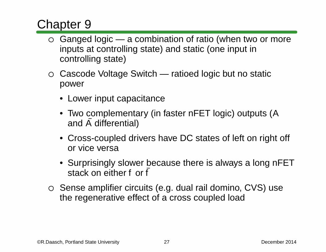
Chapter 9Ganged logic — a combination of ratio (when two or moreinputs at controlling state) and static (one input incontrolling state)
Cascode Voltage Switch — ratioed logic but no staticpower
• Low er input capacitance
• Two complementar y (in faster nFET logic) outputs (Aand A differential)
• Cross-coupled drivers have DC states of left on right offor vice versa
• Sur prisingly slower because there is always a long nFETstack on either f or f
Sense amplifier circuits (e.g. dual rail domino, CVS) usethe regenerative effect of a cross coupled load
©R.Daasch, Por tland State University 27 December 2014

Chapter 9Both voltage (common) and current sense amplifiers
Combinational logic problems
Threshold drops — pass transistor logic
Ratio failures — strong pFET forces a larger VOL
Leakage — dynamic node drops(rises) into forbidden logicrange
Charge sharing — device capacitance is everywhere(between every transistor
Po wer supply noise — soft-nodes and delay effects
Coupling — soft-nodes again aggressor node resets asoft-node
Hot spots — all transistors are not alike and all regions onthe device are not the same temperature
©R.Daasch, Por tland State University 28 December 2014

Chapter 9Back gating — downstream logic forcing the value of aupstream soft (dynamic) node
Minor ity Carr ier — substrates collect the charge fromcapacitive or inductive coupling to active signals
©R.Daasch, Por tland State University 29 December 2014