
Digital Electronics Assignment: Date of Birth...
25
1 Digital Electronics Assignment: Date of Birth Circuit Your goal is to design a circuit that will control the segments of a common cathode 7 segment display. The display will sequence through the month, day and year (2 digit) of your birthday. Below is a table of contents for this document. Topic Author Pages Project Overview mr. Hanley 2 Project Overview/CheckList mr. Hanley 3 Intro to PLDS PLTW dude person 5-6 A Basic PLD Problem PLTW dude person 7-12 Date of Birth Description PLTW dude person 19-20 Hanley Date of Birth Circuit mr. Hanley 21 7 segment display datasheet Quality Technologies 22 Pinout for 74163 Counter mr. Hanley 21 Hand drawn diagram for 74163 Counter mr. Hanley 22 Writing up a report mr. Hanley 23 Project Rubric mr. Hanley 24
Transcript of Digital Electronics Assignment: Date of Birth...

1
Digital Electronics Assignment: Date of Birth Circuit
Your goal is to design a circuit that will control the segments of a common cathode 7 segment display. The
display will sequence through the month, day and year (2 digit) of your birthday.
Below is a table of contents for this document.
Topic Author Pages Project Overview mr. Hanley 2
Project Overview/CheckList mr. Hanley 3
Intro to PLDS PLTW dude person 5-6
A Basic PLD Problem PLTW dude person 7-12
Date of Birth Description PLTW dude person 19-20
Hanley Date of Birth Circuit mr. Hanley 21
7 segment display datasheet Quality Technologies 22
Pinout for 74163 Counter mr. Hanley 21
Hand drawn diagram for 74163
Counter
mr. Hanley 22
Writing up a report mr. Hanley 23
Project Rubric mr. Hanley 24

2
Project Overview: Home
This project will utilize 4 hardware components;
1. A square wave generator – built into your Elenco trainer 2. A 74163 4 bit counter IC
3. A gal22v10D Generic Array Logic PLD IC
4. A common cathode 7 segment display and 7 current limiting resistors (or 2)
In order to design this beast, we need to understand the big picture. Each of the above components plays a role
in “delivering the goods” so to speak.
The square wave generator will be used right from the 555 timer. We can set the frequency of the wave with
the potentiometer on the trainer.
The square wave feeds the counter, which can be made to count from 0…7 and then back to 0 to cycle again.
The outputs of the counter (X,Y and Z) (where X is the MSB) will feed into the GAL to tell it which step we are on.
The GAL must read the input as a binary number (000-111 at most) and output the correct signals to light up the
segments on the seven segment display.
If the GAL is not programmed correctly, your date of birth will not appear on the 7 segment display.
NOTE: When creating your circuit to test in MultiSim, you are going to be required to create at least 2 segments
in NAND only and at least 2 segments in NOR only!! This is a pitfall on this project and has caused great
consternation in the past!!!!
These must be signed by your partner and your instructor before proceeding.
3
What is your process? Home
Design the sequence of numbers and dashes for your display
From your design, derive a table of values for segments a through g for each count
Using the table, build 7 three variable Karnaugh Maps(or less if segments are exactly the same)
Derive the boolean logic expressions for each of your Kmaps
Convert at least 2 segments to NAND and two segments to NOR neatly on paper!
Have your instructor and partner sign your NOR only and NAND only designs.
Using MultiSim, Utilize the starter file from Hanley’s web page(hanley.co.nr) and set up your 74163
to count from 0-7 (mod 8)
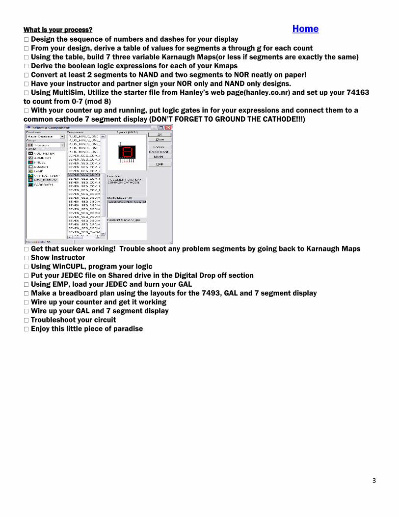
With your counter up and running, put logic gates in for your expressions and connect them to a
common cathode 7 segment display (DON’T FORGET TO GROUND THE CATHODE!!!)
Get that sucker working! Trouble shoot any problem segments by going back to Karnaugh Maps
Show instructor
Using WinCUPL, program your logic
Put your JEDEC file on Shared drive in the Digital Drop off section
Using EMP, load your JEDEC and burn your GAL
Make a breadboard plan using the layouts for the 7493, GAL and 7 segment display
Wire up your counter and get it working
Wire up your GAL and 7 segment display
Troubleshoot your circuit
Enjoy this little piece of paradise

4
Home
Activity 5.3A – Introduction to PLDs Purpose
To familiarize students with the vocabulary and background on Programmable Logic Devices (PLDs)
Procedure
Read the following information and highlight the important sections. Then answer the questions in
the conclusion section.
Programmable logic devices (PLDs) are used in many applications to replace small-scale
integration and medium-scale integration circuits. They reduce the actual number of chips needed,
the final cost buying the individual parts and the eventual cost of fabricating the circuit board. All
PLDs consist of programmable arrays: a grid of conductors that form rows and columns. There is a
fusible link at each connect point. These arrays can be re-programmable or, once programmed,
permanently fused – based on the architecture of the chip.
There are 4 basic types of PLDs:
PROM – Programmable Read-Only Memory
This PLD consists of a non-programmable AND gate array and a programmable OR array.
This device is used primarily as an addressable memory and not as a logic device
because of the limitations imposed by the fixed AND gates.
PLA – Programmable Logic Array
This PLD has both a programmable logic AND array and a programmable logic OR array.
The PLA was developed to overcome some of the limitations of the PROM. As a trade-off,
the PLAs have longer delays due to the 2 sets of fusible links from using 2 programmable
arrays and more complex circuitry.
PAL – Programmable Array Logic
Pals were developed to try and speed up the PLA chips. This PLD has a programmable
AND array and a fixed OR array with output logic. The PAL is the most common 1-time
programmable logic device and it too uses links which become permanently fused.
GAL – Generic Array Logic
The GAL is much like the PAL – it has a programmable AND array and a fixed OR array.
The primary difference is that the GAL can be reprogrammed due to the fact that it uses
E2CMOS (Electrically Erasable CMOS) instead of permanently fusing links.
Because the GAL is so versatile and can be reused over and over again it is a chip that is commonly
found and used. This structure allows any sum-of-products (SOP) logic expression with a defined
number of variables to be implemented. This chip is basically a grid of connectors forming rows
and columns with an electrically erasable CMOS cell at each cross point rather than a fuse as in a
PAL. A cell that is “on” connects the intersection point of its row and column; one that is “off”
disconnects the row and the column.

5
The standard part numbering system for a GAL chip is as follows:
The part always begins with “GAL”, followed by a 2-digit number which indicates the number of
inputs, the letter V (to designate a variable-input configuration), and lastly a 1 or 2 digit number
that is the number of outputs. Therefore the chip GAL22v10 is: Generic Array Logic, 22 inputs,
Variable output configuration and 10 outputs.
There are three components needed to program a PLD. They are:
A personal computer
a programming software (a compiler)
and, a software driven programmer
There are various types of logic compilers, all of which perform a similar function: they process and
synthesize the logic design, convert the entered data into an intermediate file and then generate a
final output file called a JEDEC file (also called a fuse or cell map).
Some examples of PLD languages are:
CUPL (Universal Compiler for Programmable Logic),
ABEL (Advanced Boolean Expression Language)
Palasm (whose letters don’t form any type of abbreviation)
The programmer used has a zip socket (zero-insertion-force), and uses the JEDEC file created by the
compiler. (JEDEC stands for Joint Electronic Device Engineering Council, the group who creates the
standard that all compilers and logic programmers use.)
Conclusion
What is the difference between a PAL and a PLA?
What does GAL stand for?
How many inputs and how many outputs does a GAL16v8 have?
What is required to program a PLD?
What is a JEDEC file?

6
Home
Activity 5.3B – A Basic Problem Purpose
To understand and apply the steps necessary to program a PLD
To understand and apply the programming syntax of the WinCUPL language
To understand and apply the steps needed to program a programmable IC
Equipment
ICs: gal22v10D
EMP 11
Breadboard and jumper wires
LEDs and current limiting resistors
5 volt power supply
Switches
Procedure
The intent of this activity is to use it as you would a tutorial. At the end you will have a programmed
chip to breadboard, test and demonstrate its function to your instructor.
The Basics:
The sequence for programming a PLD is as follows:
Design the logic circuit by creating a truth table or logic schematic
Write a series of Boolean equations in a SOP (Sum of Products) form. (Please note: it is
also possible to program the compiler using truth tables or schematic diagrams, we will
only be using Boolean equations.)
Enter preliminary information into the compiler such as name, description of project, chip
being used, description of design, number of input pins, number of output pins
Enter pin assignments and associated variable names
Enter the equations into the compiler program
Compile and check the entered program for syntax errors. The program creates the JEDEC
file.
Enter the JEDEC file into the programmer
Program the chip
Breadboard and test
7
The Compiler Program: WinCUPL
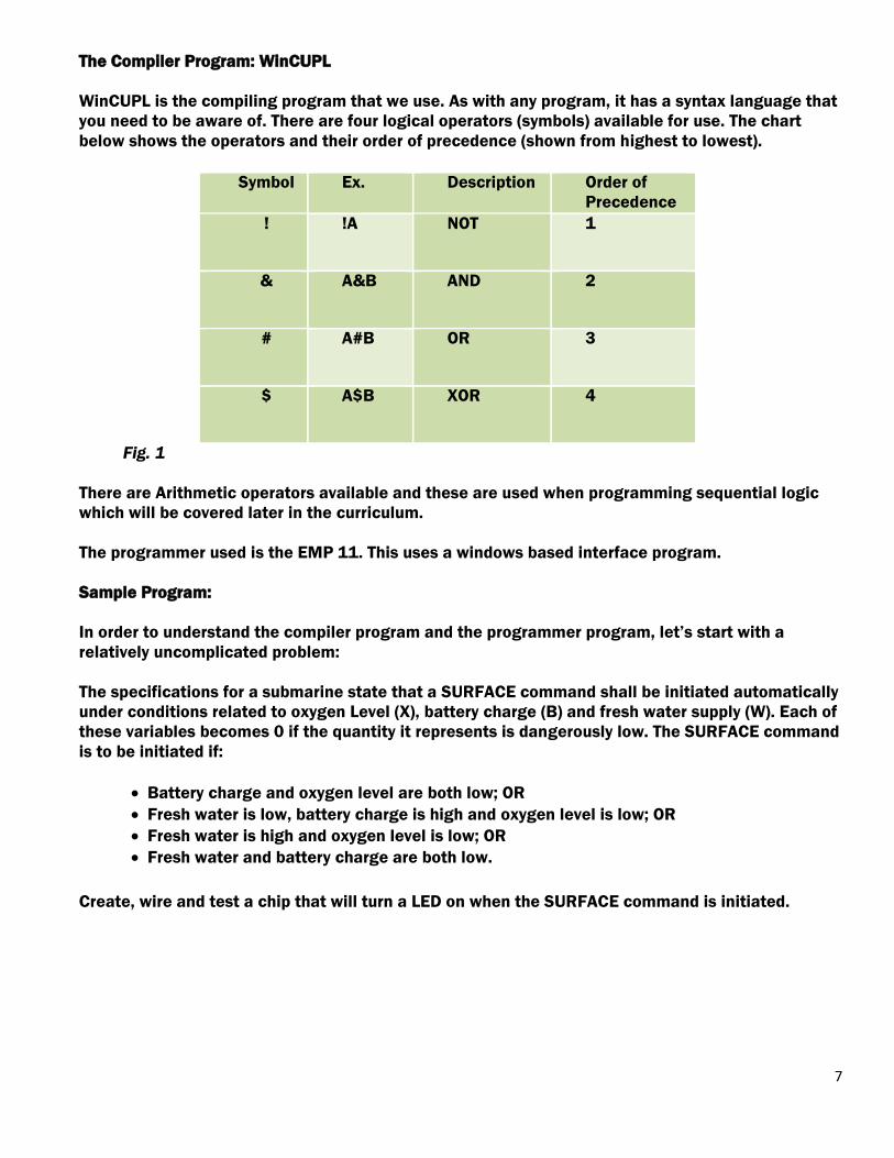
WinCUPL is the compiling program that we use. As with any program, it has a syntax language that
you need to be aware of. There are four logical operators (symbols) available for use. The chart
below shows the operators and their order of precedence (shown from highest to lowest).
Symbol Ex. Description Order of
Precedence
! !A NOT 1
& A&B AND 2
# A#B OR 3
$ A$B XOR 4
Fig. 1
There are Arithmetic operators available and these are used when programming sequential logic
which will be covered later in the curriculum.
The programmer used is the EMP 11. This uses a windows based interface program.
Sample Program:
In order to understand the compiler program and the programmer program, let’s start with a
relatively uncomplicated problem:
The specifications for a submarine state that a SURFACE command shall be initiated automatically
under conditions related to oxygen Level (X), battery charge (B) and fresh water supply (W). Each of
these variables becomes 0 if the quantity it represents is dangerously low. The SURFACE command
is to be initiated if:
Battery charge and oxygen level are both low; OR
Fresh water is low, battery charge is high and oxygen level is low; OR
Fresh water is high and oxygen level is low; OR
Fresh water and battery charge are both low.
Create, wire and test a chip that will turn a LED on when the SURFACE command is initiated.
8
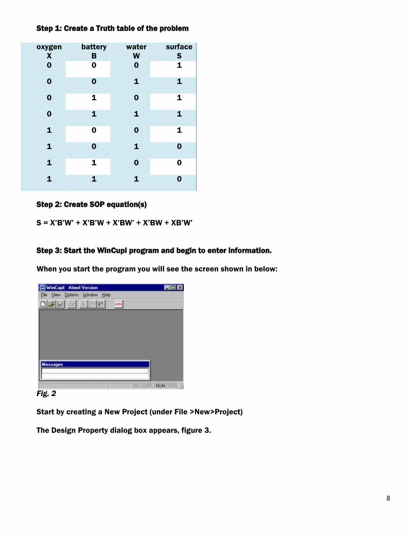
Step 1: Create a Truth table of the problem
oxygen
X
battery
B
water
W
surface
S
0 0 0 1
0 0 1 1
0 1 0 1
0 1 1 1
1 0 0 1
1 0 1 0
1 1 0 0
1 1 1 0
Step 2: Create SOP equation(s)
S = X’B’W’ + X’B’W + X’BW’ + X’BW + XB’W’
Step 3: Start the WinCupl program and begin to enter information.
When you start the program you will see the screen shown in below:
Fig. 2
Start by creating a New Project (under File >New>Project)
The Design Property dialog box appears, figure 3.

9
Fig. 3
The Name specified is the name that the project will be saved under. (Hint: This part of the program
goes back to old DOS rules, therefore you need to choose a name which is less than 8 characters in
length and has no spaces.)
Designer: Enter your name
Device: Enter g22v10 (This is the chip that we will later be programming.)
Fig. 4 Completed Dialog Box
Click ok.
Next you will see 3 dialog boxes appear.
The first will be the number of inputs. Enter 3
The second will be the number of outputs. Enter 1
The last is the number of pinnodes. Enter 0
(The gal22v10 does not support pinnodes.)
Click OK after each dialog box.
10
The compiler program will look like Figure 5.
Fig. 5
Notice that there are 3 spots under the Input Pins, and 1 spot under the Output Pin. These are the
sections where we will specify the pins to use and the variable names assigned. After the semi-
colon is a place to enter comments, which is a good programming practice.
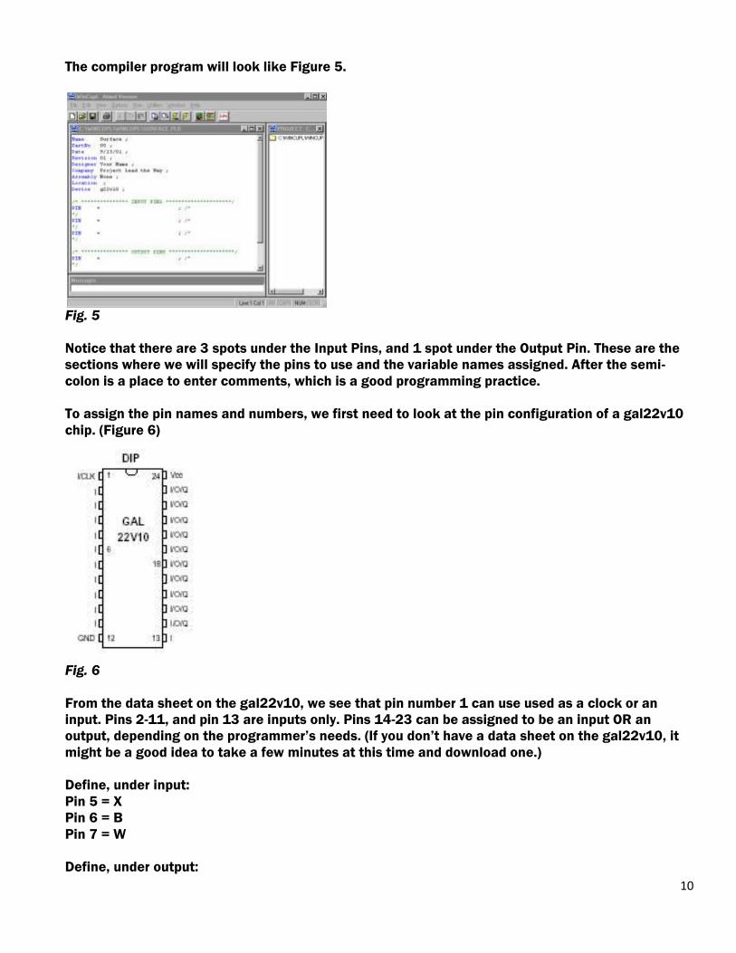
To assign the pin names and numbers, we first need to look at the pin configuration of a gal22v10
chip. (Figure 6)
Fig. 6
From the data sheet on the gal22v10, we see that pin number 1 can use used as a clock or an
input. Pins 2-11, and pin 13 are inputs only. Pins 14-23 can be assigned to be an input OR an
output, depending on the programmer’s needs. (If you don’t have a data sheet on the gal22v10, it
might be a good idea to take a few minutes at this time and download one.)
Define, under input:
Pin 5 = X
Pin 6 = B
Pin 7 = W
Define, under output:
11
Pin 18 = S
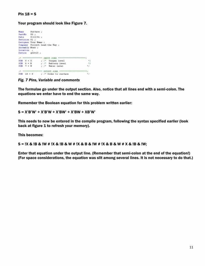
Your program should look like Figure 7.
Fig. 7 Pins, Variable and comments
The formulae go under the output section. Also, notice that all lines end with a semi-colon. The
equations we enter have to end the same way.
Remember the Boolean equation for this problem written earlier:
S = X’B’W’ + X’B’W + X’BW’ + X’BW + XB’W’
This needs to now be entered in the compile program, following the syntax specified earlier (look
back at figure 1 to refresh your memory).
This becomes:
S = !X & !B & !W # !X & !B & W # !X & B & !W # !X & B & W # X & !B & !W;
Enter that equation under the output line. (Remember that semi-colon at the end of the equation!)
(For space considerations, the equation was slit among several lines. It is not necessary to do that.)
12
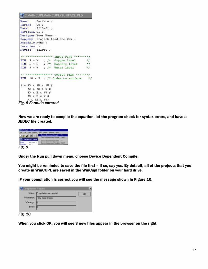
Fig. 8 Formula entered
Now we are ready to compile the equation, let the program check for syntax errors, and have a
JEDEC file created.
Fig. 9
Under the Run pull down menu, choose Device Dependent Compile.
You might be reminded to save the file first – if so, say yes. By default, all of the projects that you
create in WinCUPL are saved in the WinCupl folder on your hard drive.
IF your compilation is correct you will see the message shown in Figure 10.
Fig. 10
When you click OK, you will see 3 new files appear in the browser on the right.
13
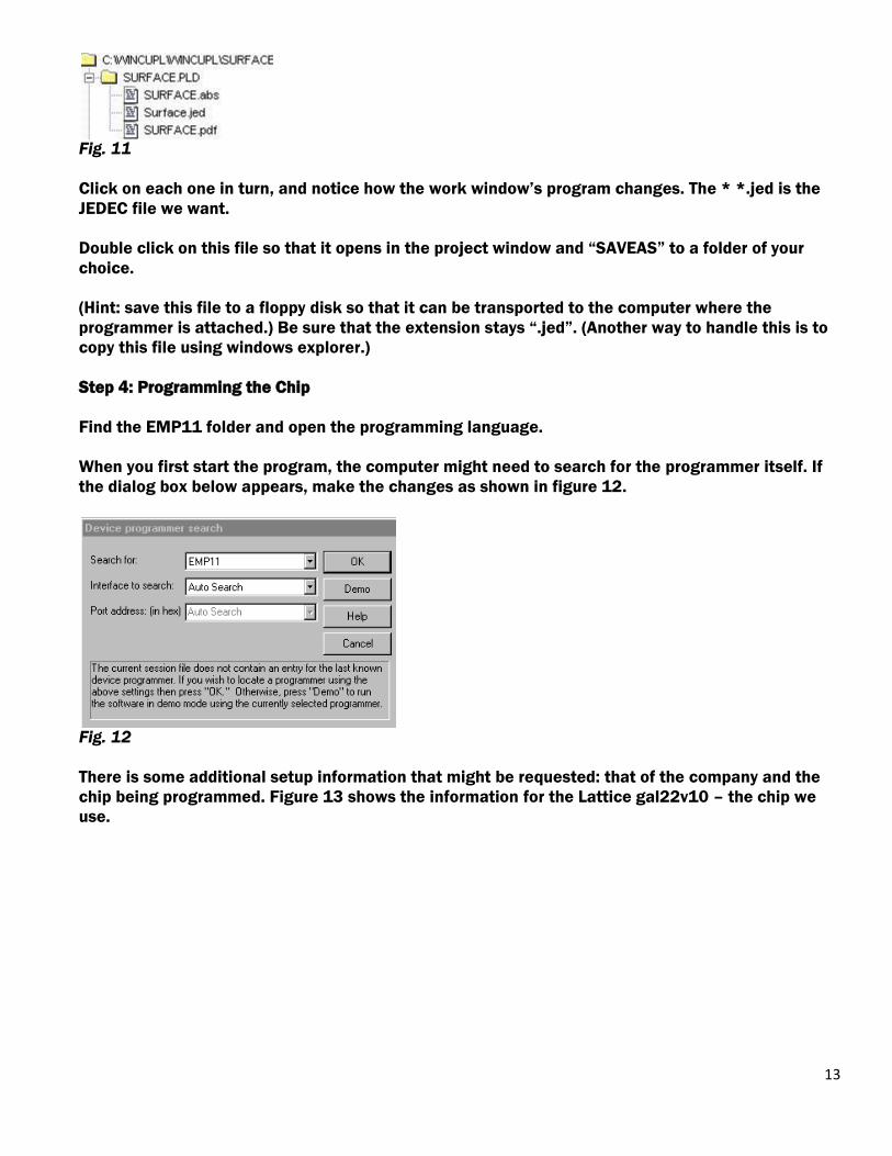
Fig. 11
Click on each one in turn, and notice how the work window’s program changes. The * *.jed is the
JEDEC file we want.
Double click on this file so that it opens in the project window and “SAVEAS” to a folder of your
choice.
(Hint: save this file to a floppy disk so that it can be transported to the computer where the
programmer is attached.) Be sure that the extension stays “.jed”. (Another way to handle this is to
copy this file using windows explorer.)
Step 4: Programming the Chip
Find the EMP11 folder and open the programming language.
When you first start the program, the computer might need to search for the programmer itself. If
the dialog box below appears, make the changes as shown in figure 12.
Fig. 12
There is some additional setup information that might be requested: that of the company and the
chip being programmed. Figure 13 shows the information for the Lattice gal22v10 – the chip we
use.
14
Fig. 13
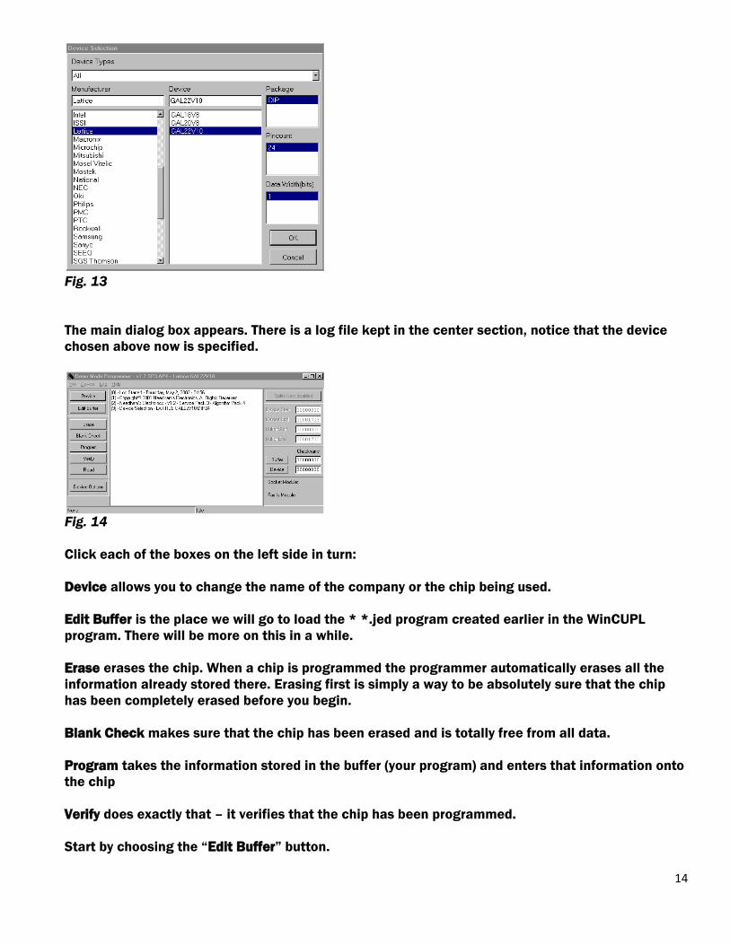
The main dialog box appears. There is a log file kept in the center section, notice that the device
chosen above now is specified.
Fig. 14
Click each of the boxes on the left side in turn:
Device allows you to change the name of the company or the chip being used.
Edit Buffer is the place we will go to load the * *.jed program created earlier in the WinCUPL
program. There will be more on this in a while.
Erase erases the chip. When a chip is programmed the programmer automatically erases all the
information already stored there. Erasing first is simply a way to be absolutely sure that the chip
has been completely erased before you begin.
Blank Check makes sure that the chip has been erased and is totally free from all data.
Program takes the information stored in the buffer (your program) and enters that information onto
the chip
Verify does exactly that – it verifies that the chip has been programmed.
Start by choosing the “Edit Buffer” button.
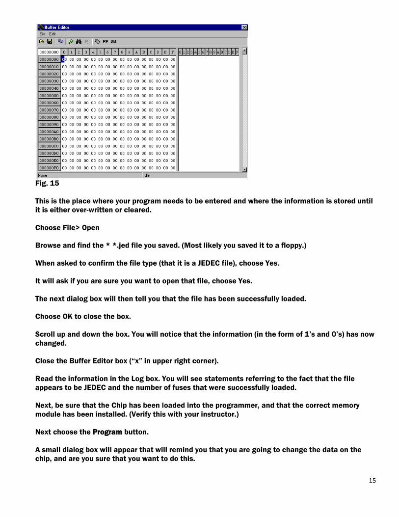
15
Fig. 15
This is the place where your program needs to be entered and where the information is stored until
it is either over-written or cleared.
Choose File> Open
Browse and find the * *.jed file you saved. (Most likely you saved it to a floppy.)
When asked to confirm the file type (that it is a JEDEC file), choose Yes.
It will ask if you are sure you want to open that file, choose Yes.
The next dialog box will then tell you that the file has been successfully loaded.
Choose OK to close the box.
Scroll up and down the box. You will notice that the information (in the form of 1’s and 0’s) has now
changed.
Close the Buffer Editor box (“x” in upper right corner).
Read the information in the Log box. You will see statements referring to the fact that the file
appears to be JEDEC and the number of fuses that were successfully loaded.
Next, be sure that the Chip has been loaded into the programmer, and that the correct memory
module has been installed. (Verify this with your instructor.)
Next choose the Program button.
A small dialog box will appear that will remind you that you are going to change the data on the
chip, and are you sure that you want to do this.

16
Choose Yes
The information will now be transferred to the chip from the programmer.
Remove the chip from its socket.
Breadboard the circuit and be sure that it performs as it was intended.
Test that the chip correctly matches the information in the established truth table above.
Demonstrate the operation of the circuit to your teacher and get signature:
_____________________________________________________________
Conclusion
Write the Boolean expression shown as if it were to be entered into the compiler: A’BC + ABC’ + AB’C’

17
Home
Problem 2.3.2 Date of Birth
Introduction
In your digital electronics class of 20, there is a 6.8% probability that two of you share the same
date of birth. This is assuming that you are all the same year level (sophomore/junior). If you are
not, the probability would be even lower.
Your date of birth makes you unique. We are going to use this uniqueness to design a circuit that
will display your date of birth on a single seven-segment display. Admittedly, this design does not
have any real practical application, but is a fun exercise that will bring together all of the design
techniques that you have learned in this lesson.
Your date of birth may make you unique in your class, but in 2006 there were 263,898,574,096
births world-wide. This means that on a daily basis, over 700,000,000 individuals share the same
date of birth.
Equipment
Paper & Pencil
Circuit Design Software (CDS)
Digital Logic Board (DLB)
Common Cathode Seven-Segment Display
Jumper Wire
Procedure
Design
Design a combinational logic circuit that has three inputs and seven outputs. As the inputs (X, Y,
and Z) count from 000 to 111, the seven outputs (a) thru (g) will generate the logic required to
display your date of birth on a seven-segment display. The date of birth will be displayed in the MM-
DD-YY format. For example if you were born on May 12, 1993, your design will display 05-12-93.

18
Detail Design Specification:
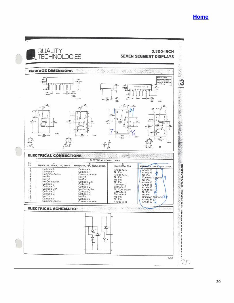
The seven-segment display must be a common cathode.
Current limiting resistors (330) must be used.
The Karnaugh mapping technique must be used to obtain the simplified logic expression for
each of the seven segments.
At least two segments must be implemented with NAND only logic.
At least two segments must be implemented with NOR only logic.
The implementation of the remaining segments is left to your discretion.
Simulation
Using the Circuit Design Software (CDS), enter and test your Date of Birth design. Use the 74163
for the inputs X, Y, & Z. Verify that the circuit is working as designed. If the circuit is not working
properly, review your design work and circuit implementation to identify your mistake. Make any
necessary corrections and retest. Be sure to document all changes in your engineering
notebook/portfolio.
Prototyping
Using the Digital Logic Board (DLB), build and test your Date of Birth design. Verify that the circuit
is working as designed. If it is not, DO NOT CHANGE YOUR DESIGN. You know that your design is
good because you simulated it. If your circuit isn’t working correctly, you must have built something
incorrectly. Review your circuit implementation to identify your mistakes, make the necessary
corrections, and retest. Be sure to document all changes in your engineering notebook.
19
Home
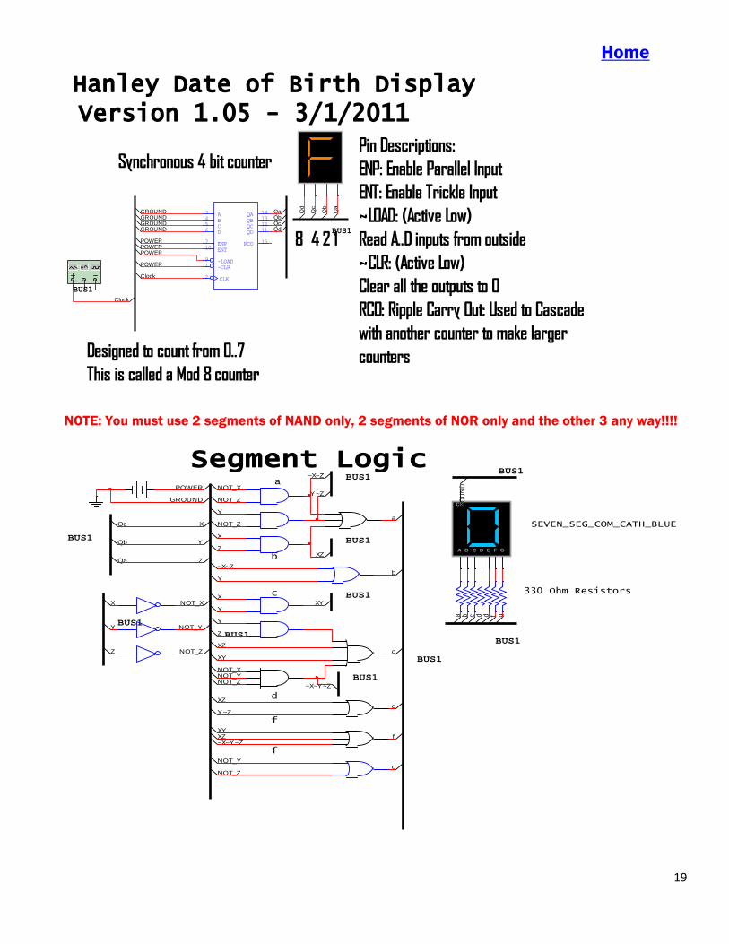
NOTE: You must use 2 segments of NAND only, 2 segments of NOR only and the other 3 any way!!!!
Hanley Date of Birth Display
QA 14
QB 13
QC 12
QD 11
RCO 15
A3
B4
C5
D6
ENP7
ENT10
~LOAD9
~CLR1
CLK2
Synchronous 4 bit counter
Designed to count from 0..7
This is called a Mod 8 counter
GROUNDGROUNDGROUNDGROUND
Clock
Pin Descriptions:
ENP: Enable Parallel Input
ENT: Enable Trickle Input
~LOAD: (Active Low)
Read A..D inputs from outside
~CLR: (Active Low)
Clear all the outputs to 0
RCO: Ripple Carry Out: Used to Cascade
with another counter to make larger
counters
BUS1
QaQbQcQd BUS1
Qd
Qc
Qb
Qa
POWERPOWER
8 4 2 1
Clock
POWER
POWER
Version 1.05 - 3/1/2011
BUS1
A B C D E F G
CK
POWER
GROUND
BUS1
X
Y
Z
NOT_X
NOT_Z
Y
NOT_Z
X
Z
BUS1
BUS1
a
b
c
a
BUS1~X~Z
~X~Z
Y
BUS1
a
b
BUS1
XZ
X
Y
BUS1XY
Z
Y
GR
OU
ND
XZ
XY
NOT_XNOT_YNOT_Z
c
dXZ
Y~Z
Y~Zd
b c d d
f
fXYXZ
BUS1~X~Y~Z
~X~Y~Z
f
fNOT_Y
NOT_Zg
g
Segment Logic
BUS1
XQc
Qb Y
Qa Z
330 Ohm Resistors
SEVEN_SEG_COM_CATH_BLUE
NOT_X
NOT_Y
NOT_Z
20
Home

21
Home

22
Home

23
Home
Writing up a Report Write a report summarizing the date of birth project.
Start your report with a nifty cover page. (Note cover pages and table of contents are NOT
numbered)
Next create a table of contents. Your table of contents must have both sides aligned so that each
margin is “clean” and not jagged.
A good way to do this is to use a right justified tab (After placing a tab on the ruler using MS Word,
double click on the symbol. Make sure that the tab goes with the right angle to the right)
This will allow you to make a table of contents where both left and right sides are clean.
Then create a page that has a problem statement. What is it that you were trying to
accomplish? (This is the first page that should be numbered) What is the date of birth you were
going to display?
Include your truth table typed and all of your Karnaugh Maps typed. (You may solve them neatly
with pencil or pen if desired)
Next page is the MultiSim Circuit : Hint a screen shot would be great here
Now we are ready for WinCUPL, copy paste might be the best approach
Your breadboard plan can be folded and stapled in next
Now you can paste in a picture of your breadboarded circuit(Zoom in and annotate) which chip
does what
Concluding paragraph of where you had difficulties and why

24
Rubric for Date of Birth Problem: Home
Name______________________________________
Ok, so clip art collection is a little lean!!
Task Points Given
Checkpoint for 7 segment display driver
circuit working on computer
30
Above circuit neat, well documented 10
Breadboard Plan 35
Demonstrate working 74163 mod 6, 7
or 8 counter
25
Demonstrate working DOB 7 segment
display on breadboard
50
Written report (with page numbers,
stapled or bound)
0
-Title page (typed) 10
-Table contents (typed) 10
-Problem statement (typed) 10
-Truth table (typed) 10
-Kmaps solved (NEAT) 10
-Printed copy of your circuit 10
-Breadboard plan 10
-Picture of your circuit annotated 10
-Concluding paragraph of where you had
difficulties and why
10
-Page numbering 10

25
TOTAL 230