DIFFERENTIAL-TO-LVDS/0.7V DIFFERENTIAL...
19
DIFFERENTIAL-TO-LVDS/0.7V DIFFERENTIAL PCI EXPRESS™ JITTER ATTENUATOR ICS8741004 IDT™ / ICS™ PCI EXPRESS™ JITTER ATTENUATOR 1 ICS8741004AG REV. ANOVEMBER 1, 2007 General Description The ICS8741004 is a high performance Differential-to-LVDS/0.7V Differential Jitter Attenuator designed for use in PCI Express™ systems. In some PCI Express systems, such as those found in desktop PCs, the PCI Express clocks are generated from a low bandwidth, high phase noise PLL frequency synthesizer. In these systems, a jitter attenuator may be required to attenuate high frequency random and deterministic jitter components from the PLL synthesizer and from the system board. The ICS8741004 has 3 PLL bandwidth modes: 200kHz, 600kHz and 2MHz. The 200kHz mode will provide maximum jitter attenuation, but with higher PLL tracking skew and spread spectrum modulation from the motherboard synthesizer may be attenuated. The 600kHz provides an intermediate bandwidth that can easily track triangular spread profiles, while providing good jitter attenuation. The 2MHz bandwidth provides the best tracking skew and will pass most spread profiles, but the jitter attenuation will not be as good as the lower bandwidth modes. Because some 2.5Gb serdes have x20 multipliers while others have x25 multipliers, the ICS8741004 can be set for 1:1 mode or 5/4 multiplication mode (i.e. 100MHz input/125MHz output) using the F_SEL pins. The ICS8741004 uses IDT’s 3 rd Generation FemtoClock™ PLL technology to achieve the lowest possible phase noise. The device is packaged in a 24 Lead TSSOP package, making it ideal for use in space constrained applications such as PCI Express add-in cards. PLL Bandwidth Features • Two LVDS and two 0.7V differential output pairs Bank A has two LVDS output pairs and Bank B has two 0.7V differential output pairs • One differential clock input pair • CLK, CLK pair can accept the following differential input levels: LVPECL, LVDS, LVHSTL, SSTL, HCSL • Output frequency range: 98MHz - 160MHz • Input frequency range: 98MHz - 128MHz • VCO range: 490MHz - 640MHz • Cycle-to-cycle jitter: 35ps (maximum) • Full 3.3V operating supply • Three bandwidth modes allow the system designer to make jitter attenuation/tracking skew design trade-offs • 0°C to 70°C ambient operating temperature • Available in both standard (RoHS 5) and lead-free (RoHS 6) packages Pin Assignment ICS8741004 24-Lead TSSOP 4.4mm x 7.8mm x 0.925mm package body G Package Top View BW_SEL 0 = PLL Bandwidth: ~200kHz Float = PLL Bandwidth: ~600kHz (default) 1 = PLL Bandwidth: ~2MHz HiPerClockS™ ICS 1 2 3 4 5 6 7 8 9 10 11 12 24 23 22 21 20 19 18 17 16 15 14 13 nQA1 QA1 V DDO QA0 nQA0 MR BW_SEL nc V DDA F_SELA V DD OEA nQB1 QB1 V DDO QB0 nQB0 IREF F_SELB OEB GND GND nCLK CLK
Transcript of DIFFERENTIAL-TO-LVDS/0.7V DIFFERENTIAL...

DIFFERENTIAL-TO-LVDS/0.7V DIFFERENTIAL PCI EXPRESS™ JITTER ATTENUATOR
ICS8741004
IDT™ / ICS™ PCI EXPRESS™ JITTER ATTENUATOR 1 ICS8741004AG REV. ANOVEMBER 1, 2007
General Description
The ICS8741004 is a high performance Differential-to-LVDS/0.7V Differential Jitter Attenuator designed for use in PCI Express™ systems. In some PCI Express systems, such as those found in desktop PCs, the PCI Express clocks
are generated from a low bandwidth, high phase noise PLL frequency synthesizer. In these systems, a jitter attenuator may be required to attenuate high frequency random and deterministic jitter components from the PLL synthesizer and from the system board. The ICS8741004 has 3 PLL bandwidth modes: 200kHz, 600kHz and 2MHz. The 200kHz mode will provide maximum jitter attenuation, but with higher PLL tracking skew and spread spectrum modulation from the motherboard synthesizer may be attenuated. The 600kHz provides an intermediate bandwidth that can easily track triangular spread profiles, while providing good jitter attenuation. The 2MHz bandwidth provides the best tracking skew and will pass most spread profiles, but the jitter attenuation will not be as good as the lower bandwidth modes. Because some 2.5Gb serdes have x20 multipliers while others have x25 multipliers, the ICS8741004 can be set for 1:1 mode or 5/4 multiplication mode (i.e. 100MHz input/125MHz output) using the F_SEL pins.
The ICS8741004 uses IDT’s 3rd Generation FemtoClock™PLL technology to achieve the lowest possible phase noise.The device is packaged in a 24 Lead TSSOP package, making it ideal for use in space constrained applications such as PCI Express add-in cards.
PLL Bandwidth
Features
• Two LVDS and two 0.7V differential output pairsBank A has two LVDS output pairs andBank B has two 0.7V differential output pairs
• One differential clock input pair
• CLK, CLK pair can accept the following differential input levels: LVPECL, LVDS, LVHSTL, SSTL, HCSL
• Output frequency range: 98MHz - 160MHz
• Input frequency range: 98MHz - 128MHz
• VCO range: 490MHz - 640MHz
• Cycle-to-cycle jitter: 35ps (maximum)
• Full 3.3V operating supply
• Three bandwidth modes allow the system designer to make jitter attenuation/tracking skew design trade-offs
• 0°C to 70°C ambient operating temperature
• Available in both standard (RoHS 5) and lead-free (RoHS 6) packages
Pin Assignment
ICS874100424-Lead TSSOP
4.4mm x 7.8mm x 0.925mm package body
G PackageTop View
BW_SEL0 = PLL Bandwidth: ~200kHzFloat = PLL Bandwidth: ~600kHz (default)1 = PLL Bandwidth: ~2MHz
HiPerClockS™
ICS
12
3456789101112
2423
22212019181716151413
nQA1QA1
VDDO
QA0nQA0
MRBW_SEL
ncVDDA
F_SELAVDD
OEA
nQB1QB1VDDO
QB0nQB0IREFF_SELBOEBGNDGNDnCLKCLK

ICS8741004DIFFERENTIAL-TO-LVDS/0.7V DIFFERENTIAL PCI EXPRESS™ JITTER ATTENUATOR
IDT™ / ICS™ PCI EXPRESS™ JITTER ATTENUATOR 2 ICS8741004AG REV. ANOVEMBER 1, 2007
Block Diagram
F_SELA0 ÷5 (default)
1 ÷4
F_SELB0 ÷5 (default)
1 ÷4
VCO490 - 640 MHz
PhaseDetector
M = ÷5 (fixed)
QA0
nQA0
QA1
nQA1
Pullup
Pullup
Pulldown
Float
Pulldown
OEA
OEB
F_SELA
F_SELB
BW_SEL
CLK
nCLK
MR
IREF
Pullup
Pulldown
Pulldown
QB0
nQB0
QB1
nQB1
0 = ~200kHz
Float = ~400kHz
1 = ~800kHz

ICS8741004DIFFERENTIAL-TO-LVDS/0.7V DIFFERENTIAL PCI EXPRESS™ JITTER ATTENUATOR
IDT™ / ICS™ PCI EXPRESS™ JITTER ATTENUATOR 3 ICS8741004AG REV. ANOVEMBER 1, 2007
Table 1. Pin Descriptions
NOTE: Pullup and Pulldown refer to internal input resistors. See Table 2, Pin Characteristics, for typical values.
Table 2. Pin Characteristics
Number Name Type Description
1, 24 QA1, QA1 Output Differential output pair. LVDS interface levels.
3, 22 VDDO Power Output supply pins.
4, 5 QA0, QA0 Output Differential output pair. LVDS interface levels.
6 MR Input Pulldown
Active High Master Reset. When logic HIGH, the internal dividers are reset causing the true outputs Q[Ax:Bx] to go LOW and the inverted outputs Q[Ax:Bx] to go HIGH. When logic LOW, the internal dividers and the outputs are enabled. LVCMOS/LVTTL interface levels.
7 BW_SEL InputPullup/
PulldownPLL Bandwidth input. LVCMOS/LVTTL interface levels. See Table 3B.
8 nc Unused No connect.
9 VDDA Power Analog supply pin.
10 F_SELA Input Pulldown Frequency select pins for QAx/QAx outputs. LVCMOS/LVTTL interface levels. See Table 3C.
11 VDD Power Core supply pin.
12 OEA Input PullupOutput enable for QAx pins. When HIGH, QAx/QAx outputs are enabled. When LOW, the QAx/QAx outputs are in a high impedance state. LVCMOS/LVTTL interface levels. See Table 3A.
13 CLK Input Pulldown Non-inverting differential clock input.
14 CLK Input Pullup Inverting differential clock input.
15, 16 GND Power Power supply ground.
17 OEB Input PullupOutput enable for QBx pins. When HIGH, QBx/QBx outputs are enabled. When LOW, the QBx/QBx outputs are in a high impedance state. LVCMOS/LVTTL interface levels. See Table 3A.
18 F_SELB Input Pulldown Frequency select pins for QBx/QBx outputs. LVCMOS/LVTTL interface levels. See Table 3C.
19 IREF InputA fixed precision resistor (RREF = 475Ω) from this pin to ground provides a reference current used for differential current-mode QB0/nQB0 clock outputs.
20, 21 QB0, QB0 Output Differential output pair. HCSL interface levels.
23, 24 QB1, QB1 Output Differential output pair. HCSL interface levels.
Symbol Parameter Test Conditions Minimum Typical Maximum Units
CIN Input Capacitance 4 pF
RPULLUP Input Pullup Resistor 51 kΩ
RPULLDOWN Input Pulldown Resistor 51 kΩ
ICS8741004DIFFERENTIAL-TO-LVDS/0.7V DIFFERENTIAL PCI EXPRESS™ JITTER ATTENUATOR
IDT™ / ICS™ PCI EXPRESS™ JITTER ATTENUATOR 4 ICS8741004AG REV. ANOVEMBER 1, 2007
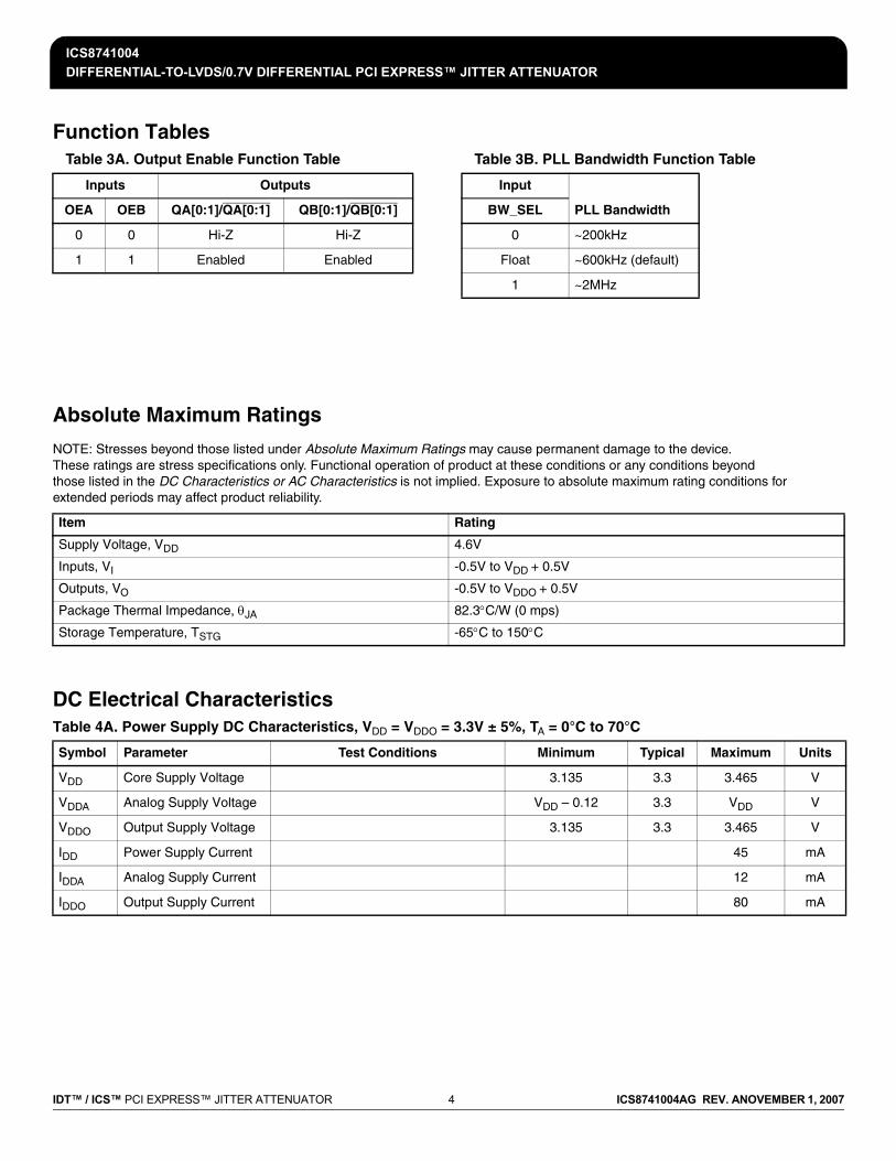
Function TablesTable 3A. Output Enable Function Table Table 3B. PLL Bandwidth Function Table
Absolute Maximum Ratings
NOTE: Stresses beyond those listed under Absolute Maximum Ratings may cause permanent damage to the device. These ratings are stress specifications only. Functional operation of product at these conditions or any conditions beyond those listed in the DC Characteristics or AC Characteristics is not implied. Exposure to absolute maximum rating conditions for extended periods may affect product reliability.
DC Electrical CharacteristicsTable 4A. Power Supply DC Characteristics, VDD = VDDO = 3.3V ± 5%, TA = 0°C to 70°C
Inputs Outputs
OEA OEB QA[0:1]/QA[0:1] QB[0:1]/QB[0:1]
0 0 Hi-Z Hi-Z
1 1 Enabled Enabled
Input
PLL BandwidthBW_SEL
0 ~200kHz
Float ~600kHz (default)
1 ~2MHz
Item Rating
Supply Voltage, VDD 4.6V
Inputs, VI -0.5V to VDD + 0.5V
Outputs, VO -0.5V to VDDO + 0.5V
Package Thermal Impedance, θJA 82.3°C/W (0 mps)
Storage Temperature, TSTG -65°C to 150°C
Symbol Parameter Test Conditions Minimum Typical Maximum Units
VDD Core Supply Voltage 3.135 3.3 3.465 V
VDDA Analog Supply Voltage VDD – 0.12 3.3 VDD V
VDDO Output Supply Voltage 3.135 3.3 3.465 V
IDD Power Supply Current 45 mA
IDDA Analog Supply Current 12 mA
IDDO Output Supply Current 80 mA

ICS8741004DIFFERENTIAL-TO-LVDS/0.7V DIFFERENTIAL PCI EXPRESS™ JITTER ATTENUATOR
IDT™ / ICS™ PCI EXPRESS™ JITTER ATTENUATOR 5 ICS8741004AG REV. ANOVEMBER 1, 2007
Table 4B. LVCMOS/LVTTL DC Characteristics, VDD = VDDO = 3.3V ± 5%, TA = 0°C to 70°C
Table 4C. Differential DC Characteristics, VDD = VDDO = 3.3V ± 5%, TA = 0°C to 70°C
NOTE 1: VIL should not be less than -0.3VNOTE 2: Common mode input voltage is defined as VIH.
Table 4D. LVDS DC Characteristics, VDD = VDDO = 3.3V ± 5%, TA = 0°C to 70°C
Symbol Parameter Test Conditions Minimum Typical Maximum Units
VIH Input High Voltage
OEA, OEB, MR, F_SELA, F_SELB
2 VDD + 0.3 V
BW_SEL VDD – 0.3 VDD + 0.3 V
VIL Input Low Voltage
OEA, OEB, MR, F_SELA, F_SELB
-0.3 0.8 V
BW_SEL -0.3 +0.3 V
VIM Input Mid Voltage BW_SEL VDD/2 – 0.1 VDD/2 + 0.1 V
IIH Input High Current
F_SELA, F_SELB, MR, BW_SEL
VDD = VIN = 3.465V 150 µA
OEA, OEB VDD = VIN = 3.465V 5 µA
IIL Input Low Current
MR,F_SELA, F_SELB,
VDD = 3.465V, VIN = 0V -5 µA
OEA, OEB, BW_SEL VDD = 3.465V, VIN = 0V -150 µA
Symbol Parameter Test Conditions Minimum Typical Maximum Units
IIH Input High CurrentCLK VDD = VIN = 3.465V 150 µA
CLK VDD = VIN = 3.465V 5 µA
IIL Input Low Current
CLKVDD = 3.465V,
VIN = 0V-5 µA
CLKVDD = 3.465V,
VIN = 0V-150 µA
VPP Peak-to-Peak Voltage; NOTE 1 0.15 1.3 V
VCMR Common Mode Input Voltage; NOTE 1, 2 GND + 0.5 VDD – 0.85 V
Symbol Parameter Test Conditions Minimum Typical Maximum Units
VOD Differential Output Voltage 290 390 490 mV
∆VOD VOD Magnitude Change 50 mV
VOS Offset Voltage 1.2 1.35 1.5 V
∆VOS VOS Magnitude Change 50 mV

ICS8741004DIFFERENTIAL-TO-LVDS/0.7V DIFFERENTIAL PCI EXPRESS™ JITTER ATTENUATOR
IDT™ / ICS™ PCI EXPRESS™ JITTER ATTENUATOR 6 ICS8741004AG REV. ANOVEMBER 1, 2007
AC Electrical CharacteristicsTable 5. 0.7V Differential AC Characteristics, VDD = VDDO = 3.3V ± 5%, TA = 0°C to 70°C
NOTE 1: This parameter is defined in accordance with JEDEC Standard 65.NOTE 2: Defined as skew within a bank of outputs at the same voltage and with equal load conditions.
Parameter Symbol Test Conditions Minimum Typical Maximum Units
fMAX Output Frequency 98 160 MHz
tjit(cc) Cycle-to-Cycle Jitter; NOTE 1 35 ps
tsk(b) Bank Skew, NOTE 2 30 ps
VHIGH Output Voltage High QBx/QBx 530 870 mV
VLOW Output Voltage Low QBx/QBx -150 mV
VOVS Max. Voltage, Overshoot QBx/QBx VHIGH + 0.35 V
VUDS Min. Voltage, Undershoot QBx/QBx -0.3 V
Vrb Ringback Voltage QBx/QBx 0.2 V
VCROSS Absolute Crossing Voltage QBx/QBx @ 0.7V Swing 250 550 mV
∆VCROSSTotal Variation of VCROSS over all edges
QBx/QBx @ 0.7V Swing 140 mV
tR / tF Output Rise/Fall TimeQBx/QBx
measured between 0.175V to 0.525V
175 700 ps
QAx/QAx 20% to 80% 250 600 ps
∆tR / ∆tF Rise/Fall Time Variation QBx/QBx 125 ps
tRFM Rise/Fall Matching QBx/QBx 20 %
odc Output Duty Cycle 48 52 %

ICS8741004DIFFERENTIAL-TO-LVDS/0.7V DIFFERENTIAL PCI EXPRESS™ JITTER ATTENUATOR
IDT™ / ICS™ PCI EXPRESS™ JITTER ATTENUATOR 7 ICS8741004AG REV. ANOVEMBER 1, 2007
Parameter Measurement Information
3.3V HCSL Output Load AC Test Circuit
Differential Input Level
Cycle-to-Cycle Jitter
3.3V LVDS Output Load AC Test Circuit
Bank Skew
Output Duty Cycle/Pulse Width/Period
RREF = 475Ω
Measurement Point33Ω 50Ω
50Ω33ΩMeasurement
Point
49.9Ω
49.9Ω
HCSL
GND2pF
2pF
VDDA
VDD,,
VDDO
CLK
CLK
VDD
GND
VOS
Cross Points VOD
tcycle n tcycle n+1
tjit(cc) = tcycle n – tcycle n+11000 Cycles
QA[0:1],QB[0:1]
QA[0:1],QB[0:1]
SCOPEQx
nQx
3.3V±5% POWER SUPPLY+ –Float GND LVDS
VDDA
VDD,VDDO
tsk(b)
QX0
QX0
QX1
QX1
Where X is either Bank A or Bank B
tPW
tPERIOD
tPW
tPERIOD
odc = x 100%
QA[0:1],QB[0:1]
QA[0:1],QB[0:1]
ICS8741004DIFFERENTIAL-TO-LVDS/0.7V DIFFERENTIAL PCI EXPRESS™ JITTER ATTENUATOR
IDT™ / ICS™ PCI EXPRESS™ JITTER ATTENUATOR 8 ICS8741004AG REV. ANOVEMBER 1, 2007
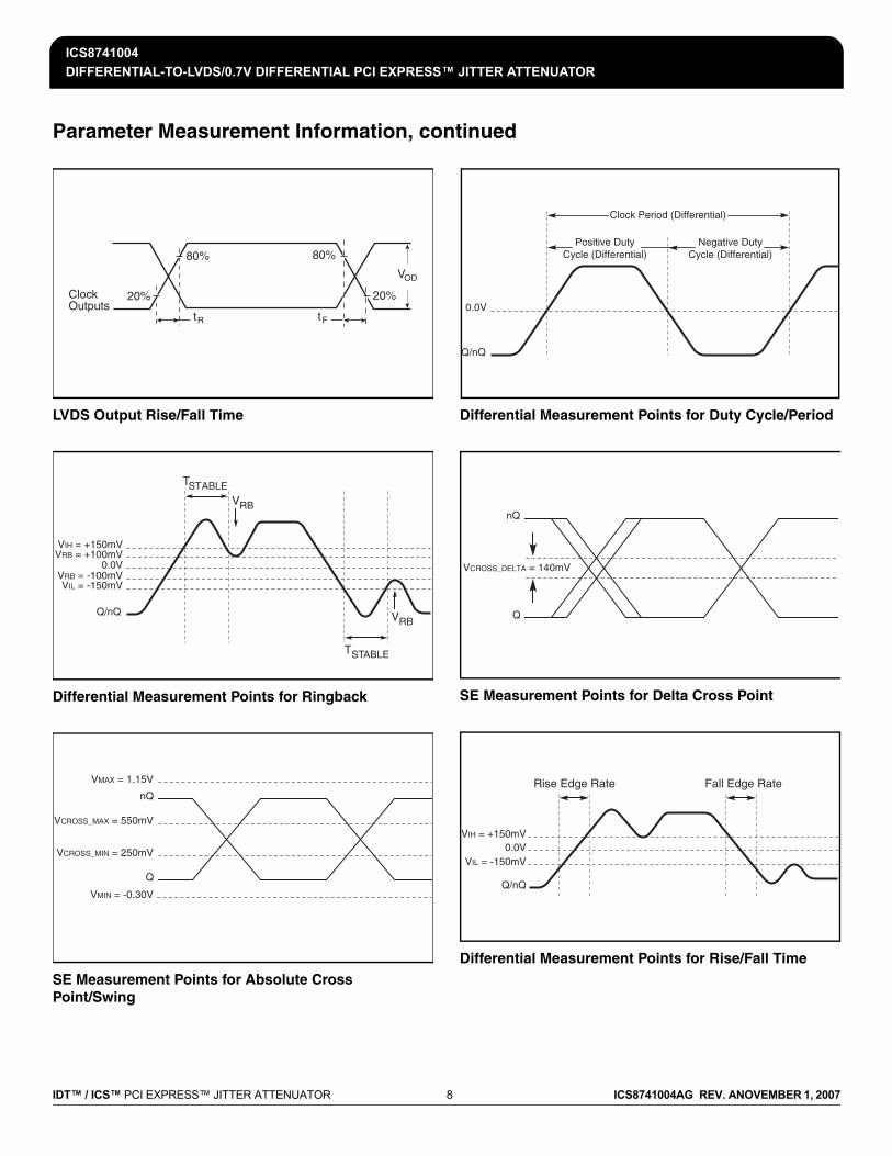
Parameter Measurement Information, continued
LVDS Output Rise/Fall Time
Differential Measurement Points for Ringback
SE Measurement Points for Absolute Cross Point/Swing
Differential Measurement Points for Duty Cycle/Period
SE Measurement Points for Delta Cross Point
Differential Measurement Points for Rise/Fall Time
Clock Outputs
20%
80% 80%
20%
tR tF
VOD
TSTABLE
TSTABLE
VRB
VRBQ/nQ
VIL = -150mVVRB = -100mV
VRB = +100mVVIH = +150mV
0.0V
nQ
Q
VCROSS_MAX = 550mV
VCROSS_MIN = 250mV
VMAX = 1.15V
VMIN = -0.30V
Q/nQ
0.0V
Positive Duty Cycle (Differential)
Negative Duty Cycle (Differential)
Clock Period (Differential)
Q
nQ
VCROSS_DELTA = 140mV
Rise Edge Rate Fall Edge Rate
Q/nQ
VIL = -150mV
VIH = +150mV0.0V
ICS8741004DIFFERENTIAL-TO-LVDS/0.7V DIFFERENTIAL PCI EXPRESS™ JITTER ATTENUATOR
IDT™ / ICS™ PCI EXPRESS™ JITTER ATTENUATOR 9 ICS8741004AG REV. ANOVEMBER 1, 2007
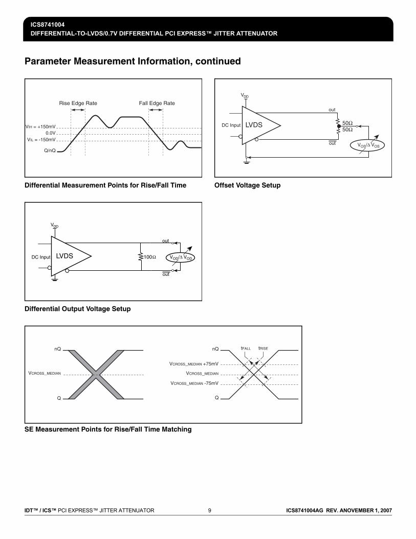
Parameter Measurement Information, continued
Differential Measurement Points for Rise/Fall Time
Differential Output Voltage Setup
Offset Voltage Setup
SE Measurement Points for Rise/Fall Time Matching
Rise Edge Rate Fall Edge Rate
Q/nQ
VIL = -150mV
VIH = +150mV0.0V
100
out
out
LVDSDC Input VOD/∆ VOD
VDD
out
out
LVDSDC Input
VOS/∆ VOS
VDD
nQ
Q
VCROSS_MEDIAN
nQ
Q
VCROSS_MEDIAN
VCROSS_MEDIAN +75mV
VCROSS_MEDIAN -75mV
tFALL tRISE

ICS8741004DIFFERENTIAL-TO-LVDS/0.7V DIFFERENTIAL PCI EXPRESS™ JITTER ATTENUATOR
IDT™ / ICS™ PCI EXPRESS™ JITTER ATTENUATOR 10 ICS8741004AG REV. ANOVEMBER 1, 2007
Application Information
Power Supply Filtering Technique
As in any high speed analog circuitry, the power supply pins are vulnerable to random noise. To achieve optimum jitter performance, power supply isolation is required. The ICS8741004 provides separate power supplies to isolate any high switching noise from the outputs to the internal PLL. VDD, VDDA and VDDO should be individually connected to the power supply plane through vias, and 0.01µF bypass capacitors should be used for each pin. Figure 1 illustrates this for a generic VDD pin and also shows that VDDA requires that an additional 10Ω resistor along with a 10µF bypass capacitor be connected to the VDDA pin. Figure 1. Power Supply Filtering
Wiring the Differential Input to Accept Single Ended Levels
Figure 2 shows how the differential input can be wired to accept single ended levels. The reference voltage V_REF = VDD/2 is generated by the bias resistors R1, R2 and C1. This bias circuit should be located as close as possible to the input pin. The ratio of
R1 and R2 might need to be adjusted to position the V_REF in the center of the input voltage swing. For example, if the input clock swing is only 2.5V and VDD = 3.3V, V_REF should be 1.25V and R2/R1 = 0.609.
Figure 2. Single-Ended Signal Driving Differential Input
VDD
VDDA
3.3V
10Ω
10µF.01µF
.01µF
V_REF
Single Ended Clock Input
VDD
CLK
nCLK
R11K
C10.1u R2
1K

ICS8741004DIFFERENTIAL-TO-LVDS/0.7V DIFFERENTIAL PCI EXPRESS™ JITTER ATTENUATOR
IDT™ / ICS™ PCI EXPRESS™ JITTER ATTENUATOR 11 ICS8741004AG REV. ANOVEMBER 1, 2007
Differential Clock Input Interface
The CLK /nCLK accepts LVDS, LVPECL, LVHSTL, SSTL, HCSL and other differential signals. Both VSWING and VOH must meet the VPP and VCMR input requirements. Figures 3A to 3F show interface examples for the HiPerClockS CLK/nCLK input driven by the most common driver types. The input interfaces suggested here are examples only. Please consult with the vendor of the driver
component to confirm the driver termination requirements. For example, in Figure 3A, the input termination applies for IDT HiPerClockS open emitter LVHSTL drivers. If you are using an LVHSTL driver from another vendor, use their termination recommendation.
Figure 3A. HiPerClockS CLK/nCLK Input Driven by an IDT Open Emitter HiPerClockS LVHSTL Driver
Figure 3C. HiPerClockS CLK/nCLK InputDriven by a 3.3V LVPECL Driver
Figure 3E. HiPerClockS CLK/nCLK InputDriven by a 3.3V HCSL Driver
Figure 3B. HiPerClockS CLK/nCLK Input Driven by a 3.3V LVPECL Driver
Figure 3D. HiPerClockS CLK/nCLK InputDriven by a 3.3V LVDS Driver
Figure 3F. HiPerClockS CLK/nCLK InputDriven by a 2.5V SSTL Driver
R150
R250
1.8V
Zo = 50Ω
Zo = 50Ω
CLK
nCLK
3.3V
LVHSTL
IDTHiPerClockS LVHSTL Driver
HiPerClockSInput
R3125
R4125
R184
R284
3.3V
Zo = 50Ω
Zo = 50Ω
CLK
nCLK
3.3V3.3V
LVPECL HiPerClockSInput
HCSL
*R3 33
*R4 33
CLK
nCLK
2.5V 3.3V
Zo = 50Ω
Zo = 50Ω
HiPerClockSInputR1
50R250
*Optional – R3 and R4 can be 0Ω
CLK
nCLKHiPerClockS Input
LVPECL
3.3V
Zo = 50Ω
Zo = 50Ω
3.3V
R150
R250
R250
3.3V
R1100
LVDS
CLK
nCLK
3.3V
Receiver
Zo = 50Ω
Zo = 50Ω
CLK
nCLKHiPerClockS
SSTL
2.5V
Zo = 60Ω
Zo = 60Ω
2.5V
3.3V
R1120
R2120
R3120
R4120

ICS8741004DIFFERENTIAL-TO-LVDS/0.7V DIFFERENTIAL PCI EXPRESS™ JITTER ATTENUATOR
IDT™ / ICS™ PCI EXPRESS™ JITTER ATTENUATOR 12 ICS8741004AG REV. ANOVEMBER 1, 2007
Recommendations for Unused Input and Output Pins
Inputs:
LVCMOS Control PinsAll control pins have internal pull-ups or pull-downs; additional resistance is not required but can be added for additional protection. A 1kΩ resistor can be used.
Outputs:
Differential OutputsAll unused differential outputs can be left floating. We recommend that there is no trace attached. Both sides of the differential output pair should either be left floating or terminated.
LVDS OutputsAll unused LVDS output pairs can be either left floating or terminated with 100Ω across. If they are left floating, we recommend that there is no trace attached.
LVDS Driver Termination
A general LVDS interface is shown in Figure 4. In a 100Ω differential transmission line environment, LVDS drivers require a matched load termination of 100Ω across near the receiver input.
For a multiple LVDS outputs buffer, if only partial outputs are used, it is recommended to terminate the unused outputs.
Figure 4. Typical LVDS Driver Termination
3.3V
LVDS Driver
R1100Ω
–
+
3.3V 50Ω
50Ω
100Ω Differential Transmission Line

ICS8741004DIFFERENTIAL-TO-LVDS/0.7V DIFFERENTIAL PCI EXPRESS™ JITTER ATTENUATOR
IDT™ / ICS™ PCI EXPRESS™ JITTER ATTENUATOR 13 ICS8741004AG REV. ANOVEMBER 1, 2007
Recommended Termination
Figure 5A is the recommended termination for applications which require the receiver and driver to be on a separate PCB. All traces should be 50Ω impedance.
Figure 5A. Recommended Termination
Figure 5B is the recommended termination for applications which require a point to point connection and contain the driver and
receiver on the same PCB. All traces should all be 50Ω impedance.
Figure 5B. Recommended Termination

ICS8741004DIFFERENTIAL-TO-LVDS/0.7V DIFFERENTIAL PCI EXPRESS™ JITTER ATTENUATOR
IDT™ / ICS™ PCI EXPRESS™ JITTER ATTENUATOR 14 ICS8741004AG REV. ANOVEMBER 1, 2007
Power ConsiderationsThis section provides information on power dissipation and junction temperature for the ICS8741004. Equations and example calculations are also provided.
1. Power Dissipation.
The total power dissipation for the ICS741004 is the sum of the core power plus the analog power plus the power dissipated in the load(s). The following is the power dissipation for VDD = 3.3V + 5% = 3.465V, which gives worst case results.
NOTE: Please refer to Section 3 for details on calculating power dissipated in the load.
• Power (core)MAX = VDD_MAX * (IDD_MAX + IDDA_MAX) = 3.465V * (45mA + 12mA) = 197.5mW
• Power (LVDS_output)MAX = VDDO_MAX * IDDO_MAX = 3.465V * 80mA = 227.2mW
• Power (HCSL_output)MAX = 45.65mW * 2 = 91.3mW
Total Power_MAX = (3.465V, with all outputs switching) = 197.5mW + 277.2mW + 91.3mW = 556mW
2. Junction Temperature.
Junction temperature, Tj, is the temperature at the junction of the bond wire and bond pad and directly affects the reliability of the device. The maximum recommended junction temperature for HiPerClockS devices is 125°C.
The equation for Tj is as follows: Tj = θJA * Pd_total + TA
Tj = Junction Temperature
θJA = Junction-to-Ambient Thermal Resistance
Pd_total = Total Device Power Dissipation (example calculation is in section 1 above)
TA = Ambient Temperature
In order to calculate junction temperature, the appropriate junction-to-ambient thermal resistance θJA must be used. Assuming no air flow and a multi-layer board, the appropriate value is 82.3°C/W per Table 6 below.
Therefore, Tj for an ambient temperature of 70°C with all outputs switching is:
70°C + 0.556W * 82.3°C/W = 115.8°C. This is below the limit of 125°C.
This calculation is only an example. Tj will obviously vary depending on the number of loaded outputs, supply voltage, air flow and the type of board (single layer or multi-layer).
Table 6. Thermal Resistance θJA for 24 Lead TSSOP, Forced Convection
θJA Vs. Air Flow
Meters per Second 0 1 2.5
Multi-Layer PCB, JEDEC Standard Test Boards 82.3°C/W 78.0°C/W 75.9°C/W

ICS8741004DIFFERENTIAL-TO-LVDS/0.7V DIFFERENTIAL PCI EXPRESS™ JITTER ATTENUATOR
IDT™ / ICS™ PCI EXPRESS™ JITTER ATTENUATOR 15 ICS8741004AG REV. ANOVEMBER 1, 2007
3. Calculations and Equations.
The purpose of this section is to calculate power dissipation on the IC per HCSL output pair.
HCSL output driver circuit and termination are shown in Figure 6.
Figure 6. HCSL Driver Circuit and Termination
To calculate worst case power dissipation into the load, use the following equations which assume a 50Ω load and a terminationvoltage of VDDO – 2V.
Pd_H is power dissipation when the output drives high.
Pd_L is the power dissipation when the output drives low.
Pd_H = (VOH_MAX /RL) * (VDDO_MAX – VOH_MAX)
Pd_L = (VOL_MIN /RL) * (VDDO_MAX – VOL_MIN)
Pd_H = (0.85V /50Ω) * (3.465V – 0.87V) = 44.1mW
Pd_L = (0.15V/50Ω) * 0.15V = 0.45mW
Total Power Dissipation per output pair = Pd_H + Pd_L = 45mW
IC
VOU T
RL
50
VDD O

ICS8741004DIFFERENTIAL-TO-LVDS/0.7V DIFFERENTIAL PCI EXPRESS™ JITTER ATTENUATOR
IDT™ / ICS™ PCI EXPRESS™ JITTER ATTENUATOR 16 ICS8741004AG REV. ANOVEMBER 1, 2007
Reliability InformationTable 7. θJA vs. Air Flow Table for a 24 Lead TSSOP
Transistor Count
The transistor count for ICS8741004 is: 1318
Package Outline and Package Dimension
Package Outline - G Suffix for 24 Lead TSSOP Table 8. Package Dimensions
Reference Document: JEDEC Publication 95, MO-153
θJA vs. Air Flow
Meters per Second 0 1 2.5
Multi-Layer PCB, JEDEC Standard Test Boards 82.3°C/W 78.0°C/W 75.9°C/W
4 40 B d 0 65 Pit h TSSOP
All Dimensions in MillimetersSymbol Minimum Maximum
N 24A 1.20
A1 0.5 0.15
A2 0.80 1.05b 0.19 0.30
c 0.09 0.20
D 7.70 7.90E 6.40 Basic
E1 4.30 4.50
e 0.65 BasicL 0.45 0.75
α 0° 8°
aaa 0.10

ICS8741004DIFFERENTIAL-TO-LVDS/0.7V DIFFERENTIAL PCI EXPRESS™ JITTER ATTENUATOR
IDT™ / ICS™ PCI EXPRESS™ JITTER ATTENUATOR 17 ICS8741004AG REV. ANOVEMBER 1, 2007
Ordering InformationTable 9. Ordering Information
NOTE: Parts that are ordered with an "LF" suffix to the part number are the Pb-Free configuration and are RoHS compliant.
Part/Order Number Marking Package Shipping Packaging Temperature8741004AG ICS8741004AG 24 Lead TSSOP Tray 0°C to 70°C8741004AGT ICS8741004AG 24 Lead TSSOP 2500 Tape & Reel 0°C to 70°C8741004AGLF ICS8741004AGLF “Lead-Free” 24 Lead TSSOP Tray 0°C to 70°C8741004AGLFT ICS8741004AGLF “Lead-Free” 24 Lead TSSOP 2500 Tape & Reel 0°C to 70°C
While the information presented herein has been checked for both accuracy and reliability, Integrated Device Technology (IDT) assumes no responsibility for either its use or for the infringement of any patents or other rights of third parties, which would result from its use. No other circuits, patents, or licenses are implied. This product is intended for use in normal commercial applications. Any other applications, such as those requiring extended temperature ranges, high reliability or other extraordinary environmental requirements are not recommended without additional processing by IDT. IDT reserves the right to change any circuitry or specifications without notice. IDT does not authorize or warrant any IDT product for use in life support devices or critical medical instruments.

ICS8741004DIFFERENTIAL-TO-LVDS/0.7V DIFFERENTIAL PCI EXPRESS™ JITTER ATTENUATOR
IDT™ / ICS™ PCI EXPRESS™ JITTER ATTENUATOR 18 ICS8741004AG REV. ANOVEMBER 1, 2007
Revision History Sheet
Rev Table Page Description of Change Date
A
T4CT5
56
8 & 9
11
Differential DC Characteristics Table - added NOTE.AC Characteristics Table - corrected VHIGH/VLOW units from ps to mV.
Added HCSL Parameter Measurement Information.
Updated Differential Clock Input Interface section.
10/31/07

www.IDT.com© 2007 Integrated Device Technology, Inc. All rights reserved. Product specifications subject to change without notice. IDT and the IDT logo are trademarks of Integrated DeviceTechnology, Inc. Accelerated Thinking is a service mark of Integrated Device Technology, Inc. All other brands, product names and marks are or may be trademarks or registeredtrademarks used to identify products or services of their respective owners. Printed in USA
Corporate HeadquartersIntegrated Device Technology, Inc.6024 Silver Creek Valley RoadSan Jose, CA 95138United States800 345 7015+408 284 8200 (outside U.S.)
Asia Pacific and JapanIntegrated Device Technology Singapore (1997) Pte. Ltd.Reg. No. 199707558G435 Orchard Road #20-03 Wisma AtriaSingapore 238877+65 6 887 5505
EuropeIDT Europe, Limited321 Kingston RoadLeatherhead, SurreyKT22 7TUEngland+44 (0) 1372 363 339Fax: +44 (0) 1372 378851
For Sales800-345-7015408-284-8200Fax: 408-284-2775
For Tech [email protected]
Innovate with IDT and accelerate your future networks. Contact:
www.IDT.com
ICS871004DIFFERENTIAL-TO-LVDS/0.7V DIFFERENTIAL PCI EXPRESS™ JITTER ATTENUATOR