Dielectric and Piezoelectric Ceramics - DTIC · 1-18 "A Study on Non-Oxide Ceramics for Electronic...
62
The Fifth U.S.-Japan Seminar on Dielectric and Piezoelectric Ceramics PROGRAM AND EVALUATIONS General Chairman: K. Wakino (Murata) J. P. Dougherty (Penn State/MRL) General Vice Chairman: T. Shiosaki (Kyoto University) Program Committee Chairman: K. Sakata (Tokyo Sci. University) Vice Chairman: T. Takenaka (Tokyo Sci. University.) Financial Committee Chairman: F. Hamano (Kyocera) Secretary: M. Adachi (Toyama Pref. University) Y. Sakabe (Murata) December 11-14. 1990 Kyo-Dai Kaikan Kyoto. Japan 91-17575 .i tblic roleaw; * '~udo.i Unlln-ted ltl -
Transcript of Dielectric and Piezoelectric Ceramics - DTIC · 1-18 "A Study on Non-Oxide Ceramics for Electronic...
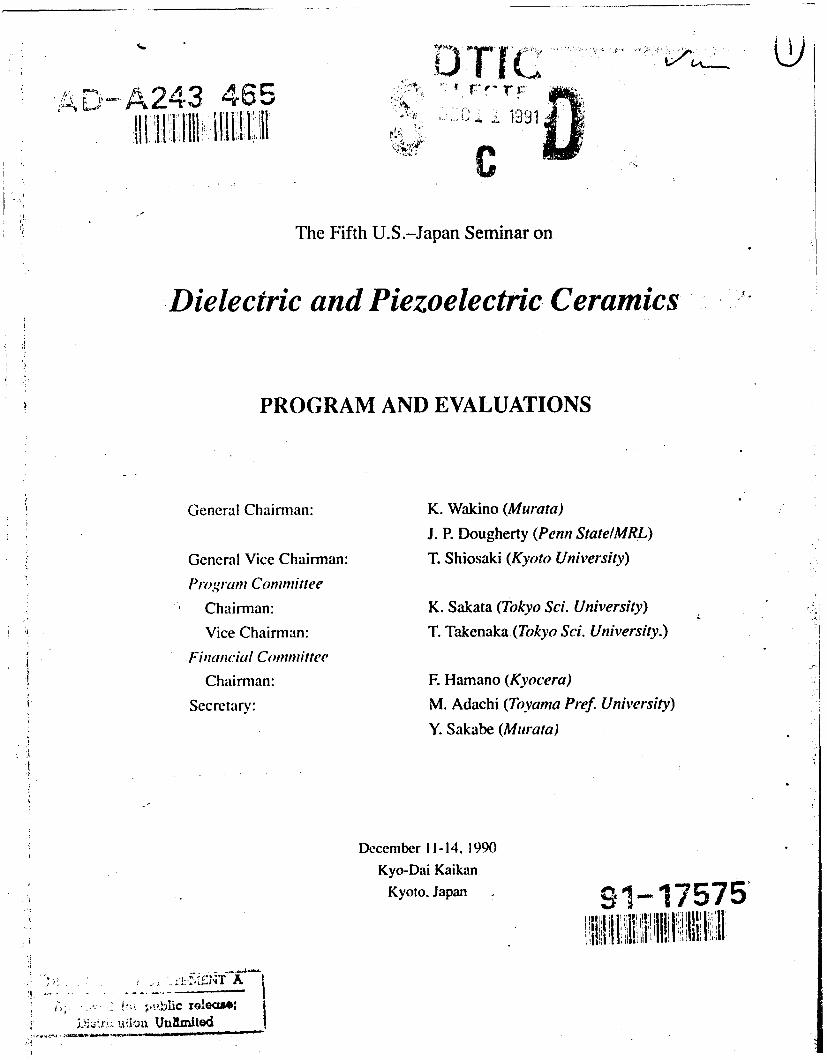
The Fifth U.S.-Japan Seminar on
Dielectric and Piezoelectric Ceramics
PROGRAM AND EVALUATIONS
General Chairman: K. Wakino (Murata)
J. P. Dougherty (Penn State/MRL)
General Vice Chairman: T. Shiosaki (Kyoto University)
Program Committee
Chairman: K. Sakata (Tokyo Sci. University)
Vice Chairman: T. Takenaka (Tokyo Sci. University.)
Financial Committee
Chairman: F. Hamano (Kyocera)
Secretary: M. Adachi (Toyama Pref. University)
Y. Sakabe (Murata)
December 11-14. 1990
Kyo-Dai Kaikan
Kyoto. Japan 91-17575
.i tblic roleaw;* '~udo.i Unlln-ted
ltl -

TABLE OF CONTENTS
U.S. Chairman's Report .............................................................................. 3
Abstract ......................................................................................... 3
Participants ..................................................................................... 3Technology Emphasis ........................................................................ 4
Poll of Japanese Interests ..................................................................... 5
Program and Abstracts ................................................................................. 7
Schedule Table ................................................................................. 8Program ..................................................................................... 9
~ ~Evaluations ............................................... 15
Dr. Thomas R. Shrout ............................................................... 16
Dr. Donald M. Smyth .............................................................. 22
Dr. Ahmad Safari ..................................................................... 30
Dr. Walter A. Schulze .............................................................. 37
Dr. B.A. Auld ........................................................................ 44
Dr. Gene Haertling ............................................................... 46
Dr. Paul Schuele .................................................................... 51
Dr. J.F. Scott ........................................................................ 52
Dr. Martin P. Harmer ............................................................... 54
List of U.S. Participants .............................................................................. 55
Report Document Page ............................................................................... 61Ace o2a Yor
! IC TtUB 0.Janouneed
Just I.:1 at io i
Distributtao/Av~llabt.llty CodeG
; Avil and/orDI t I Special
.g % \J ___

This work relates to Department of Navy Grant N00014-90-J-1928 issued by the Office of
Naval Research. The United States Government has a royalty-free license throughout the world in
all copyrightable material contained herein.
2

U.S. Chairman's Report
Abstract
The Fifth US-Japan Workshop on Dielectric and Piezoelectric Materials was held in Kyoto,
Japan on December 11-14, 1990. The local organization was from Kyoto University and Murata
Corp. U.S. organization was from the Materials Research Lab, Penn State University. There
were 123 participants: 84 Japanese and 39 U.S.; 67% of the Japanese were from industry, while
38% were from U.S. industry (up 5% from the last workshop in Japan).
The technical topics most discussed were: (1) thin film ferroelectrics and dielectrics, (2)
relaxor ferroelectrics, and (3) piezoelectric materials and processing. Barium titanate materials for
multilayer capacitors received little attention. There were no USA papers on microwave dielectrics
and no Japanese papers on single crystals.
There were no USA papers on piezoelectric devices, while many Japanese papers were
device related.
Dielectric materials for electronic packaging were few from both sides.
Participants
During the organization of this U.S.-Japan Seminar, we tried to increase the number of
U.S. industry participants. With an aggressive telephone lobbying campaign, I was able to
increase the U.S. industry participation in the workshop to 38% of the attendees. This increase
was noted in several of the evaluations. However, comments by Gene Haerding (Clemson) and
Jim Scott (Colorado) cited the even greater Japanese industry participation. The breakdown is
given in Table 1.
It should be noted that in the organizing phase that I had only 1/3 of the companies that I
contacted send participants. In contrast, the Japanese organizers turned away nearly as many
companies as they allowed to participate!
(A listing of the workshop participants follows the evaluations.)
3

TABLE 1
Participants5th U.S.-Japan Seminar
onDielectric and Piezoelectric Ceramics
U.S.A. JAPAN TOTAL
University 18 26 44
Industry 15 56 71
Government 2 8
Total 39 84. 123
Technology Emphasis
I have shown in Table 2 a classification matrix to help identify the technologies being
emphasized. From Table 2 the significance of processing and properties is apparent; Tom Shrout
(Penn State) wrote a very lucid evaluation of the processing work. This emphasis illustrates the
strong Japanese commitment to materials research in ceramics. (A part of this emphasis is also due
to the materials research backgrounds of many of the workshop organizers.)
4

TABLE 2
Paper Classifications
USA/Japan Processing Modeling Devices Reliability Total& Properties ,,
Crystals 2/0 1/0 3/0
Piezo 3/6 2/1 0/3 2/2 7/12
Relaxors 2/9 1/0 0/2 3/11
High K 3/5 1/0 4/5
MLC 1/3 0/0 4/3 5/6
Thin Films 6/13 1/1 1/0 8/14
Low K 1/4 1/0 1/1 3/5
Varistor PTC 0/5 0/1 0/6Pyro & Misc.
18/45 4/1 3/8 8/5 33/59Totals 63 5 11 13 92
Packaging dielectric ceramic material, was just barely mentioned in spite of its importance.
Of particular note was the fact that work on low temperature ceramic cofire multichip modules werenot presented in proportion to the amount of work I personally know is being done. This mightmean that commercialization is in progress and both sides have to keep quiet.
Also of note was that there were no U.S. papers on microwave materials. (I wouldrecommend that purchasing agents for these materials program dollar to yen conversions into theirbusiness calculators.)
Poll of Japanese InterestsFor the first time at a U.S.: Japan Dielectric Workshop, we asked the Japanese participants
to write down their assessments. Table 3 shows the form that was used.
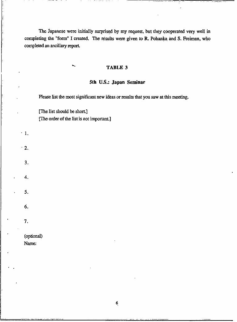
The Japanese were initially surprised by my request, but they cooperated very well in-
completing the "form" I created. The results were given to R. Pohanka and S. Freiman, who
completed an ancillary report.
TABLE 3
5th U.S.: Japan Seminar
Please list the most significant new ideas or results that you saw at this meeting.
[The list should be short.]
[The order of the list is not important.]
1.
2.
3.
4.
5.
6.
7.
(optional)
Name:
6

The Fifth U.S.-Japan Seminar on
Dielectric and Piezoelectric Ceramics
PROGRAM and ABSTRACTS
General Chairman: K.Wakino (Murata)
J. P. Dougherty (MRL/PSU)General Vice Chairman: T. Shiosaki (Kyoto Univ.)Program Committee:
Chairman: K.Sakata (Tokyo Sci. Univ.)Vice Chairman: T. Takenaka (Tokyo Sci. Univ.)
Financial Committee*Chairman: F. Hamano (Kyocera)
Secretary: M. Adachi (Toyama Pref. Univ.)
Y. Sakabe (Murata)
December 11-14, 1990
Kyo-Dai KaikanKyoto, Japan
7

Schedule Table
Morning Afternoon Evening
15:00 18:00-21:00
ReceptionDec. 11 (Tue) Registration cepion
Cocktail Parry
(CO-OP INN) (CO-OP INN)
9:00Registration 13:30-17:00 17:30
9:30-10:00
Dec.12 (Wed) Opening Remarks Poster Session I Bus Tour10:00-12:00
Overviews
(Kyo-Dai Kaikan) (Kyo-Dai Kaikan) (Kyoto City)
9:15-12:30 13:30-17:00 19:00
PartyDec.13 (Thu) Poster Session II Poster Session III Party
(Courtesy.of
DuPont Japan)
(Kyo-Dai Kaikan) (Kyo-Dai Kaikan) (CO-OP INN)
9:15-12:30 12:30-14:00Ferewell Party
Dec.14 (Fri) Poster Session IV 14:00-15:00
Committee Meeting
(Kyo-Dai Kaikan) (Kyo-Dai Kaikan)
8

PROGRAM-
Wednesday Morning I Dec. 12
9:30- 10:00 Opening Remarks
K. Wakino (Murata Mfg. Co., Ltd.)J. P. Dougherty (Pennsylvania State University)
10:00-12:00 Overviews
Chairman T. Shiosaki (Kyoto University)S. K..Dey (Arizona State University)
Plenary Lecture
P- 1 "Physics and Engineering of Ferroelectric Memories."
J. F. Scott (University of Colorado)P-2 "Chemical Processing of Electronics Ceramics."
S. Hirano (Nagoya University)
Wednesday Afternoon I Dec. 12
13:30-17:00 Poster Session I:Dielectric Ceramics and Applications (23)
Chairman I. Bum (E. I. du Pont de Nemours & Co., Inc.)N. Ichinose (Waseda University)
I-1 "Phase Distribution and Dielectric Properties of Lead Magnesium Niobate-Pyrochlore DiphasicMixtures" J. Chen and M. P. Harmer (Lehigh University)
1-2 "La-Pb Partition between Perovskite and Pyrochlore Phases"T. Yamaguchi and M. Saitoh (Research & Developement Center, Mitsubishi Mining & Cement Co., Ltd.)
1-3 "The Glassy Nature of Relaxor Ferroelectrics"LE.Cross, D.Viehland, SJang and M.Wutfing (Pennsylvania State University)
1-4 "Interaction between Relaxor and Glass in the Low-Temperature Fireable Ceramics"K. Onda, S. Ohtomo and S. Nishigaki (Narumi China Co.)
1-5 "MLC's with Copper Electrodes for High Frequency Applications"l, Bum and W. C. Porter (Du Pont Electronics)
1-6 "Multilayer Ceramic Capacitor with Ni Electrodes"H. Chono, H. Kishi and N. Yamaoka (Taiyo Yuden Co., Ltd.)
1-7 "A Study on the Degradation of Ni Electrode Ceramic Chip Capacitors"T. Nomura, S. Sumita, Y. Nakano and K. Nishiyama (Materials Research Center, TDK Co.)
1-8 "Y5V Capacitor Based on Hydrothermally Prepared Barium Titanate Zirconate Solid SolutionPowder" T. ShikidaK. Hidak, K. Fukai, M. Aoki and K. Abe (Sakai Chemical IndustryCo., Ltd.)
1-9 "Lead Perovskite Relaxor based Low Loss Ceramic Dielectric for High Voltage CeramicCapacitors" 0. Furukawa, Y. Yamashita and M. Harata (Research and Development Center, Toshiba Co.)
9

1-10 "Y5U Multilayer Ceramic Capacitors with High Specific Capacitance"T. Moi, A. Ochi, M. Nakanishi, K. Utsumi, S. Abe* and T. Yoshimoto (NEC Co., *Nippon Soda Co., Ltd.)
I-11 "Dielectric Properties of (Pbl.x,Bax)(Mgl/3Nb2/3)l-yTiyO3 Ceramics"S. Tanaka, Y. Matsushita, K. Maeda and K.Takahashi (Hitachi Res. Lab., Hitachi Ltd.)
1-12 "Chemical and Physical Effects on the Aging of FMN Relaxor Materials"M. S. Chu and J. E. Carminati (TAM Ceramics Inc.)
1-13 "Microstructure and Dielectric Properties of Lead-Based MLC Fabricated by AlternativeLamination of 2 Kinds of Dielectric Layers"
lJgarashi, S. Tashiro and Y. Mizukami (The National Defense Academy)1-14 "Oxidation and Reduction of Pd in the Presence of Ag"
J. P. DoughrtyS- F.Wang and W.Huebner (Materials Research Laboratory, Pennsylvania State University)
-15 "Unusual Dielectric Anomalies in (Pb,La)TiO3 Ceramics"M.Kuwab , K. Goda and K. Oshima (Kyushu Institute of Technology)
1-16 "Influence of Chemisorbed Oxygen to the PTCR and VDR Effects in Perovskite Pceramics"N. Ichinose, Y. Nakano and T. Takahashi (Waseda University)
1-17 "Microstructure of High-Purity, Fast-Fired, Near-Stoichiometric Barium Titanate"
W. A. Schulze and R.C.VanAlstine (New York State College of Ceramics)1-18 "A Study on Non-Oxide Ceramics for Electronic High-Performance Applications"
H. Nakabara, C. H. Pai, K. Koumoto and H. Yanagida (University of Tokyo)
1-19 "SiC as a Dielectric Ceramic" G.R.lov and T.K.Gupta (Alcoa Technical Center)1-20 "Dielectric Properties of Nonstoichiometric Barium Zinc Niobium Tantalate Ceramics"
H- Ohuchi (Shonan Institute of Technology)1-21 "Dielectric Properties and Micro-Structure of (SrCa)3Ti2O7 Ceramics"
A. Ymada, T. Honda, Y. Utsumi and H. Watarai (Mitsubishi Electric Co.)1-22 "Microwave Characteristics of BaO-TiO2-Rare Earth Oxide Ceramics"
E. Fukuda, A. Takasugi, M. Fujinaga and R. Kitoh (Ube Industries Ltd.)1-23 "Third Harmonic Distortion of Dielectric Resonator Materials"
K. Wakino, Y. Ishikawa, T. Nishikawa and H. Tamura (Murata Mfg. Co., Ltd.)
Thursday Morning / Dec. 13
9:15-12:30 Poster Session II:Reliability of MLC's, Substrates and Semiconductors (12)
Chairman A. S. Bhalla (Penn State University.)Y. Sakabe (Murata Mfg. Co., Ltd.)
11-1 "Surge Test Characteristics of High K Multilayer Ceramic Capacitors"H. C.Ling and D. D. Chang (AT & T Bell Laboratories)
11-2 "Use of Highly Accelerated Life Test (HALT) to Determine Reliability of Multilayer CeramicCapacitors" JP. Canner and R. J. Confer (Murata Erie N. A., Inc.)
11-3 "Accelerated Life Tests of Multilayer Ceramic Capacit3rs with Thin Dielectric Layers".. H.JMahe , T. I. Prokopowicz and G. A. Shim (MRA Laboratories Inc.)
10

11-4 "Role of Minor Phase Additions on Aging and Dielectric Stability Characteristics in-BaTiO3"L.C..Buchaan T.R.Armstrong and R.D.Roseman (University of Illinois)
11-5 "Acoustically Aided Board Flexure Testing of Surface Mount Capacitors"K. Ritchie. C. Nies and T. Rutt (AVX Corp.)
11-6 "Control of Mass Transport and the Attendant Point Defects - The Next Generation-of Reliabilityin Dielectrics" N.Q. Eror (University of Pittsburgh)
11-7 "Cordierite Glass-Ceramic Substrate for IBM's Mainframe Computers" R.R.Tummala (IBM)11-8 "The Reaction between AIN Ceramics and Ti Film after High Temperature Treatment"
T..Xsummt, K. Yamakawa, N. Iwase and N. Shinozawa* (R & D Center, *New Materials EngineeringLab., Toshiba Co.)
11-9 "Interaction between Glass and CaTiO3 Ceramics" T. Yamguhi and H. Ayaki (Keio University)II-10 "Interfaces of Electronic Ceramics / Electrodes and Wetting Properties"
S.Sugihara and K. Okazaki (Shonan Institute of Technology)II-11 "Formation Mechanism of Potential Barrier of ZnO Varistor" i-hirasaki, J. Tanaka, H. Haneda,
S. Ijishita and K. Sato (National Institute for Research in Inorganic Materials)11-12 "Relationship between Degradation Phenomenon and Trap Levels in ZnO Varistor"
M.i TakatY. Watanabe, K. Nakajima and S. Shichino (Nagaoka University of Technology)11-13 "Fabrication of Jointed Type PTC Ceramics with Different Composition and Their Evaluation"
T. Ymamoto, S. Ohashi and S. Tomono (National Defense Academy)
Processing (11)
Chairman T. Yamaguchi (Keio Univ.)W. A. Schulze (New York State College of Ceramics)
11-14 "Sol-Gel Processing of Pb(Mg,Nb)0 3 Dielectrics"
K. Kiutx, W. Sakamoto and S. Hirano (Nagoya University)11-15 "Fabrication of Porous Electroceramic Structures by Reactive Calcination"
T. R. Shrout, Y. S. Kim and J.Fieldingjr (Materials Research Laboratory, Pennsylvania State University)11-16 "Mechanism of PNN Based Perovskite Ceramics Formation"
T. Yoshimoto, Y. Sasaki and A. Nagai (Odawara Research Center, Nippon Soda Co., Ltd.)11- 17 "Application of Attrition-Milling to Lead-based Relaxor' LjKai, H. Kagata and Y. Yokotani*
(Materials & Devices Res. Lab.,*Central Res. Lab., Matsushita Electric Ind. Co., Ltd.)If- 18 "Chemical Precipitation and Coating Processes for Synthesis of Next Generation Dielectric
Powders"
D.K.Sanson, S. A. Bruno, I. Bum, K. Sasaki, H.E.Bergna and PiJesson(E. I. du Pont Co., Inc.)11- 19 "Synthesis of Metal-Vetivenoxide Compounds and Its Application for Thin Films and Powders"
K. Hyashi (Research and Development Lab., Shoei Chemical Inc.)11-20 "The Growth and Characterization of Tungsten Bronze SrxBal-xNb2O6 Single Crystal Fibers"
A.. Bba1Ia and J. K. Yamamoto (Materials Research Laboratory, Pennsylvania State University)11-21 "Sol-Gel Processing of Ferroelectric Fibers" S.C. Choi*, S. 1. Aoki, M. Miyayama, D. A. Payne*
and H. Yanagida (RCAST, University of Tokyo,*Ajou University, ** University of Illinois)
ii
11-22 "Processing of Stoichiometric and Ti Doped LiNbO3 Films with Preferred Orientation fromMetal Alkoxides" S.£lHian, K. Kikuta and K. Kato (Nagoya University)
11-23 "A New Method for the Preparation of Aa+( (BIxb+,BIII.xb+)n BIIl.nc+ } 03(a+b(1-n)+cn=6) Type Solid Solutions" KKake (Faculty of Engineering, Chiba University)
11-24 "Solubility and Phase Stability of Barium Titanate in Aqueous Suspension"Jam air, Benjamin L. Utech, K. Osseo-Asare and Joseph P. Dougherty (Pennsylvania State University)
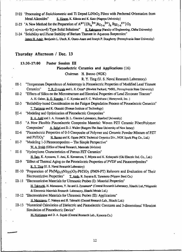
Thursday Afternoon / Dec. 13
13:30-17:00 Poster Session IIIPiezoelectric Ceramics and Applications (16)
Chairman H. Banno (NGK)R. Y. Ting (U. S. Naval Research Laboratory)
III-1 "Temperature Dependence of Anisotropy in Piezoelectric Properties of Modified Lead TitanateCeramics" T.R. GUmria and L. E. Cross* (Hewlett Packard, *MRL, Pennsylvania State University)
1-2 "Effects of Silica on the Microstructure and Electrical Properties of Lead Zirconate Titanate"A. H. Gabor, B. G. Koepke, J. C. Kyonka and F. C. Wallenhorst ( Honeywell, Inc. )
111-3 "Reliability-based Consideration on the Fatigue Degradation Process of Piezoelectric Ceramics"T.Tnimoto and K. Okazaki (Shonan Institute of Technology)
II1-4 "Modeling and Optimization of Piezoelectric Composites"
B. A. Auld and J. A. Hossack (E. L. Ginzton Laboratory, Stanford University)II1-5 "A New Flexible Piezoelectric Composite Material: Woven PZT Ceramic Fiber/Polymer
Composites" A. SaM and D. J. Waller (Rutgers-The State University of New Jersey)111-6 "Piezoelectric Properties of 0-3 Composite of Polymer and Ceramic Powder Mixture of PZT
and PbTiO3" H. Banno and K. Ogura (NTK Technical Ceramics Div., NGK Spark Plug Co., Ltd.)II-7 "Modeling 1-3 Piezocomposites -- The Simple Perspective"
W. A. Smith (Office of Naval Research, Materials Division)I1-8 "Hydrophone Characteristics of Porous PZT Ceramics"
H. Sato, K. Ayusawa, T. Arai, K. Kawamura, T. Miyata and K. Kobayashi (Old Electric Ind. Co., Ltd.)II-9 "Effect of Thermal Aging on the Piezoelectric Properties of PVDF and Piezocomposites"
R. Y. Ting (U. S. Naval Research Laboratory)1-10 "Preparation of Pb(Mgl/3Nb2/3)03-PbTiO3 (PMN-PT) Relaxors and Evaluation of Their
Electrostrictive Properties" T..And, R. Suyama K. Tanemoto (Nippon Steel Co.)I11-11 "Electrostrictive Materials for Ultrasonic Probes (I): Material Properties"
H. akeuci, H. Masuzawa, Y. Ito and S. Jyoumura* (Central Research Laboratory, Hitachi Ltd.,*Magnetic& Electronic Materials Research Laboratory, Hitachi Metals Ltd.)
111-12 "Electrostrictive Materials for Ultrasonic Probes (II): Applications"H. Masuzawa, C. Nakaya and H. Takeuchi (Central Research Lab., Hitachi Ltd.)
111-13 "Numerical Calculation of Dielectric and Piezoelectric Constants and 3-dimensional VibrationSimulation of Piezoelectric Device"
A NiShimua and D. A. Sagala (Central Research Lab., Kyocera Co.)
12

11-14 "Phase Relations in the (Bi 0 .5Na 0 .5)TiO3 -PbTiO 3 Solid Solution Ceramics and ItsPiezoelectric Properties" LSaka , T. Takenaka and Y. Naitou (Science University of Tokyo)
I1-15 "A High Sensitivity IR Detector Using Modified PZT Ceramics"
J. Liin and T. Shiosaki (Faculty of Engineering, Kyoto University)
1I-16 "Effects of Partial Oxygen Pressure During Heat Treatment of Multilayer PZT Ceramics"
MKalm (Naval Research Laboratory)
Actuator, Mechanical Properties (7)
Chairman S. W. Freiman (NIST)H. Igarashi (National Defense Academy)
111-17 "A Piezoelectric-Ceramic Hollow-Cylinder Torsional Vibrator"H. Shimizu and T. Yoshida* (University of Electro-Communications, *Tokin Corporation)
111-18 "Auto-Focusing System Utilizing Electrostrictive Actuators"R. Suyama, K. Tanemoto, Y. Kobayashi* and M. Yajima* (Nippon Steel Co., *Sankyo Seiki Mfg.)
I1-19 "A Small-Size Ultrasonic Linear Motor" Jloda and K. Murano (Sony Corporate Research Lab.)
111-20 "Piezoelectric Actuator Properties of Pb(Znl/3Nb2/3)O3-KNbO3-PZT Ceramics"T.aken, M. Satou and K. Sakata (Science University of Tokyo)
111-21 "A Quantitative Theory of Microstructure in Polycrystalline Ceramics: Application toCalculation of the Effective Elastic Constants and Internal Stresses"
S. K. Kurtz, S. Kumar, J. R. Banavar K. Kunz, D. Steich, S. S. Chang, M. Leffler and M. Cieplak*(Penn State University, *Polish Academy of Science)
I1"-22 "Effects of Poling on the Mechanical Properties of Piezoelectric Ceramics"H. Ymaoka and Y. Ushida (Mitsui Petrochemical Industries)/
111-23 "Fracture Behavior of Cyclically Loaded Lead-Zirconate-Titanate (PZT)"G. S. White, A. S. Raynes and S. W. Freiman (National Institute of Standards and Technology)
Friday Morning/ Dec. 14
9:15- 12:30 Poster Session IV:Dielectric and Ferroelectric Thin Films, Electrooptics (21)
Chahrman I. Ueda (Matsushita Electric Industrial Co.)
R. R. Neurgaonkar (Rockwell Science Center)IV-1 "Electrical Degradation Mechanisms in Ferroelectric Thin Film Memories"
D. M. Smyth (Lehigh University)IV-2 "Ta2O5 Thin-Film Capacitor for Ultra High Frequencies"
S. Yamanaka and H. Yoshino (Sumitomo Electric Industries, Ltd.)IV-3 "Electrical Characterization of Ferroelectric Thin-Film Capacitors"
P. J. Schuel and S. D. Traynor (Ramtron Co.)
13

IV-4 "Advances in Perovskite Thin-Films: Chemical Processing, Properties, and ElectricalApplications" SK.x (Arizona State University)
IV-5 "Preparation of PbTiO3-La2O 3 System Thin Films by Sol-Gel Processing".Qkamia, H. Nagata, M. Watanabe, N.Sakai and H.Yamamura (Tosoh Corporation)
IV-6 "Preparation of PbxMl-xTiO3 (M= Sr, Ba) Thin Films by the Thermal Decomposition ofOrganometallic Compounds"K. Saegusa, M. Sasaki and K. Yamada (Tsukuba Research Lab., Sumitomo Chemical Co.)
IV-7 "Synthesis of SrTi 3 and CaTiO3 Thin Films by Hydrothermal Electrochemical Method"Y. Sakabe, Y. Hamaji, M. Hayashi. Y. Ogino, N. Ishizawa* and M. Yoshimura* (Murata Mfg. Co., Ltd.,*Research Laboratory of Engineering Materials, Tokyo Insititute of Technology)
IV-8 "Effect of Pulsed Laser Irradiation in Preparation of Pb(Zr0.52Ti0.48)O3 Films by LaserAblation" T. Minamikawa, Y. Yonezawa, K. Segawa, A. Morimoto*, T. Shimizu*, S. Otsubo"*,
H. Kidoh*** and T. Ogawa*** (Industrial Research Institute of Ishikawa, *Kanazawa University,**Shibuya Co., Ltd., ***Murata Mfg. Co., Ltd.)
IV-9 "Thin Film Growth of PbTiO3 by Photo-MOCVD"
M. Shimizu, T. Katayama and T. Shiosaki (Faculty of Engineering, Kyoto University)IV-10 "PbTiO 3 Thin Films by Chemical Beam Deposition"
A. 1. Kingon, K.Y.Hsieh, L. L. H. King and S-H. Rou (North Carolina State University)IV-11 "Preparation and Dielectric Properties of Ferroelectric PbTiZrO3, BaTiO3 and SrTiO3"
1. Ueda, K. lijima and K. Kugimiya (Central Res. Lab., Matsushita Electric Industrial Co., Ltd.)IV-12 "PbTiO3 Thin Film Growth by Multi-Metal Target Sputtering"
K. Tergo, S.P.Leiphart* and S. B. Krupanidhi* (Sumitomo Metal Industries, Ltd., *Penn State University)IV-13 "Pb(Zr,Ti)0 3 and KNbO3 Thin Films by Ion Beam Sputter Deposition"
A. I. Kingon, T.M.Graettinger, S-H. Rou, H. N. Al-Shareef, K. D. Gifford, P. D. Hren, M. S. Ameen and0. H. Auciello* (North Carolina State University, *Also Microelectronics Center of North Carolina)
IV-14 "Polar Axis Oriented Ferroelectric Pb(Zr0.gTi0.1)O3 Film by Sputtering"1Shiosaki and T. Okamura* (Faculty of Engineering, Kyoto University, *Kyocera Corporation)
IV-15 "Preparation of C-Axis Oriented AIN Thin Films by Low-Temperature Reactive Sputtering"H Okn, K. Shibata and S. Nakano (Functional Materials Res. Center, Sanyo Electric Co., Ltd.)
IV-16 "Properties of Bi4Ti30l 2 films by ECR Plasma Sputtering Deposition" Y. Masuda, A. Baba,H. Masumoto*, T. Goto*, M. Minakata** and T. Hirai* (Hachinohe Institute of Technology, *Institute forMaterial ResearchTohoku University, **Institute of Electrical Communication of Tohoku University)
AV-17 "Linear and Nonlinear Optical Properties of Tungsten Bronze Crystals"
-R, R.. ergaonk, W.K.Cory, J. R. Oliver and Edward3. Sharp* (Rockwell International Science Center,*Center for Night Vision and Electro-Optics)
IV-18 "Tungsten Bronze Crystals for Photorefractive Applications"LLDu~aua (DARPA DSO)
IV-19 "Selected Properties of Acetate-Derived PLZT Thin/Thick Films"-iJunlin (Clermson University)
IV-20 "Properties of Electro-Optic PLZT Ceramics Fabricated by Partial Coprecipitation Method"LNaga , T. Kiyota* and M. Furuno* (The National Defense Academy, *Tamura Corporation)
IV-21 "Excimer Laser Ablated PZT Films"S. B. Kmpanidhi, D. Roy and J.P.Dougherty (Materials Research Laboratory)
14

EVALUATIONS
Dr. Thomas R. ShroutMaterials Research Laboratory
Penn State University
Dr. Donald M. SmythMaterials Research Center
Lehigh University
Dr. Ahmad SafariDept. of Ceramic Science & Engineering
Rutgers University
Dr. Walter A. SchulzeNew York State College of Ceramics
Alfred University
Dr. B.A. AuldEdward L. Gintzon Laboratory
Stanford University
Dr. Gene HaertlingClemson University
Dr. Paul SchueleRamtron Corporation
Dr. J.F. ScottCondensed Matter Laboratory
University of Colorado at Boulder
Dr. Martin HarmerMaterials Science and Engineering
Lehigh University
15

U.S.:JAPAN SEMINAR ON DIELECTRIC AND PIEZOELECTRIC CERAMICS
December 11-14, 1990Kyoto University
Kyoto, Japan
Thomas R. ShroutPennsylvania State UniversityMaterials Research Laboratory
University Park, PA 16802
BACKGROUND
In addition to the conference in Kyoto, universities and companies visited in Japan includedthe following:
* Shonan Institute of Technology, Fujisawa* Nippon Soda, Odawara* NEC/R&D, Kawasaki* Toshiba/R&D, Kawasaki• Marcon Electronics, Nagai
Along with representatives from the above, Japanese participants at the U.S.:Japan meetingincluded affiliates from numerous Universities* (- 15) and industrial companies (- 24). This is inreverse contrast to the U.S. participants at the seminar, 23 and 16 for universities and industry,respectively.
RESEARCH TOPICS (DIRECTIONS)
The topic areas presented below have been broken down into material families and whetherin bulk or thin film form.
RelaxorsIn the area of relaxor ferroelectrics a considerable amount of effort in R&D is being
performed. From Table I, the fundamental work is being performed at U.S. universities (namelyPenn State) whereas the work in Japan is primarily related to processing and applications such asMLCs and actuators. Much of the processing is performed at chemical companies, e.g., NipponSoda, Mitsubishi Materials, Narumi China, as well as large MLC related companies, NEC,Toshiba, Marcon, Matsushita, etc. Processing work was related to optimum mixing, etc., usingstate-of-the-art milling (attrition) and wet-chemical (alkoxide) methods. Also, much of the workon relaxors was in reality redundant in that the formulations studied are obviously selected on thepremise to avoid patent infringement. It is interesting to point out that now 6?>4LC manufacturers,including multilayer actuators, are currently in production of relaxor-based materials.
* Encompassed with universities are government and related R&D facilities.
16

TABLE I
Materials, # of Papers as Related to U.S. and Japan Interests
BULK THIN FILM
Topics U.S. Japan U.S. Japan
Relaxor Ferroelectrics 3 [F,P] 14 [P,A] 1
BaTiO3 and Related 10 [F,P,A] 2 [F,P,A] 1
PZT/PT and Related 10 [F,P,A] 14 [I,F,P,A] 8 6
Sensors (PTCR/Varistors) 3 [I,F,P]
Microwave 4 1
Packaging 2 [A] 1-2 [I,P]
Tungsten Bronze and Cryst:-si 2 [F,A] 1 [P] ---
Miscellaneous (LiNbO3) 1 (Ta205) 1 [I,P]
Reliability 3 [F]
General [F]
(TiNTiO2) 4d Bismuth Tit nate 1
I-Innovative; F-Fundamental; P-Processing; A-Applications
They are in order of chronological implementation:
* TDK • Marcon (Toshiba)• NEC * Murata• Mitsubishi Materials • Nippon Soda (powder manufacturing only)
Generally, the relaxor formulations are based on PMN. The market is reportedly about thesame as Ni-electroded MLCs and only includes large capacitance parts (> 10 tf).
To date, little has been reported on reliability of relaxors, though the Japanese are snngiyinterested in this area. They feel reliability is the key to success and not performance.
Only a minimal amount of work in relaxor thin films has been reported. They appear to begood for capacitor type devices and perhaps electrostrictive micro-motors.
17

BaTiO3 and Related Materials
A considerable amount of work on BaTiO3 and related materials comes from the U.S.Fundamentally, electrode interfaces and defect chemistry is being examined at both universities andindustries. Perhaps, the best work comes in processing. DuPont utilizes a chemical precipitationand coating process to minimize the level of required fluxes/additives, resulting in enhanceddielectric behavior and overall performance.
In Japan, very good fundamental work on electrode "wetting" comes from the ShonanInstitute of Technology. Processing: the Sakai Chemical Company's hydrothermally derivedmaterial is attractive and commercially available.
Packaging
Interestingly, the papers from U.S. companies (no universities) were applied presentingnew SiC (ALCOA) and established cordierite-glass (low K-IBM) substrate materials. Work inJapan is heavy on AIN (high thermal conductivity) with Sony doing AIN thin films by reactivesputtering. Jnterface A1N/i studies are being done at Toshiba.
Microwave Dielectrics
. work was reported by U.S. participants with most of the research being reported byJapanese industries, Murata, Mitsubishi, and UBE. Nothing significant was reported.
Sensors (PTCR/Varistors)Good fundamental work on ZnO varistors and P71'CR ceramics came from the Japanese
universities of the Nagaoka University and Tsukuba (Science) City (ZnO)-defect chemistry.Again, no U.S. participants presented work in these ,reas. Though varistors represent asignificant market in Japan and the U.S., no R&D from associated industries was reported.
Thin Films
Perhaps the best work in PZTs comes in the area of thin films. The U.S. and Japan arequite active in this area. Both have developed state-of-the-art techniques with emphasis on grainorientation. Excellent work comes from Colorado, Ramtron, Penn State, N.C. State, and Arizona,
More work, however, in the area of domain theory, stress effects, interface effects, is stillneeded. This is especially true in Japan where lesz fundamental work has been done. Thin filmsis probably the only area where I feel the Japanese are behind the U.S. in development.
Thin Films (Miscellaneous)
In terms of practical importance, the Ta2Q.5 thin film work by Sumitoma Industries maysurpass any potential for using perovskites particularly for high speed decoupling capacitors wherehigh capacitances are not required.
In thin films, the novel hydrothermal method performed by Murata is very interesting forboth capacitors and perhaps varistors.
18

PZT/PT-Piezos/Pyros
The U.S. and Japan are quite active in the area of PZT and PT related materials. However,most of the work p'esented by U.S. participants was outdatturedunR nt andnot significant. Theprocessing of PZT fibers may have some merit. In Japan much of the same is true. Some goodwork in mechanical properties comes from the Defense Academy. Kyocera's transducer modelingby finite element analysis was also of importance.
In terms of piezo composites, good fundam.." ,, rk comes from Stanford.In applications, some new designs were i: .,.; ,[ ,c by Japanese companies, including the
cylindrical actuator from the University of Elcx_. -"."os ', .wation and Tokin and linear motors bySony.
New non-Pb-based piezoelectrics developed at the Science University of Tokyo appearinteresting, but the argument that they are non-PbO . e. '.,&'ce, non-toxic, is totally a misconcept,since bismuth is in the same EPA class as PbO,
Fabrication of very large optically transpax-Mt PLZT ,sing tape casting and optimumchemically derived powders was a fine piece of work from the Japanese Defense Academy.
Miscellaneous
The paper by Kurtz, et al. (Penn State) on ceraoic simulation was fundamental and ofsignificant importance for the understanding of elastic behavior in polycrystalline materials.
SUMMARY OF MEETING
• Little innovative or breakthrough science was piesented.• U.S. more fundamental than Japan (universities only).• Japan--exceilent in process.r g to insure reliability. Applied R&D at both the university
and industrial level.Most promising Japanese university-Shonon Institute, a recently founded MRL forelectronic ceramics. Most universities have insufficient staffs to be affective. This includesthe U.S. universities.
* U.S. is ahead in thin films, particularly in the fundamental understanding.• Japan good at developing devices, e.g., piezo motors, actuators.• Much of what was presented was redundant and old. Perhaps, industrial people cannot
present up to date work. This is no excuse for university representatives.Meeting had excellent U.S.:Japan interaction.
Shonan Institute of Technology
Newly found MRL for electronic ceramics. Have university:industry meetings every twomonths. More than 50 industrial companies and other institutes are invited.Topics Include:
• Mechanical properties of composites including ferroelectrics.0 Metal-glass-ceramic interactions.* Crystal growth.
19

• HIP and HUP.• RF sputtering of films.* Plezo composites for hydrophones.* Nano heterocoagulation/ceramic processing.• Surface characterization (ESCA).* Defect chemistry of electronic ceramics (ZnO, PTCR).
Approximately 8-10 associate and full professors. State-of-the-art processing,characterization, testiog, etc. equipment. This institute will be a strong force in electroric ceramicsin Japan. Conceptually, U.S. universities need a certain size of disciplinary effort to performinnovative and high qmlity research.
Nippon Soda
A chemical company who diversified in the manufacturing of elec- o-ceramic powders,namely relaxors.
9 Chemical method using alkoxides as well as state-of-the-art chemical processingequipment.
* No U.S. company making relaxors by chemical methods.(?)• The powder is not fundamentally superior, nor highly advanced. However, the powder
meets the Japanese requirement of obtaining high reliability.* Approximately 2-3 man years of effort.9 Strong collaboration with NEC.
NEC (R&D)
Topics:* MLCs 5 Relaxors0 Actuators
Packaging (AIN), Glass-Cordierite (low K)Artificial Superstructures
* 10-12 man years.State-of-the-an characterization and prncessing equipment.Was not shown any manufacturing facilities.
Toshiba (24 Billion Dollar Company)Over the last ten years the % of gross sales expended for R&D went from 6 -+ 8% and is
expected to go to 10%.Electro-Ceramic Topics:
"Functional ceramics." Note: The term used in Japan for high tech ceramics.
* Packaging (AIN, hybrids).
20

* Piezo transducers for bio-medical applications.* MLCs.• ZnO varistors.• Thin film capacitors (PMN-based).
No breakthroughs, but extremely high reliability. Will only invest in "large" volumecomponents due to large capital investment costs. Perhaps only - 10-12 man years of effort.
Key to success is: 1) large % investment to R&D and 2) long term planning-5+ years.
Marcon ElectronicsCapacitor company (Al, tantalum, MLCs, and varistors). Very open, was shown complete
production line of relaxor MLCs and ZnO varistors including multilayer varistors.
• Relaxor MLCs > 10 pgf.• Goal is to replace tantalum capacitors with MLCs.• Use automated state-of-the-art, processing "no problem with Pb containing materials."• All equipment commercially available.
- clean rooms- attrition mills and mixing- tape casters, etc.
NEW TOPIC AREAS
In summary of my trip to Japan, R&D areas needed for U.S. universities and industry arepresented in the following:
R&D Areas NeededUniversity* Surface chemistry/powder processing/nano-heterocoagllation and characterization (ESCA).• Reliability of relaxors.• Mechanical properties of relaxors and related dielectrics.• Domain theory, interface analysis and modeling of thin films.• New thin film approaches, e.g., hydrothermal.• New thin film materials, e.g., Ta2O5.. Need long term funding (> 1 year).
Lnjs* Need large capital investment to obtain state-of-tht.- mt proctss'ng equipment (not thin
films).* Need to work barder and demonstr.te dedication.
Should stress more on reliability and less on performance.• Need larger % gross R&D investment and long term planning.
21

REPORT ON FIFTH U. S.-JAPAN SEMINAR ON DIELE"CTRIC AND
PIEZOELECTRIC CERAMICS, AND ON RELATED LABORATORY VISITS
Kyoto, Japan, December 11-14, 1991
Donald M. Smyth
Materials Research Center, Bldg 5
Lehigh University
Bethlehem, PA 18015
22
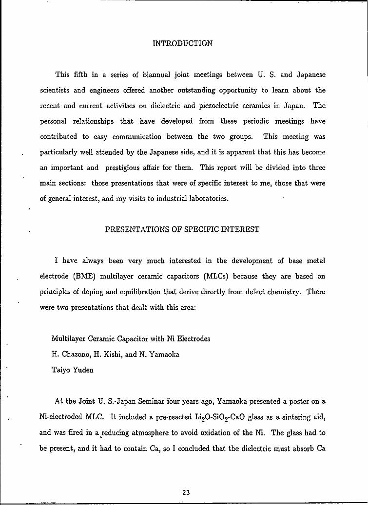
INTRODUCTION
This fifth in a series of biannual joint meetings between U. S. and Japanese
scientists and engineers offered another outstanding opportunity to learn about the
recent and current activities on dielectric and piezoelectric ceramics in Japan. The
personal relationships that have developed from these periodic meetings have
contributed to easy communication between the two groups. This meeting was
particularly well attended by the Japanese side, and it is apparent that this has become
an important and prestigious affair for them. This report will be divided into three
main sections: those presentations that were of specific interest to me, those that were
of general interest, and my visits to industrial laboratories.
PRESENTATIONS OF SPECIFIC INTEREST
I have always been very much interested in the development of base metal
electrode (BME) multilayer ceramic capacitors (MLCs) because they are based on
principles of doping and equilibration that derive directly from defect chemistry. There
were two presentations that dealt with this area:
Multilayer Ceramic Capacitor with Ni Electrodes
H. Chazono, H. Kishi, and N. Yamaoka
Taiyo Yuden
At the Joint U. S.-Japan Seminar four years ago, Yamaoka presented a poster on a
Ni-electroded MLC. It included a pre-reacted Li20-SiO 2-CaO glass as a sintering aid,
and was fired in a reducing atmosphere to avoid oxidation of the Ni. The glass had to
be present, and it had to contain Ca, so I concluded that the dielectric must absorb Ca
23

from the glass to serve as the acceptor dopant that is required to maintain an insulating
dielectric after firing in a reducing atmosphere. The system was thus closely related to
the Ca-doped composition used by Murata for their BME units.
This year, modifications were described that produced BME units that meet X7R
specifications. This seems primarily to involve the addition of around 0.5 mol% MgO
which served to depress the dielectric constant at the 1250C Curie point, giving a flatter
temperature dependence that falls within the X7R requirements. The precise
mechanism for this is not clear. Mg will also act as an acceptor dopant that can help to
maintain an insulating dielectric after firing in a reducing atmosphere. The resulting
life-test results were outstanding for a BME unit. After questioning this, it was stated
that this was a very recent laboratory result that had not yet been verified for mass-
produced units.
These capacitors are Fired at 12000C in a N2-H2 "controlled atmosphere". This is
inherently an uncontrolled system, since the oxygen activity will depend on such things
as the water content of the gas mixture. Whether or not this is controlled is not clear.
In any case, it is a very reducing atmosphere, and I cannot believe that the dielectrics
come out of it in an insulating state. Apparently to correct this, there is a subsequent
anneal at 10000C in N2 . This is also an uncontrolled situation where the oxygen activity
will depend on the accidental oxygen content of the commercial N,) gas. It app2ars that
the units are sintered to a semiconducting state and then oxidized back to an insulating
condition. The annealing step could either be a re-equilibration of the dielectric at an
oxygen activity that will still not oxidize the Ni, or it may depend on kinetic control
whereby the dielectric reoxidizes faster than the Ni oxidizes. My impression is that the
latter is the case.
24

The Taiyo Yuden people continue to be very clever in an intuitive way in
developing BME capacitors of high quality.
A Study on the Degradation of Ni Electrode Ceramic Chip Capacitors
T. Nomura, S. Sumita, Y. Nakano, and K. Nishiyama
TDK
Once again, this appears to involve firing in a highly reducing atmosphere that
gives a semiconducting dielectric tUat is restored to an insulating state by an oxidizing
anneal. The life-time under highly accelerated life-test conditions (HALT), 200 Vdc at
200"C, was measured as a function of the oxygen partial pressure during sintering, and
the temperature during annealing. The normal conditions were 1340C, 10- 12 atm, and
2 hours for sintering, and 1100*C, 10"5 atm, and 3 hours for annealing. The dielectric
composition was essentially that pioneered by Murata, an alkaline earth rich, Ca-
containing BaTi0 3 , with small amounts of MnO and SiO2 .
It was observed that the life-time under HALT conditions increased steadily as the
oxygen partial pressure during sintering was reduced from 10-5 to 10-13 (problems arose
at lower pressures because of anomalous sintering). In comparing chips sintered at 10-8
and 10-12 atm, it was noted that for the higher pressure, the "grain boundaries"
contained substantial amounts of Ca, Mn, Fe, and Ni, all acceptor impurities. These
concentrations were greatly reduced in the chips sintered at the lower pressure, and a
Mn-rich region was noted adjacent to the Ni electrodes. These results leave a lot of
questions, but it is tempting to suggest the following scenario. At the higher oxygen
pressures, the acceptors are highly soluble, and are incorporated in the dielectric. Afterthe oxidizing anneal, they are compensated by- oxygen vacancies, whose migration
25

results in short life-times. The solubilities of the acceptor impurities are suppressed at
the lower partial pressures, and they are segregated in impurity-rich layers near the
electrodes. We have observed such a suppression of the solubility of acceptor impurities
at low oxygen partial pressures, which occurs because the high oxygen vacancy
concentration that results from reduction interacts through a common-ion effect with
the vacancies that result from the acceptor content. When the solubility of the
acceptor impurities has been suppressed by highly reducing sintering conditions, they
cannot enter the lattice during the annealing step, because of very low diffusivities, so
the oxygen vacancy content of the dielectric remains low, and the life-time increases
accordingly.
It was also observed that the life-time increased as the annealing temperature was
increased from 800 to 1100°C, and then fell off again. The initial rise can probably be
attributed to increasingly complete reoxidation of the dielectric to an insulating state,
while the drop above 1100°C reflects excessive oxidation of the Ni electrode layers.
This investigation was based on some good ideas, but was not pursued in enough
detail to reach firm conclusions.
Chemical Processing of Electronic Ceramics
S. Hirano
Nagoya University
This plenary lecture by Professor Hirano was an excellent overview of processing
routes. He does consistently excellent work and is clearly a leader in this field. His
subsequent poster presentations on sol-gel processing of PMN and LiNbO 3 were also of
great interest to me.
26

OTHER PAPERS OF INTEREST
There were two papers describing the preparation of alkaline earth titanates by
hydrothermal techniques, one from Sakai Chemical Industry, and the other a joint effort
by Murata and the Tokyo Institute of Technology. This is an interesting new approach
that we are hearing more and more about, primarily from Japan. The Sakai poster
described the preparation of a very fine-grained powder, while the Murata team used an
electrochemical technique to form thin films on a Ti anode.
Because of our intensive study of Ba zinc niobate, I was particularly interested in
two papers on related materials. A paper from Toshiba described a Pb zinc niobate
(PZN) dielectric for low-loss, high voltage applications. The microwave properties of
BZN with partial replacement of Nb by Ta was studied as a function of compositional
variables in a paper from Shonan Institute of Technology.
LABORATORY VISITS
Murata Manufacturing Company
On December 10, I visited the Research Laboratories of Murata for discussions with
Drs. Sakabe and Wakino, and to give a seminar on ionic transport in ferroelectrics.
Their production of Ni electroded multilayer capacitors continues to grow and is now
approaching 200,000,000 per month, approximately ten times their production rate at
the time of my last visit in 1986. They have explored two different approaches for
BME capacitors: a low-fired composition with Cu electrodes, and the acceptor(Ca)-
doped composition that can be fired in a reducing atmosphere with Ni electrodes. They
have concluded that the latter is the best approach and have abandoned the low-fired,
27

Cu-electroded system. As stated above, it appears to me that they are now firing under
reducing conditions that give a semiconducting dielectric, and are then restoring the
insulation resistance by means of an oxidizing anneal. This differs from the original
approach in which they fired the capacitors within a very narrow window of oxygen
partial pressures that would not oxidize the Ni but would still give an insulating
dielectric. The acceptor doping moved the insulating state below the oxygen activity of
the Ni/NiO equilibrium. It was subsequently found that an additional oxidizing anneal
relieved a problem with the hot leakage current. This anneal has to oxidize the
dielectric without oxidizing the Ni, and the process then becomes kinetically controlled.
Once this step was added, there is less reason to try to keep the dielectric insulating
before the anneal. The acceptor dovant may now be serving to increase the rate of
oxidation of the dielectric by enhancing the oxygen vacancy content.
It was also indicated that there had been problems with life-test stability which
does not surprise me given the high oxygen vacancy concentrations in these acceptor-
doped materials. When we first prepared Ca-doped BaTio 3 with excess BaO so that
the Ca substituted for the Ti as an acceptor dopant, they had the poorest accelerated
life-test behavior of anything we had ever tested. Murata somehow managed to
improve on that, but the problem has reappeared. They indicated that they had
obtained some improvement by changing the annealing conditions or by Nb-doping.
The latter is only going to undo some of the acceptor-doped effect, since Nb is a donor
impurity. That should indeed improve life-test behavior, but should cause problems in
maintaining an insulating dielectric after sintering. This is additional evidence that
they are no longer trying to do the latter, but are depending on the subsequent
oxidizing anneal to restore the oxidized, insulating state. In other words, they have
changed their approach from using an equilibrium condition during sintering, to
depending on the relative oxidation .ates of the dielectric and the Ni electrodes during
the lower temperature oxidizing anneal.
28

On each of my visits to Japan, in 1982, 1986, and now in 1990, I have had a tour of
the Murata Research Laboratories. Each time I have been extremely impressed by the
size and quality of this operation. The laboratories are extremely well-equipped. I was
particularly interested Io see experimental facilities for measuring high temperature
equilibrium conductivities and ionic transport numbers by oxygen concentration cells.
Sumitomo Metal Mining Corporation
On December 6 and 7, I visited laboratories of the Sumitomo Metal Mining
Company. These visits were arranged by Mr. Ko Takada, who spent two years in our
laboratory as a Visiting Scientist in 1985-86. On December 6, I visited the Electrical
Materials Research Laboratory and gave a seminar on the defect chemistry of LiNbO 3 .
They have a special interest in this material for low-loss optical wave guides. They
have developed a process for growing large single crystals of very high quality. On
December 7, I visited the Central Research Laboratories, where the mutual interest was
primarily on thick film resistors based on RuO2 . They have a substantial effort in this
area with a very we!'-equipped laboratory. We had some interesting discussions on the
possible conduction mechanisms in these complex structures.
SUMMARY
The joint seminar was very well organized and included an extremely large number
of presentations. The format of very brief oral descriptions followed by a poster
presentation seems to work very well, especially as a means of accommodating large
numbers of papers. The interest and friendliness of the Japanese delegation led to open
discussions and laboratory visits that were extremely valuable.
29

5TH US - JAPAN MEETING ON DIELECTRIC AND PIEZOELECTRIC
CERAMICS
December 11 - 14, 1990
Kyoto University, Kyoto, Japan
Ahmad Safari
Rutgers University
Department of Ceramic Science & Engineering
Piscataway, NJ 08855-0909
In addition to the main Conference in Kyoto, the companies visited in Japan
include the following:
(1) Mitsubishi Mining and Cement Company, Chichibu (December 10)
(2) Hitachi Central Research Laboratories, Kokubunji (December 17)
(3) Nippon Soda Inc., Odawara (December 18)
(4) Mitsubishi Materials Inc., Kanagawa (December 19)
Visit to Mitsubishi Mining and Cement Company
T. R. Gururaja accompanied me on this visit. A MMC representative picked
us up from the Washington Hotel in the Tokyo area. Dr. Hikita, a senior
researcher and T. Ueyama, assistant general manager, received us at the train
station in Chichibu. After about an hour of touring around the city and shrines,
we had lunch, finally arriving at the plant at 2:00 PM, We had a very fast and
brief tour of two laboratories. They are actively working on PTC devices and
piezoelectric bimorphs. MMC is not investigating porous piezoelectric composites.
30

They showed us some excellent fine powder-transparent substrates. Unfortunately,
we didn't have a chance to see their MLC Laboratory. The rest of the afternoon
T.R. Gururaja gave a lecture on the processing and properties of Sm doped
PbTiO 3 (mainly some of his work at PSU) and I summarized the electronic
ceramic research at Rutgers University. In the evening the general manager,
assistant general manager and three other senior members acted as hosts for the
whole evening. We had an excellent dinner and they picked up the entire hotel
bill at Chichibu for that night.
We were eager and wanted to see some more activities but, unfortunately, the
way they scheduled us we had less time to tour the facilities and discuss their
research activities. Substrate work was very impressive.
December 11, 12, 13, 14 U.S. Japan Seminar
- Returned from Chichibu to Tokyo and traveled to Kyoto. Dr. Takenaka
picked us up at the Tokyo station and traveled with us (T.R. Gururaja and
me) to Kyoto.
We registered that evening. The reception was excellent. Both the US
and Japanese general chairmen, Dr. Wakino and Dr. Dougherty did an
excellent job putting the program together, including all of the US and
Japanese papers.
Two plenary lectures by Professors Scott (US) and Hirano (Japan) were
excellent. The important topic areas discussed at the meeting were relaxor
31

ferroelectric material, barium titanate ceramics, lead zirconate titanate
piezoceramics and composites, electronic packaging and ferroelectric thin
films.
- Relaxor Ferroelectrics
Japanese dominated in this area. Fourteen papers were presented by
Japanese participants vs. three papers by the US. The Japanese researchers
are concentrating on the processing and applications such as actuators,
motors and, most recently, on the electrostrictive ceramic and ceramic-
polymer composites. Excellent work was presented by Nippon Soda on the
chemical processing of PMN-PNN ceramic powder (alkoxide method). One
paper on relaxor thin films was presented by the Japanese. I believe that in
the future they may concentrate on this area, since thin film relaxors may
be good for capacitors and actuator applications.
- Barium Titanate
About eleven papers were presented by US participants in this area vs. two
papers by the Japanese. An excellent paper was presented by the du Pont
company on coating of additives and fluxes on 'the surface of BaTiO 3
powder via chemical processing. As a result of this, BaTiO 3 could be
sintered uniformly and enhanced properties are expected.
- Lead Zirconate Titanated Ceramics and Composites
Both the US and Japan presented an equal amount of papers (25 papers
32

overall). Drs. Takanaka and Sakuta from tl . Science University of Tokyo
presented a good paper on Pb free piezocerau-is- (Bi,Na) TiO 3 -PbTiO 3. The
US needs to work on this area in the future. E-xcellent papers were given on
processing of PZT fiber from sol-gel by the Japanese and fine structure
PZT fiber-polymer composites by the US (Rutgers work). Also, an
impressive paper was presented by Dr. Takauchi of Hitachi regarding 1-3
PMN-PT ceramic rods/polymer composites for controlled coupling
coefficients of the ceramics and ceramic/polymer composites. This is an
area in which we shouid start to do some research in the US.
- Ferroelectric Thin Films
Both the US and Japanese researchers are active in the ferroelectric th
film area. The US may have a slight edge in this area. A considerabli
number of papers were presented in the processing of PZT, PT and bismuth
titanate thin films by different techniques such as sol-gel, laser ablation,
sputtering.
- Electronic Packaging
Only four papers were presented on electronic packaging foi substrate
applications. There were notable papers presented by US participants (IBM,
Cordierite glass ceramics for substrates). Apparently, the Japanese are
concentrating on aluminum nitride.
33
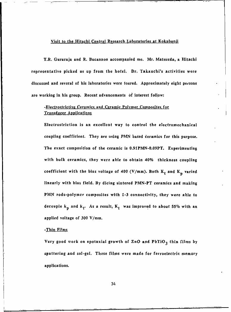
Visit to the Hitachi Central Research Laboratories at Kokubunji
T.R. Gururaja and R. Bucannon accompanied me. Mr. Matsuzda, a Hitachi
representative picked us up from the hotel. Dr. Takauchi's activities were
discussed and several of his laboratories were toured. Approximately eight persons
are working in his group. Recent advancements of interest follow:
-Electrostrictive Ceramics and-Ceramic Polymer Composites for
Transducer Applications
Electrostriction is an excellent way to control the electromechanical
coupling coefficient. They are using PMN based ceramics for this purpose.
The exact composition of the ceramic is 0.91PMN-0.09PT. Experimenting
with bulk ceramics, they were able to obtain 40% thickness coupling
coefficient with the bias voltage of 400 (V/mm). Both Kt and K variedt p
linearly with bias field. By dicing sintered PMN-PT ceramics and making
PMN rods-polymer composites with 1-3 connectivity, they were able to
decouple k and kt. As a result, K was improved to about 55% with an
applied voltage of 300 V/mm.
-Thin Films
Very good work on epotaxial growth of ZnO and PbTiO 3 thin films by
sputtering and sol-gel. These films were made for ferroelectric memory
applications.
34

Visit to-Nippon Soda at Odawara
Mr. Kato, manager of the ceramic group, picked me up from the hotel.
After about two hours of traveling by train, we arrived at Odawar City. He
gave me a brief tour of the city prior to arriving at the Research Center.
This is a chemical company which is in very strong collaboration with NEC.
In fact, NEC obtains most of the powders from -Nippon Soda.
Ma ior Activities
Processing -of Relaxor Ferroelectric -Materials
- Namely PMN-PNN composition prepared by alkoxide methcd and also by
high energy attrition milling. Three engineers are working full time-on this
project. The powder prepasred by this company meets the requirements high
reliability MLC's.
Tape Castin!
- Two enginieers working full time on the effects preparation and property
evaluation of thin layers of tape relaxor of the materials.
Superplasticity of Transformation Tpughened Ceramics
- The goal is to enhance the creep rate at Which large superplastic
deformations take place. They are studying the effect of the additives such
as Fe, Mn, (Fe+b), V2 05, Bi 2 0 3 to 3Y-TZP which may yield a liquid grain
35

boundary phase at low temperature. In the evening, Dr. Isehi, the executive
vice-president of the company plus three other top people in manageriail
positions members of the company spent the whole evening with me.
Visit to Mitsubishi Materials Inc. at Kanagawa
- In the morning of December 19. I visited Dr. Sato's group briefly.
- Mainly interested in ferroelectric and superconducting thin films. Very
good work on superconducting thin films by MOCVD and laser deposition
but in ferroelectric thin films they are far behind.
SUMMARY
The 5th US - Japan Seminar was organized extremely well. There werevery
good interactions and productive discussions between the US and Japanese
participants. Visiting the Japanese industries was very useful and a good
experience for me. I think the new "Pb free" piezoelectric ceramics,
piezoelectric fiber and electrostrictive ceramics and composites for
controlled Kt were the highlight of the meeting. I believe that this seminar
series should continue and participation from US industry should be
expanded. I would like to take this opportunity to thank the Office of
Naval Research for sponsoring my trip.
36
DISCUSSIONOF THE
5TH UNITED STATES-JAPAN SEMINARON
DIELECTRIC AND PIEZOELECTRIC CERAMICS
December 11-14, 1990Kyoto, Japan
Prepared by
Walter A. Schulzeof
New York State College of Ceramicsat
Alfred University
37

1.0 Introduction
This report will be divided into three sections. The first is generalobservations from the meeting and discussions with participants that donot fit with the evaluation of specific posters in the second section. Thethird portion is a brief review of a visit to the Shanghai Institute ofCeramics that occurred directly after the meeting.
2.0 General Observations
My general observation from the meeting four years ago still seemsvalid; that is, the Japanese companies, in general, still seem to becommitting a considerably larger fraction of their gross revenues intoresearch and development, especially development, than their UnitedStates counterparts. The emphasis is still on products and the Japanesecompanies are not unwilling to consider very new and advanced processingtechniques to gain the ability to produce advanced devices before a markethas assured a sales advantage. Part of the perceived Japanese dominancein the research and development area may also come from the willingnessof Japanese companies to present what appears to be relatively currentdevelopment work. It was very interesting to hear that only about twothirds of the Japanese companies that wanted to attend were allowed toparticipate in the meeting. It was stated that about one half as many aswe met were turned away. At this point, it is interesting to observe thatDr. Kenji Uchino was conspicuously absent with rumors ranging from a fallout with the organizers because of his strong industrial connections toexhaustion. I am not strong in my information, but I believe the facts lietoward the latter complicated by a possible career change. Also, it isinteresting that the proximity of the meeting still did not warrant ashowing from Kyocera. This may be because of Murata's traditionallystrong support of the seminar series. Even the AVX (Kyocera)representative from the United States failed to show.
One of the highlights of the meeting was to see 15 United Statesindustrial participants in the book. This is a major increase from fouryears ago and especially so in the light of our "recession". Figurespresented by Joe Dougherty indicated United States-Japanese attendancefigures as 18:26 for universities, 15:56 for industry, and 6:2 forgovernment representatives. This good United States turnout is the result
38

of efforts by Joe and others to involve industry (lacking four years ago)
and the Navy funding that aids university personnel like myself.
3.0 Comments on Selected Papers
P-1 Excellent presentation and shows the very good film workprogressing in the United States. This demonstrates how military fundingcan boost a very marketable technology, if only United States industrywill take the advantage.
P-2 The selection of Dr. Hirano by the Japanese for their leadposition just adds more emphasis to my feeling that he is a researcher towatch for innovations in processing.
1-3 As usual, Dr. Cross is getting to the heart of understandingrelaxor materials as many of us only wish we could.
1-4 Dr. Nishigaki again uses a complex chemical approach, even forJapanese, and makes it work. This demonstrates the willingness tocommit a large effort to develop a product even for a saturated market.
1-6 I do not remember Taiyo Yuden having previous Ni electrodetechnology. It appears they are stabilizing resistivity with Mg on a B siteas is done with Ca.
I-8 Looks like excellent hydrothermal preparation of bariumtitanate.
1-9 I believe using the Curie Weiss tail of a traditional relaxor isa new approach to developing a high-voltage dielectric.
1-13 It is interesting to see a worker of Dr. Igarashi's caliber pushmulticompositional multilayers. The idea is sound; but until now, industryhas been skeptical of processing problems.
1-23 Dr. Wakino continues to display a very sophisticated approachto the development of high-frequency dielectrics and theircharacterization.
11-2 and 3 The Prokopowicz formula continues to show
39

usefulness in life time projection.
11-5 IBM is becoming more secure in their low-fire coppersubstrate technology and seems to have overcome the removal of organicsat low temperature in a nonoxidizing system.
11-9 and 10 These show the recognition of the need for morebasic studies to develop better adhesion in thick-film materials.
11-13 The connection between Yamamoto and Igarashi is clear herewith both working on multicompositional multilayers to average or sumproperties.
11-14 Dr. Hirano is another to watch for excellent organicpreparation techniques.
11-15 Tom Shrout's smart calcining is an inexpensive alternativeto organically-prepared powder.
11-18 DuPont's coating process gives a view of next-generation-powder preparation for rheology control.
11-19 Fibrous single crystals are impressive from theoretical anddevice perspectives.
111-3 Interesting work. Apparently the field resulting from ashort circuit boundary condition can actually increase cycle lifetime.
111-4 Always good to see Bert Auld working in piezoelectriccomposites.
111-9 Does this mean ceramic-containing composites are winningagainst PVDF in the hydrophone race?
111-10 i sometimes wonder about so many players in the PMNgame. I also wish I had asked more about lead safety and lead scrapdisposal in Japan.
I1-11 and 12 Good to sec a serious player like Takeuchi in thebiased-electrostrictor development. This is a transducer area that should
40

have taken off years ago.
111-14 Very interesting low-lead-piezoelectric system thatshould be explored. How is the patent coverage of this one?
111-17 I do not remember previously seeing this type of rotationaldisplacer.
111-18 and 19 More interesting motion devices from Japan.
111-22 As a result of this meeting I finally understand, from aferroelastic-domain-reorientation concept, why the indent cracks aredifferent lengths; but it came from discussions, not from the poster.
IV-2 Thin film work is obviously being explored in Japan for allmarket areas.
IV-6 and 8 Many normal and less obvious film-forming techniquesare being explored.
IV-9 This is a most impressive film-forming iechnique. Theability to follow substrate contours is excellent.
IV-20 The PLZT samples by Nagata were physically veryimpressive and may represent an increase in possible device size if theyare spatially consistent.
4.0 Shanghai Institute of Ceramics
My visit to Shanghai Institute of Ceramics was hosted by Dr. ChudeFeng, who spent a year as a visiting scholar at the Now York State Collegeof Ceramics. The rational for using the short period of time available forvisitation after the United States-Japan Seminar was that I knowessentially nothing about the conditions for ceramic research anddevelopment in China. Also, this is the only time I could afford to makethe visit. I found it most educational!
Probably the most important realization was the level of living andworking conditions. I knew China was not a rich country, but I also was
41

aware of the expensive equipment in operation in Shanghai. The workersthere are to commended for the very good research conducted in an old,unheated, concrete facility, which was not really constructed for researchwith poor maintenance and janitorial services. The difficulties seem tobe overcome by skilled, patient individuals and careful work.
As would be expected, much of the equipment is imported with thedominate share from Japan and the United States. The choice seems toshow careful and cost-conscious selection. The choice of projects seemsto be driven by careful analysis of external literature and internal need.The Institute is very conscientious about developing profitable productsand eliminating the need for foreign purchase of ceramic materials. As aproject reaches the prototype level, it is transferred to the Research andDevelopment facility about 30 miles away. This group of two-storybuildings has a much more campus feeling, and the buildings seem to beconstructed for the purposes.
At the Institute I was greeted by Drs: Yin and Guo. This wasfollowed by visits to a host of departments. The visit to the structuralmaterials area was conducted by the section leader, Dr. Jiang Dong Liang.Material projects ranged from hydrothermally-prepared, nano-size powderof stabilized zirconia to a pressurized furnace for preparing siliconnitride.
The mechanical properties testing facilities were supervised byTing Rong Lai and included high-temperature three-point bend,indentation, and a computer-monitored group of high-temperature creepfurnaces.
The single crystal area was described by Deputy Director, Fan Shiji.This area was impressive from the old crystal pulling equipment use fordevelopment to the incredibly sophisticated BGO crystals produced forCERN. Development has now turned to fluoride systems. Diamondproduction still seems to be a strong cash product. The work ranges fromseeded large crystal production to sintered diamond coating for cuttingtools.
In the electronic ceramics area, I was told that lead-based capacitorformulations had been successfully transferred to a production facility.The current thrust was demonstrated by a new, very clean area dedicated
42

to the production of PTCR barium titanate heater material. The bariumtitanate is produced from barium carbonate and titania very similar toolder United States commercial systems.
I was honored by an evening banquet which was attended byProfessors Guo, Yin and Feng. I was very happy to meet Chen Zhili againafter a number of years. The professors were not sure ,;he would make thedinner since she is ranked either third or fourth in Shanghai as Head of theMinistry of Propaganda. It is a good feeling to realize that a competentscientist and good person can rise to such a position.
43

Trip Report-Fifth U.S.-Japan Seminar
on Dielectric and Piezoelectric Ceramics
B. A. AuldEdward L. Ginzton Laboratory
Stanford University
Stanford, CA 94305
Structure of the Meeting
The meeting was exceptionally well organized and the hospitality of our Japanesehosts was extraordinary. Indeed, such hospitality presents a challenge to the organizers of
the next meeting in the United States.
This is my second attendance at this series of meetings and my clear impression isthat progress has been made since the Toyama meeting. This type of meeting (a small
group, intensive meetings, and social gatherings in the evenings) is very effective inpromoting information exchange. In this particular meeting the facilities for the technicalsessions at the university and the social events at the hotel greatly enhanced the interactionsand discussions, both international and intranational. For me, a very pleasant surprise was
the degree to which I had extremely fruitful conversations with American colleagues andnew acquaintances. I made several valuable contacts, to be followed up in the future.
Also, the Japanese talked much more freely than ever-before in my experience.
The use of three minute introductions by the principal poster authors is an excellent
idea. This approach provided an information focus and a first contact with the authors thatsimplified the later viewing of the posters, and made the whole procedure more dynamic.
The Japanese presentations were much irnproved-over the rapporteur style of presentation
at Toyama. Someone has clearly spent time coaching their younger scientists on how to
summarize concisely and how to highlight their viewgraphs with colored cues-under-lining, arrows, etc. Some of the Americans could well have taken a few lessons from
some of the Japanese visual aids. The two plenary lectures were excellent although,perhaps, a little long. They were so effective that the next meeting could well include a
greater number of review lectures. I realize that time is limited and that the essence of this
44

meeting lies in the poster sessions. But it would be useful to consider having four thirty
minute lectures at the next meeting.
Technical Content
The plenary lectures on "Physics and Engineering of Ferroelectric Memories" and
"Chemical Processing of Electronics Ceramics" properly placed emphasis on the
technology of ferroelectric thin films. It is impressive to see the advances made in this area
since the Toyama meeting. In the Friday session on thin films and electrooptics the U.S.
and Japanese effort was quite well balanced (9 versus 11 posters, plus one joint effort).
Not unexpectedly there was a significantly greater contribution from industry among the
Japanese and from universities among the Americans. This partly reflects the research-
industrial structure in the two countries. But there remains also a problem in attracting
American industrial scientists to these meetings. Efforts to correct this situation shouldcontinue. It was surprising to find so few Japanese ultrasonic and acoustic device
engineers at this meeting. Less surprising because of the travel distance involved, was the
small representation of Americans working in both ultrasonics and actuators. An effort
should be made next time to invite selected attendance from the medical ultrasound and
general sensors industries.
In my particular speciality, piezoelectric composites, the high points of the meeting
were the poster presented by M. P. Harmer and J. Chen from Lehigh University on
modeling the dielectric properties of diphasic mixtures, and the poster presented by H.
Banno and K. Ogura of NTK on four-phase 0-3 composites. The first of these provides an
excellent formal base for our work on modeling 0-3 composites, and the second led to
stimulating conversations with H. Banno about the present status and future trends of the
Japanese effort. Lively discussions were also held with M. Kahn of the Naval Research
Laboratory on the subject of 3-0 composites. These highlights emphasize the intensive
intranational and international contacts that constitute for me the strength of these meetings.
45

Fifth US-Japan Seminar on Dielectrics and Piezoelectrics
Trip Report Gene Haertling
Monday, December 10, 1990
A visit was made to Nippon Mining Company, Ltd. Nippon Miningis a $5.1B company located about 1 hour from downtown Tokyo. Ithas assembled the largest concentrated effort in Japan on PLZT.Although they have focused on bulk materials for most of theirwork, they have also now initiated a program in thin film ferro-electrics utilizing a MOCVD technique. The abstracts of two papers(one not yet published) are attached to this report.
Accompanied by Dr. K. Nagata of the National Defense Academy(who claims to be the Japanese coordinator for PLZT in Japan), wespent the first part of the visit in presentations and discussionsof the research work on PLZT at Nippon Mining. Dr. Hideo Sagawa,the general manager and host, presented an overview of NipponMining and then left the technical presentations to the scientists,most of which were very young. Five individuals gave talks ontheir areas of expertise - these included (1) T. Tsukada on powderpreparation by chemical coprecipitation, (2) A. Nakajima ontapecasting, (3) R. Suzuki on sintering and hot pressing, (4) S.Okubo on evaluation and (5) A. Katoh on devices. The last part ofthe visit included a plant tour of the facilities dedicated to thePLZT work.
Points of interest:
1. The PLZT development work was started three years ago.
2. It was funded with government seed money and a 3-year effort toestablish a PLZT capability. Very good equipment was evidenteverywhere on the plant tour. This equipment is on loan from thegovernment to establish this capability and will need to bereturned within the next year. Examples of special equipmentinclude large batch chemical coprecipitation processing equipment,a vacuum/oxygen uniaxial hot press, a hot isostatic press (HIP), adiamond surfacing grinder, lapping and polishing equipment, acomputer-controlled slotting saw for electrodes, optical and IRspectrometers and E/O measuring apparatus.
3. The central research lab at Nippon Mining involves five separatelabs and 900 people. Subdivisions include: (1) inorganicmaterials, (2) organic materials, (3) ceramic materials, (4)petroleum products and (5) resins. Their research and developmentof the PLZT materials is part of (3).
4. The PLZT effort involves a group of 10 researchers working inthe specialty areas mentioned above.
46

5. They employ a different chemical preparation process for theirPLZT powder, using PbO, La203, ZrO(N03)2 and TiCl4.
6. The atmosphere sintering process for PLZT was pretty standardbut good, and the PLZT polished ribbon (1" x 12" x 0.1") producedfrom it is of excellent quality. It was prepared from tapecast/laminated material and was obviously fabricated for printer heads.
7. There was nothing new on devices - mostly shutters. I saw bothshadow evaporated electrodes and plated/slotted electrodes fortheir devices. The shutters I observed were of marginal qualitybecause they exhibited a residual space charge problem which wasobviously not addressed.
Overall Assessment
Nippon Mining now has the capability of producing good, opticalquality PLZT ceramics in quantity by either hot pressing orsintering and intends to supply the markets in Japan and elsewhere.Their progress in the last three years, from start-up to productdevelopment, has been very impressive. The issue of whether theyhave a cost effective product remains to be seen. This will beevident after the government funding goes away.
Tuesday, December 11, 1990
Tuesday was spent visiting NGK/NTK in Nagoya. Our host, Dr.H. Banno, introduced our group of US visitors to NGK and then tookus on a tour of the manufacturing facilities for piezoelectricfilters. The tour only included the last part of the productionprocess; i.e., (1) slicing/dicing of the filter blanks from thefired plates, (2) fired-on Ag electroding, (3) auto-poling, (4)auto-tuning and (5) final testing. Although we were not shown thematerials batching and processing areas, it was surmized that theywere using a PZT formulation (probably 52/48) with both Cr and Mnadditives.
In the manufacturing process shown to us, there was a largeamount of automation in place. Extensive use of computer-interactive data collection and quality control were evident.According to Banno, their yields were very high because computer-interacti e tuning of each individual filter assured them of theseresults.
In general, the line they showed us appeared to be veryefficient and well run. It was more automated than other linesthat I have seen at other companies in the US which deal withsimilar products. Much of their automation was their own; i.e., itwas designed in-house and made in-house for their own use,exclusively.
Late afternoon was spent traveling to Kyoto.
47
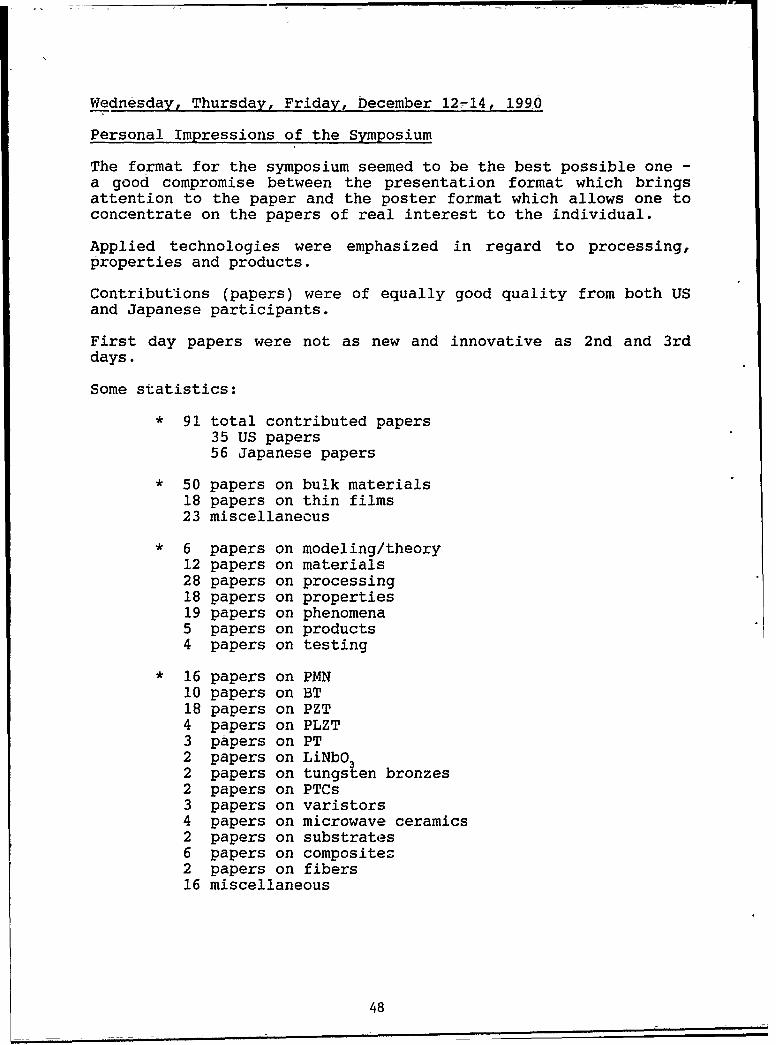
Wednesday, Thursday, Friday, December 12-14, 1990
Personal Impressions of the Symposium
The format for the symposium seemed to be the best possible one -
a good compromise between the presentation format which bringsattention to the paper and the poster format which allows one toconcentrate on the papers of real interest to the individual.
Applied technologies were emphasized in regard to processing,properties and products.
Contributions (papers) were of equally good quality from both USand Japanese participants.
First day papers were not as new and innovative as 2nd and 3rddays.
Some statistics:
91 total contributed papers35 US papers56 Japanese papers
* 50 papers on bulk materials18 papers on thin films23 miscellaneous
6 papers on modeling/theory12 papers on materials28 papers on processing18 papers on properties19 papers on phenomena5 papers on products4 papers on testing
16 papers on PMN10 papers on BT18 papers on PZT4 papers on PLZT3 papers on PT2 papers on LiNbO32 papers on tungsten bronzes2 papers on PTCs3 papers on varistors4 papers on microwave ceramics2 papers on substrates6 papers on compositez2 papers on fibers16 miscellaneous
48

Most popular materials at this symposium were PZT and PMN, and themost popular devices were actuators. Microwave ceramics and BTcapacitors were also prominent along with thin films.
Most innovative modeling concept was the tesselation-derivedmicrostructures of Penn State (S. Kurtz, et.al.)
Product papers were exclusively Japanese.
Summary
Making new contacts and renewing old ones was a pleasantexperience and of value, however, they were not critical to any newwork that I plan in the near future. Although I did not feel thatthere were any breakthroughs reported at this symposium, there weresome papers which in my mind stood out. These included:
1. Paper No. 111-14 dealing with the compositionBi Na TiO -PbTiO . This system contains lessless PF and could be a substitute for PZT whenlead compounds are restricted in the US in thefuture. In addition, it can be fired in an openfurnace which would be a distinct advantage.
2. Paper No. 11-18 involving chemical precipitationand coating processes for dielectric powders.This coating process can be important for possiblelower temperature sintering and new boundary-layercapacitors.
3. Papers 111-17, 111-18 and 111-19 utilizing PZT andPMN materials in actuator devices as torsionalvibrators, auto-focusing systems and linear motors.
In general, I observed a high level of interest in thesymposium and felt that it was worthwhile, albeit, more from theJapanese side than the US side. It appears that Okazaki's state-ment at the 1st Symposium in 1982; i.e., "Japan is too much inpractical improvement and not enough in scientific work" is stilltrue but it noticeably changing. On the other hand, it can also besaid that the US is still heavy on scientific research and notenough in technology and product applications. This may bechanging, but if it is, it is do so very slowly. As has beenobserved before and is still true, "in the long run, we (the US)will be the losers." Thin film ferroelectrics is now the newfrontier which has opened up a myriad of possibilities for newscience, technology and applications, especially integratedapplications. Let's hope that the US maintains a balanced approachto this new initiative.
49
DEPENDENCE OF ELECTRO-OPTICAL AND DIELECTRIC PROPERTIESOF PLZT CERAMICS IN PHASE BOUNDARY COMPOSITION
Shuuichi OHKUBO, Ryou SUZUKI, Hideo SEGAWA, Tsuneo SUZUKI
New Material Laboratory, Nippon Mining Co., Ltd., 3-17-35, Niizo-minami,Toda-shi, Saitama-ken, 335 Japan
For determining the composition region suitable for PLZT optical shutter utilizing
second-order electro-optical effect, various PLZT compositions of phase boundary
region compositions were prepared, and dielectric, electro-optical characteristics
were examined. As the result, it has been found that the value of ratio of remanent
polarization to spontaneous polarization is suitable as the factor for determining
whether the electro-optical effect is good or not, and the composition of 8/70/30 is
suitable when applied to optical shutter.
PREPARATION AND ELECTRICAL PROPERTIES OF PZT THIN FILMS BY MOCVD
Yukio Sakashita, ToshlyukI Ono, Hideo Segawa
Materials Development Research Laboratories, Nippon Mining Co., Ltd.
Toda, Saltama 335, Japan
Kouji Tominaga, Masaru Okada
Faculty of Engineering, Chubu University
Kasugal, Aichl 487, Japan
Strongly [O1 oriented lead zirconate-titanate (Pb(ZrxTi,-.)O3) thin
films with te(ragonal structure (0<x<0.52) have been successfully grown
on (I00)Pt/(OO)MgO substrates by using metal-organic chemical vapor
deposition (:XOCVD). The metal-organic precursors were Pb(C2H6)4, Zr(DPM)4
and TI(I-OC3ii7)4. Scanning electron mlcrographs showed dense and
noncolumnar growth with good surface morphology. The relative dielectric
constants at room temperature were 200-350, and appeared to have less
dependence on composition x than PZT bullk ceramics. Typical D-E hysteresis
loops which occur with PZT bulk ceramics were observed. Remanent
polarizations were 30-40/AgcO2 .The coercive field decreased from 65kY/cm
to 40kV/cm with Increases In Zr content. The pyroelectrlc coefficients
without poling treatment were about 3xlO-'C/cm2K, showing almost the same
value as that of poled PZT bulk ceramics.
50
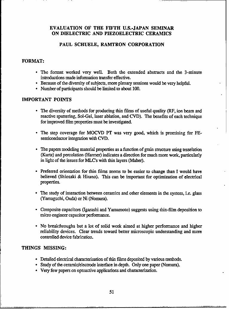
EVALUATION OF THE FIFTH U.S.-JAPAN SEMINARON DIELECTRIC AND PIEZOELECTRIC CERAMICS
PAUL SCHUELE, RAMTRON CORPORATION
FORMAT:
• The format worked very well. Both the extended abstracts and the 3-minuteintroductions made information transfer effective.
• Because of the diversity of subjects, more plenary sessions would be very helpful.- Number of participants should be limited to about 100.
IMPORTANT POINTS
" The diversity of methods for producing thin films of useful quality (RF, ion beam andreactive sputtering, Sol-Gel, laser ablation, and CVD). The benefits of each techniquefor improved film properties must be investigated.
" The step coverage for MOCVD PT was very good, which is promising for FE-semiconductor integration with CVD.
* The papers modeling material properties as a function of grain structure using tesselation(Kurtz) and percolation (Harmer) indicates a direction for much more work, particularlyin light of the issues for MLC's with thin layers (Maher).
* Preferred orientation for thin films seems to be easier to change than I would havebelieved (Shiosaki & Hirano). This can be important for optimization of electricalproperties.
* The study of interaction between ceramics and other elements in the system, i.e. glass(Yamaguchi, Onda) or Ni (Nomura).
" Composite capacitors (Igarashi and Yamamoto) suggests using thin-film deposition tomicro engineer capacitor performance.
* No breakthroughs but a lot of solid work aimed at higher performance and higherreliability devices. Clear trends toward better microscopic understanding and morecontrolled device fabrication.
THINGS MISSING:
• Detailed electrical characterization of thin films deposited by various methods.
• Very few papers on optoactive applications and characterization.
51

1 University of Colorado at Boulder
Department of Physics
Condensed Matter LaboratoryCampus Box 390Boulder. Colorado 80309-0390(303) 492-1515FAX: (303) 492-2998
27 Dec 1990
REPORT ON THE 5th US-JAPAN SEMINAR ON DIELECTRIC AND
PIEZOELECTRIC CERAMICS
As a researcher whose work is almost equally divided between
academic university programs and industrial R&D, I found the
mix of people and papers at this conference particularly
pleasant. My own special area of interest is in ferroelectric
thin film memories. Most of the papers in this area were
presented on the third day, and some were quite innovative:
I particularly liked the excimer-laser ablation-deposition of PZT
reported by Krupanidhi; his dep rate of 1 micron in 20 minutes
was quite impressive. The result of Dey on high-voltage switching
of sol-gel PZT films was also quite noteworthy; by constructing
a high-voltage, ns risetime driving circuit for his PZT RAMs,
he was able to show two distinct characteristic activation
fields for switching, one of which "turns on" at 300-350 kV/cm.
(I suspect that this is the threshold between inhomogeneous
nucleation at the electrode interfaces and homogeneous nucleation
throughout the film.) On the more basic side, Prof. Cross'
study showing the analogous relationship between magnetic spin
glasses and relaxor ferroelectrics appears quite profound and is
likely to be the seed for a very large number of studies in the
immediate future.
On the Japanese side the paper by Prof. Shiosaki showing
virtually perfect submicron step coverage of PZT on Si via
CVD deposition was startling in the quality of coverage
produced. It was without question the Japanese paper of greatest
interest to me. Second would rank the plenary review by Hirano,
which was delivered in excellent English and full of good new
information.
52

As in any good conference, the really important imformation is
transmitted in the hallways or after dinner. Such was the case
in Kyoto. I was particularly interested in understanding the
level of interest and activity within Japanese industrial
iaboratories for the application of ferroelectric thin films in
both DRAMs (for higher capacitance to minimize trenching problems
64Mb DRAMs) and for ferroelectric RAMs. Surprisingly, this
activity is not limited to companies like NEC and Matsushita,
where it might be expected, but also spills over into
corporations that are not into high-density memories, such as
the capacitor manufacturers (Murata and Kyocera). There is not
such interest in vertical integration among US corporations of
the same size and technical orientation.
After the conference I was fortunate to be invited to give a
plenary lecture at a meeting of JEIDA, the Japanese Electronics
Industry Association, in Tokyo. At this talk there were
technical representatives from the following Japanese
corporations: Oki Electric Co., Canon, Sharp, Seiko, Sony, TDK,
Toshiba, Nishin Denki, Japan Signal Co., NEC, JVC, Hitachi,
Fuji-Xerox, Fujitsu, Matsushita, Mitsubishi, Murata, Yokagawa,
Ricoh, Sumitomo Chemical, and Fuji Electric Co., among others.
For me this was a unique opportunity to present the results of
my efforts over the past five years to develop f-irroelectric
memories in Colorado, and to exchange technical ipformation with
leaders of Japanese microelectronics industries. There is,
however, a sad comparison to be made with the level of interest
in this technology found in US industries, where only a handfull
are doing work (Westinghouse, TRW, McDonnell-Douglas, Raytheon)
and almost entirely with DOD funds rather than in-house IR&D.
As it stands, these US-Japan symposia are excellent, but unless
more US industries can be coerced into participation, they risk
being technology-transfer avenues between US universities and
Japanese industries, which is not altogether healthy.
of. J. F. Scott
University of Colorado53

FIFTH U.S. - JAPAN WORKSHOP ON DIELECTRIC
AND PIEZOELECTRIC CERAMICS
Report by
Professor Martin P. HarmerMaterials Research CenterLehigh UniversityBethlehem PA 18015 USA
On 11-14 December 1990 I attended the Fifth U.S.- Japan Seminar onDielectric and Piezoelectric Ceramics in Kyoto, Japan. Prior tothe meeting I visited Professor Niihara at Osaka University tolearn about their work on "nanocomposites". They reported thatthe incorporation of small amounts (5-10 vol%) of "nano" - sized(0.3 micron diameter) SiC particles into various ceramics couldsignificantly enhance the strength. Obtaining a-uniformdispersion of the SiC particles is crucial to the attainment ofhigh strength. In confirmation of their result3, we have sinceobtained strengths in our laboratory of over 1000 MPa on hotpressed alumina containing 5 vol % SiC particles. For comparison,the undoped alumina had an average strength of 560 MPa. I am notaware of other groups in the U.S. pursuing this approach. Theseminar itself covered a wide exchange of information on severaltopics and I will just make some general. observations here.Firstly, it was clear that there has been significant growth inthe area of ferroelectric thin films for use in non volatilecomputer memory and DRAM applications. Researchers from Muratadescribed a novel hydrothermal electochemical technique forproducing high quality thin films at very low temperatures (100 -200 degrees C). Overall, the U.S. and Japan seemed to be makingcomparable progress in this field. Piezoelectric compositesappear to have reached a mature stage of development.Piezoelectric motors and high strain actuators are being developedextensively in Japan for a variety of applications, whereas theU.S. activity in this area is very small. U.S. capacitorcompanies have been reluctant to develop lead based relaxorferroelectrics for capacitor applications, whereas Japanesecompanies have steadily been introducing relaxors into thecapacitor business. Both in Japan and the U.S. the technology forreducing the thickness of the dielectric layers in multilayercapacitors has been improved. Minimum thicknesses in the range of5 - 10 microns are now routinely achievable.
54

LIST OF U.S. PARTICIPANTS
James H. Adair Nicholas G. Eror121 Rhines Hall University of PittsburghDept. of Materials Science Department of Materials Scienceand Engineering and EngineeringUniversity of Florida 848 Benedum HallGainesville, FL 32611-2066 Pittsburgh, PA 15261
Bert Auld Steve Freiman
Stanford University NIST
Edward L. Ginzton Lab Building 223
Stanford, CA 94305 Room A329Gainthersburg, Md 20899
Amar S. Bhalla T. R. GururajaPenn State University Hewlett-Packard Company253 Materials Research Laboratory 3000 Minuteman RoadUniversity Park, PA 16802 Andover, MA 01810-1099
Relva Buchanan Gene H. HaertlingUniversity of Illinois Clemson UniversityMaterials Science and Engineering 206 Olin Hall105 S. Goodwin Ave. Clemson, SC 29634Urbana, IL 61801
Ian Bum Martin HarmerE. I. DuPont de Nemours, Inc. Lehigh UniversityE334 Materials Science and Engineering
Experimental Station Whitaker Lab, No. 5Wilmington, DE 19880-0334 Bethlehem, PA 18015
James Canner Peter JessonMurata Erie N. A., Inc. DoPont Chambers Works
1990 West College Ave. Jackson Lab 211
State College, PA 16801 Deepwater, NJ 08023
M. S. Chu Manfred KahnTAM Ceramics Inc. Naval Research Laboratory4511 Hyde Park Bivd. Code 6360Niagara Falls, NY 14305 Washington, DE 20375
L. Eric Cross Angus Kingon
Penn State University North Carolina State University
167 Materials Research Laboratory Materials Science Dept.University Park, PA 16802 Box 7907
Raleigh, NC 27695
Standwip K. Dey Barry G. KoepkeAlizona State University Honeywell, Inc.CBME Dept. Underseas Systems Division177 Engineering Research Center 5121 Wmnnetka Avenue N.Tempe, AZ 85287 New Hope, MN 55428
Joseph P. DoughertyPenn State University S. B. Krupanidhi144 Materials Research Laboratory Penn State UniversityUniversity Park, PA 16802 150 Materials Research Laboratory
University Park, PA 16802L. N. DurvasulaDARPA DSO Office S tewart K. Kurtz1400 Wilson Blvd. Penn State UniversityArlington, VA 22209 202 Materials Research Laboratory
University Park, PA 16802
55

LIST OF U.S. PARTICIPANTS
Hung C. Ling James F. Scott
AT&T Bell Labs University of Colorado, Boulder
Box 900 Department of Physics
Princeton, NJ 08540 Campus Box 390Boulder, CO 80309-0390
Gordon LoveALCOA Thomas R. ShroutALCOA Technical Center Penn State UniversityAlcoa Center, PA 15069 150 Materials Research Laboratory
University Park, PA 16802Galeb H. Maher
MRA Laboratories Wallace A. SmithAdvanced Ceramics Group Office of Naval Reseach96 Marshall Street 619 Ballston TowerNorth Adams, MA 01247-2411 800 N. Quincy Street
Arlington, VA22217R. R. NeurgaonkarRockwell International Donald M. SmythScience Center . Lehigh university1049 Camino Dos Rios Materials Research CenterBox 1085 Coxe Lab, Building 32Thousand Oaks, CA 91360 Bethlehem, PA 18015
Alan Rae Donald K. SwansonTAM Ceramics Inc. DuPont Chambers Works4511 Hyde Park Blvd. Jackson Lab 211Niagara Falls, NY 14305 Deepwater, NJ 08023
Kim Richie Bob TingAVX Corp. NRLBox 867 Underwater Sound Ref. DivisionMyrtle Beach, SC 29577 Box 8337
Orlando, FL 32856Ahmad Safari
Rutgers University Rao R. TummalaBox 909 IBM CorporationPiscataway, NJ 08854 East Fishkill Facility
Dept. 25Y, Bldg. 330Paul Schuele Zip 81A, Route 52Ramtron Corp. Hopeweel Junction, NY 125331873 Austin Bluffs ParkwayColorado Springs, CO 80918 S. Vankataramani
General Electric Central ResearchWalter A. Schulze Building KIAlfred University Room MB-149McMahon Building Box 8Alfred, NY 14802 Schenectady, NJ 12301
56
LIST OF-JAPANESE PARTICIPANTS
K.Abe Koya HayashiResearch and Development Division Research and DevelopmentSakai Chemical Industry Co., Ltd. Shoei Chemical Inc.5-1 Ebisujima, Sakai Shinjuku Mitsui BuildingOsaka 590, Japan 1-1, Nishishinjuku 2-Chome
Tokyo 163, JapanToshinori AndoR&D Laboratories-I K.HidakaNippon Steel Corporation Research and Development Division1618 Ida,'Nakahara-ku Sakai Chemical Industry Co., Ltd.Kawasaki 211,-Japan 5-1 Ebisujima, Sakai
Osaka 590, JapanM.AokiResearch and-Development Division Shin-ichi HiranoSakai Chemical Industry Co., Ltd. Department of Applied Chemistry5-1 Ebisujima, Sakai Fuculty of EngineeringOsaka 590, Japan Nagoya University
Furo-cho 66, Chikusa-kuAkira Baba Nagoya 464-01, JapanHachindhe Institute of Technology-88-1 myo, Oobiraki, Hachinohe Toshihisa HondaAomori 031, JApan Materials & Electronic
Devices LaboratoryHisao Banno Mitsubishi Electric Corp.NTK Technical Ceranics Diyision 1-1-57 Miyashimo, Sagamihara-shiNGK Spark Plug Co., Ltd. Kanagawa 229, Japan14-18 Takatsuji-cho, Mizuho-kuNagoya 467-91, Japan N.Ichinose
Department of Materials ScienceHirokazu'Chazono. and EngineeringTaiyo Ytden Co. Ltd. School of Science and Engineering1660 Kamisatomi Harina-rmachi Waseda UniversityGunnia-gun, Gunma 370-33, Japan 3-4-1 Ohkubo, Shinjuku-ku
Tokyo 169, JapanS.C.ChoiPCAST, H.IgarashiThe University of Tokyo Dept. of Electrical Engineering4-6-1 Komaba, Meguro-ku The National Defence AcademyTokyo 153, Japan 1-10-20 Hashirimizu
Yokosuka 239, JapanKoichi FukudaElectronic Materials Research Group K.KobayashiUbe Laborafory- Research LaboratoryUBE Industries Ltd. OKI Electric Industry Co., Ltd.1978-5 Kogushi, Ube-shi 550-5 Higashiasakawa-choYamaguchi 755, Japan Hachioji-shi, Tokyo 193, Japan
Osamu Furukawa Kazuyuki KakegawaResearch and Development Center Faculty of EngineeringToshiba Corporation Chiba University70 Yanagi-cho, Saiwai-ku 1-33 Yayoi-cho, Chiba-shiKawasaki 210, Japan Chiba 260, Japan
Yukio Hamaji H.KatoMurata Manufacturing Co., Ltd. Narumi China Corporation2-26- 10 Tenjin, Nagaokakyo-shi 3 Denjiyama, Narumi-choKyoto 617, Japan Midori-ku, Nagoya 458, Japan
Fumio Hamano Junichi KatoCorporate Technology Materials and Devices Research Lab.and Planning Division Matsushita Electric Industrial Co., Ltd.Kyocera Corporation 1006 Kadoma Osaka 571, Japan5-22 Kitainoue-cho, HigashinoYamashina-ku, Kyot6 607; Japan

LIST OF JAPANESE PARTICIPANTS
K.Kikuta H.NagataDepartment of Applied Chemistry Tokyo Research CenterFuculty of Engineering Tosoh CorporationNagoya University 2743-1 Hayakawa, Ayase-shiFuro-cho 66, Chikusa-ku Kanagawa 252, JapanNagoya 464-01, Japan Kunihiro Nagata
Ryozo Kitoh Dept. of Electrical EngineeringElectronic Materials Research Group The National Defence AcademyUbe Laboratory 1-10-20 HashirimizuUBE Industries Ltd. Yokosuka 239, Japan1978-5 Kogushi, Ube-shiYamaguchi 755, Japan Hirohiko Nakahara
Department of Industrial ChemistryMitsue Koizumi Faculty of EngineeringJRCST The University of TokyoRyukoku University 7-3-1 Hongo, Bunkyo-kuYokotani 1-5, Oe-cho, seta Tokyo 113, JapanOtsu, Shiga 520-21, Japan
M.Nakanishi
Makoto Kuwabara Sumitomo Metal Industries, Ltd.Department of Applied Chemistry Research and Development DivisionKyushu Institute of Technology No.3 1-chome, Nishinagasuhondori1-1 Sensui-cho, Tobata Amagasaki, Hyogo 660, JapanKitakyushu 804, Japan Shoichi Nakano
Jingyu Lian Functional Materials Research CenterDepartment of Electronics SANYO Electric Co., Ltd.Faculty of Engineering 1-18-13 Hashiridani, HirakataKyoto University Osaka 573, JapanYoshida Honmachi, Sakyo-kuKyoto 606, Japan S.Nishigaki
Narumi China CorporationYoichiro Masuda 3 Denjiyama, Narumi-choHachinohe Institute of Technology Midori-ku, Nagoya 458, Japan88-1 myo, Oobiraki, HachinoheAomori 031, Japan M.Nishimura
Central Research LaboratoryHiroshi Masuzawa Kyocera CorporationCentral Research Laboratory 1-4 Yamashita-cho, KokubuHitachi Ltd. Kagoshima 899-43, JapanKokubunji, Tokyo 185, Japan
Takeshi NomuraToshiharu Minamikawa Materials Research CenterIndustrial Research Institute of TDK CorporationIshik'wa Prefecture 570-2 Mtsugashita, Minami-HatoriRo-1 Tomizu-machi Narita-shi, Chiba 286, JapanKanazawa-shi 920-02, Japan
Atsushi OchiT. Miyata Material Research LaboratoryResearch Laboratory Fundamental Research LaboratoriesOKI Electric Industry Co., Ltd. NEC Corp'ration550-5 Higashiasakawa-cho 4-1-1 Miyazaki, MiyamaeHachioji-shi, Tokyo 193, Japan Kawasaki 213, Japan
Kanji Murano Kohji OguraResearch Laboratories NTK Technical Ceramics DivisionSony Corporate NGK Spark Plug Co., Ltd.6-7-35 Kitashinagawa, Shinagawa 14-18 Takatsuji-cho, Mizuho-kuTokyo 141, Japan Nagoya 467-91, Japan
Akira Nagai Tomeji OhnoOdawara Research Center TOKIN CorporationNippon Soda Co., Ltd. 6-7-I Koriyama, Taihaku-ku345 Takada, Odawara Sendai, Miyagi 982, JapanKanagawa 250-02, Japan
58

LIST OF JAPANESE PARTICIPANTS
A.Okamoto Kenichi ShibataMaterials Research Center Functional Materials Research CenterTDK Corporation SANYO Electric Co., Ltd.570-2 Matsugashita, Minami-Hatori 1-18-13 Hashiridani, HirakataNarita-shi, Chiba 286, Japan Osaka 573, Japan
T.Okamura Hiroshi ShimizuTokyo Research Center Univ. of Electro-CommunicationsTosoh Corporation Chofugaoka 1-5-12743-1 Hayakawa, Ayase.shi Chofu, Tokyo 182, Japan.angawa 252, Japan
Masaru ShimizuHiroshi Okano Department of ElectronicsFunctional Materials Research Center Faculty of EngineeringSANYO Electric Co., Ltd. Kyoto University1-18-13 Hashiridani, Hirakata Yoshida Honmachi, Sakyo-kuOsaka 573, Japan Kyoto 606, Japan
Kiyoshi Okazaki Tadashi ShiosakiDepartment of Materials Science Department of Electronicsand Ceramic Technoltgy Faculty of EngineeringShonan Institute of Technology Kyoto University1-1-25, Tujido-Nishikaigan Yoshida Honmachi, Sakyo-kuFujisawa 25 1, Japan Kyoto 606, Japan
Hiromu Ohuchi Shin-ichi ShirasakiDepartment of Materials Science National Institute for Researchand Ceramic Technology in Inorganic MaterialsShonan Institute of Technology 1-1 Namiki, Tsukuba City1-1-25, Tujido-Nishikaigan Ibaraki 305, JapanFujisawa 251, Japan Sunao Sugihara
Kiyoshi Onda Department of Materials ScienceNarumi China Corporation and Ceramic Technology3 Denjiyama, Narumi-cho Shonan Institute of TechnologyMidori-ku, Nagoya 458, Japan 1-1-25, Tujido-Nishikaigan
Fujisawa 251, JapanHiroshi OnumaWilbur-Ellis Co., (Japan) Ltd. Ryuji SuyamaElectronic Materials and Devices R&D Laboratories-I308-314 Sanshin Building Nippon Steel Corporation1-4-1 Yurakucho, Chiyoda-ku 1618 Ida, Nakahara-kuTokyo 100, Japan Kawasaki 211, Japan
Kunio Saegusa Masasuke TakataTsukuba Research Laboratory Dept. of Electrical EngineeringSumitomo Chemical Co. Nagaoka University of Technology6 Kitahara, Tsukuba 1603-1 Kamitomioka, NagaokaIbaraki 330-32, Japan Niigata 940-21, Japan
Yukio Sakabe Tadashi TakenakaMurata Manufacturing Co., Ltd. Faculty of Science and Technology2-26-10 Tenjin, Nagaokakyo-shi Science University of TokyoKyoto 617, Japan Noda, Chiba 278, Japan
Koichiro Sakata Hiroshi TakeuchiFaculty of Science and Technology Central Research LaboratoryScience University of Tokyo Hitachi Ltd.Noda, Chiba 278, Japan Kokubunji, Tokyo 185, Japan
Housaku Sato Shigeru TanakaResearch Laboratory Hitachi Res. Lab. Hitachi Ltd.OKI Electric Industry Co., Ltd. 3-1-1 Saiwaicho, Hitachi-shi550-5 Higashiasakawa-cho Ibaraki 317, JapanHachioji-shi, Tokyo 193, Japan 59 -

LIST OP JAPANESE PARTICIPANTS
T6shio Tanimoto Nobutatsu YamaokaDepartment of Materials Sience Taiyo Yuden Co. Ltd.and Ceramic Technology 43-1 Yahatabara-cho, Takasaki-shiShonan Institte of Technology Gunma 370-11, Japan1-1-25., Tujido-NishikaiganFujisawa 25 lJapan Yohachi Yamashita
Research and Developement CenterK.Terao Toshiba CorporationSumitomo MetM Industries, Ltd. 70 Yanagi-cho, Sawai-ku16 Sunayama, Hasaki-machi Kawasaki 210, JapanKashima-gun, Ibaraki 314-02, Japan Takashi Yamaguchi
Junichi Toyoda Faculty of Science and TechnologyResearch Laboratories, Keio UniversitySony Corporate 3-14-1 Hiyoshi, Kohoku-ku6-7-35 KitashinagaWa Yokohama 223, JapanShinagawa-ku, Tokyo 141, Japan Takashi Yaaguchi
Ichiro Ueda Research and Deveropement CenterCentral Research Raboratory Mitsubishi Mining & Cement Co., Ltd.Matsushita Electric Industrial Co., Ltd. 2270 Yokoze, Chichibu-gun3-15 Yigumo-nakamachi Saitama 368, JapanMoriguchi, Osaka 570, Japah Taka-aki Yasumoto
Kikuo Wakino Research and Development CenterMurata Manufacturing Co., Ltd. TOSHIBA Corporation2-26-10 Tenjin, Nagaokakyo-ihi I Komuka Toshiba-choKyoto 617. Japan Saiwai-ku, Kawasaki 230, Japan
Akira Yamadar Tetsuo YoshidaMaterials.& Electronic TOKIN CorporationDevices.Laboratory. 6-7-1 Koriyama, Taihaku-kuMitsubishi Electric Corp. Senda, Miyagi 982, Japan1-1-57 Miyashimo. SagarniharaKanagawa 229, Japan Tetsuo Yoshimoto
Odawara Research CenterKoichi Yamada Nippon Soda Co., Ltd.Tsukuba Research Laboratory 345 Takada, OdawaraSumitomo Chemical Co. Kanagawa 250-02, Japan6 Kitahara, TsukubaIbaraki 330-32, Japan
Takashi Yam amotoDept.of Electrical Engineering Masatoshi AdachiThe National Defence Academy Toyama Prefectural University1-10-20 Hashirimizu 5180 Kurokawa,Kosugi-choYokosuka 239, Japan Imizu-gun, Toyama 939-03, Japan
Shosaku Yamanaka Hiroshi MaseItami Research Laboratories Mitsui Petrochemical Industries Ltd.Sumitomo Electric Industries, Ltd. 580-32 Nagaura, Sodegaura-machi1-1, Koya-kita 1-chome, Itami Kimitsu-gun, Chiba 299-02, JapanHyogo 664, Japan Hisakazu Takahashi
Hiroyasu Yamaoka Functional Materials Research CenterMitsui Petrochemical Industries Ltd. SANYO Electric Co., Ltd.580-32 Nagaura, Sodegaura-machi 1-18-13 Hashiridani, HirakataKimfiitsu-gun, Chiba 299-02, Japan Osaka 573, Japan
60

%4cuRtir' cAffT<i(r4--6V-TrHS$ AGE
REPORT DOCUMENTATION PAGE feApvv
U.. RIPORrF SECURITY CLSIICATIO6 111. RESTCTIVI MAAtXWGS
U.. SECURITY CLASSIFICATION AUTH4ORITY 3. OiSTM4UTIONIAVAIL44IUTY Of REPORT
2b. O~CLASSIJICATION IOOWNGRAO4 SCHEO4JL
4. PWRORWiNG QRG&AJ4TION REPORT NUMBEP(S) S. 4MToarom, ORG.,iuArION PAPORT WUMBER4S)
14. NAME OF PERMANG ORG.AIu2ArIN 6b. OMFIE SwMOi. I. AA OF OPTtoaO~RIN OAGANUTOON
P~nn State UniversityIB.ADORESS (Gtr. SW.and .. Z£LCo*e 7L. AOMES(Gtr. SUwv.6n £iPCOOO.144 Materials Research LabUniversity Park, PA 16802
La& NAME OF FUNCINGISPONSORIPG 1b.~ S OFIE$"01 . PROMJAWE~ INSTRUMENT tiENT1FIATIO14 NUMBERAORGANMZATION I(N1 4opka
ONR j N60Bc. ADORISS(Car, Stiue. ind ZIPC~iwj IQ. SOURCE OF FUNOING NUMBERSGode 1131 PROCRA" PROJECT TASK WOR$K Ut"T800 North Quincy Street ELEMENT NO. NO. NO. CISSiON NO_Arl ibtpt, VA 22217-5000
11. TITLE (kicIQ* Secumy Qaaoncwoaw
Fifth US: Japan Workshop on Dielectric and Piezoelectric ilaterials
1Z. PERSONAL AUTHO(S)
-Dr. Joseph P. Dougherty134. TYPE OF REPORT 13b. TImq COVERED It4. OARl 06 REPORT (Year.McnftDay) iS. PAE CWUNTFinal__Report FROM 6/1/90 T010/21/911 1991 October-
16. SUPPIEMENTA"y NOTATioN JjqO
It. COSATI COOES IL. SUBJECF MEAS (Conom~m Iwwrn f 1nftram &d WeniO4 by biOX AW-Nbet)FIELD RUP SUB-GROUP
19. AISTRACT (CaIsew, an tt-ver' it rwcenm - ed tay AV black numbed>-4The Fifth 'JpaYokhpon Dielectric and Piezoelectric Materials was held in Kyoto,
Japan on December 11-14, 1990.- The local organization was from Kyoto University and Murata'rp ii-6 . orgnato was from the Materials Research Lab, Penn State University. There/were 123 participants: 84 Japanese and 39 U.S.; 67% of the Japanese were from industry,while 38% were from U.S. industry (up 5% from the last workshop in Japan).
The technical topics most discussed were: (1) thin film ferroelectrics and dielectrics,(2) relaxor ferroelectrics, and (3) piezoelectric materials and processing. Barium titanatematerials for multilayer capacitors received little attention. There were no USA papers onmicrowave dielectrics and no Japanese papers on single crystals.
There were no USA papers on piezoelectric devices, whilc many Japanese papers weredevice related.
Dielectric materials for electronic packaging were few from both sides. _______
'0. OISTRIBUTIONIAVAJAglUrY Of ABSTRACT 21. ABSTRACT SECURITY OLASSIFICATINOUJCLASSIFIEORJNUSIT!§ (3 SAME AS AtP. (3 WC~ USERS
12b. NA41 Of RESPOHSIILt .hOI~j0JAL 21b. ULLPMON(cJ wid A4a70 i c. OFFICE SYMBO"
00 Fnr*-n 1473, JUN 84 hipogw ko.11V06oiqt ICUSITY CAS1IFICbtION4 Of TWO4$ PArGE
61