
Die Attach of Power Devices Using Silver Sintering ...Die Attach of Power Devices Using Silver...
8
HAL Id: hal-00672619 https://hal.archives-ouvertes.fr/hal-00672619 Submitted on 21 Feb 2012 HAL is a multi-disciplinary open access archive for the deposit and dissemination of sci- entific research documents, whether they are pub- lished or not. The documents may come from teaching and research institutions in France or abroad, or from public or private research centers. L’archive ouverte pluridisciplinaire HAL, est destinée au dépôt et à la diffusion de documents scientifiques de niveau recherche, publiés ou non, émanant des établissements d’enseignement et de recherche français ou étrangers, des laboratoires publics ou privés. Die Attach of Power Devices Using Silver Sintering - Bonding Process Optimization and Characterization Cyril Buttay, Amandine Masson, Jianfeng Li, Mark Johnson, Mihai Lazar, Christophe Raynaud, Hervé Morel To cite this version: Cyril Buttay, Amandine Masson, Jianfeng Li, Mark Johnson, Mihai Lazar, et al.. Die Attach of Power Devices Using Silver Sintering - Bonding Process Optimization and Characterization. IMAPS. High Temperature Electronics Network (HiTEN), Jul 2011, Oxford, United Kingdom. pp.1-7, 2011. <hal-00672619>
-
Upload
truongkiet -
Category
Documents
-
view
252 -
download
0
Transcript of Die Attach of Power Devices Using Silver Sintering ...Die Attach of Power Devices Using Silver...
HAL Id: hal-00672619https://hal.archives-ouvertes.fr/hal-00672619
Submitted on 21 Feb 2012
HAL is a multi-disciplinary open accessarchive for the deposit and dissemination of sci-entific research documents, whether they are pub-lished or not. The documents may come fromteaching and research institutions in France orabroad, or from public or private research centers.
L’archive ouverte pluridisciplinaire HAL, estdestinée au dépôt et à la diffusion de documentsscientifiques de niveau recherche, publiés ou non,émanant des établissements d’enseignement et derecherche français ou étrangers, des laboratoirespublics ou privés.
Die Attach of Power Devices Using Silver Sintering -Bonding Process Optimization and Characterization
Cyril Buttay, Amandine Masson, Jianfeng Li, Mark Johnson, Mihai Lazar,Christophe Raynaud, Hervé Morel
To cite this version:Cyril Buttay, Amandine Masson, Jianfeng Li, Mark Johnson, Mihai Lazar, et al.. Die Attach ofPower Devices Using Silver Sintering - Bonding Process Optimization and Characterization. IMAPS.High Temperature Electronics Network (HiTEN), Jul 2011, Oxford, United Kingdom. pp.1-7, 2011.<hal-00672619>
Die Attach of Power Devices Using Silver Sintering –
Bonding Process Optimisation and Characterization
Cyril BUTTAY1, Amandine MASSON
1, Jianfeng LI2, Mark JOHNSON
2,
Mihai LAZAR1, Christophe RAYNAUD
1, Hervé MOREL1
1Université de Lyon, F-69621, France
CNRS, UMR5005, France,
INSA Lyon, Université Claude Bernard Lyon 1
Laboratoire Ampère,
bâtiment L. de Vinci, 21 avenue Capelle
F-69621, France
2Faculty of Engineering
University of Nottingham
University Park
Nottingham
NG7 2RD
United Kingdom
ABSTRACT
Silver sintering is becoming an attractive alternative to soldering, especially for high temperature applications.
Indeed, the increase in operating temperature requires new soldering alloys with even higher melting points. Silver
sintering, on the contrary, is a solution which only require moderate (<300°C) process temperature.
In this paper, we present the implementation of a die attach technique based on sintering of some silver paste,
with a special focus on the practical considerations. A good quality bond can be achieved by paying attention to the
assembly process.
Keywords
« Die attach », « silver sintering », « Shear test », « high temperature packaging ».
1 Introduction
Soldering is the most common die-attach technique for
power electronic devices. Indeed, such components
require a bond that is both electrically and thermally
conductive. Classical solder alloys include lead-free
SACs ( Sn, Ag, Cu, with a melting temperature slightly
higher than 200°C), HMP (High Melting Point, with a
high lead content, around 300°C), and gold-based alloys
(Au-Sn, Au-Ge, AuSi, up to 362°C).
High temperature electronics obviously require die
attaches that have a high melting point. Furthermore, as
a material approaches its melting temperature, its me-
chanical performances decrease dramatically. There-
fore, a safety margin should be kept between the oper-
ating temperature and the melting point of the die attach
material.
The ratio between the operating and melting tem-
peratures (expressed in kelvin) of a material is called
the homologous temperature. For electronics applica-
tions, it is commonly as high as 0.8 or more. However,
even with such a high value, it can be seen that as the
operating temperatures increase, soldering alloys with
much higher melting points are required: for Toperating =
200°C (473 K), a melting point of 4730.8
= 591 K (318°C)
is necessary. For Toperating = 300°C, the solder must
remain solid up to 443°C. This requires a high temper-
ature bonding process, resulting in an increased level of
residual stresses.
A survey of high-temperature die attach solutions has
been recently published [1]. Among the solutions pre-
sented, some are not based on soldering, i.e the bonding
process can be performed at a temperature lower than
the melting point of the resulting joint. They are attrac-
tive, as they present the advantage of a low-temperature
process (low level of residual stress) and of the high
melting temperature (wide safety margin between op-
erating temperature and melting point, or low homolo-
gous temperature value).
The first solution is the Transient Liquid Phase Bond-
ing (TLPB), in which a thin layer of a low-melting point
material A (tin, indium. . . ) acts as a liquid phase be-
tween two thicker solid layers of material B. As mate-
rial A diffuses into B, isothermal solidification occurs.
Eventually, one ends up with a single phase, with a melt-
ing temperature higher than that of material A. Results
have been presented using a thin layer of tin between
copper layers [2] or between silver layers [3]. In some
cases, indium was used instead of tin [4]. Other solu-
tions exist, based on gold-tin, bismuth, . . .
Another approach is based on powder sintering. This
technique has been studied for the last 20 years [5]. A
metal powder is mixed with organic materials (thinner,
binder, dispersant) to form a paste. Silver is usually cho-
sen as the metal, because of its excellent thermal and
electrical performances [6], its reasonable price and its
low temperature sintering capability. Furthermore, sil-
ver can be sintered in the presence of air. The silver
paste is printed or dispensed on a substrate, exactly like
a solder paste, and the die is placed on top of the paste.
Pressure (several tens of MPa) and temperature (around
240°C) are then applied for the sintering to occur. Such
die attach solution is being used for industrial produc-
tion [7].
The pressure applied during sintering requires spe-
cific tooling to avoid breaking the semiconductor dies.
To avoid or reduce the need for pressure, it is possi-
ble to use silver particles with a smaller size. Indeed,
reducing the particles size results in a higher specific
surface (more particle surface per powder volume), and
makes them more prone to sinter. This can be used ei-
ther to reduce the sintering temperature (room tempera-
ture sintering was demonstrated in [8]) or to reduce the
sintering pressure [9]. Zero-pressure sintering has been
demonstrated, but it was also found that applying a rea-
sonable amount of pressure (5 MPa) improves the bond
quality, especially for the largest dies (1 cm2) [10]
In the present article, we will focus on this nano-
particle silver paste. The objective is to study the bond-
ing parameters, in order to achieve a well controlled (i.e.
reproducible) die attach, and to describe the process de-
tails.
2 Die attach procedure
2.1 Silver Paste
The paste selected is the Nano Ag paste from NBE
Tech [9], containing additives (binder, dispersant, thin-
ner) and nano Ag particles (8-12 nm size). Several ar-
ticles have focused on the bonding process using this
paste. The main parameters being studied were the tem-
perature profile [11] (number and temperatures of the
steps, ramping time. . . ) and the die size [10]. There-
fore, the temperature profile used in this study (Fig 1)
could be directly selected from the literature.
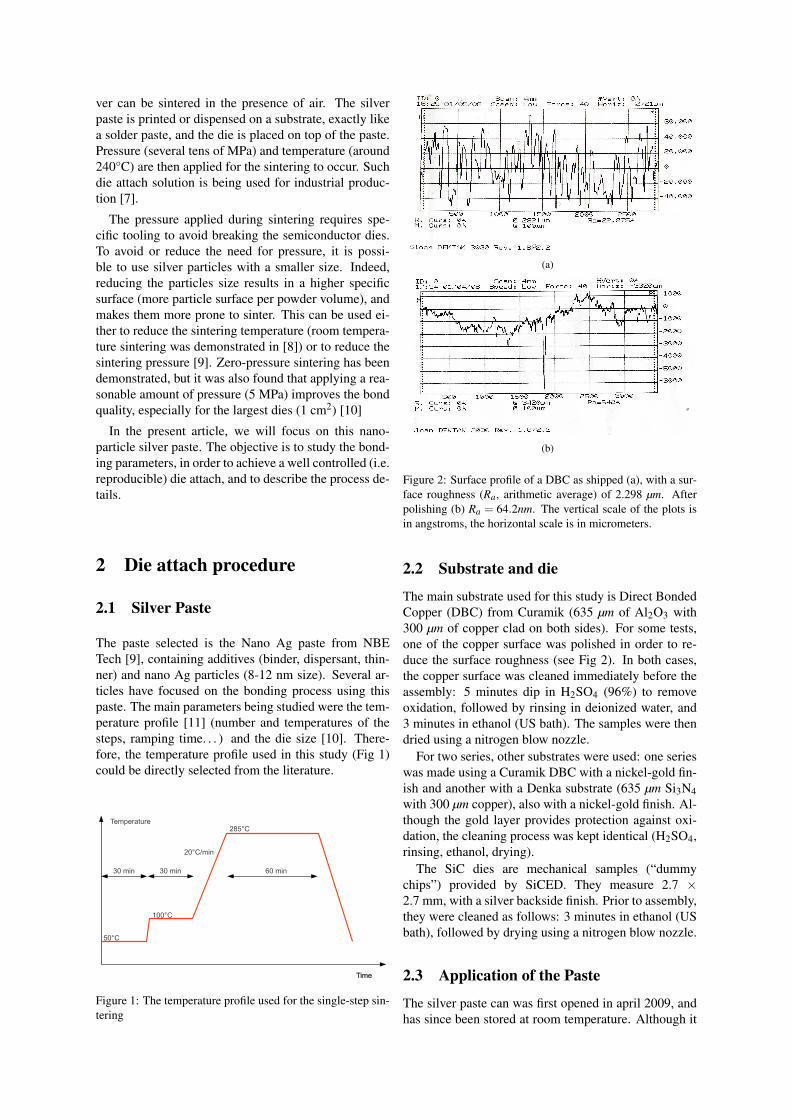
Figure 1: The temperature profile used for the single-step sin-
tering
(a)
(b)
Figure 2: Surface profile of a DBC as shipped (a), with a sur-
face roughness (Ra, arithmetic average) of 2.298 µm. After
polishing (b) Ra = 64.2nm. The vertical scale of the plots is
in angstroms, the horizontal scale is in micrometers.
2.2 Substrate and die
The main substrate used for this study is Direct Bonded
Copper (DBC) from Curamik (635 µm of Al2O3 with
300 µm of copper clad on both sides). For some tests,
one of the copper surface was polished in order to re-
duce the surface roughness (see Fig 2). In both cases,
the copper surface was cleaned immediately before the
assembly: 5 minutes dip in H2SO4 (96%) to remove
oxidation, followed by rinsing in deionized water, and
3 minutes in ethanol (US bath). The samples were then
dried using a nitrogen blow nozzle.
For two series, other substrates were used: one series
was made using a Curamik DBC with a nickel-gold fin-
ish and another with a Denka substrate (635 µm Si3N4
with 300 µm copper), also with a nickel-gold finish. Al-
though the gold layer provides protection against oxi-
dation, the cleaning process was kept identical (H2SO4,
rinsing, ethanol, drying).
The SiC dies are mechanical samples (“dummy
chips”) provided by SiCED. They measure 2.7 ×
2.7 mm, with a silver backside finish. Prior to assembly,
they were cleaned as follows: 3 minutes in ethanol (US
bath), followed by drying using a nitrogen blow nozzle.
2.3 Application of the Paste
The silver paste can was first opened in april 2009, and
has since been stored at room temperature. Although it
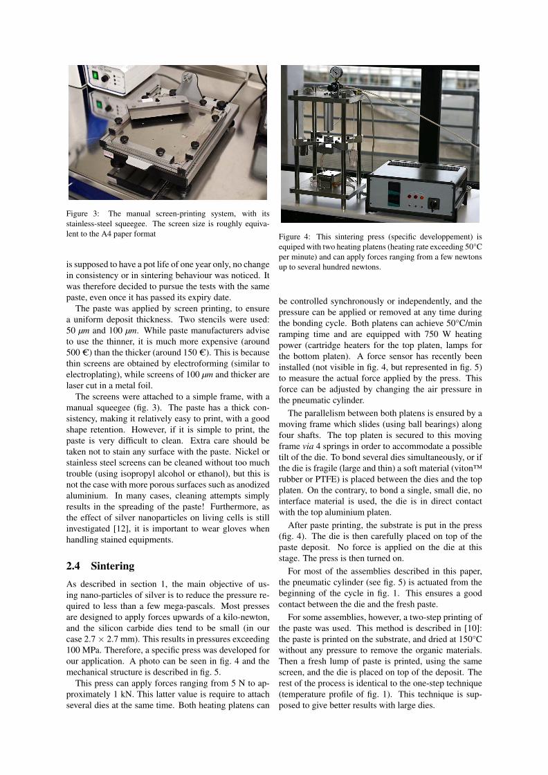
Figure 3: The manual screen-printing system, with its
stainless-steel squeegee. The screen size is roughly equiva-
lent to the A4 paper format
is supposed to have a pot life of one year only, no change
in consistency or in sintering behaviour was noticed. It
was therefore decided to pursue the tests with the same
paste, even once it has passed its expiry date.
The paste was applied by screen printing, to ensure
a uniform deposit thickness. Two stencils were used:
50 µm and 100 µm. While paste manufacturers advise
to use the thinner, it is much more expensive (around
500 C) than the thicker (around 150 C). This is because
thin screens are obtained by electroforming (similar to
electroplating), while screens of 100 µm and thicker are
laser cut in a metal foil.
The screens were attached to a simple frame, with a
manual squeegee (fig. 3). The paste has a thick con-
sistency, making it relatively easy to print, with a good
shape retention. However, if it is simple to print, the
paste is very difficult to clean. Extra care should be
taken not to stain any surface with the paste. Nickel or
stainless steel screens can be cleaned without too much
trouble (using isopropyl alcohol or ethanol), but this is
not the case with more porous surfaces such as anodized
aluminium. In many cases, cleaning attempts simply
results in the spreading of the paste! Furthermore, as
the effect of silver nanoparticles on living cells is still
investigated [12], it is important to wear gloves when
handling stained equipments.
2.4 Sintering
As described in section 1, the main objective of us-
ing nano-particles of silver is to reduce the pressure re-
quired to less than a few mega-pascals. Most presses
are designed to apply forces upwards of a kilo-newton,
and the silicon carbide dies tend to be small (in our
case 2.7 × 2.7 mm). This results in pressures exceeding
100 MPa. Therefore, a specific press was developed for
our application. A photo can be seen in fig. 4 and the
mechanical structure is described in fig. 5.
This press can apply forces ranging from 5 N to ap-
proximately 1 kN. This latter value is require to attach
several dies at the same time. Both heating platens can
Figure 4: This sintering press (specific developpement) is
equiped with two heating platens (heating rate exceeding 50°C
per minute) and can apply forces ranging from a few newtons
up to several hundred newtons.
be controlled synchronously or independently, and the
pressure can be applied or removed at any time during
the bonding cycle. Both platens can achieve 50°C/min
ramping time and are equipped with 750 W heating
power (cartridge heaters for the top platen, lamps for
the bottom platen). A force sensor has recently been
installed (not visible in fig. 4, but represented in fig. 5)
to measure the actual force applied by the press. This
force can be adjusted by changing the air pressure in
the pneumatic cylinder.
The parallelism between both platens is ensured by a
moving frame which slides (using ball bearings) along
four shafts. The top platen is secured to this moving
frame via 4 springs in order to accommodate a possible
tilt of the die. To bond several dies simultaneously, or if
the die is fragile (large and thin) a soft material (viton™
rubber or PTFE) is placed between the dies and the top
platen. On the contrary, to bond a single, small die, no
interface material is used, the die is in direct contact
with the top aluminium platen.
After paste printing, the substrate is put in the press
(fig. 4). The die is then carefully placed on top of the
paste deposit. No force is applied on the die at this
stage. The press is then turned on.
For most of the assemblies described in this paper,
the pneumatic cylinder (see fig. 5) is actuated from the
beginning of the cycle in fig. 1. This ensures a good
contact between the die and the fresh paste.
For some assemblies, however, a two-step printing of
the paste was used. This method is described in [10]:
the paste is printed on the substrate, and dried at 150°C
without any pressure to remove the organic materials.
Then a fresh lump of paste is printed, using the same
screen, and the die is placed on top of the deposit. The
rest of the process is identical to the one-step technique
(temperature profile of fig. 1). This technique is sup-
posed to give better results with large dies.
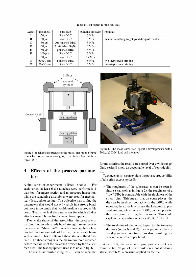
Table 1: Test matrix for the SiC dies
Series thickness substrate bonding pressure remarks
A’ 50 µm Raw DBC 6 MPa
B 50 µm Raw DBC 6 MPa manual scrubbing to get good die-paste contact
C 50 µm Au-finished DBC 6 MPa
D 50 µm Au-finished Si3N4 6 MPa
E 50 µm polished DBC 6 MPa
F 100 µm Raw DBC 6 MPa
J 50 µm Raw DBC 0.7 MPa
N 50+50 µm polished DBC 6 MPa two-step screen printing
O 50+50 µm Raw DBC 6 MPa two-step screen printing
Figure 5: mechanical structure of the press. The mobile frame
is attached to two counterweights, to achieve a low minimal
force (<5 N).
3 Effects of the process parame-
ters
A first series of experiments is listed in table 1. For
each series, at least 6 die attaches were performed: 1
was kept for micro-section and microscope inspection,
while the remaining assemblies were used for mechan-
ical (destructive) testing. The objective was to find the
parameters that would not only result in a strong bond,
but more importantly that would result in a reproducible
bond. That is, to find the parameters for which all dies
attaches would break for the same force applied.
Due to the shape of the assemblies, the most practi-
cal (and commonly used) bond strength assessment is
the so-called “shear test” in which a tool applies a hor-
izontal force on one side of the die, the substrate being
kept secured. This results in a shear stress in the die at-
tach. The shear strength is the maximum force recorded
before the failure of the die attach divided by the die sur-
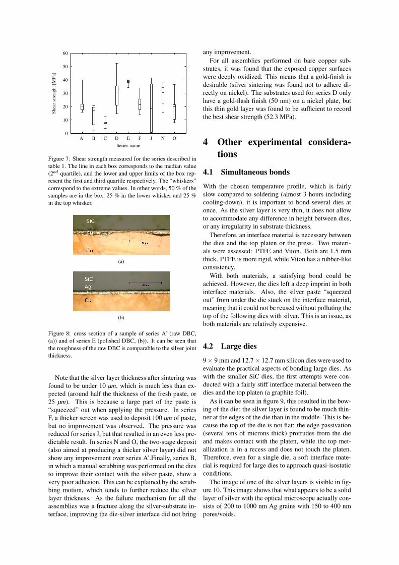
face area. The test equipment used is visible in fig. 6.
The results are visible in figure 7. It can be seen that
Figure 6: The shear tester used (specific development), with a
20 kgf (200 N) load cell mounted
for most series, the results are spread over a wide range.
Only series E show an acceptable level of reproducibil-
ity.
Two mechanisms can explain the poor reproducibility
of all series except series E:
• The roughness of the substrate: as can be seen in
figure 8 (as well as in figure 2), the roughness of a
“raw” DBC is comparable with the thickness of the
silver joint. This means that on some places, the
die can be in direct contact with the DBC, while
on other, the silver layer is not thick enough to pre-
vent voiding. On a polished DBC, on the opposite,
the silver joint is of regular thickness. This could
explain the spreading of series A’, B, C, D, F, J
• The oxidation of the copper layer: for the two-step
deposits (series N and O), the copper under the sil-
ver deposit has more time to oxidize, resulting in a
weaker silver-to-copper bond.
As a result, the most satisfying parameter set was
found to be: 50 µm of silver paste on a polished sub-
strate, with 6 MPa pressure applied on the die.
0
10
20
30
40
50
60
A’ B C D E F J N O
Shea
r st
renght
[MP
a]
Series name
Figure 7: Shear strength measured for the series described in
table 1. The line in each box corresponds to the median value
(2nd quartile), and the lower and upper limits of the box rep-
resent the first and third quartile respectively. The “whiskers”
correspond to the extreme values. In other words, 50 % of the
samples are in the box, 25 % in the lower whisker and 25 %
in the top whisker.
(a)
(b)
Figure 8: cross section of a sample of series A’ (raw DBC,
(a)) and of series E (polished DBC, (b)). It can be seen that
the roughness of the raw DBC is comparable to the silver joint
thickness.
Note that the silver layer thickness after sintering was
found to be under 10 µm, which is much less than ex-
pected (around half the thickness of the fresh paste, or
25 µm). This is because a large part of the paste is
“squeezed” out when applying the pressure. In series
F, a thicker screen was used to deposit 100 µm of paste,
but no improvement was observed. The pressure was
reduced for series J, but that resulted in an even less pre-
dictable result. In series N and O, the two-stage deposit
(also aimed at producing a thicker silver layer) did not
show any improvement over series A’.Finally, series B,
in which a manual scrubbing was performed on the dies
to improve their contact with the silver paste, show a
very poor adhesion. This can be explained by the scrub-
bing motion, which tends to further reduce the silver
layer thickness. As the failure mechanism for all the
assemblies was a fracture along the silver-substrate in-
terface, improving the die-silver interface did not bring
any improvement.
For all assemblies performed on bare copper sub-
strates, it was found that the exposed copper surfaces
were deeply oxidized. This means that a gold-finish is
desirable (silver sintering was found not to adhere di-
rectly on nickel). The substrates used for series D only
have a gold-flash finish (50 nm) on a nickel plate, but
this thin gold layer was found to be sufficient to record
the best shear strength (52.3 MPa).
4 Other experimental considera-
tions
4.1 Simultaneous bonds
With the chosen temperature profile, which is fairly
slow compared to soldering (almost 3 hours including
cooling-down), it is important to bond several dies at
once. As the silver layer is very thin, it does not allow
to accommodate any difference in height between dies,
or any irregularity in substrate thickness.
Therefore, an interface material is necessary between
the dies and the top platen or the press. Two materi-
als were assessed: PTFE and Viton. Both are 1.5 mm
thick. PTFE is more rigid, while Viton has a rubber-like
consistency.
With both materials, a satisfying bond could be
achieved. However, the dies left a deep imprint in both
interface materials. Also, the silver paste “squeezed
out” from under the die stuck on the interface material,
meaning that it could not be reused without polluting the
top of the following dies with silver. This is an issue, as
both materials are relatively expensive.
4.2 Large dies
9 × 9 mm and 12.7 × 12.7 mm silicon dies were used to
evaluate the practical aspects of bonding large dies. As
with the smaller SiC dies, the first attempts were con-
ducted with a fairly stiff interface material between the
dies and the top platen (a graphite foil).
As it can be seen in figure 9, this resulted in the bow-
ing of the die: the silver layer is found to be much thin-
ner at the edges of the die than in the middle. This is be-
cause the top of the die is not flat: the edge passivation
(several tens of microns thick) protrudes from the die
and makes contact with the platen, while the top met-
allization is in a recess and does not touch the platen.
Therefore, even for a single die, a soft interface mate-
rial is required for large dies to approach quasi-isostatic
conditions.
The image of one of the silver layers is visible in fig-
ure 10. This image shows that what appears to be a solid
layer of silver with the optical microscope actually con-
sists of 200 to 1000 nm Ag grains with 150 to 400 nm
pores/voids.
(a)
(b)
Figure 9: cross section of the die attach of a 9 mm Si die at
the edge (a) and in the middle (b).
5 Conclusion
The implementation of a silver-sintering based solution
for die attach has been described. Although this tech-
nology does not require very complex equipments (the
process takes place in air, with moderate temperature
and pressure), some precautions must be taken to en-
sure good results.
In particular, it was shown that the roughness of
the substrate has a very significant effect on the re-
producibility of the die attach. Other effects, such as
substrate finish or the thickness of the paste deposit,
are not as obvious. In particular, further experiments
are needed to reduce the pressure required and achieve
thicker silver joints.
Acknowledgments
The authors would like to thank the “Fondation pourla Recherche en Aéronautique et Espace” (FRAE)its financial support of this work, under grant name“EPAHT”
References
[1] V. Manikam and K. Y. Cheong, “Die Attach Materials
for High Temperature Applications: A Review,” Compo-
nents, Packaging and Manufacturing Technology, IEEE
Transactions on, vol. 1, no. 4, pp. 457 –478, april 2011.
[2] K. Guth, D. Siepe, J. Görlich, H. Torwesten, R. Roth,
F. Hille, and F. Umbach, “New assembly and inter-
Figure 10: FIB ion channelling contrast image of a silver joint
between a Si die and an DBC substrate (FIB micro-section)
connects beyond sintering methods,” in Proceedings of
PCIM, Nuremberg, may 2010, pp. 232–237.
[3] B. McPherson, J. M. Hornberger, J. Bourne, A. B.
Lostetter, R. M. Schupbach, R. Shaw, B. Reese, B. Row-
den, H. A. Mantooth, S. Ang, J. C. Balda, K. Okumura,
and T. Otsuka, “Packaging of High Temperature 50kW
SiC Motor Drive Module for Hybrid-Electric Vehicles,”
Advancing Microelectronics, vol. 37, no. 1, pp. 20–26,
jan 2010.
[4] P. O. Quintero, T. Oberc, and F. P. McCluskey, “High
Temperature Die Attach by Transient Liquid Phase Sin-
tering,” in HiTEC 2008. Albuquerque: IMAPS, may
2008, pp. 207–212.
[5] H. Schwarzbauer, “Method of securing electronic
components to a substrate.” U.S Patent Patent 4 810 672,
mar 7, 1989. [Online]. Available: http://www.google.
com/patents/about?id=ViVhAAAAEBAJ&dq=4810672
[6] H. Schwarzbauer and R. Kuhnert, “Novel large area
joining technique for improved power device perfor-
mance,” Industry Applications, IEEE Transactions on,
vol. 27, no. 1, pp. 93 –95, jan. 1991.
[7] C. Göbl, P. Beckedahl, and H. Braml, “Low temper-
ature sinter technology Die attachment for automotive
power electronic applications,” in Automotive Power
Electronics, Paris, 21–22 jun 2006, p. 5. [Online]. Avail-
able: www.semikron.com/internet/webcms/objects/pdf/
APE2006_Goebl.pdf
[8] D. Wakuda, K.-S. Kim, and K. Suganuma, “Ag
Nanoparticle Paste Synthesis for Room Temperature
Bonding,” IEEE Transaction on Components and Pack-
aging Technology, vol. 33, no. 1, pp. 1–6, mar 2010.
[9] G. Bai, “Low-Temperature Sintering of Nanoscale
Silver Paste for Semiconductor Device Intercon-
nection,” Ph.D. dissertation, Virginia Polytechnic
Institute and State University, Blacksburg, Virginia,
oct 2005. [Online]. Available: http://scholar.lib.vt.edu/
theses/available/etd-10312005-163634/unrestricted/
Dissertation-GBai05.pdf

[10] T. G. Lei, J. N. Calata, G.-Q. Lu, X. Chen, and S. Luo,
“Low-Temperature Sintering of Nanoscale Silver Paste
for Attaching Large-Area (>100mm2) Chips,” IEEE
Transaction on Components and Packaging Technology,
vol. 33, no. 1, pp. 98–104, mar 2010.
[11] T. Wang, X. Chen, G.-Q. Lu, and G.-Y. Lei, “Low-
Temperature Sintering with Nano-Silver Paste in Die-
Attached Interconnection,” journal of electronic materi-
als, vol. 36, no. 10, pp. 1333–1340, 2007.
[12] N. Lubick, “Nanosilver toxicity: ions, nanoparticles or
both?” Environmental Science & Technology, vol. 42,
no. 23, pp. 8617–8617, 2008. [Online]. Available:
http://pubs.acs.org/doi/abs/10.1021/es8026314


![LOW-TEMPERATURE SINTERING AND MICROWAVE DIELECTRIC ...€¦ · and promotes the densification by liquid phase sintering [12-14]. However, over sintering would cause abnormal grain](https://static.fdocuments.in/doc/165x107/5fb3b4a9e5540561916e2940/low-temperature-sintering-and-microwave-dielectric-and-promotes-the-densification.jpg)


