DHX91 DHAN Module Datasheet - DSP Group 1.3 DHX91 DHAN Module Datasheet Table of Contents June 2015...
18
DHX91 DHAN Module DECT-ULE Platform Datasheet Version 1.3 June 2015
Transcript of DHX91 DHAN Module Datasheet - DSP Group 1.3 DHX91 DHAN Module Datasheet Table of Contents June 2015...

DHX91 DHAN Module DECT-ULE Platform
Datasheet
Version 1.3
June 2015

Version 1.3 DHX91 DHAN Module Datasheet Worldwide Sites
June 2015 DSP Group Confidential 2/18
Headquarters
USA DSP Group Inc.
161 S San Antonio Rd
Suite 10 Los Altos, CA 94022
Tel: (408)986-4300
Fax:(408)986-4323
Israel
DSP Group Ltd. 5 Shenkar Street
Herzelia, Israel 4672505 Tel: 972-9-952-9696
Fax: 972-9-954-1234
Europe
Germany
DSPG Technologies GmbH Nelson-Mandela-Platz 18
90459 Nurnberg
Tel: +49-911-2001-0 Fax: +49-911-2001-1210
Scotland DSPG Edinburgh Ltd.
Geddes House
Kirkton North Livingston EH54 6GU
Tel: +44-(0)1506-407-730
APAC
China DSP Group (HK) Limited
Unit 1-4, 11/F,
909 Cheung Sha Wan Rd. Kowloon
Hong Kong
Tel: +852-(3965)-5888
DSP Group (Shenzhen) Limited
Room 1819, 18/F Kerry Centre, Renminnan Road,
Shenzhen, China 518001 Tel: +(86 755) 2518 1214
Ascend Technology Inc.
Room 1303,
New World Center,
No.6009 Yitian Road, Futian District,
Shenzhen City, China
Tel: +86-755-820-24598 Fax: +86-755-239-82986
Ascend Technology Inc. Rm 607,
Hui Huang International Center,
1st Place, Shangdi 10th Road, Haidian District, Beijing City, P.R.
Japan
DSP Group (Japan) Inc. 1-29-1 Nishi-Gotanda
Shinagawa-Ku Tokyo 141-0031
Tel:+81-(3)-3493-3050
Tomen Electronics
8-27, Kohnan 1 Chome, Minato-ku, Tokyo
108-8510, Japan
Tel: +81-(3)-5462-9619 Fax: +81-(3)-5462-9686
Korea
Daesung Semiconductors
140-848, RM 401
Wonhyo BD. 46-1
Wonhyo-ro 3ka, Yongsan-gu,
Seoul, Korea Tel: +82-(2)-3272-7300
Fax: +82-(2)-712-4632-3
India
DSP Technology Indian Private
Limited Information Technology Park
Nagawara Village Kasaba Hobli
Bangalore 560045 Tel: +91 80 4024 8399
Taiwan Ascendtek Electronics, Inc
11F-7, No. 77, Sec. 1
Hsin Tai Wu Rd., Hsi Chih
Taipei Hsien,
Taiwan, R.O.C Tel: 886-2-2698-8696
Fax: 886-2-8698-2138
This document is provided by DSP Group, Inc. and/or one or more of its subsidiaries (“DSP Group”). All information and data contained in this document is for informational purposes only, without any commitment on the part of DSP Group, and is not to be considered as
an offer for a contract. DSP Group shall not be liable, in any event, for any claims for damages or any other remedy in any jurisdiction
whatsoever, whether in an action in contract, tort (including negligence and strict liability) or any other theory of liability, whether in law or equity including, without limitation, claims for damages or any other remedy in whatever jurisdiction, and shall not assume
responsibility for patent infringements or other rights to third parties, arising out of or in connection with this document. Further, DSP
Group reserves the right to revise this publication and to make changes to its content, at any time, without obligation to notify any person or entity of such revision changes. These materials are copyrighted and any unauthorized use of these materials may violate copyright,
trademark, and other laws. Therefore, no part of this publication may be reproduced, photocopied, stored on a retrieval system, or
transmitted without the express written consent of DSP Group. Any new issue of this document invalidates previous issues.
DSP Group reserves the right to revise this publication and to make changes to its content, at any time, without obligation to notify any
person or entity of such revision changes.
© 2015 DSP Group Confidential. All rights reserved.

Version 1.3 DHX91 DHAN Module Datasheet Table of Contents
June 2015 DSP Group Confidential 3/18
TABLE OF CONTENTS
1. INTRODUCTION ........................................................................................................................................... 4
1.1. General Description ................................................................................................................................. 4 1.2. Block Diagram ......................................................................................................................................... 4 1.3. Features .................................................................................................................................................... 5
2. PIN AND SIGNAL DESCRIPTION ............................................................................................................... 6
2.1. Pin List ..................................................................................................................................................... 6
3. MODULE ELECTRICAL SPECIFICATIONS .............................................................................................. 8
3.1. Absolute Maximum Rating ...................................................................................................................... 8 3.2. Recommended Operating Conditions ...................................................................................................... 8 3.3. Power Consumption................................................................................................................................. 9 3.4. Transmitter............................................................................................................................................. 10 3.5. Receiver ................................................................................................................................................. 10
4. MODIFYING MODULE SOFTWARE AND ADJUSTING PARAMETERS ............................................ 11
5. APPLICATION SCHEMATIC GUIDE ........................................................................................................ 11
5.1. Power Supply and Battery Check .......................................................................................................... 11 5.2. UART Interface and Wakeup (Applications running on external MCU) .............................................. 12 5.3. Driving LEDs ........................................................................................................................................ 13 5.4. DHAN Standalone Applications ............................................................................................................ 13
6. APPLICATION PCB DESIGN RECOMMENDATIONS ............................................................................ 14
6.1. Antenna Recommendations ................................................................................................................... 14
6.1.1. Wire Antennas ................................................................................................................................ 14 6.1.2. Chip Antennas ................................................................................................................................. 15 6.1.3. Printed Antennas ............................................................................................................................. 15
7. ASSEMBLY INFORMATION ..................................................................................................................... 16
7.1. Mechanical............................................................................................................................................. 16 7.2. Surface Mount ....................................................................................................................................... 16
8. SUPPLEMENTARY INFORMATION ........................................................................................................ 17
8.1. Ordering Information ............................................................................................................................. 17 8.2. Abbreviations Used ............................................................................................................................... 17 8.3. Change Log............................................................................................................................................ 17
LIST OF FIGURES ............................................................................................................................................... 18
LIST OF TABLES ................................................................................................................................................ 18

Version 1.3 DHX91 DHAN Module Datasheet Introduction
June 2015 DSP Group Confidential 4/18
1. Introduction
1.1. General Description
The DSPG DHAN module is based on the state-of-the-art DHX91 - a 4th
generation DECT SOC. The DHAN
module is appropriate for the AC or battery powered ULE Node operating in a star network with a ULE-
certified Controller at the hub.
The DHAN is a “turn-key” solution providing the user with a jump-start in developing a ULE Node
Application. It is easily integrated into the smallest of ULE Nodes, providing excellent range with minimized
drain on the battery, allowing the designer to focus on developing the application. The complete platform
includes an SDK, API GUI, and user documentation.
The DHAN module can be used as a standalone solution (with the application running on the DHX91 ARM)
or it can provide the wireless connectivity channel for a sensor application running on an external MCU. In
the latter case, the MCU communicates with the DHAN via serial UART interface.
For the standalone DHAN case (or other cases where customization is required), the user will need to account
for replacing the standard HAN-FUN SW stack with a customized stack
1.2. Block Diagram
DHAN
Antenna
Matching,
external
to
Module
JTAG
I2C
GPIO
VCC
DHX91QSPI
13M
XTAL
ULE IO
ULE ADC/DAC
UART
Figure 1-1: DXH91 DHAN Module Block Diagram

Version 1.3 DHX91 DHAN Module Datasheet Introduction
June 2015 DSP Group Confidential 5/18
1.3. Features
General
Appropriate for both battery
powered and AC-powered ULE
Nodes
Includes embedded HAN-FUN
ULE SW Stack with well-
documented API for control via
external application MCU
Processor (ARM926 32-bit RISC
Controller) and memory
appropriate for standalone DHAN
solutions (requires SW
customization)
Best-in-class radio performance
Tx power: +23.5 dBm
Rx sensitivity: -96
dBm@1000 ppm
Hibernation mode: low power (<2
uA)
Support for EU, US and other
regional DECT bands
Compliance with EN301406, FCC
part 15.329 & ARIB STD-T101
Small form factor: 15 mm x 32.5
mm x 3.8 mm
Low external BOM
Well matched RF Port, easily
connected to an off-module 50-
Ohm antenna
Operating temperature: -40° C to
+85° C
Applications
Home automation
Home security
Connected appliances
Smart energy

Version 1.3
DHX91 DHAN Module Datasheet Pin and Signal Description
June 2015 DSP Group Confidential 6/18
2. Pin and Signal Description
2.1. Pin List
Table 2-1: DHAN Module Pinout
PIN NO. NAME DESCRIPTION/TYPE
1 GND GND
2 DCINS NC (Not Connected)
3 DCIN3 Used to monitor battery level via this ADC input.
4
RSTN
Pull to GND to force reset. Optionally connect to
external MCU output or to a SPST switch (for
manual reset) or leave NC
5 SCL
I2C Clock I/O. Not used by HAN_FUN. Can be left
as NC
6 SDA
I2C Data I/O, Not used by HAN_FUN. Can be left as
NC
7 IIC_ACK
I2C ACK, Not used by HAN_FUN. Can be left as
NC
8 GPIO7 General Purpose I/O. Can be left NC
9 GPIO8 General Purpose I/O. Can be left NC
10 RxD (GPIO9) UART Rx
11 TDI JTAG Data In, If not needed, can be left NC
12 TMS JTAG Mode Select, If not needed, can be left NC
13 TDO JTAG Data Out, If not needed, can be left NC
14 TCK JTAG Clock, If not needed, can be left NC
15 RTCK JTAG Reset, If not needed, can be left NC
16-17 GND GND
18 TxD (GPIO10) UART Tx
19 VDD_APU 1.8V test point. 0V during hibernate. Leave NC
20 VDD 1.2V test point. 0V during hibernate. Leave NC
21 VCC
Power Supply Input. Connect to Battery or 3V
regulated supply
22 DOUBCAP2P ULE I/O. If not used, can be left NC
23 DCIN2 ULE I/O. If not used, can be left NC
24 VCC3V 3V test point. 0V during hibernate. Leave NC
25 LEDSINK/DCIN ULE I/O. If not used, can be left NC
26-27 GND GND

Version 1.3
DHX91 DHAN Module Datasheet Pin and Signal Description
June 2015 DSP Group Confidential 7/18
PIN NO. NAME DESCRIPTION/TYPE
28 AMP2_OUT ULE I/O. If not used, can be left NC
29 AMP1_P ULE non-inverting sensor conditioning input
30 AMP1_OUT ULE I/O. If not used, can be left NC
31 MPWR/ANA2_IN
ULE I/O (or Microphone Power). If not used, can be
left NC
32 MIN Leave NC
33 MIP Leave NC
34 ANA_IN1 ULE I/O. If not used, can be left NC
35 SPOUTP Leave NC
36 SPOUTN Leave NC
37 PWM0 Analog Output
38 XIN_32K Leave NC
39 XOUT_32K Leave NC
40 VDD_ULE 1.8V test point. Active during hibernate. Leave NC
41 VCCRF Power Supply Input to RF
42-50 GND GND
51 Antenna RF In/Out, 50 Ohm
52 GND GND

Version 1.3 DHX91 DHAN Module Datasheet Module Electrical Specifications
June 2015 DSP Group Confidential 8/18
3. Module Electrical Specifications
All parameters are for 25ºC.
3.1. Absolute Maximum Rating
Table 3-1: Absolute Maximum Rating
PIN NAME PIN MIN MAX UNIT
VCC 21 -0.3 4.6 V
VccRF 41 -0.3 4.6 V
I2C 5, 6, 7 -0.3 4.6 V
JTAG 11, 12, 13, 14, 15 -0.3 4.6 V
GPIO 8, 9, 10, 18 -0.3 4.6 V
DCINs,DCIN1,2,3 2, 3, 23, 25 -0.3 4.6 V
Storage Temperature - -45 +90 °C
3.2. Recommended Operating Conditions
Table 3-2: Recommended Operating Conditions
RATING CONDITIONS MIN TYP MAX UNIT
Operating ambient
temperature
-40 +25 +85 °C
VccRF, VCC 1.95 3.0 3.6 V
JTAG, UART
VIL
VIH
VOL
VOH
(VCC is at
nominal 3V)
2.0
2.4
0.8
0.4
V
DCIN3 1.95 3.0 VCC V

Version 1.3 DHX91 DHAN Module Datasheet Module Electrical Specifications
June 2015 DSP Group Confidential 9/18
3.3. Power Consumption
Table 3-3: Power Consumption
PARAMETER TEST CONDITIONS TYP MAX UNIT
Tx Current VccRF=3 V
VCC=3 V
Band=EU @ 23dBm
400 480 mA
Tx Current VccRF=3 V
VCC=3 V
Band=US @ 21 dBm
250 300 mA
Rx Current VccRF=3 V
VCC=3 V
125 135 mA
Hibernation VccRF=3 V
VCC=3 V
1.7 2.5 uA

Version 1.3 DHX91 DHAN Module Datasheet Module Electrical Specifications
June 2015 DSP Group Confidential 10/18
3.4. Transmitter
Table 3-4: Tx Characteristics
CHARACTERISTICS TEST CONDITIONS MIN TYP MAX UNIT
NTP VccRF=3 V
VCC=3 V
Band=EU
22 23 24 dBm
NTP VccRF=3 V
VCC=3 V
Band=US
19 20 21 dBm
Harmonics VccRF=3 V
VCC=3 V
Band=EU & US
-40 -35 dBm
Transmission Mask EN 301406
Paragraph 5.3.3
Comply N/A
Frequency Offset EN 301406
Paragraph 5.3.1
-50 8 +50 KHz
Frequency Drift EN 301406
Paragraph 5.3.5
-15 0 +15 KHz/Slot
Emission Due
Modulation
EN 301406
Paragraph 5.3.6.2
M±1
M±2
M±3
M>±3
-20
-42
-47
-50
-8
-30
-40
-44
dBm
3.5. Receiver
Table 3-5: Rx Characteristics
CHARACTERISTICS TEST CONDITIONS MIN TYP MAX UNIT
Sensitivity, BER <
1000ppm
VccRF=3 V
VCC=3 V
-96 -93 dBm
Maximum input power VccRF=3 V
VCC=3 V
15 dBm

Version 1.3 DHX91 DHAN Module Datasheet Application Information
June 2015 DSP Group Confidential 11/18
4. Modifying Module Software and Adjusting Parameters
The DHAN module is loaded with the standard HAN-FUN image, configured for application control by an
external MCU via the UART CMND Node Interface. It is also configured for European band operation, with
a generic ID (IPEI in DECT nomenclature) and it will identify itself as a smoke detector. These latter 3 items
are configurable ULE parameters that can be modified by the user and stored back into the module non-
volatile memory. However, if the user application is using the DHX91 as a standalone controller (ie no
external MCU) or needs some means other than the UART CMND interface for communication between the
external MCU and the DHAN – customization and reloading of the software image running on the DHAN is
required.
Custom software images as well as ULE parameters can be updated either via the JTAG or the UART I/F.
DSP Group can supply a tool (Vega Memory Tool) to accomplish both image update and parameter
modification using the JTAG I/F. So it is recommended that the customer include test points in the application
board layout to access the JTAG port (see schematic tips later on) – at least during development phase. Note,
however, that this tool, while appropriate for prototype needs, is likely not suitable for a mass production
setting – in particular if a new image needs to be burned.
The UART CMND API includes commands for updating parameters. Furthermore, the UART I/F can
facilitate more efficient means of erasing and refreshing the software image on the DHAN. So the user should
consider exposing this I/F as well for connecting to his production rack. If the application board includes an
external MCU, than its UART I/F will need to be tri-stated during this production phase.
5. Application Schematic Guide
This section describes how to connect the DHAN to the power supply, to an external MCU via UART and to
LED indicators
5.1. Power Supply and Battery Check
DHAN
VCC (21)
VCCRF (41)
DCIN3 (3)
GND (1,16,17,26,27, 42-50, 52)
Battery or Regulator Output
Bulk Cap*
Notes:
1) Bulk cap is not required when using lithium batteries such CR123A or CR2. Suggest 100µF cap for AA
or AAA applications and 500mF for CR2032 Coin-Cell operation
2) DCIN3 is an input to an ADC that monitors the battery level
Figure 5-1: Power Supply and Battery Detect Interconnect

Version 1.3 DHX91 DHAN Module Datasheet Application Information
June 2015 DSP Group Confidential 12/18
5.2. UART Interface and Wakeup (Applications running on external MCU)
In circumstances where the external MCU detects an event that needs to be communicated to the DHAN, it
will need to wake up the DHAN from its low current hibernation mode, wait ~10mS for the DHX91 to reboot
and then signal to the DHX91 via UART I/F. There are two options for the external MCU to wake the DHAN
from hibernation:
1) Apply a rising edge to one of the ULE I/O (configured as a Digital Wakeup), wait ~10mS and begin
communication with the DHX91 DHAN via UART. See Figure 5-2
2) Begin communication via UART, with the expectation that it will take ~10mS for the ext MCU to obtain
a response from the awaking DHAN. See Figure 5-3
In other circumstances, an incoming Page or Alert from the Controller will be detected by the DHAN. If the
external MCU is in a Sleep Mode the DHAN will need to first awake the MCU. Most MCUs will wake upon
sensing transitions on the DHAN UART TxD line. However, some may require (prefer) to be woken up by
application of a rising edge to a generic digital input at the MCU. This option is also called out in Figure 5-2.
DHAN
GPIO9/RxD(10)
GPIO10/TxD (18)
ULE_IO*
ULE_IO or GPIO
Ext MCU
Wakeup
Wakeup
RxD
TxD
Note: ULE IOs are pins 22, 25, 28, 30, 31, 34
Figure 5-2: UART I/F with bi-directional, dedicated signals for wakeup
Ext MCUPin34
DHAN
Pin30
Pin10
Pin18
TxD
TxD
RxD
Figure 5-3: UART I/F used for wakeup of DHAN

Version 1.3 DHX91 DHAN Module Datasheet Application Information
June 2015 DSP Group Confidential 13/18
5.3. Driving LEDs
LEDs that need to operate while the DHAN is in hibernation can utilize the ANA_IN1 pin (34) which can be
configured as a PWM and the LEDSINK pin (25) which features a PWM with LED sink capabilities. For
DHAN active or registration indications, PWM0 (pin37) can also be used.
5.4. DHAN Standalone Applications
The DHX91 ULE block includes a Sensor Conditioning Module which can facilitate many types of ULE
applications. This module is a highly configurable analog circuit that can be used to interface to a wide
variety of sensor transducers.
The module is built around the following sub-circuits:
Two analog operational amplifiers (op-Amps) with shared bias source
Two analog comparators with digital output
One configurable digital potentiometer
Three configurable ratiometric voltage references with selectable source
Several analog distribution MUXes
Several sample-and-hold (S&H) mechanisms
Version 1.3 DHX91 DHAN Module Datasheet Application Information
June 2015 DSP Group Confidential 14/18
6. Application PCB Design Recommendations
It is recommended that unused pads on the Application PCB not be left as isolated islands of copper but rather
be anchored with via to inner layers of the PCB. It is also recommend that GND vias be applied liberally in
the vicinity of the antenna pin output (Pin 51) and the associated GND pins (42-50 and 52).
The following layout recommendations need to be apply on Main Board:
1. Implement a solid ground under the DHAN module.
2. Do not route signal traces under the module. Use the bottom layer for signal routing.
3. Make sure no components are near the antenna.
4. Locate the antenna on the edge of the PCB.
5. Use coplanar wave-guide trace between the DHAN module and antenna, it should be designed to be as
short as possible with 50Ω impedance.
6. Add GND vias alongside the RF trace.
7. Route the RF trace with gradual bends and no sharp corners.
8. Design the antenna position according to the common usage/position of the ULE product for optimal
range.
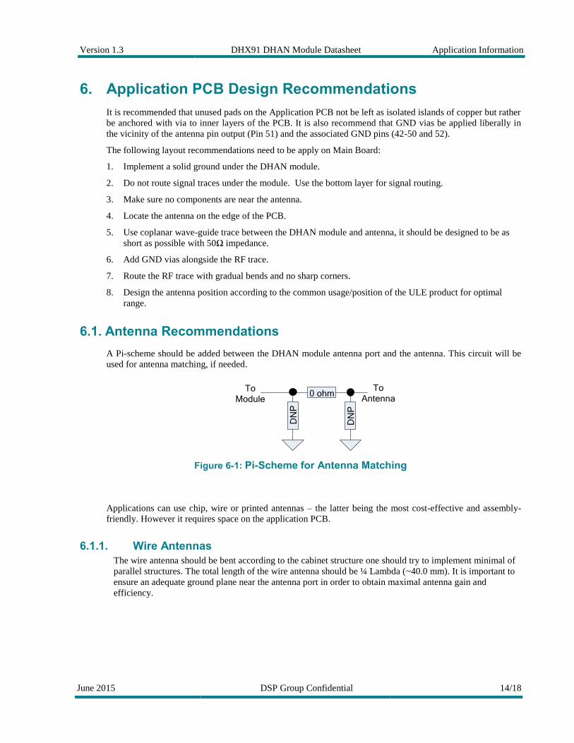
6.1. Antenna Recommendations
A Pi-scheme should be added between the DHAN module antenna port and the antenna. This circuit will be
used for antenna matching, if needed.
To
Module
To
Antenna
DN
P
DN
P
0 ohm
Figure 6-1: Pi-Scheme for Antenna Matching
Applications can use chip, wire or printed antennas – the latter being the most cost-effective and assembly-
friendly. However it requires space on the application PCB.
6.1.1. Wire Antennas
The wire antenna should be bent according to the cabinet structure one should try to implement minimal of
parallel structures. The total length of the wire antenna should be ¼ Lambda (~40.0 mm). It is important to
ensure an adequate ground plane near the antenna port in order to obtain maximal antenna gain and
efficiency.

Version 1.3 DHX91 DHAN Module Datasheet Application Information
June 2015 DSP Group Confidential 15/18
6.1.2. Chip Antennas
P/N Manufacture
ANT8868LL00R1880A Yageo
CAN4311112001881K Yageo
W3022 Pulse Elect
6.1.3. Printed Antennas
The most popular are INV-F-Antenna and monopole antenna, RF CAD tools are recommended to use when
designing such, below one can find typical INV-F-Antenna dimensions for DECT band.
1060 mil
85 mil
18
0 m
il
25
mil
GN
D
Fe
ed
ing
Po
int
Figure 6-2: INV-F-Antenna Dimension
A practical, more compact version of this inverted-F is shown below. Contact DSPG to obtain the design file.

Version 1.3 DHX91 DHAN Module Datasheet Application Information
June 2015 DSP Group Confidential 16/18
7. Assembly Information
7.1. Mechanical
Pin
-42
Pin
-1
Pin
-16
Pin-17
13.0214.5015.77
1.59
Typ 1.27
3.72
0.90
31.45
32.55
2.60P
in-2
7
Pin-26
Pin-51 Antenna
Shield
Figure 7-1: Module Mechanical Outline
Figure 7-2: Recommended PCB Footprint
7.2. Surface Mount
The DHAN module uses a flat shield cover for a fully automatic assembly process. For backing and reflow
recommendations, use MSL 3 in the JEDEC/IPC standard J-STD-20b. The temperature classification (TC) for
the module is 245° C.

Version 1.3 DHX91 DHAN Module Datasheet Supplementary Information
June 2015 DSP Group Confidential 17/18
8. Supplementary Information
8.1. Ordering Information
Part #: DHX91MDMCFAE5AMI
8.2. Abbreviations Used
Table 8-1: Abbreviations
ACRONYM DESCRIPTION
GPIO General-Purpose Input Output
I2C Inter Integrated Circuit
JTAG Joint Test Action Group, the common name for the IEEE
1149.1 standard test access port and boundary-scan
architecture
RF Radio Frequency
UART Universal Asynchronous Receiver Transmitter
ULE Ultra Low Energy
8.3. Change Log
Table 8-2: List of Changes
REVISION DATE DESCRIPTION
1.0 July 2014 First release
1.1 December 2014 Corrected App Schematic
1.2 February 2015
*Clarified that printed antenna is not
incorporated in the module.
*Added recommendations for application
board PCB
1.3 June 2015
*Add Application Schematic and Layout
*Add PCB footprint
*Corrected Part# in Ordering Info

Version 1.3 DHX91 DHAN Module Datasheet List of Tables
June 2015 DSP Group Confidential 18/18
LIST OF FIGURES
Figure 1-1: DXH91 DHAN Module Block Diagram .................................................................................................... 4
Figure 5-1: Power Supply and Battery Detect Interconnect ........................................................................................ 11
Figure 5-2: UART I/F with bi-directional, dedicated signals for wakeup ................................................................... 12
Figure 5-3: UART I/F used for wakeup of DHAN ...................................................................................................... 12
Figure 6-1: Pi-Scheme for Antenna Matching ............................................................................................................. 14
Figure 6-2: INV-F-Antenna Dimension ...................................................................................................................... 15
Figure 7-1: Module Mechanical Outline ..................................................................................................................... 16
Figure 7-2: Recommended PCB Footprint .................................................................................................................. 16
LIST OF TABLES
Table 2-1: DHAN Module Pinout ................................................................................................................................. 6
Table 3-1: Absolute Maximum Rating .......................................................................................................................... 8
Table 3-2: Recommended Operating Conditions .......................................................................................................... 8
Table 3-3: Power Consumption ..................................................................................................................................... 9
Table 3-4: Tx Characteristics ...................................................................................................................................... 10
Table 3-5: Rx Characteristics ...................................................................................................................................... 10
Table 8-1: Abbreviations ............................................................................................................................................. 17
Table 8-2: List of Changes ......................................................................................................................................... 17