
Sima Dezső 2015 October (Ver. 2.2) Sima Dezső, 2015 The mobile boom.
Upload
augusta-stokesCategory
view
214download
1
Dezső Sima
September 2008
(Ver. 1.0) Sima Dezső, 2008
3. Overall design space of main memories

Contents
1. Design space of MMs•
2. Underlying principles of the implementation of MMs•
3. Performance considerations•
• 4. References

Underlying principle
of operation
1. Design space of MMs ()
Instruction SetArchitecture
(ISA)
Micro-architecture
Underlying principles
of implementation
Principles of attaching
memory and I/O
Von Neumanncomputational model
Figure: Design space of processors

Underlying principle
of operation
1. Design space of MMs ()
Control SetArchitecture
(CSA)
Micro-architectureof the MM
Underlying principles
of implementation
Figure: Design space of main memories (MM)

1. Design space of MMs ()
Figure: Underlying principle of operation of DRAM devices
Underlying principle of operation
Basic operation Refreshing(not discussed)

1. Design space of MMs ()
Basic operation of DRAM devices
(Assuming device/bank/row/column addressing)
Figure: Basic operation of DRAM devices
Reads Activate Read Precharge
C: CommandAD: Device addressAB: Bank addressAR: Raw addressAC: Column address
Read data(RD)
CADABAR
CADABAC
CADARAB
t
tRCD tCL
Activate
CADABAR
tRP
Writes Activate Write Precharge
Write data(WD)
CADABAR
CADABAC
CADARAB
t
tRCD tCL tWR
Activate
CADABAR
tRP

2. Underlying principles of the implementation of MMs ()
Underlying principles of the implementation of MMs
One/two level implementation
Managing theDRAM status
Principle of communication
Bustopology
Type ofsignaling
Type ofsynchronisation
Figure: Main dimensions of the design space of the underlying principles of implementation of MMs
Signal grouping for communication

2. Underlying principles of the implementation of MMs ()
One/two-levelimplementation
One-levelimplementation
Two-levelimplementation
MM is built up of DRAM devices
Figure: One/two level implementation of main memories

Figure: One level implementaqtion of the main memory (XDR memory of the Playstation 3 [1]
2. Underlying principles of the implementation of MMs ()

2. Underlying principles of the implementation of MMs ()
One/two-levelimplementation
One-levelimplementation
Two-levelimplementation
MM is built up of DRAM devicesMM is built up of modules,
modules consist of DRAM devices
Figure: One/two level implementation of main memories

Figure: Two level memory implementation (DDR2 modules on an MSI motherboard [2]
2. Underlying principles of the implementation of MMs ()

2. Underlying principles of the implementation of MMs ()
One/two-levelimplementation
One-levelimplementation
Two-levelimplementation
MM is built up of DRAM devicesMM is built up of modules,
modules consist of DRAM devices
Type of mounting
Expandability
Board space needed
Signal integrity
Typically soldered Typically socketed
Not expandable Easily expandable
Large boardspace Small boardspace
Good signal integrity Unfavorable signal integrity
Figure: One/two level implementation of main memories
(Earliest PC main memories)XDR memories
All other types ofmain memories
E.g.

2. Underlying principles of the implementation of MMs ()
All other types of main memories
(via a second dedicated interface)
RDRAMXDR
Figure: Options to manage DRAM status
This dimension of the design space is not discussed.
Managing DRAM status
Along with the basic operation
Detached from the basic operation

2. Underlying principles of the implementation of MMs ()
Figure: Principles of communication used in main memories
Principle of communication
Parallel bus based Packet-based
Signals are transferred overa parallel bus in one cycle
Signals are transferred overa serial bus in a number of cycles
01
E.g: 16 cycles/packet on a 1-bit wide bus
11
E.g: 4 cycles/packet on a 4-bit wide bus
01
MC
t
MC
t
MC
t
101
100
E.g: 64 bits in each cycle

2. Underlying principles of the implementation of MMs ()
Signal grouping for communication
Signal grouping for communication
Line multiplexing Packet concept
In case of parallel bus based transmission
In case of packet based transmission

2. Underlying principles of the implementation of MMs ()
• are unidiredctional
(they flow in one direction, from the MC to the MM)
• Data
Due to the basic operation
• Commands and addresses
• row and column addresses are not used at the same time, that is they may be multiplexed without any performance penalty.
Line multiplexing
• In order to avoid performance impediments data are transferred on a private bus, instead of being multiplexed with commands and addresses.
• is bidirectional
(read data flow from the MC to the MM, write data from the MM to the MC).
Assumptions for line multiplexing
• Additional addresses needed (such as device or bank addresses) are transferred. along with row and column addresses.
• Read and write data may be multiplexed to reduce cost with a low performance penalty.

2. Underlying principles of the implementation of MMs ()
Row address/Column addressmultiplexing
Multiplexed Not multiplexed
Mu
ltip
lexed
(un
idir
ecti
on
al)
Read
/wri
te d
ata
mu
ltip
lexin
g
Not
mu
ltip
lexed
(bi-
dir
ecti
on
al)
Asyncr. DRAMs(from the MK4096 on)
Synchr. SDRAMs
First asynchr. DRAMs(before Mostel’s MK4086)
Figure: Multiplexing row and column addresses vs read and write data
Multiplexing row addresses/column addresses vs read and write data
Line multiplexing

2. Underlying principles of the implementation of MMs ()
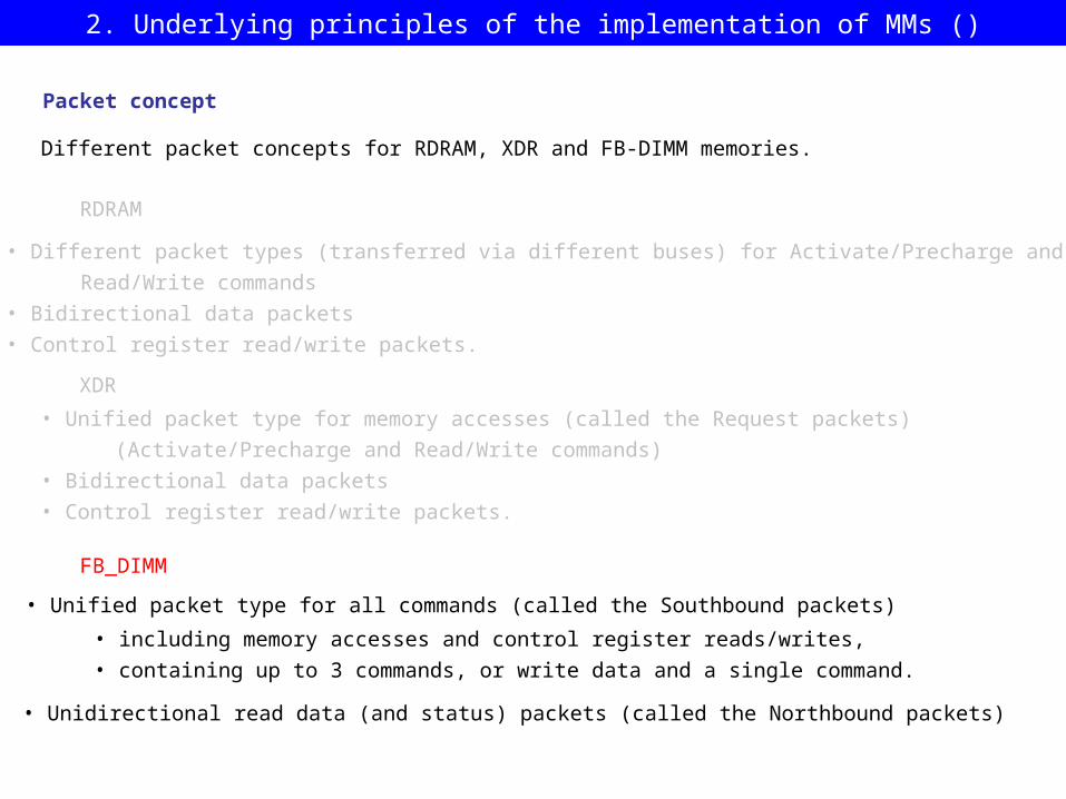
Packet concept
Different packet concepts for RDRAM, XDR and FB-DIMM memories.

Figure: RDRAM: Different packet types for Activate/Precharge and Read/Write commands [9]
2. Underlying principles of the implementation of MMs ()
Activate
Read
The packet concept of RDRAM memories (1)

• Data packets over the bidirectional data bus (DQA/DQB) • Row packets over the ROW bus • Column packets over the COL bus• CR R/W packets over the Serial bus
Figure: RDRAM: Memory access packets [10]
Row packets Column packets Datapackets
CR: Control RegisterR/W: Read/Write
2. Underlying principles of the implementation of MMs ()
The packet concept of RDRAM memories (2)

2. Underlying principles of the implementation of MMs ()
Packet concept
Different packet concepts for RDRAM, XDR and FB-DIMM memories.
RDRAM
• Different packet types (transferred via different buses) for Activate/Precharge and
Read/Write commands• Bidirectional data packets• Control register read/write packets.

Figure: The packet concept of XDR memories
[11]
Data packets
Requestpackets
CR R/Wpackets
2. Underlying principles of the implementation of MMs ()
The packet concept of XDR memories

2. Underlying principles of the implementation of MMs ()
Packet concept
Different packet concepts for RDRAM, XDR and FB-DIMM memories.
RDRAM
• Different packet types (transferred via different buses) for Activate/Precharge and
Read/Write commands• Bidirectional data packets• Control register read/write packets.
XDR
• Unified packet type for memory accesses (called the Request packets)
(Activate/Precharge and Read/Write commands)• Bidirectional data packets• Control register read/write packets.

Southbound packets
Memorycontroller
M. module
• Commands• Write data
M. module
M. module
Northbound packets• Read data• Status
Figure: The packet concept of FB-DIMM memories
2. Underlying principles of the implementation of MMs ()
The packet concept of FB-DIMM memories
2. Underlying principles of the implementation of MMs ()
Packet concept
Different packet concepts for RDRAM, XDR and FB-DIMM memories.
RDRAM
• Different packet types (transferred via different buses) for Activate/Precharge and
Read/Write commands• Bidirectional data packets• Control register read/write packets.
XDR
• Unified packet type for memory accesses (called the Request packets)
(Activate/Precharge and Read/Write commands)• Bidirectional data packets• Control register read/write packets.
FB_DIMM
• Unified packet type for all commands (called the Southbound packets)
• including memory accesses and control register reads/writes,• containing up to 3 commands, or write data and a single command.
• Unidirectional read data (and status) packets (called the Northbound packets)

2. Underlying principles of the implementation of MMs ()
Bus topology
Multi-drop bus Point-to-point connection
Stub-bus Fly-by Daisy-chained
Figure: Bus topologies used to connect DRAM devices or modules to the memory controller
Allows to connect more than onedevices/modules to the bus
Allows to interconnect two units(e.g. a mem. controller and a module)
Connection viaslots (sockets)
E.g.
MCDIMM
DIMM

Figure: Stub bus topology [3]
2. Underlying principles of the implementation of MMs ()

2. Underlying principles of the implementation of MMs ()
Bus topology
Multi-drop bus Point-to-point connection
Stub-bus Fly-by Daisy-chained
Figure: Bus topologies used to connect DRAM devices or modules to the memory controller
Allows to connect more than onedevices/modules to the bus
Allows to interconnect two units(e.g. a mem. controller and a module)
Connection viaslots (sockets)
Connection viasoldering
E.g.
MCDIMM
DIMM
MCDRAM
DRAM

Figure: Fly-by topology of the RQ bus in a two-channel XDR memory with two XDR devices/channel [5]
Fly-by topology
2. Underlying principles of the implementation of MMs ()

2. Underlying principles of the implementation of MMs ()
Bus topology
Multi-drop bus Point-to-point connection
Stub-bus Fly-by Daisy-chained
Figure: Bus topologies used to connect DRAM devices or modules to the memory controller
Allows to connect more than onedevices/modules to the bus
Allows to interconnect two units(e.g. a mem. controller and a module)
Connection viaslots (sockets)
Connection viasoldering
Connecting units to each other
(outputs to inputs)
E.g.
MCDIMM
DIMM
MCDRAM
DRAM
MCDIMM
DIMM

(There are two Command/Address buses (C/A) to reduce loading coming from 9 to 36 DRAMs mounted on the module)
Figure: Daisy chained topology of connecting AMBs in FB-DIMM memories [4]
2. Underlying principles of the implementation of MMs ()

2. Underlying principles of the implementation of MMs ()
Bus topology
Multi-drop bus Point-to-point connection
Stub-bus Fly-by Daisy-chained
Figure: Bus topologies used to connect DRAM devices or modules to the memory controller
Allows to connect more than onedevices/modules to the bus
Allows to interconnect two units(e.g. a mem. controller and a module)
Connection viaslots (sockets)
Connection viasoldering
Connecting units to each other
(outputs to inputs)
E.g.
MCDIMM
DIMM
MCDRAM
DRAM
MCDIMM
DIMM
MC
DRAM
DRAM

Figure: Point-to point topology of the data bus (DQ)in a two-channel XDR memory with two XDR devices/channel [5]
Point-to-point
2. Underlying principles of the implementation of MMs ()

2. Underlying principles of the implementation of MMs ()
Bus topology
Multi-drop bus Point-to-point bus
Stub-bus Fly-by bus Daisy-chained bus
Connecting DRAM
devices tothe MC
MCDRAM
DRAM
MC
DRAM
DRAM
Figure: Overview of bus topologies connecting DRAM devices to the memory controller
MCDRAM
DRAM
MCDRAM
DRAM
Used in Very early PCs RDRAMs(except theSerial bus)
XDR/XDR2(memory requests,
control registerreads/writes)
XDR/XDR2(read/write
data)

2. Underlying principles of the implementation of MMs ()
Figure: Overview of bus topologies connecting DRAM modules to the memory controller
MCDIMM
DIMM
Used in Parallel connectedmain memories
RIMMs(with fly-by device
connection on the module)MC
(FPM/EDO/SDRAM,DDR/DDR2/DDR3)
Bus topology
Multi-drop bus Point-to-point bus
Stub-bus Fly-by bus Daisy-chained bus
Connecting DIMMs tothe MC

2. Underlying principles of the implementation of MMs ()
Figure: Contrasting the interconnection of RIMM modules with that of DIMMs [12]

2. Underlying principles of the implementation of MMs ()
Connecting DIMMs tothe MC
MCDIMM
Figure: Overview of bus topologies connecting DRAM modules to the memory controller
MCDIMM
DIMM
MCDIMM
DIMM
Used in FB-DIMMs(to connect
AMBs)
Parallel connectedmain memories
MCDIMM
DIMM
RIMMs(with fly-by device
connection on the module)MC
(FPM/EDO/SDRAM,DDR/DDR2/DDR3)
Not feasible
Bus topology
Multi-drop bus Point-to-point bus
Stub-bus Fly-by bus Daisy-chained bus

2. Underlying principles of the implementation of MMs ()
Figure: Assessing bus topologies connecting DRAM devices/modules to the memory controller
Bus topology
Multi-drop bus Point-to-point bus
Stub-bus Fly-by bus Daisy-chained bus
Attaching DRAM
devices tothe MC
Attaching DIMMs tothe MC
Unfavorable(due to TL
discontinuities)Better Good Excellent Signal
integrity
Peak transfer rate
(recently)
Up to 16 Gb/s(with increasingly
sophisticated termination)
Up to 4.8 Gb/s
Up to 4.8 Gb/s
Up to 4.8 Gb/s
MCDRAM
DRAM
MC
DRAM
DRAM
MCDRAM
DRAM
MCDIMM
DIMM
MCDRAM
DRAM
MCDIMM
DIMM

Bus topologies of parallel connected synchronous MMs (Summary 1)
2. Underlying principles of the implementation of MMs ()
Synchronous DRAMs (except DDR3)
• read/write data
• commands • addresses
Stub bus
Stub bus
Stub bus
DDR3
• read/write data
• commands • addresses
Stub bus
Fly-by
Fly-by
DQ [3:0/7:0/15:0]
CS, RAS. CAS, WE
BA [7:0], A [N:0]
DQ [3:0/7:0/15:0]
CS, RAS. CAS, WE
BA [7:0], A [N:0]
I/O
I
I
I/O
I
I
Bus topologyBus designationBuses

Bus topologies of serial connected MMs (Summary 2)
XDR
• read/write data • memory requests) • control register (CR) reads
• control register (CR) writes
FB-DIMM (AMBs - memory controller)
• read data/device status • memory requests/ write data/CR reads or writes
Bus topology
Point-to-point
Fly-by
Fly-by
Fly-by
Daisy-chained
Daisy-chained
DQ [15:0]
RQ [11:0]
SDI
SDOPN [13:0]
PS [9:0]
2. Underlying principles of the implementation of MMs ()
Bus designation
• Read/write data
• Row bus
• Column bus
• Serial if.
CMD
, SIO1, SIO0
Fly-by
Fly-by
Fly-by
Fly-by
Fly-by
Daisy-chained
Buses
RDRAM
DQA [8:0], DQB [8:0]
ROW [2:0]
COL [4:0]
CMD
SIOI, SIOO
I/O
I
I
I/O
I/O
I/O
I
O
I
O
I

2. Underlying principles of the implementation of MMs ()
Figure: Bus topologies of current MMs to connect DRAM devices or modules to the memory controller
Address/control bus
Multi-drop bus Point-to-point
Stub-bus Fly-by bus Daisy-chained
Data
bu
s
Mu
lti-
dro
p b
us
P2
P
Stu
b-b
us
Fly
-by
Dais
y-c
hn
d
SDRAMDDR
DDR2(modules)
Devices onthe modules
DDR3
RDRAM(devices,modules)
XDR XDR2
(devices)
FB-DIMM(AMBs on modules)
TBI(devices)

2. Underlying principles of the implementation of MMs ()
Figure: Signal types used in MMs for control, address and data signals
Signals
Voltage referencedSingle ended Differential
LVDS: Low Voltage Differential Signaling LVTTL: Low Voltage TTL(D)RSL: (Differential) Rambus Signaling Level SSTL: Stub Series Terminated Logic VCM: Common Mode Voltage VREF: Reference Voltage
t t
VREF
LVTTL (3.3 V) FPM/EDO SDRAM
TTL (5 V)
FPM/EDO
SSTL SSTL2 (DDR) SSTL1.8 (DDR2) SSTL1.5 (DDR3)RSL (RDRAM)
LVDS FB-DIMMs
t
S+
S-VCM
Smaller voltage swings
Typ.voltageswings 600-800 mV
DRSL XDR (data)
200-300 mV3.3-5 V
Used in

shorter signal rise/fall times higher speed grades
but lower voltage budget higher requirements for signal integrity
2. Underlying principles of the implementation of MMs ()
Smallervoltageswings
Q = Cin x V = I x t tR ~ Cin x V/I
Q: Charge on the input capacitance of the line (Cin)Cin: Input capacitance of the line V: Voltage I: Current strength of the driver tR: Rise time
Voltage swing vs signal rise/fall time

Bus topologies and signaling of parallel connected MMs (Summary 1)
2. Underlying principles of the implementation of MMs ()
Synchronous DRAMs (except DDR3)
• read/write data
• commands • addresses
Stub bus
Stub bus
Stub bus
DDR3
• read/write data
• commands • addresses
Stub bus
Fly-by
Fly-by
DQ [3:0/7:0/15:0]
CS, RAS. CAS, WE
BA [7:0], A [N:0]
DQ [3:0/7:0/15:0]
CS, RAS. CAS, WE
BA [7:0], A [N:0]
I/O
I
I
I/O
I
I
Bus topologyBus designationBuses Signaling
Volt. ref.
Volt. ref.
Volt. ref.
Volt. ref.
Volt. ref.
Volt. ref.

Bus topologies and signaling of serial connected MMs (Summary 2)
XDR
• read/write data • memory requests) • control register (CR) reads
• control register (CR) writes
FB-DIMM (AMBs - memory controller)
• read data/device status • memory requests/ write data/CR reads or writes
Bus topology
Point-to-point
Fly-by
Fly-by
Fly-by
Daisy-chained
Daisy-chained
DQ [15:0]
RQ [11:0]
SDI
SDOPN [13:0]
PS [9:0]
2. Underlying principles of the implementation of MMs ()
Bus designation
• Read/write data
• Row bus
• Column bus
• Serial if.
CMD
, SIO1, SIO0
Fly-by
Fly-by
Fly-by
Fly-by
Fly-by
Daisy-chained
Buses
RDRAM
DQA [8:0], DQB [8:0]
ROW [2:0]
COL [4:0]
CMD
SIOI, SIOO
I/O
I
I
I/O
I/O
I/O
I
O
I
O
I
Differential
Volt. ref.
Volt. ref.
Volt. ref.
Differential
Differential
Signaling
Volt ref.
Volt. ref.
Volt. ref.
CMOS
Volt. ref.
Volt. ref.

2. Underlying principles of the implementation of MMs ()
Capturing control/address information
Centralsynchronization
Sourcesynchronization
Mesochronoussynchronization
The sourcing device (MC or DRAM)sends a strobe signal
along with the signals sent
A central clock signal is usedto latch the signals
Keeps the clock frequency betweenthe sender reference clock and the
receiver reference clock but not the phase relationship.
Synchronisation

Figure: Central clocking of address, command and data lines in an SDRAM devicewhile writing random data [6]
Address, command and data lines arelatched by the rising edge of the central clock (CLK)
Central clocking (SDRAM)
2. Underlying principles of the implementation of MMs ()

Figure: Source synchronous clocking (DDR SDRAMs) of the data lines in a DDR device while writing random data [7]
(TDOSS: Write command to first DQS latching transition)
Command and address lines are latched by the differential clock (CK, CK#) butwrite data are latched by the rising edge of the source synchronous data strobe (DQS)
Source synchronous clocking of the data lines (DDR)
2. Underlying principles of the implementation of MMs ()

Mesochronous clocking (FB-DIMM)
Figure: Mesochronous clocking used to synchronise AMBs in FB-DIMM memories [8]
2. Underlying principles of the implementation of MMs ()

2. Underlying principles of the implementation of MMs ()
Figure: Synchronisation alternatives
SDRAM
RDRAMXDR3
XDR23
Capturing control/address information
Centralsynchronization
Sourcesynchronization
Mesochronoussynchronization
Cap
turi
ng
data
Sou
rce
syn
ch
.
Mesoch
ron
.syn
ch
.
FBDIMM
Cen
tral
syn
ch
.
DDR1
DDR22
DDR32
1: Phase alignement for data reads/writes2: Phase alignement for data reads/writes by read/write leveling3: Phase alignement for all signals by FlexPhase
DDRX?

3. Performance considerations (1)
Figure: Peak memory size vs peak bandwidth (BW) of particular DRAM technologies in Intel’s desktop chipsets
1
100
2
2
20
5
0,5
10 20
10
1
30
200
50
5
500
BW GB/s
Mem. SizeGB
DDR2
P35 (2)x
925X (2)x
X48x
P45 (2)x
845 (1)
850E (1)
820 (1)850 (1) x
875 (2)
x
DDR
x
845 (1)
DDR3
Core 2 Desktop
RDRAM
P4 Desktops
P4 Desktops
192
512
32
48
x
x
P4 Desktops
SDRAM
16
8
4
3
0,75
1,06 1,6 3,2 4,2 6,4 8,5 10,6 12,8 21,2 25,6
50
51,2
P45 (2)x
17,7

1
100
2
2
20
5
0,5
10 20
10
1
30
200
50
5
500
BW GB/s
Mem. SizeGB
QS21 (2D)x
P4 Servers, QS22
5100 (2)x
P4 Servers
x
x7520 (2)
7501 (2)
QS22 (2) (2D)
x
7520 (2)x
x840 (2)
x7300 (4)
FB-DIMMDDR-2
Core 2 Servers, T2
DDR2 (reg)
DDR(reg)
RDRAM
P4 Servers
XDR Servers
192
512
32
48
x860 (2)
xQS20 (2D)
16
8
4
3
0,75
1,06 1,6 3,2 4,2 6,4 8,5 10,6 12,8 21,2 25,6
Figure: Peak memory size vs peak bandwidth (BW) of particular DRAM technologies in Intel’s server chipsets, IBM’s QS2x blades and Sun’s T2
xSunT2 (4D)
50
51,2
3. Performance considerations (2)

4. References
References
[1]: Yeung P., „Solving System Engineering Challenges in High Speed Memory Designs,” Rambus Design Seminar, Feb. 21 2008, http://www.rambus.com/us/events/papers_and_presentations/index.html
[2]: http://www.pricegrabber.com/search_getprod.php/masterid=3191326
[3]: Reddy A., „XDR and XDR2 Overview,”, RDF, Oct. 18 2007, Taiwan, http://www.rambus.com/us/events/papers_and_presentations/index.html
[4]: McTague M. & David H., „ Fully Buffered DIMM (FB-DIMM) Design Considerations,” Febr. 18, 2004, Intel Developer Forum, http://www.idt.com/content/OSA-S009.pdf
[5]: Yoshitomi Y., „Elpida DRAM Solutions to Advanced Digital Consumer Electronic Systems,” Rambus Design Seminar, Hsinchu, Elpida, June 26 2008, http://www.rambus.com/us/events/papers_and_presentations/index.html
[6]: Micron Synchronous DRAM, 64 Mbit, MT48LC16M4A2, MT48LC16M8A2, MT48LC16M16A2, Micron Technology, Inc. http://www.micron.com/products/dram/sdram/partlist.aspx Oct. 2000
[7]: Double Data Rate (DDR) SDRAM MT46V128M4, MT46V64M8, MT46V32M16, Micron Techn. Inc, 2000, http://download.micron.com/pdf/datasheets/dram/ddr/512MBDDRx4x8x16.pdf
[8]: FBDIMM Specification: High Speed Differential Point-to-Point Link at 1.5 V, JESD8-18, Sept. 2006, JEDEC

4. References
[9]: Direct Rambus Architecture and Measurements, MindShare, http://www.mindshare.com
[10]: Crisp R., Direct Rambus Technology: The New Main Memory Standard,”, IEEE Micro, Nov./Dez. 1997, pp. 18-28
[11]: Ishikawa T., „Elpida XDRAM,”, RDF Oct. 18 2007, Taiwan http://www.rambus.com/us/events/papers_and_presentations/index.html
[12]: DeMone P., „Direct Rambus Memory,” Real Word Technologies, 11-7-1999, http://www.realworldtech.com/page.cfm?ArticleID=RWT110799000000&p=1


