DEVICENET CAN TRANSCEIVERS - TI. · PDF fileSN65HVD252 SN65HVD253 SLLSE37 – JUNE 2010...
18
SN65HVD252 CANH CANL V REF S 8 7 6 5 GND V CC RXD TXD 1 2 3 4 V CC /2 SN65HVD253 V CC CANH CANL AB S 8 7 6 5 GND RXD TXD 1 2 3 4 SN65HVD252 SN65HVD253 www.ti.com SLLSE37 – JUNE 2010 DeviceNet™ CAN Transceivers Check for Samples: SN65HVD252, SN65HVD253 1FEATURES APPLICATIONS • DeviceNet Networks (Vendor ID # 806) 2• DeviceNet Compliant Supporting 64 DeviceNet Nodes • Industrial Automation • HVAC Networks • Loopback Function (HVD253) • Security Systems • Bus-Fault Protection of –36 V to 40 V • Telecom Base Station Status and Control • Power-Up/Down Glitch-Free Bus I/O • CANopen Data Bus • 3.3-V Compatible Receiver Output • SDS Data Bus • CAN Kingdom Data Bus DESCRIPTION The SN65HVD252 and SN65HVD253 CAN transceivers meet or exceed the specifications of DeviceNet and are compatible to the ISO 11898-2:2003 standard for use in applications employing a controller area network (CAN). This device provides differential transmit and receive capability at signaling rates up to 1 megabit per second (Mbps). Designed for operation in harsh industrial environments, these devices feature bus-pin voltage protection from –36 V to 40 V, driver output current limiting, and overtemperature driver shutdown. Pin 8 provides for two different modes of operation: normal and silent mode. The normal mode of operation is selected by connecting S (pin 8) to ground. If a high logic level is applied to the S pin, the device enters a listen-only silent mode during which the driver is inactive while the receiver remains fully functional. The Vref pin 5 of the SN65HVD252 is a V CC /2 voltage reference for systems which use split termination. The AB pin of the SN65HVD253 implements a listen-only loopback feature which allows the local node controller to synchronize its baud rate with that of the CAN bus. In loopback mode, the driver differential outputs are placed in high-impedance state while the receiver bus inputs remain active. For more information on the loopback mode, see the Application Information section. The SN65HVD252 and SN65HVD253 are characterized for operation from –40°C to 85°C. SPACER 1 Please be aware that an important notice concerning availability, standard warranty, and use in critical applications of Texas Instruments semiconductor products and disclaimers thereto appears at the end of this data sheet. 2DeviceNet is a trademark of Open DeviceNet Vendor Association . PRODUCTION DATA information is current as of publication date. Copyright © 2010, Texas Instruments Incorporated Products conform to specifications per the terms of the Texas Instruments standard warranty. Production processing does not necessarily include testing of all parameters.
Transcript of DEVICENET CAN TRANSCEIVERS - TI. · PDF fileSN65HVD252 SN65HVD253 SLLSE37 – JUNE 2010...

SN65HVD252
CANH
CANL
VREF
S8
7
6
5
GND
VCC
RXD
TXD1
2
3
4V
CC/ 2
SN65HVD253
VCC
CANH
CANL
AB
S8
7
6
5
GND
RXD
TXD1
2
3
4
SN65HVD252SN65HVD253
www.ti.com SLLSE37 –JUNE 2010
DeviceNet™ CAN TransceiversCheck for Samples: SN65HVD252, SN65HVD253
1FEATURES APPLICATIONS• DeviceNet Networks (Vendor ID # 806)
2• DeviceNet Compliant Supporting 64 DeviceNetNodes • Industrial Automation
• HVAC Networks• Loopback Function (HVD253)• Security Systems• Bus-Fault Protection of –36 V to 40 V• Telecom Base Station Status and Control• Power-Up/Down Glitch-Free Bus I/O• CANopen Data Bus• 3.3-V Compatible Receiver Output• SDS Data Bus• CAN Kingdom Data Bus
DESCRIPTIONThe SN65HVD252 and SN65HVD253 CAN transceivers meet or exceed the specifications of DeviceNet and arecompatible to the ISO 11898-2:2003 standard for use in applications employing a controller area network (CAN).This device provides differential transmit and receive capability at signaling rates up to 1 megabit per second(Mbps).
Designed for operation in harsh industrial environments, these devices feature bus-pin voltage protection from–36 V to 40 V, driver output current limiting, and overtemperature driver shutdown.
Pin 8 provides for two different modes of operation: normal and silent mode. The normal mode of operation isselected by connecting S (pin 8) to ground. If a high logic level is applied to the S pin, the device enters alisten-only silent mode during which the driver is inactive while the receiver remains fully functional.
The Vref pin 5 of the SN65HVD252 is a VCC/2 voltage reference for systems which use split termination.
The AB pin of the SN65HVD253 implements a listen-only loopback feature which allows the local node controllerto synchronize its baud rate with that of the CAN bus. In loopback mode, the driver differential outputs are placedin high-impedance state while the receiver bus inputs remain active. For more information on the loopback mode,see the Application Information section.
The SN65HVD252 and SN65HVD253 are characterized for operation from –40°C to 85°C.
SPACER
1
Please be aware that an important notice concerning availability, standard warranty, and use in critical applications of TexasInstruments semiconductor products and disclaimers thereto appears at the end of this data sheet.
2DeviceNet is a trademark of Open DeviceNet Vendor Association .
PRODUCTION DATA information is current as of publication date. Copyright © 2010, Texas Instruments IncorporatedProducts conform to specifications per the terms of the TexasInstruments standard warranty. Production processing does notnecessarily include testing of all parameters.

TXD 1
2
3
4
8
7
6
5
GND
VCC
RXD
S
CANH
CANL
AB
HVD253
TXD 1
2
3
4
8
7
6
5
GND
VCC
RXD
S
CANH
CANL
VREF
HVD252
SN65HVD252SN65HVD253SLLSE37 –JUNE 2010 www.ti.com
These devices have limited built-in ESD protection. The leads should be shorted together or the device placed in conductive foamduring storage or handling to prevent electrostatic damage to the MOS gates.
Table 1. DRIVER (SN65HVD252)
INPUTS OUTPUTSBUS STATE
TXD S CAN_H CAN_L
L H L DominantL or OPEN
H or OPEN Z Z Recessive
X H Z Z Recessive
Table 2. RECEIVER (SN65HVD252)
INPUTS OUTPUT
BUS STATE VID = VCANH – VCANL RXD
Dominant VID ≥ 0.9 V L
? 0.5 V < VID < 0.9 V ?
Recessive VID < 0.5 V H
OPEN VID ≈ 0 V H
Table 3. DRIVER (SN65HVD253)
INPUTS OUTPUTSBUS STATE
TXD AB S CAN_H CAN_L
X X H Z Z Recessive
L L or open H L Dominant
H or open X L or OPEN Z Z Recessive
X H Z Z Recessive
Table 4. RECEIVER (SN65HVD253)
INPUTS OUTPUT
AB BUS STATE VID = VCANH – VCANL TXD RXD
Dominant VID ≥ 0.9 V L
? 0.5 V < VID < 0.9 V ?L or open X
Recessive VID ≤ 0.5 V H
Open VID ≈ 0 V H
Dominant VID ≥ 0.9 V X L
L LH ? 0.5 V < VID < 0.9 V
H ?
Recessive VID ≤ 0.5 V or open H H
X X X L L
2 Submit Documentation Feedback Copyright © 2010, Texas Instruments Incorporated
Product Folder Link(s): SN65HVD252 SN65HVD253

SN65HVD252SN65HVD253
www.ti.com SLLSE37 –JUNE 2010
ABSOLUTE MAXIMUM RATINGS (1)
VALUE UNIT
Supply voltage (2), VCC –0.3 to 6 V
Voltage range at CANH, CANL, VREF –36 to 40 V
Voltage at CANH, CANL, transient pulse per ISO 7637, pulse 1, 2, 3a, 3b, 5, 6, 7 –200 to 200 V
Voltage input range at logic inputs, VI (TXD, AB, RXD, S) –0.5 to 6 V
ESD, human-body model (HBM) per JEDEC Standard 22, test method A114, CANH, CANL vs GND ±12 kV
ESD, human-body model (HBM) per JEDEC Standard 22, test method A114, all pins ±5 kV
ESD, charged-device model (CDM) per JEDEC Standard 22, test method C101, all pins ±2 kV
ESD, machine model (MM) per JEDEC Standard 22, test method A115 CANH, CANL vs GND ±200 V
Receiver output current, IO ±20 mA
Junction temperature, TJ 170 °C
(1) Stresses beyond those listed under Absolute Maximum Ratings may cause permanent damage to the device. These are stress ratingsonly, and functional operation of the device at these or any other conditions beyond those indicated under Recommended OperatingConditions is not implied. Exposure to absolute-maximum-rated conditions for extended periods may affect device reliability.
(2) All voltage values, except differential I/O bus voltages, are with respect to ground terminal.
RECOMMENDED OPERATING CONDITIONSMIN MAX UNIT
VCC Supply voltage 4.75 5.25 V
Voltage at any bus terminal (separately or common mode) –5 (1) 10 V
VIH High-level input voltage 2 5.5 VTXD, S, AB inputs
VIL Low-level input voltage 0 0.8 V
VID Differential input voltage –7 7 V
Driver –70 70IOH Output current mA
Receiver –2 2
Operating ambient free-airTA See Thermal Information Table –40 85 °Ctemperature
(1) The algebraic convention, in which the least positive (most negative) limit is designated as minimum is used in this data sheet.
Copyright © 2010, Texas Instruments Incorporated Submit Documentation Feedback 3
Product Folder Link(s): SN65HVD252 SN65HVD253

SN65HVD252SN65HVD253SLLSE37 –JUNE 2010 www.ti.com
THERMAL INFORMATIONHVD252/53
THERMAL METRIC UNITS8 PINS SOIC
qJA Junction-to-ambient thermal resistance (1) 124.5
qJC(top) Junction-to-case(top) thermal resistance (2) 55.9
qJB Junction-to-board thermal resistance (3) 50.2°C/W
yJT Junction-to-top characterization parameter (4) 4.9
yJB Junction-to-board characterization parameter (5) 46
qJC(bottom) Junction-to-case(bottom) thermal resistance (6) n/a
VCC = 5 V, TJ = 27°C, RL = 60Ω,RS at 0 V, Input to D a 500-kHz 189.1 mW50% duty cycle square wave
PD Device power dissipationVCC = 5.25 V, TJ = 150°C, RL = 50Ω,RS at 0 V, Input to D a 500-kHz 274.8 mW50% duty cycle square wave
(1) The junction-to-ambient thermal resistance under natural convection is obtained in a simulation on a JEDEC-standard, high-K board, asspecified in JESD51-7, in an environment described in JESD51-2a.
(2) The junction-to-case (top) thermal resistance is obtained by simulating a cold plate test on the package top. No specificJEDEC-standard test exists, but a close description can be found in the ANSI SEMI standard G30-88.
(3) The junction-to-board thermal resistance is obtained by simulating in an environment with a ring cold plate fixture to control the PCBtemperature, as described in JESD51-8.
(4) The junction-to-top characterization parameter, yJT, estimates the junction temperature of a device in a real system and is extractedfrom the simulation data for obtaining qJA, using a procedure described in JESD51-2a (sections 6 and 7).
(5) The junction-to-board characterization parameter, yJB, estimates the junction temperature of a device in a real system and is extractedfrom the simulation data for obtaining qJA , using a procedure described in JESD51-2a (sections 6 and 7).
(6) The junction-to-case (bottom) thermal resistance is obtained by simulating a cold plate test on the exposed (power) pad. No specificJEDEC standard test exists, but a close description can be found in the ANSI SEMI standard G30-88.
DRIVER ELECTRICAL CHARACTERISTICSover recommended operating conditions (unless otherwise noted)
PARAMETER TEST CONDITIONS MIN TYP (1) MAX UNIT
CANH 2.75 3.5 4.5Bus output voltage See Figure 1, TXD = 0 V, S = 0 V, AB = 0 V (HVD253),VO(D) V(dominant) RCM = open, CL = open, RL = 60 ΩCANL 0.5 1.5 2.25
VO(R) Bus output voltage (recessive) TXD = 3 V, S = 0 V No Load 2 2.5 3 V
See Figure 1, TXD = 0 V, S = 0 V, RCM = open,1.5 2.4 3.4
CL = open, 45 Ω ≤ RL ≤ 60 ΩDifferential output voltageVOD(D) V(dominant) See Figure 1, TXD = 0 V, S = 0 V, RL = 60 Ω, 1.2 2.6 3.3RCM = 330 Ω, CL = open, –5 V < VCM < 10 V
RL = 60 Ω –12 12Differential output voltage See Figure 1, TXD = 3 V, S = 0 V,VOD(R) mV(recessive) RCM = open, CL = 100 pF No load –100 50
Output symmetry (dominant or See Figure 1, S = 0 V, AB = 0 V (HVD253), RCM = open,VSYM –400 0 400 mVrecessive) CL = open, RL = 60 Ω, VSYM = VCC – VCANH – VCANL
–5 V < VCANH < 10 V, CANL open –350 2.5Short-circuit steady-state outputIOS(ss) mAcurrent –5 V < VCANL < 10 V, CANH open –2.5 350
(1) All typical values are at 25°C with VCC = 5 V.
DRIVER SWITCHING CHARACTERISTICSPARAMETER TEST CONDITIONS MIN TYP MAX UNIT
tpHR Propagation delay time, high input to recessive output 50 70
tpLD Propagation delay time, low input to dominant output 40 70See Figure 1, S = 0 V, RL = 60 Ω, nsCL = 100 pF, RCM = opentr Differential output signal rise time, 10% to 90% 15 30
tf Differential output signal fall time, 90% to 10% 17 30
RL = 60 Ω, CL = 15 pF,ten Enable time from silent mode to dominant 200 nsCLD = 100 pF
4 Submit Documentation Feedback Copyright © 2010, Texas Instruments Incorporated
Product Folder Link(s): SN65HVD252 SN65HVD253

SN65HVD252SN65HVD253
www.ti.com SLLSE37 –JUNE 2010
RECEIVER ELECTRICAL CHARACTERISTICSover recommended operating conditions (unless otherwise noted)
PARAMETER TEST CONDITIONS MIN TYP (1) MAX UNIT
VIT+ Positive-going input threshold voltage 800 900
VIT– Negative-going input threshold voltage –5 V < VCM < 10 V 500 650 mV
Vhys Hysteresis voltage (VIT+ – VIT–) 140 160
IO = –2 mA 2.4 3.3 3.7VOH High-level output voltage V
IO = –20 µA 2.7 3.3 3.7
VOL Low-level output voltage IO = 2 mA 0.1 0.2 V
IBL(off) Bus leakage current, with power off Vcc at 0 V –600 600CANH or CANL,
µATXD or S pin atOther bus pin at 0 VIBL Bus leakage current, in silent mode or recessive state –600 600VCC
CI Input capacitance to ground, (CANH or CANL) VI = 0.4 sin (4E6pt) + 2.5 V 20 pF
CID Differential input capacitance VI = 0.4 sin (4E6pt) 7 pF
RID Differential input resistance TXD at 3 V, S at 0 V 30 60 80 kΩRIN Input resistance, (CANH or CANL) 15 30 40 kΩ
Input resistance matchingRI(M) VCANH = VCANL –3% 0% 3%
[1 – (RIN (CANH) / RIN (CANL))] × 100%
(1) All typical values are at 25°C with VCC = 5 V.
RECEIVER SWITCHING CHARACTERISTICSover recommended operating conditions (unless otherwise noted)
PARAMETER TEST CONDITIONS MIN TYP MAX UNIT
tpRH Propagation delay time, recessive input to high output 55 80
tpDL Propagation delay time, dominant input to low output 50 80See Figure 2, CL = 15 pF,ns
AB = 0 V or VCC (HVD253)tr Output signal rise time, 10% to 90% 20
tf Output signal fall time, 90% to 10% 20
DRIVER-TO-RECEIVER LOOP-SWITCHING CHARACTERISTICSover recommended operating conditions (unless otherwise noted)
PARAMETER TEST CONDITIONS MIN TYP MAX UNIT
Recessive totloop1 40 90 140See Figure 4, S at 0 V, AB at 0 V,Total loop delay, driver input dominant nsto receiver output RL = 60 Ω, CLD = 100 pF, CL = 15 pFtloop2 Dominant to recessive 40 105 140
See Figure 5, S at 0 V, AB = VCC,Loopback delay, driver input to receiver outputtAB1 20 40 ns(HVD253 only) RL = 60 Ω, CLD = 100 pF, CL = 15 pF
Copyright © 2010, Texas Instruments Incorporated Submit Documentation Feedback 5
Product Folder Link(s): SN65HVD252 SN65HVD253

SN65HVD252SN65HVD253SLLSE37 –JUNE 2010 www.ti.com
LOGIC INPUT PIN CHARACTERISTICS (D, S, AND AB INPUTS)over recommended operating conditions (unless otherwise noted)
PARAMETER TEST CONDITIONS MIN TYP MAX UNIT
II Input current 0 V < VIN < VCC –100 100 µA
IOP(off) Power-off leakage current VCC at 0 V, 0 < VIN < VCC(MAX) –100 100 µA
VREF PIN CHARACTERISTICSover recommended operating conditions (unless otherwise noted)
PARAMETER TEST CONDITIONS MIN TYP MAX UNIT
–100 µA < IO < 100 µA 0.4 VCC 0.5VCC 0.6VCC
VO Output voltage –50 µA < IO < 50 µA 0.43 VCC 0.5VCC 0.57 VCC V
–5 µA < IO < 5 µA 0.45 VCC 0.5VCC 0.55 VCC
SUPPLY CURRENTover recommended operating conditions (unless otherwise noted)
PARAMETER TEST CONDITIONS MIN TYP MAX UNIT
HVD252 S at VCC, TXD at VCC 13 17Silent
HVD253 S at VCC, AB at 0 V or VCC 13 17ICC Supply current mA
Dominant TXD at 0 V, 50-Ω load, S at 0 V 60 80All
Recessive TXD at VCC, no load, S at 0 V 13 17
6 Submit Documentation Feedback Copyright © 2010, Texas Instruments Incorporated
Product Folder Link(s): SN65HVD252 SN65HVD253
VODRL
CANH
CANL
TXD
RCM
RCM
VCMCL
10%
90%0.9V
0 V
0.5V
tpLD tpHR
3 V
tftr
TXD
VOD
50% 50%
VOCL
CANH
RXD
CANL
VID
VID0 .5V
0 .9V1 .5 V
0 V
VO(RXD)
VOH
VOL
50%
tpRH
tpDL
tftr
90%
10%
SN65HVD252SN65HVD253
www.ti.com SLLSE37 –JUNE 2010
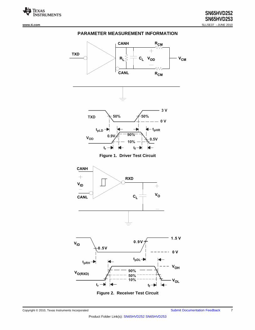
PARAMETER MEASUREMENT INFORMATION
Figure 1. Driver Test Circuit
Figure 2. Receiver Test Circuit
Copyright © 2010, Texas Instruments Incorporated Submit Documentation Feedback 7
Product Folder Link(s): SN65HVD252 SN65HVD253

RL
CANH
CANL
TXDC
L
VO C
L
RXD
SV
I
0V
ten
S
RXD
VOH
VOL
3 V
50%
50%
0 V
RL
CANH
CANL
TXDCLD
VO CL
RXD
S
VI
0V
tloop1
TXD
RXD
VOH
VOL
3 V
tloop2
50%
50%
0 V
SN65HVD252SN65HVD253SLLSE37 –JUNE 2010 www.ti.com
PARAMETER MEASUREMENT INFORMATION (continued)
Figure 3. Enable Test Circuit
Figure 4. Loop Time Measurements
8 Submit Documentation Feedback Copyright © 2010, Texas Instruments Incorporated
Product Folder Link(s): SN65HVD252 SN65HVD253

RL
CANH
CANL
TXDCLD
VO CL
RXD
AB
VI
VCC
TXD
RXD
VOH
VOL
3 V
50%
50%
tAB(HL)tAB(LH)
0 V
SN65HVD252SN65HVD253
www.ti.com SLLSE37 –JUNE 2010
PARAMETER MEASUREMENT INFORMATION (continued)
Figure 5. Loopback Timing Measurement
Copyright © 2010, Texas Instruments Incorporated Submit Documentation Feedback 9
Product Folder Link(s): SN65HVD252 SN65HVD253
3.3 VRXD Output
6 V
Output15 ?
VCC
V OutputREF
Output
3 k?
3 k?
40 V
S and AB Inputs
VCC
4.3 k
6 V
Input
?
VCC
40 V
CANL
CANH and CANL Outputs
CANH Input
VCC
20 k
40 V
Input
10 k?
10 k?
?
TXD Input
VCC
4.3 k
6 V
Input?
CANL Input
VCC
20 k
40
V
Input
10 k?
10 k?
?
40 V
CANH
140 k?
SN65HVD252SN65HVD253SLLSE37 –JUNE 2010 www.ti.com
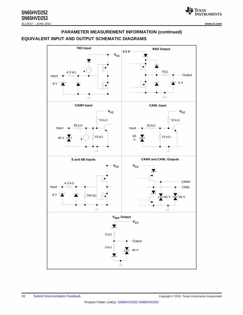
PARAMETER MEASUREMENT INFORMATION (continued)
EQUIVALENT INPUT AND OUTPUT SCHEMATIC DIAGRAMS
10 Submit Documentation Feedback Copyright © 2010, Texas Instruments Incorporated
Product Folder Link(s): SN65HVD252 SN65HVD253

SN65HVD252SN65HVD253
www.ti.com SLLSE37 –JUNE 2010
APPLICATION INFORMATION
USING THE SILENT MODE
The silent mode is selected by setting a logic high on pin 8 (S). In silent mode, the driver function of thetransceiver is disabled, whereas the receiver function remains active. This silent mode may be used toimplement babbling idiot protection, to ensure that the driver does not disrupt the entire network in case of a localfault. The silent mode may also be used in redundant systems to select or de-select the redundant transceiveruntil needed.
USING THE AUTOBAUD FEATURE OF THE SN65HVD253
The autobaud feature of the HVD253 is selected by placing a logic high on pin 5 (AB). In autobaud mode, thenormal bus-transmit function of the transceiver is disabled, whereas the bus-receive function and all of the othernormal operating functions of the device remain active. An internal loopback emulates the connection betweenthe driver outputs and the receiver inputs, allowing the receiver to respond to locally-generated dominant bits aswell as dominant bits from other nodes.
With the autobaud function engaged, normal bus activity, including activity from the local controller, can bemonitored by the local node as received data. However, if an error frame is generated by the local CANcontroller, it is not transmitted to the bus. Only the local microprocessor can detect the error frame.
Autobaud detection is well suited to applications that have a known selection of baud rates. For example,DeviceNet (a common industrial protocol) has optional signaling rates of 125 kbps, 250 kbps, or 500 kbps. Oncea logic high has been applied to pin 5 (AB) of the HVD253, the local controller may assume a baud rate such as125 kbps and then wait for a message to be transmitted by another node on the bus. If the wrong local signalingrate has been selected, an error message is generated by the local CAN controller. However, because thebus-transmit function of the transceiver has been disabled, no other nodes receive the error message from thelocal controller.
This procedure makes use of the CAN controller status-register indications of message received and errorwarning status to signal if the current signaling rate is correct or not. The warning status indicates that the CANcontroller error counters have been incremented. A message-received status indicates that a good message hasbeen received.
If an error is generated, the local CAN controller may assume another signaling rate and wait to receive anothermessage. When an error-free message has been received, the correct baud rate has been selected. A logic lowmay now be applied to pin 5 (AB) of the HVD253, returning the bus-transmit normal operating function to thetransceiver.
USING THE VREF OUTPUT
The VREF output provides a stable voltage of half the power supply voltage. This can be used in split-terminationschemes to improve electromagnetic compatibility (EMC) of the system. It can also be used as a reference withwhich to compare the single-ended inputs for degraded operation in the event of a wire-break fault on either theCANH or CANL bus lines.
DeviceNet REQUIREMENTS
DeviceNet requires additional performance beyond the requirements of the ISO 11898-2 CAN standard. Theseadditional specifications address the conditions found in rugged industrial applications. The DeviceNetspecifications are maintained by ODVA. (www.odva.org) The HVD252 and HVD253 fully meet theserequirements under all recommended operating conditions.
PARAMETER DeviceNet SPECIFICATION HVD252, HVD253
Number of nodes 64 Yes
Minimum differential input resistance 20 kΩ Yes
Minimum differential input capacitance 24 pF Yes
Bus pin voltage range (survivable) –25 V to 18 V Yes
Bus pin voltage range (operation) –5 V to 10 V Yes
Differential output voltage 1.5 V with 50-Ω load Yes
Copyright © 2010, Texas Instruments Incorporated Submit Documentation Feedback 11
Product Folder Link(s): SN65HVD252 SN65HVD253

PACKAGE OPTION ADDENDUM
www.ti.com 11-Apr-2013
Addendum-Page 1
PACKAGING INFORMATION
Orderable Device Status(1)
Package Type PackageDrawing
Pins PackageQty
Eco Plan(2)
Lead/Ball Finish MSL Peak Temp(3)
Op Temp (°C) Top-Side Markings(4)
Samples
SN65HVD252D ACTIVE SOIC D 8 75 Green (RoHS& no Sb/Br)
CU NIPDAU Level-1-260C-UNLIM -40 to 85 HVD252
SN65HVD252DR ACTIVE SOIC D 8 2500 Green (RoHS& no Sb/Br)
CU NIPDAU Level-1-260C-UNLIM -40 to 85 HVD252
SN65HVD253D ACTIVE SOIC D 8 75 Green (RoHS& no Sb/Br)
CU NIPDAU Level-1-260C-UNLIM -40 to 85 HVD253
SN65HVD253DR ACTIVE SOIC D 8 2500 Green (RoHS& no Sb/Br)
CU NIPDAU Level-1-260C-UNLIM -40 to 85 HVD253
(1) The marketing status values are defined as follows:ACTIVE: Product device recommended for new designs.LIFEBUY: TI has announced that the device will be discontinued, and a lifetime-buy period is in effect.NRND: Not recommended for new designs. Device is in production to support existing customers, but TI does not recommend using this part in a new design.PREVIEW: Device has been announced but is not in production. Samples may or may not be available.OBSOLETE: TI has discontinued the production of the device.
(2) Eco Plan - The planned eco-friendly classification: Pb-Free (RoHS), Pb-Free (RoHS Exempt), or Green (RoHS & no Sb/Br) - please check http://www.ti.com/productcontent for the latest availabilityinformation and additional product content details.TBD: The Pb-Free/Green conversion plan has not been defined.Pb-Free (RoHS): TI's terms "Lead-Free" or "Pb-Free" mean semiconductor products that are compatible with the current RoHS requirements for all 6 substances, including the requirement thatlead not exceed 0.1% by weight in homogeneous materials. Where designed to be soldered at high temperatures, TI Pb-Free products are suitable for use in specified lead-free processes.Pb-Free (RoHS Exempt): This component has a RoHS exemption for either 1) lead-based flip-chip solder bumps used between the die and package, or 2) lead-based die adhesive used betweenthe die and leadframe. The component is otherwise considered Pb-Free (RoHS compatible) as defined above.Green (RoHS & no Sb/Br): TI defines "Green" to mean Pb-Free (RoHS compatible), and free of Bromine (Br) and Antimony (Sb) based flame retardants (Br or Sb do not exceed 0.1% by weightin homogeneous material)
(3) MSL, Peak Temp. -- The Moisture Sensitivity Level rating according to the JEDEC industry standard classifications, and peak solder temperature.
(4) Multiple Top-Side Markings will be inside parentheses. Only one Top-Side Marking contained in parentheses and separated by a "~" will appear on a device. If a line is indented then it is acontinuation of the previous line and the two combined represent the entire Top-Side Marking for that device.
Important Information and Disclaimer:The information provided on this page represents TI's knowledge and belief as of the date that it is provided. TI bases its knowledge and belief on informationprovided by third parties, and makes no representation or warranty as to the accuracy of such information. Efforts are underway to better integrate information from third parties. TI has taken andcontinues to take reasonable steps to provide representative and accurate information but may not have conducted destructive testing or chemical analysis on incoming materials and chemicals.TI and TI suppliers consider certain information to be proprietary, and thus CAS numbers and other limited information may not be available for release.
In no event shall TI's liability arising out of such information exceed the total purchase price of the TI part(s) at issue in this document sold by TI to Customer on an annual basis.

PACKAGE OPTION ADDENDUM
www.ti.com 11-Apr-2013
Addendum-Page 2

TAPE AND REEL INFORMATION
*All dimensions are nominal
Device PackageType
PackageDrawing
Pins SPQ ReelDiameter
(mm)
ReelWidth
W1 (mm)
A0(mm)
B0(mm)
K0(mm)
P1(mm)
W(mm)
Pin1Quadrant
SN65HVD252DR SOIC D 8 2500 330.0 12.4 6.4 5.2 2.1 8.0 12.0 Q1
SN65HVD253DR SOIC D 8 2500 330.0 12.4 6.4 5.2 2.1 8.0 12.0 Q1
PACKAGE MATERIALS INFORMATION
www.ti.com 26-Jan-2013
Pack Materials-Page 1

*All dimensions are nominal
Device Package Type Package Drawing Pins SPQ Length (mm) Width (mm) Height (mm)
SN65HVD252DR SOIC D 8 2500 367.0 367.0 35.0
SN65HVD253DR SOIC D 8 2500 367.0 367.0 35.0
PACKAGE MATERIALS INFORMATION
www.ti.com 26-Jan-2013
Pack Materials-Page 2


IMPORTANT NOTICE
Texas Instruments Incorporated and its subsidiaries (TI) reserve the right to make corrections, enhancements, improvements and otherchanges to its semiconductor products and services per JESD46, latest issue, and to discontinue any product or service per JESD48, latestissue. Buyers should obtain the latest relevant information before placing orders and should verify that such information is current andcomplete. All semiconductor products (also referred to herein as “components”) are sold subject to TI’s terms and conditions of salesupplied at the time of order acknowledgment.
TI warrants performance of its components to the specifications applicable at the time of sale, in accordance with the warranty in TI’s termsand conditions of sale of semiconductor products. Testing and other quality control techniques are used to the extent TI deems necessaryto support this warranty. Except where mandated by applicable law, testing of all parameters of each component is not necessarilyperformed.
TI assumes no liability for applications assistance or the design of Buyers’ products. Buyers are responsible for their products andapplications using TI components. To minimize the risks associated with Buyers’ products and applications, Buyers should provideadequate design and operating safeguards.
TI does not warrant or represent that any license, either express or implied, is granted under any patent right, copyright, mask work right, orother intellectual property right relating to any combination, machine, or process in which TI components or services are used. Informationpublished by TI regarding third-party products or services does not constitute a license to use such products or services or a warranty orendorsement thereof. Use of such information may require a license from a third party under the patents or other intellectual property of thethird party, or a license from TI under the patents or other intellectual property of TI.
Reproduction of significant portions of TI information in TI data books or data sheets is permissible only if reproduction is without alterationand is accompanied by all associated warranties, conditions, limitations, and notices. TI is not responsible or liable for such altereddocumentation. Information of third parties may be subject to additional restrictions.
Resale of TI components or services with statements different from or beyond the parameters stated by TI for that component or servicevoids all express and any implied warranties for the associated TI component or service and is an unfair and deceptive business practice.TI is not responsible or liable for any such statements.
Buyer acknowledges and agrees that it is solely responsible for compliance with all legal, regulatory and safety-related requirementsconcerning its products, and any use of TI components in its applications, notwithstanding any applications-related information or supportthat may be provided by TI. Buyer represents and agrees that it has all the necessary expertise to create and implement safeguards whichanticipate dangerous consequences of failures, monitor failures and their consequences, lessen the likelihood of failures that might causeharm and take appropriate remedial actions. Buyer will fully indemnify TI and its representatives against any damages arising out of the useof any TI components in safety-critical applications.
In some cases, TI components may be promoted specifically to facilitate safety-related applications. With such components, TI’s goal is tohelp enable customers to design and create their own end-product solutions that meet applicable functional safety standards andrequirements. Nonetheless, such components are subject to these terms.
No TI components are authorized for use in FDA Class III (or similar life-critical medical equipment) unless authorized officers of the partieshave executed a special agreement specifically governing such use.
Only those TI components which TI has specifically designated as military grade or “enhanced plastic” are designed and intended for use inmilitary/aerospace applications or environments. Buyer acknowledges and agrees that any military or aerospace use of TI componentswhich have not been so designated is solely at the Buyer's risk, and that Buyer is solely responsible for compliance with all legal andregulatory requirements in connection with such use.
TI has specifically designated certain components as meeting ISO/TS16949 requirements, mainly for automotive use. In any case of use ofnon-designated products, TI will not be responsible for any failure to meet ISO/TS16949.
Products Applications
Audio www.ti.com/audio Automotive and Transportation www.ti.com/automotive
Amplifiers amplifier.ti.com Communications and Telecom www.ti.com/communications
Data Converters dataconverter.ti.com Computers and Peripherals www.ti.com/computers
DLP® Products www.dlp.com Consumer Electronics www.ti.com/consumer-apps
DSP dsp.ti.com Energy and Lighting www.ti.com/energy
Clocks and Timers www.ti.com/clocks Industrial www.ti.com/industrial
Interface interface.ti.com Medical www.ti.com/medical
Logic logic.ti.com Security www.ti.com/security
Power Mgmt power.ti.com Space, Avionics and Defense www.ti.com/space-avionics-defense
Microcontrollers microcontroller.ti.com Video and Imaging www.ti.com/video
RFID www.ti-rfid.com
OMAP Applications Processors www.ti.com/omap TI E2E Community e2e.ti.com
Wireless Connectivity www.ti.com/wirelessconnectivity
Mailing Address: Texas Instruments, Post Office Box 655303, Dallas, Texas 75265Copyright © 2013, Texas Instruments Incorporated