Development of Radar Absorbing Materials (RAMs) based on ...
135
University of Connecticut OpenCommons@UConn Doctoral Dissertations University of Connecticut Graduate School 8-23-2017 Development of Radar Absorbing Materials (Ms) based on Nano-Structured Magnetic Materials and Applications Ahmet Teber University of Connecticut - Storrs, [email protected] Follow this and additional works at: hps://opencommons.uconn.edu/dissertations Recommended Citation Teber, Ahmet, "Development of Radar Absorbing Materials (Ms) based on Nano-Structured Magnetic Materials and Applications" (2017). Doctoral Dissertations. 1532. hps://opencommons.uconn.edu/dissertations/1532
Transcript of Development of Radar Absorbing Materials (RAMs) based on ...

University of ConnecticutOpenCommons@UConn
Doctoral Dissertations University of Connecticut Graduate School
8-23-2017
Development of Radar Absorbing Materials(RAMs) based on Nano-Structured MagneticMaterials and ApplicationsAhmet TeberUniversity of Connecticut - Storrs, [email protected]
Follow this and additional works at: https://opencommons.uconn.edu/dissertations
Recommended CitationTeber, Ahmet, "Development of Radar Absorbing Materials (RAMs) based on Nano-Structured Magnetic Materials and Applications"(2017). Doctoral Dissertations. 1532.https://opencommons.uconn.edu/dissertations/1532

Development of Radar Absorbing Materials (RAMs) based on
Nano-Structured Magnetic Materials and Applications
Ahmet Teber, Ph.D.
University of Connecticut, 2017
ABSTRACT
There has been a long-standing interest in the development of radar absorbing
materials (RAMs) for military applications such as microwave absorbers for stealth
technology, anechoic chambers, and morphing scenarios, as well as camouflaging ground-
based hardware against airborne radar observation. Even so, there remain outstanding
challenges in this area such as the selection of suitable material compositions, the available
frequency bandwidth, and the required thickness of the materials.
The properties of materials at the nano-scale can change significantly. With only a
reduction in size (no change in the substance itself), materials can exhibit new properties
such as electrical conductivity, insulating behavior, and greater reactivity, characteristics
that the same substance does not display at the micro/macro-scale. In addition, interactions
at the interfaces of phases improve substantially when the dimensions reach the nanometer
dimensions. That is very important to enhance material properties. Composite materials are
multi-phased compositions of two or more components, which obtain new characteristic
properties. They usually consist of a certain host matrix containing one or more fillers,
which can be made up of nanoparticles/fibers. Many efforts by researchers have been made
in recent years using novel nanoscience improvements in order to get nanostructured
materials with enhanced performance.

Ahmet Teber- University of Connecticut, 2017
In this work, we investigate several approaches to design nano-structured
composite materials, which would behave as suitable absorbers for normally indcident
electromagnetic plane waves, and to enhance these properties consistent with the radar
frequency bands. The thesis provides a useful sample of contemporary research activities
in this field. It includes the related theory, fabrication, and characterization of various type
of nanocomposites.

Development of Radar Absorbing Materials (RAMs) Based on Nano-structured Magnetic
Materials and Applications
Ahmet Teber
B.A., Kocaeli University, TR, 2005
M.A., Gebze Institute of Technology, TR, 2010
A Dissertation
Submitted in Partial Fulfillment of the
Requirements for the Degree of
Doctor of Philosophy
at the
University of Connecticut
2017

ii
Copyright by
Ahmet Teber
2017

iii
APPROVAL PAGE
Doctor of Philosophy Dissertation
Development of Radar Absorbing Materials (RAMs) Based on
Nano-structured Magnetic Materials and Applications
Presented by
Ahmet Teber, B.A., M.A.
Major Advisor
___________________________________________________________________
Rajeev Bansal
Associate Advisor
___________________________________________________________________
Helena Silva
Associate Advisor
___________________________________________________________________
Ali Gokirmak
University of Connecticut
2017

iv
Acknowledgments
I am grateful to all the people who contributed in some way to the work described
in this thesis. Primarily, I would like to express my most sincere gratitude to my major
academic advisor Dr. Rajeev Bansal, Professor & Department Head of Electrical and
Computer Engineering at the University of Connecticut, for his many contributions,
guidance and mentorship in the completion of this thesis. He always helped and answered
my questions patiently, whenever or wherever I stopped by. I take him as an admirable
example for my academic career. During my most difficult times, he gave me the moral
support and the freedom I needed to continue.
I would also like to thank my associate advisors, Dr. Helena Silva and Dr. Ali
Gokirmak, for their valuable feedback and suggestions on my thesis work. I would like to
thank them for friendship throughout my Ph.D. program, spending their valuable time and
building a very comfortable and friendly research environment, opening their house to me,
cooking and sharing meals their three daughters Sofia, Aida and Mina, who have joined us
over the years of my Ph.D.
I would like to acknowledge a special thanks to my mother, Fatma, and my father,
Saim, my siblings, Kevser, Cigdem, and Sefa, Sefa`s wife, Zubeyde as well as my little
nephews Yavuz Alp, M. Arda, and M. Emin for their endless love, support, confidence and
patience throughout my education. Words cannot express how grateful I am for all of the
sacrifices that they have made on my behalf. Then prayer for me was what sustained me
thus far.

v
During my Ph.D., I met talented people, professionally and personally. I would like
to thank friends from the Electronic, Photonics, and Bio-photonics group at Uconn:
Lhacene Adnane (for his valuable help and contributions on measurements in the
Biotechnology Bio-services Center, Uconn), Turgut Yilmaz (for his valuable help and
contributions on measurements in the Department of Physics, Uconn), Kevin Kiarash Ahi
(for his friendship and discussions at conferences where we met), Gokhan Bakan, Kadir
Cil, and Faruk Dirisaglik (for his help on lab training and on the measurement setups). I
also thank Phuong Ha Nguyen (for his cheerful conversations as an officemate and his
contributions to theoretical issues in computation), Aaron Ciardullo, Jake Scoggin, Sadid
Muneer and his wife Nafisa Noor as well as Adam Cywar (for working together as teaching
assistants). I would like to thank each of them individually for their perfect friendship and
support over the years of my Ph.D. program.
For this dissertation, I would like to thank the other committee members: Faquir
Jain and John Ayers, for their time, interest, and helpful comments.
I also would like to thank my friends from the social environment; Aram Gokce,
Murat Osmanoglu, Ozgur Oksuz, Faruk Kirac, and Huseyin Yer. A special thanks to
Sadullah Yildirim and Emma Linstone for their support, fruitful discussions, and a very
warm friendship environment.
I would like to thank Sefa Teber, Selami Karakas, and Zafer Kaya for their trust
and for being guarantors for my graduate fellowship from The Republic of Turkey.
Forever and ever, I would like to acknowledge the graduate fellowship from the
Republic of Turkey Ministry of National Education.

vi
Contents and Subject Index
Approval Page.................................................................................................... iii
Acknowledgements............................................................................................ iv
Contents and Subject Index............................................................................... vi
List of Figures and Tables................................................................................. x
Symbols and Acronyms..................................................................................... xvi
Chapter 1 Introduction
1. Introduction.................................................................................................. 1
1.1. Objectives.............................................................................................. 4
1.2. Organization of Thesis........................................................................... 4
1.3. Electromagnetic Behavior of Materials................................................. 5
1.3.1. Microscopic Scale in Electromagnetics..................................... 8
1.3.2. Macroscopic Scale in Electromagnetics.................................... 9
1.3.2.1. The parameters for low-conductivity materials................... 10
1.3.2.2. The parameters for high-conductivity materials.................. 16
1.3.3. Classification of Materials......................................................... 17
1.3.3.1. Dielectric materials.............................................................. 17
1.3.3.2. Magnetic materials............................................................... 21
1.3.3.3. Composite materials............................................................. 24
1.3.4. The Properties of Materials........................................................ 25
1.3.4.1. Intrinsic Properties materials................................................ 25
1.3.4.1. Extrinsic Properties............................................................... 25

vii
Chapter 2 Knitted Radar Absorbing Materials (RAMs) Based on Nickel-
Cobalt Magnetic Materials
2. Knitted Radar Absorbing Materials (RAMs) Based on Nickel-Cobalt
Magnetic Materials........................................................................................ 30
2.1. Background and Literature Review......................................................... 30
2.2. Fabrication and Measurement.................................................................. 32
2.2.1. Fabrication of PAN Samples........................................................ 32
2.2.2. Experimental Methods and Measurement System....................... 39
2.3. Results and Discussion............................................................................. 40
2.3.1. Morphology and Crystal Structure Characterization.................... 40
2.3.2. Electromagnetics Constitutive Parameters................................... 43
2.3.3. Microwave Absorption Properties................................................ 45
2.4. Conclusion................................................................................................ 47
Chapter 3 Manganese and Zinc Spinel Ferrites Blended with Multi-Walled
Carbon Nanotubes as Microwave Absorbing Materials
3. Manganese and Zinc Spinel Ferrites Blended with Multi-Walled Carbon
Nanotubes as Microwave Absorbing Materials.............................................. 50
3.1. Background and Literature Review.......................................................... 50
3.2. Materials and Methods............................................................................. 54
3.2.1. Materials....................................................................................... 54
3.2.2. Preparation of Manganese and Zinc Ferrites (MZF).................... 55
3.2.3. Preparation of Nanocomposite Samples....................................... 56
3.2.4. Instrumentation............................................................................. 58

viii
3.3. Results and Discussion............................................................................. 59
3.3.1. Morphology and Crystal Structure Characterization.................... 59
3.3.2. Fourier Transform Infrared (FT-IR) Analysis.............................. 61
3.3.3. The Magnetization Measurements (VSM) Analysis.................... 63
3.3.4. The Surface Morphology of The Samples (SEM) Analysis and
The Energy Dispersive X-Ray (EDX) ......................................... 64
3.3.5. Electromagnetics Constitutive Parameters................................... 67
3.3.6. Microwave Absorption Properties................................................ 74
3.4. Conclusion................................................................................................ 76
Chapter 4 The Measurement of Microwave Absorption Characteristics
of Nanocomposites Using A Coaxial Line Technique
4. The Measurement of Microwave Absorption Characteristics of
Nanocomposites Using A Coaxial Line Technique........................................
79
4.1. Introduction............................................................................................... 79
4.2. Fabrication and Measurement Setup......................................................... 80
4.2.1. Preparation of Manganese Spinel Ferrite Nanoparticles (MSF
NPs) and the other additives of composites.................................. 80
4.2.2. Fabrication of Nanocomposite Samples........................................ 80
4.2.3. The Method of Microwave Measurements.................................... 82
4.3. Results and Discussion.............................................................................. 83
4.3.1. The Structure and Morphology of The Samples and The Energy
Dispersive X-Ray (EDX) .............................................................. 83
4.3.2. The Electromagnetics Properties of Composite Samples.............. 86

ix
4.3.3. Microwave Absorption Properties................................................. 88
4.4. Conclusion................................................................................................. 90
5. Conclusion 91
6. Appendices 93
6.1. Nicolson-Ross-Weir Technique................................................................ 93
6.2. Microwave Measurement System............................................................. 96
6.2.1. Vector Network Analyzer and its Principles............................. 96
6.2.2. Software (Agilent 85071E)............................................................ 98
6.2.3. Scaterrig Parameters (s-parameters).............................................. 99
6.2.4. Measurement Techniques.............................................................. 103
Bibliography………………………………………………………………......... 137

x
List of Figures and Tables
Figure 1.1 The Current in the circuit with a capacitor (a) circuit layout, (b)
complex plane showing curent and voltage: The relationship
between charging current and loss current (c) the equivalent
circuit, (d) complex plane showing charging current and loss
current..........................................................................................
11
Figure 1.2 Complex plane showing the charging current density and loss
current density..............................................................................
12
Figure 1.3 The magnetization current in a complex plane (a) The
relationship between magnetization current and voltage (b) the
relationship between magnetization current and loss
current..........................................................................................
14
Figure 1.4 A typical behavior of the permittivity for a hypothetical
dielectric as a function of frequency.............................................
18
Figure 1.5 The behavior of permittivity due to electronic or atomic
polarization..................................................................................
19
Figure 1.6 Dipole rotation, when an external field applied............................ 20
Figure 1.7 A typical behavior of the permeability for a hypotetical
ferromagnetic materials as a function of frequency .....................
22
Figure 1.8 The Hysteresis Loop of a magnetic material................................ 23
Figure 1.9 The Schematic Illustration of a waveguide measurement setup
to explain extrinsic performances.................................................
26
Figure 2.1 The basic diagram of deposition bath.......................................... 33

xi
Figure 2.2 The effect of solution pH and bath temperature on the plating
rate of electroless nickel deposits................................................
36
Figure 2.3 Waveguide Measurement System................................................ 39
Figure 2.4 XRD patterns of coated fabrics for the shortest and the longest
coating times (a) with Ni0.2Co0.8 bath (b) with Ni0.8Co0.2
bath..............................................................................................
41
Figure 2.5 SEM Micrographs of (a) Non-coated fabric, (b) TA1x series
with the shortest coating duration, (c) TA1x series with the
longest coating duration, (d) TA2x series with the shortest
coating duration, (e) TA2x series with the longest coating
duration........................................................................................
42
Figure 2.6 Electromagnetic constitutive parameters with (a) Real part of
permittivity and dielectric loss for PAN coated with Ni0.2Co0.8,
(b) Real part of permeability and magnetic loss for PAN coated
with Ni0.8Co0.2, (c) Real part of permittivity and dielectric loss
for PAN coated with Ni0.8Co0.2, (d) Real part of permeability and
magnetic loss for PAN coated with
Ni0.2Co0.8...................................................................................
44
Figure 2.7 Frequency dependence of the RL of PAN fabrics containing Ni-
Co alloys (a) Ni0.2Co0.8, (b) Ni0.8Co0.2....................................
45
Figure 3.1 Schematic illustration of (a) The preparation process of
manganese and zinc ferrite nanoparticles (MZF NPs) and (b)

xii
MZF NPs blended with multi-walled carbon nanotubes
(MWCNTs) .................................................................................
55
Figure 3.2 Schematic illustration of the manufacturing process of the
samples........................................................................................
57
Figure 3.3 XRD patterns of samples fabricated with MZF NPs by blending
commercial multi-walled carbon nanotubes (MWCNTs)
according to the mass fractions (a) MWCNTs with MnFe2O4
samples (b) MWCNTs with ZnFe2O4.........................................
60
Figure 3.4 Fourier Transform Infrared (FT-IR) Spectra of Mn1-xZnxFe2O4
NPs for (a) MnFe2O4 and (b) ZnFe2O4...................
62
Figure 3.5 (a) Magnetic Hysteresis Loops of Mn1-xZnxFe2O4 NPs. The
close up views for the M-H curves of (b) MnFe2O4 and (c)
ZnFe2O4......................................................................................
64
Figure 3.6 SEM Micrographs of the Specimens including MnFe2O4 and
ZnFe2O4 blended with MWCNTs...............................................
66
Figure 3.7 EDX Spectrum of (a) MnFe2O4 magnetic nanoparticles on
multi-walled carbon nanotubes and (b) ZnFe2O4 magnetic
nanoparticles on multi-walled carbon nanotubes.........................
67
Figure 3.8 Schematic illustration of electromagnetic waves transmitting
through and reflecting from a sample in a transmission line (such
as a waveguide) ...........................................................................
68
Figure 3.9 Electromagnetic constitutive parameters with (a) the real and
the imaginary part of permittivity for MWCNTs with MnFe2O4

xiii
samples and (b) the real and the imaginary part of permeability
for MWCNTs with MnFe2O4 samples (samples are color-
coded) ..........................................................................
69
Figure 3.10 Electromagnetic constitutive parameters with (a) the real and
the imaginary part of permittivity for MWCNTs with ZnFe2O4
samples and (b) the real and the imaginary part of permeability
for MWCNTs with ZnFe2O4 samples (samples are color-
coded) .........................................................................................
70
Figure 3.11 The dielectric and magnetic dissipation factors with (a)
MWCNTs with MnFe2O4 samples and (b) MWCNTs with
ZnFe2O4 samples (samples are color-coded) ..............................
72
Figure 3.12 Frequency dependence of the return loss (RL) of MWCNTs with
MZF NPs alloys; (a) MWCNTs with MnFe2O4 samples and (b)
MWCNTs with ZnFe2O4 samples...............................................
75
Figure 4.1 (a) The manufacturing mold system; (b) The Powders of
MWCNTs, manganese spinel ferrites; (c) The toroidal shape of
the samples...................................................................................
81
Figure 4.2 The measurement schematic of (a) Coaxial Line and sample; (b)
The side view of measurement setup............................................
82
Figure 4.3 XRD patterns of samples fabricated with MZF NPs by blending
MWCNTs....................................................................................
84
Figure 4.4 The surface morphology of the specimens (MnFe2O4 blended
with MWCNTs) ..........................................................................
84

xiv
Figure 4.5 The energy dispersive X-Ray (EDX) spectrum of MnFe2O4
magnetic nanoparticles on multi-walled carbon nanotubes..........
85
Figure 4.6 The electromagnetic constitutive parameters (a) the real part of
permittivity, (b) the dielectric tangent loss of the samples, (c) the
relative imaginary part of permeability, (d) the magnetic tangent
loss of the samples, resulting from MnFe2O4 magnetic
nanoparticles on multi-walled carbon nanotubes.........................
87
Figure 4.7 Comparison Return Losses of Coaxial Line and Waveguide
Measurements in the frequency range of 8-12 GHz......................
89
Figure 4.8 Return Loss versus frequency of MWCNTs with MSF NPs alloy
with Coaxial Line Technique.......................................................
90
Tables
Table I Compositions for Activation Stage 35
Table II Fabric Codes, Corresponding Deposition Times and Results for
TA1x Series..…...........................................................................
46
Table III Fabric Codes, Corresponding Deposition Times and Results for
TA2x Series...............................................................................
46
Table IV The Main Characteristics of The Commercial Multi-Walled
Carbon Nanotubes (MWCNTs) Adopted as Filler.......................
54
Table V The Proportions Used for the Sample Preparation........................ 57
Table VI Vibration Frequencies of the Samples.......................................... 62
Table VII Magnetic Properties of the Synthsized Specimens....................... 63
Table VIII Sample Codes and Absorption Results......................................... 74

xv
Table IX The Proportions Used for the Sample (MWCNTs with MSF
NPs) Preparation..........................................................................
86
Table X Microwave Absorption Results.................................................... 88

xvi
Symbols and Acronyms
RCS Radar-Cross Section
RAM Radar Absorbing Material
MWCNT Multi-walled Carbon Nanotubes
PAN Polyacrylonitrile
MZF NPs Manganese/Zinc Spinel Ferrite Nanoparticles
EMC Electromagnetic Compatibility
EMI Electromagnetic Interference
XRD X-Ray Diffraction and Scattering
SEM Scanning Electron Microscope
FT-IR Fourier Transform Infrared
VSM Vibrating Sample Magnetometry
EDX The Energy Dispersive X-Ray
VNA Vector Network Analyzer
X Band 8-12 GHz
Ku Band 12-18 GHz
K Band 18-26.5 GHz
NRW Nicolson-Ross-Weir Algorithm
E The Electric Field Strength Vector
H The Magnetic Field Strength Vector
B The Magnetic Flux Density Vector
D The Electric Displacement Vector
J The Current Density Vector
Permittivity of a Material
xvii
Permeability of a Material
1210854.8 o Permittivity of free space ( F/m)
6104.0 o Permeability of free space ( H/m)
or / Relative Permittivity
or / Relative Permeability
etan Dielectric Loss Tangent
mtan Magnetic Loss Tangent
0Z The impedance of free space
dB Decibel
11S and 21S Scattering Parameters of 2-Port Network
RL Return Loss
Ms Saturation Magnetization
Hc Coercivity
Mr Remnant Magnetization
(hkl) Miller Indices
aexp The Lattice Constant

xviii
This page intentionally left blank

1
Chapter 1
Introduction

2
1. Introduction
There is a growing demand for protecting military assets using stealth technology.
The primary objective of “stealth” and camouflage designs is to reduce the radar cross-
section (RCS) of potential targets, i.e., to make aircrafts or hardware systems less
detectable to hostile radar observation systems. Two different approaches exist to create
“invisibility”: (i) Reduction of radar cross section via shaping, which is a measure of a
target`s ability to minimize backscattered radar signals in the direction of the radar
receiver, and (ii) Radar Absorbing materials (RAMs), which cover the surface of the
vehicles or hardware, that absorb the incoming radar signals. In morphing applications
where the target shape changes dynamically, the first approach will have obvious
limitations. Therefore, the design of adaptive/smart structures incorporating RAMs,
constrained by factors such as weight [1, 2], becomes more important.
Microwave absorption can be achieved using nano-structured dielectric,
magnetic, or composite materials. Nonmetallic materials have been used in aircraft
construction, most commonly for wings, tails and control surfaces. Examples [3] include
boron/epoxy horizontal tail skins (used in the production of F14 aircrafts), boron/epoxy
horizontal and vertical tail skins (F15 skins), graphite-epoxy horizontal and vertical skins
and control surfaces (F16 aircrafts), graphite-epoxy wing, forward fuselage and control
surfaces (Av-8B), and graphite-epoxy control surfaces (Boeing 757). These materials can
be integrated/covered with suitable RAMs to enhance microwave absorption or to
minimize reflection.
Radar absorbing materials reduce the energy reflected back to the radar by means
of absorption. The main requirements are an effective electromagnetic wave impedance
3
and good attenuation at the surfaces of a RAM that result in a good match for the
incoming signal once it penetrates into the material. RAMs can be categorized into two
types: dielectric and magnetic absorbers, which means that the absorption is primarily
due to their dielectric and magnetic characteristics, respectively. The absorption by the
dielectric materials depends on dielectric loss mechanisms, such as electronic/atomic
polarization, orientation (dipolar) polarization, ionic conductivity, and interfacial or
space charge polarization [4] . On the other hand, transition metals (Fe, Ni, Co, Mn and
Zn) are magnetic materials, which depend on magnetic loss mechanisms. Magnetic loss
mechanisms include Hysteresis loop (from irreversible magnetization, which is
negligible in a weak applied field), Domain wall resonance (which usually occurs in the
frequency range 1-100 MHz), Natural Resonance, and Eddy current losses [5]. Both
dielectric and magnetic materials have relatively low absorption when they are used by
themselves [6, 7]. For that reason, this thesis explorers nano-structured composite
materials, which combine dielectric and magnetic absorption.
At the macroscopic level, energy absorption in materials may be described in
terms of the complex permittivity (εr= εr’-jεr
’’) and the complex permeability (µr= µr’-jµr
’’).
The complex permittivity and permeability represent the dynamic dielectric and
magnetic properties of materials. The real components (εr’ and µr’) of the complex
permittivity and permeability denote the storage capability of electric and magnetic
energy. The imaginary components (εr” and µr”) of them represent the absorption of the
electric and magnetic energy. Even a small difference in permeability can affect the
microwave absorption properties of the materials significiantly [8]. Another set of
4
parameters used in the literature to present the losses in a material is the dielectric (tanδε)
and magnetic (tanδµ) loss tangents, which are defined as tanδε=ε”/ε’ and tanδµ=µ”/µ’.
Nano-structured composite materials consist of a combination of materials that
are mixed together to achieve specific structural and microwave absorption properties.
However, designing nano-structured absorber materials is challenging. It requires
selecting suitable filler materials and a host matrix, which is a continuous solid phase in
which guest particles (atoms, molecules, ions, etc.) are embedded. The selection of the
appropriate fabrication methods, and measurement techniques are the other
requirements.
Finally, the electromagnetic characteristics and microwave absorption properties
of specimens are investigated in the radar frequency bands by using a network analyzer
in conjunction with a non-resonant method, including waveguide and coaxial line
techniques.
1.1 Objectives
The first objective of this thesis is the development of flexible, lightweight, thin,
and reconfigurable RAM for military applications such as camouflaging ground-based
hardware against hostile airborne radar observation. Towards this goal, fabric-based
RAMs, including nano-structured magnetic, transition metals such as Nickel (Ni) and
Cobalt (Co) or their alloys [9] are investigated.
The second objective is to enhance the microwave absorption properties by
blending nano-structured magnetic materials with appropriate dielectric materials.

5
The third objective is to determine the microwave absorption properties of RAMs
consisting of a combination of dielectric and magnetic materials using two non-resonant
methods: waveguide and coaxial line techniques.
1.2 Organization of Thesis
Chapter I includes the theoretical background for the electromagnetic behavior of
materials.
Chapter II describes fabric-based RAMs, including Polyacrylonitrile (PAN)
fabrics coated with Nickel and Cobalt magnetic materials. These nanoparticles (NPs) are
embedded into PAN fabrics serving as a host matrix. There is limited information about
the desirable relative amounts of Ni and Co materials, an optimization criterion, or a
characterization technique in the literature. In this experimental investigation, different
relative concentrations of Ni and Co as well as the coating time are used with a view to
optimizing the microwave absorption characteristics of the resulting knitted PAN fabrics-
based composite material in the radar-frequency bands (X, Ku, and K).
Based on the experimental studies in the literature, both dielectric and magnetic
materials have relatively low microwave absorption properties when they are used by
themselves. It is possible to enhance absorption characteristics when dielectric materials
(multi-walled carbon nanotubes) are coated or blended with magnetic nanomaterials such
as transition metals or their ferrites. Chapter III describes the enhancement of the
microwave absorption properties of multi-walled carbon nanotubes (MWCNTs) when
blended with synthesized manganese/zinc spinel nanoparticles (MZF NPs).
Chapter IV describes the measurement of microwave absorption properties of the
samples of RAMs investigated in chapter III using a coaxial line technique. The RAM

6
samples are molded as toroid-shaped pellets to fit within a coaxial line and their
properties measured in the frequency range of 2-18 GHz.
1.3 Electromagnetic Behavior of Materials
The study of the electromagnetic properties of materials is important for various
fields of science and technology. Prior work on the electromagnetic properties of
materials at microwave frequencies is briefly summarized below.
First, in the 1990s, researchers (Solymar and Walsh 1998 [10]; Kittel 1997 [11];
Von Hippel 1995[12, 13]; Jiles 1994 [14]; Robert 1988 [15]) were interested especially in
magnetic materials (Jiles 1998 [16]), superconductors (Tinkham 1996 [17]), and
ferroelectrics (Lines and Glass 1977 [18]). Even though magnetic materials are widely used
in various fields, theoretical studies about magnetic materials lag behind their practical
applications. This prevented researchers from developing the full potential of magnetic
materials, especially for use at microwave frequencies [4].
Second, as the clock speeds of digital electronic devices approach microwave
frequencies, it becomes necessary to study the microwave electronic properties of materials
used in electronic. The development of electronic circuits at microwave frequencies
requires a knowledge of accurate electromagnetic constitutive parameters of materials,
such as permittivity and permeability. In addition, electromagnetic compatibility (EMC)
and electromagnetic interference (EMI) have to be taken into account in the design of
circuits [19].
Finally, microwave systems are playing very important roles in military and
commercial applications. They require precise knowledge of the electromagnetic

7
properties of materials at microwave frequencies [20]. As an example, there is a growing
demand for protecting military hardware and personnel using stealth technology.
Microwave absorbing materials are widely used in various defense and aerospace
applications, such as designing “stealth” aircraft, camouflaging ground-based military
assets against air-based radar surveillance, and constructing anechoic chambers (where the
radar signatures of aircraft and other targets are experimentally measured).
Next is a general introduction to the electromagnetic behavior of materials at
microscopic and macroscopic scales in the context of the parameters describing their
electromagnetic properties.
1.3.1 Microscopic Scale in Electromagnetics
Materials are studied at both the microscopic and the macroscopic scale in physics
and material science. The energy bands for electrons and magnetic moments of the atoms
and molecules in materials are investigated at the atomic scale. On the other hand, the
response of bulk material to external electromagnetic fields is investigated at the
macroscopic level. The electrical properties of a material are principally determined by the
electron energy bands of the material at the microscopic scale. According to the energy gap
between the valence band and the conduction band, materials can be classified as
insulators, semiconductors, and conductors. Because of its electron spin and electron orbits
around the nucleus, an atom also has a magnetic moment. According to the responses of
these magnetic moments to an applied magnetic field, materials can be generally classified
as diamagnetic, paramagnetic, and ordered magnetic materials [4].

8
1.3.2 Macroscopic Scale in Electromagnetics
The interactions between a bulk material and electromagnetic fields can be
described by Maxwell`s equations [21]:
𝛁. 𝐃 = ρ
𝛁. 𝐁 = 0
𝛁 × 𝐇 =𝝏𝑫
𝝏𝑡+ 𝑱
𝛁 × 𝐄 = −𝝏𝑩
𝝏𝑡
(1.1)
(1.2)
(1.3)
(1.4)
with the following constitutive relations:
𝐃 = ε𝐄 = (ε′ − jε′′)𝐄
𝐁 = μ𝐇 = (μ′ − jμ′′)𝐇
𝐉 = 𝜎𝐄
(1.5)
(1.6)
(1.7)
where H is the magnetic field strength vector, E is the electric field strength vector, B is
the magnetic flux density vector, D is the electric displacement vector, J is the current
density vector, ρ is the charge density, ε is the permittivity of the material, µ is the
permeability of the material, and σ is the conductivity of the material. Equations (1.1)
through (1.7) point that the responses of a material to electromagnetic fields are determined
essentially by five constitutive parameters, namely the real parts of permittivity and
permeability (ε’, µ’), the imaginary parts of permittivity and permeability (ε”, µ”), and
conductivity (σ). These parameters also determine the spatial extent to which the
electromagnetic field can penetrate into the material at a given frequency.
The question is how these parameters are interrelated. The answer requires a review
of basic electromagnetics. It is assumed that one has a piece of arbitrary material. The
material is made of atoms, ions, electrons, and molecules. The electrons will naturally want

9
to move, once an external electric is applied across a material. The conduction electric
current density varies directly with the strength of the electric field. Within the given
information, the parameters of permittivity and/or permeability can be described two
general categories of materials; low-conductivity and high conductivity materials.
1.3.2.1 The Parameters for Low-Conductivity Materials
Electromagnetic waves can propagate readily into low-conductivity materials.
Therefore, both the surface of the material and its interior part react to the electromagnetic
waves. The parameters describing the electromagnetic properties of materials in this
section can be categorized into constitutive and propagation parameters.
Constitutive Parameters
The constitutive parameters in Maxwell Equations from (1.5) to (1.7) are used to
describe the electromagnetic properties of low-conductivity materials. When the value of
the conductivity (σ) is small. The focus shifts to the imaginary parts of permittivity and
permeability parameters.
Now, let us consider the dielectric response of low-conductivity materials. The
vacuum capacitor with capacitance C0 is connected to an AC voltage source. The circuit
Figure 1.1 The current in a circuit with a capacitor (a) circuit layout (b) complex plane showing
current and voltage: The relationship between charging current and loss current (c) the equivalent
circuit (d) complex plane showing charging current and loss current.
I=jC0ωV
V=V0ejωt C0
900
I
V
I=jC0ωV
V C0 G
IgIc
θe
δe
Ic=jωCV
Ig=GV

10
(Fig. 1.1a) is shown with the current (I), which leads the voltage (V) by a phase angle of
900 (Fig. 1.1b). The charge storage in the capacitor is Q=C0V, and the current flow (I) in
the circuit is
I =dQ
dt=
d
dt(C0V0ejwt) = jC0ωV
(1.8)
Then, we insert a dielectric material into the capacitor to understand the relationship
between permittivity and conductivity. Fig. 1.1c and 1.1d represent the equivalent circuit
and the complex plane of the charging current and the loss current, respectively. The total
current of the circuit has two parts, the charging current (Ic) and the loss current (Ig):
I = (Ic + Ig) = jCωV + GV = (jCω + G)V (1.9)
where C is the capacitance of the capacitor loaded with the dielectric material and G is the
conductance of the dielectric material. The loss current is in phase with the source voltage
(V). The charging current, also, leads the loss current by a phase of 900 (Fig. 1d), and the
total current leads the source voltage with an angle θ less than 900. After a dielectric
material is inserted into the capacitor, the capacitance C of the capacitor becomes
C =휀𝐶0
휀0= (휀′ − 𝑗휀′′)
𝐶0
휀0
(1.10)
The charging current is
I = jω(휀′ − 𝑗휀′′)𝐶0
휀0V = (𝑗𝜔휀′ + 𝜔휀′′)
𝐶0
휀0𝑉
(1.11)
Therefore, the current density (J), as shown in Fig. 2, transverse to the capacitor under the
applied field strength E becomes
11
𝐉 = (𝑗𝜔휀′ + 𝜔휀′′)E = ε𝑑𝐸
𝑑𝑡
(1.12)
The parameter of ωε" is equivalent to the electric conductivity (σ). It may represent an
actual conductivity produced by traveling charge carriers or it refer to an energy loss
associated with the dispersion of ε’.
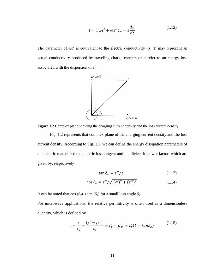
Fig. 1.2 represents that complex plane of the charging current density and the loss
current density. According to Fig. 1.2, we can define the energy dissipation parameters of
a dielectric material: the dielectric loss tangent and the dielectric power factor, which are
given by, respectively
tan 𝛿𝑒 = 휀′′ 휀′⁄
cos 𝜃𝑒 = 휀′′ √ (휀′)2 + (휀′′)2⁄
(1.13)
(1.14)
It can be noted that cos (θe) ≈ tan (δe) for a small loss angle δe.
For microwave applications, the relative permittivity is often used as a dimensionless
quantity, which is defined by
ε =휀
휀0=
(휀′ − 𝑗휀′′)
휀0= 휀𝑟
′ − 𝑗휀𝑟′′ = 휀𝑟
′ (1 − 𝑡𝑎𝑛𝛿𝑒) (1.15)
Figure 1.2 Complex plane showing the charging current density and the loss current density.
θe
δe
Jc=jωε’E
Jg=ωε”E
J

12
where ε is the complex permittivity, εr is the relative permittivity, ε0 is permittivity of free
space (8.854х1e-12 [F/m]), and δe is the dielectric loss angle.
Now, let us consider the magnetic response of a low-conductivity material. According to
Faraday`s inductance law
V = L𝑑𝐼
𝑑𝑡
(1.16)
The magnetization current Im:
𝐼𝑚 = −j𝑉
𝜔𝐿0
(1.17)
where V is the magnetization voltage, L0 is the inductance of an empty inductor, and ω is
the angular frequency. Under lossless conditions air inductor with a magnetic material with
a relative permeability (µr’) leads to
𝐼𝑚 = −j𝑉
𝜔𝐿0𝜇𝑟′
(1.18)
The relationship between the magnetization current and the voltage, as well as the
relationship between the magnetization current and the loss current (Ig) are shown in Fig.
1.3.
900
V
Im=-j (V/ω L0 µ’r) Im I
Igθ
δ
(a) (b)
Figure 1.3 The magnetization current in a complex plane (a) The relationship between the
magnetization current and the voltage (b) the relationship between the magnetization current and
the loss current.

13
The magnetic loss current is caused by energy dissipation during the magnetization
cycle. It is also in phase with magnetization voltage (V).
Now, let us consider the lossy situation in terms of the complex permeability.
For a dielectric case, we can obtain the total magnetization current by introducing a
complex permeability (µ= µ’-jµ’’) and a complex relative permeability (µr= µr’-jµr
’’):
μ =𝜇
𝜇0=
(𝜇′−𝑗𝜇′′)
𝜇0= 𝜇𝑟
′ − 𝑗𝜇𝑟′′ = 𝜇𝑟
′ (1 − tan(𝛿𝑚)) (1.19)
𝐼 = 𝐼𝑚 + 𝐼1 = −j𝑉
𝜔𝐿0𝜇𝑟= −
𝐽𝑉( μr’ − jμr’’)
𝜔(𝐿0 𝜇0⁄ )(𝜇′2 + 𝜇"2)
(1.20)
We can define the magnetic loss tangent and the magnetic power factor:
tan 𝛿𝑚 = 𝜇′′ 𝜇′⁄
cos 𝜃𝑚 = 𝜇′′ √ (𝜇′)2 + (𝜇′′)2⁄
(1.21)
(1.22)
where µ is complex permeability, µr is the relative complex permeability, µ0 is permeability
of free space (4πx1e-7 [H/m]), and δm is the magnetic loss angle.
In conclusion, the macroscopic electric and magnetic behavior of low-conductivity
materials is essentially obtained by permittivity and permeability. Energy absorption in
materials is due to their dielectric and magnetic properties, which depend on the imaginary
parts of the complex permittivity (εr= εr’-jεr
’’) and complex permeability (µr= µr’-jµr
’’). The
complex dielectric permittivity and magnetic permeability represent the dynamic dielectric
and magnetic properties of materials. The real components (εr’ and µr’) of the complex
dielectric permittivity and magnetic permeability denote the storage capability of electric

14
and magnetic energy. The imaginary components (εr” and µr”) of them represent the loss
of the electric and magnetic energy.
Propagation Parameters
There are two parameters to describe the propagation of electromagnetic waves in a
medium, which are the characteristic wave impedance (η) and the complex propagation
constant (γ). When a plane electromagnetic wave propagates with a velocity (υ) in the
positive z-direction, the characteristic impedance is defined as the ratio of the total electric
field to the total magnetic field in a z-plane. The characteristic wave impedance from the
permittivity and the permeability of a medium:
η = √𝜇 휀⁄ (1.23)
The characteristic wave impedance of free–space is η0= (µ0/ε0)1/2=376.7 ohm. The complex
propagation coefficient:
γ = α + jβ = 𝑗𝜔√𝜇휀 = 𝑗𝜔
𝑐√𝜇𝑟휀𝑟
(1.24)
where ω is the angular frequency, α is the attenuation coefficient, β (=2π/λ) is the phase
change coefficient, and λ is the operating wavelength in a medium, c=3x10⁸ m/s is the
wave velocity on free space.
1.3.2.2 The Parameters for High-Conductivity Materials
The complex propagation constant should be modified for a high conductivity material (a
metal) as

15
γ = α + jβ = 𝑗𝜔√𝜇휀√1 − 𝑗𝜎
𝜔휀
(1.25)
For a high conductivity material, we assume that the conducting current is much larger than
the displacement current (σ»ωε). Therefore, the displacement current term in Eq. (1.25)
can be ignored. Now, the complex propagation constant can be rewritten:
γ = α + jβ = 𝑗𝜔√𝜇휀√𝑗𝜎
𝜔휀= (1 + 𝑗)√
𝜔𝜇𝜎
2
(1.26)
The skin depth is a measure of the depth in which electromagnetic waves can penetrate into
the medium. For high-conductivity materials, the skin depth can be defined as
δ𝑠 =1
α= √
2
𝜔𝜇𝜎
(1.27)
The term meaning implies that the fields decay by an amount e-1 in a distance of a skin
depth (δs). For good conductors, it is very small distance (micrometers) at microwave
frequencies. Because of that, the behavior of a high-conductivity material at microwave
frequencies is determined by its surface impedance Zs:
Z𝑠 = R𝑠 + jX𝑠 =𝐸𝑡
𝐻𝑡= (1 + 𝑗)√
𝜔𝜇
2𝜎
(1.28)
where Ht is the tangential magnetic field, Et is the tangential electric field, Rs is the surface
resistance, and Xs is the surface reactance. σ is a real number for good conductors.
1.3.3 Classification of Materials
In this section, we explain further the electromagnetic behavior of typical materials,
including dielectric, magnetic, and composite materials. The knowledge of the underlying

16
mechanisms can help understand the measurement results and is important for the design
and application of these materials.
1.3.3.1 Dielectric Materials
A dielectric material is an insulator, which can be polarized by an applied electric
field. When an external electric field is applied to a dielectric material, the electric charges
do not flow through the material. However, certain changes in the charge configuration can
happen at the atomic scale. The parameter of permittivity is the key to the behavior of
dielectric materials. Fig. 1.4 represents a typical behavior of permittivity as a function of
frequency.
A material may have a variety of dielectric mechanisms or polarization effects,
which contribute to its overall permittivity [22]. A dielectric material has an arrangement
of electric charge carriers, which can be displaced by an external electric field. The material
Figure 1.4 Typical behavior of the permittivity for a hypothetical dielectric as a function of
frequency [20].

17
becomes polarized to compensate for the applied electric field such that the positive and
negative charges move in opposite directions. Different dielectric loss mechanisms can
contribute to dielectric behavior. Electronic and atomic polarizations, small orientation
(dipolar) polarizations, and ionic conductivity are the main mechanisms.
Electronic and atomic polarizations
Electronic polarization occurs in neutral atoms, when an external electric field displaces
the nucleus with respect to the surrounding electrons. Atomic polarization occurs when
adjacent positive and negative ions “stretch” under an applied electric field. Both
polarizations are similar nature. Fig. 1.5 [23] represents the behavior of permittivity in the
surrounding area of the resonant frequency (ω0).
A is the contribution of higher resonance to εr’ in the present frequency range. 2B/ ω0 is the
contribution of the present resonance to lower frequencies. These are the dominant
polarization mechanisms to determine the permittivity for many dry solids at microwave
Figure 1.5 The behavior of permittivity due to electronic or atomic polarization [23].

18
frequencies, even if the actual resonance occurs at a much higher frequency. If only these
two polarizations are exist, the materials are almost lossless at microwave frequencies.
Orientation (dipolar) polarization
A molecule is formed when atoms combine to share one or more of their electrons.
This rearrangement of electrons may cause an imbalance in charge distribution creating a
permanent dipole moment. These moments are oriented in a random manner in the absence
of an electric field so that no polarization exists. The electric field E will exercise a torque
T on each electric dipole, and the dipoles will rotate to align with the electric field causing
orientation polarization to occur (Fig. 1.6). If the field changes the direction, the torque
will also change.
The friction accompanying the orientation of the dipole will contribute to the
dielectric losses. The dipole rotation causes a variation in both εr’ and εr’’ at the relaxation
frequency which usually occurs in the microwave region. Water is an example of a
substance that exhibits a strong orientation polarization.
Ionic Conductivity
The measured loss of material can actually be expressed as a function of both dielectric
loss (erd’’) and conductivity (σ).
Figure 1.6 Dipole rotation, when an external field applied [22].

19
휀𝑟" = 휀𝑟𝑑
" +𝜎
𝜔휀0 (1.30)
At low frequencies, the overall conductivity can be made up of many different conduction
mechanisms, but ionic conductivity is the most prevalent in moist materials. er’’ is
dominated by the influence of electrolytic conduction caused by free ions which exist in
the presence of a solvent (usually water). Ionic conductivity only introduces losses into a
material. At low frequencies the effect of ionic conductivity is inversely proportional to
frequency and appears as a 1/f slope of the er’’ curve
Interfacial or Space Charge Polarization
It occurs when the motion of these migrating charges is impeded. The charges can
become trapped within the interfaces of a material. Motion may also be impeded when
charges cannot be freely discharged or replaced at the electrodes. The field distortion
caused by the accumulation of these charges increases the overall capacitance of a material
which appears as an increase in εr ’. Mixtures of materials with electrically conducting
regions that are not in contact with each other (separated by non-conducting regions)
exhibit the Maxwell-Wagner effect at low frequencies. If the charge layers are thin and
much smaller than the particle dimensions, the charge responds independently of the charge
on nearby particles. At low frequencies the charges have time to accumulate at the borders
of the conducting regions causing εr ’ to increase. At higher frequencies, the charges do
not have the time to accumulate and polarization does not occur since the charge
displacement is small compared with the dimensions of the conducting region. As the
frequency increases, εr’ decreases and the losses exhibit the same 1/f slope as normal ionic
conductivity. Many other dielectric mechanisms can occur in the low frequency region
20
causing a significant variation in permittivity. For example, colloidal suspension occurs if
the charge layer is of the same order of thickness or larger as the particle dimensions. The
Maxwell-Wagner effect is no longer applicable since the response is now affected by the
charge distribution of adjacent particles [23].
1.3.3.2 Magnetic Materials
In this part, we focus on magnetic materials with low conductivity because metallic
magnetic materials are rarely utilized as magnetic materials at microwave frequencies. At
microwave frequencies, the skin/ penetration depth of metals is about a few microns. The
interior of a metallic magnetic material does not respond to a microwave magnetic field.
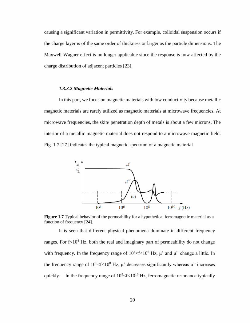
Fig. 1.7 [27] indicates the typical magnetic spectrum of a magnetic material.
It is seen that different physical phenomena dominate in different frequency
ranges. For f<104 Hz, both the real and imaginary part of permeability do not change
with frequency. In the frequency range of 104<f<106 Hz, µ’ and µ” change a little. In
the frequency range of 106<f<108 Hz, µ’ decreases significantly whereas µ” increases
quickly. In the frequency range of 108<f<1010 Hz, ferromagnetic resonance typically
Figure 1.7 Typical behavior of the permeability for a hypothetical ferromagnetic material as a
function of frequency [24].

21
arises. Above the f>1010 Hz, the magnetic properties of a material have not been fully
investigated.
In order to explain which mechanisms affect the magnetic losses for permeability
measurements, the loss mechanisms can be listed as:
Hysteresis Loss from irreversible magnetization. It is negligible in a weak
applied field.
Magnetic Resonance
Eddy Current Loss [25].
Hysteresis Loss
Fig. 1.8 shows that the hysteresis loop of a typical magnetic material. The domains are
randomly orientated at the starting point 0. Therefore, the net magnetic flux density is zero.
The magnetic flux density (B) increases with an increase in the magnetic field strength H,
as the domains close to the direction of the magnetic field grow. This continues until all
the domains are in the same direction as the magnetic field H and the material is saturated.
Figure 1.8 The Hysteresis Loop of a magnetic material [4].

22
The flux density reaches its maximum value Bm At the saturation state. When the magnetic
field strength is reduced to zero, the domains in the material turn to their easy-
magnetization directions close to the direction of the magnetic field H, and the material
retains a remanence flux density Br. The domains grow in the reverse direction once we
reverse the direction of the magnetic field. When the numbers of the domains in the H
direction and opposite the H direction are equal, the flux density becomes zero, the value
of the applied magnetic field is called coercive field Hc. Any further increase in the strength
of the magnetic field in the reverse direction results in further growth of the domains in the
reverse direction until saturation in the reverse direction is achieved. When this field is
reduced to zero, and then reversed back to the initial direction, we can get a closed
hysteresis loop of the magnetic material.
Magnetic Resonance
It is an important magnetic loss mechanism of magnetic materials. For most of
the magnetic materials, the energy dissipation at microwave frequencies (GHz) is
related to wall resonance and natural resonance [4].
1.3.3.3 Composite Materials
A composite material is made from two or more constituents, which have
significantly different physical and chemical properties. When the constituents
combine, they produce a new material with characteristics different from these of the
individual components. Composite materials usually consist of a host matrix and fillers.
The properties of a composite material are associated with the properties and fractions
(mass and/or volume) of the constituents, so the electromagnetic properties of

23
composites can be tuned up by varying the properties and fractions of the constituents.
The study of the electromagnetic properties of composite materials is very appealing
because of the potential of developing composites with expected (or desired)
electromagnetic properties. In this study, we are focused on composite materials in the
classifications of dielectric and magnetic constituents, which are used as a host matrix,
and fillers, respectively.
1.3.4 The Properties of Materials
The properties of materials can be classified into two categories: intrinsic and
extrinsic. Intrinsic properties of a material are independent of the size of the material. If
the electromagnetic properties of a material are associated with the geometry (or
geometrical structures) and size are called extrinsic.
1.3.4.1 Intrinsic Properties
Most of the electromagnetic properties discussed above are intrinsic properties.
They are controlled by their respective underlying mechanisms (not by geometries). The
intrinsic properties are described by the constitutive parameters and the corresponding
propagation parameters. As mentioned earlier in this chapter, electromagnetic waves can
propagate within low-conductivity materials. The constitutive parameter for low-
conductivity materials mainly consist of their permittivity, permeability and conductivity.
Additionally, the propagation parameters for low-conductivity materials mainly include
the wave impedance and the propagation constant.

24
1.3.4.2 Extrinsic Properties
The performance of electromagnetic materials/structures is also related to their
geometry and property. In order to ensure that the final products (or composite materials)
have the specified performance, both the intrinsic and the extrinsic properties need to
monitored during the fabrication process.
A typical example of extrinsic performance is given to explain why the geometry
(or size) in a RAM studied in this thesis is important for the microwave absorption
properties. The dissipation of energy is made by a relatively homogeneous specimen layer
backed by a ground plane (metal plate) (Fig.1.9).
The reflectivity of the layer depends on its thickness and the geometry for the
microwave absorption measurements, which will be explained in the following chapters.
In the design of the system, we have to consider the interferences between the reflections
at different interfaces, which are the first reflection and the second reflection, respectively.
The first reflection occurs when a part of incoming signal is reflected at the interference
between the free space (or air) and the specimen layer. The other part of the incoming
METAL
PLATE
Incident Wave
First Reflection
Second Reflection
d
Figure 1.9 The Schematic Illustration of a Waveguide measurement Setup to explain extrinsic
performance

25
signal propagates into the layer is partly attenuated by the lossy specimen and eventually
is reflected at the interface between the layer and the metal plate. That is the second
reflection, which after undergoing further attenuation comes out of the layer again. The
first reflection can be reduced by choosing a suitable wave impedance for the specimen;
the second reflection can be reduced by the loss within the specimen. Both factors
contribute to the overall reflection of the RAM configuration.

26
This page intentionally left blank
27
Chapter 2
Knitted Radar Absorbing Materials
(RAMs) Based on Nickel-Cobalt
Magnetic Materials

28
2. Knitted Radar Absorbing Materials (RAMs) Based on Nickel-
Cobalt Magnetic Materials
There has been a long-standing interest in the development of flexible, lightweight,
thin, and reconfigurable radar absorbing materials (RAM) for military applications such as
camouflaging ground-based hardware against airborne radar observation. The use of
polymeric Polyacrylonitrile (PAN) fabrics as a host matrix for magnetic metal nano-
particles either at the yarn-stage or after weaving the fabric for shielding and absorbing
applications has been described in the literature. In this chapter, the relative concentrations
of Nickel and Cobalt as well as the coating time are varied with a view to optimizing the
microwave absorption characteristics of the resulting PAN-based composite material in the
radar-frequency bands (X, Ku, and K).
2.1 Background & Literature Review
Bogush [26] has discussed the use of PAN fabrics as a host matrix for magnetic
NPs either at the yarn stage or after weaving the fabric for the RAM applications. He has
extensively discussed in his study how to deposit nano-structured materials on/over PAN
fabrics and to evaluate Ni and Co for their absorption properties over wide frequency
ranges (1-118GHz). However, there is no information about the relative amounts of Ni and
Co materials, an optimization criterion, or a characterization technique in his study. In our
experimental investigation, different relative concentrations of Nickel and Cobalt as well
as the coating time are used with a view to optimizing the microwave absorption
characteristics of the resulting knitted PAN fabrics-based composite material in the radar-
frequency bands (X, Ku, and K).

29
The development of electromagnetic (EM) wave absorbing and shielding nano-
structured materials has grown because of their use in the fabrication of thin, lightweight,
and flexible radar absorbers for military applications such as camouflaging ground-based
hardware against airborne microwave radar observation. The microwave absorption
properties are determined by the complex dielectric permittivity and the complex magnetic
permeability of the material and need to be tailored for maximum shielding/absorption
efficiency. Microwave absorbers based on composite materials are typically composed of
a polymeric dielectric matrix with conductive or magnetic filler particles of different
shapes and sizes [27]. There are many processes for coating the polymer surface with nano
metals such as vacuum deposition and electroless metal deposition method [28, 29]. The
electroless metal deposition method has a low cost, has no limitation on the shape and size
of the plated substrate, and is a low-temperature (< 100 0C) process with an industrial-scale
high throughput [26]. Deposition is performed from soluble metal salts.
This chapter presents an experimental study of flexible, lightweight, thin, and
reconfigurable radar absorbing materials derived from polymeric Polyacrylonitrile (PAN)
fabrics coated with highly conductive metals. High-volume fibers such as PAN offer high
flexibility and other desirable mechanical properties. Nickel and Cobalt were selected for
deposition because of their high stability and a relatively simple deposition procedure.
Polymers allow creation of numerous metallic clusters with different size and shape in the
pores of the material [30].
The s-parameters of the synthesized materials were measured in the X, Ku, and K
bands using a vector network analyzer (NA) in conjunction with a waveguide system
incorporating samples of the coated textiles. The electromagnetic constitutive parameters

30
were calculated from the s-parameters using the Nicolson-Ross-Weir technique [2, 4]. In
addition, the return loss (RL) of the samples is estimated from the computed complex
permittivity and permeability values.
2.2 Fabrication and Measurement
2.2.1 Fabrication of PAN Samples
First, all PAN fabric samples were cut to an appropriate size to fit in the
waveguides. The dimensions of the woven fabrics were 0.9x0.4, 0.6x0.3, and 0.4x0.17
inches for X, Ku, and K Bands, respectively. Second, the PAN fabric samples were cleaned
and dried in an oven at 40 0C. In the next step, the samples were subjected to surface
sensitization in a suitable solution. At that point, the samples were ready for electroless
deposition from solutions containing metal salts (total 25 % by wt.) in order to coat the
activated PAN surfaces for different durations. Finally, the samples were over-coated with
a liquid polymer of a low molecular weight to protect the underlying composite from
oxidation and corrosion. The coated fabric identification “codes” and the corresponding
deposition times are listed in Tables 1 and 2. TA1x and TA2x codes belong to Ni0.2Co0.8
and Ni0.8Co0.2 metal concentrations (%wt), respectively. The tables contain the fabric
codes, the coating times (minutes), the thickness of the fabrics (mm), the center frequency
(fr), and the bandwidth of the return loss (GHz).
The fundamental requirements of deposition bath can be listed as metal ions/their
concentration from producing soluble metal salts, reducing agent, complexing agent, bath
stabilizers (control of pH and temperature), and surfactant. In electroless deposition
method, metal ions are reduced by the action of a chemical reducing agent, which is simply
31
an electron donor. The metal ions are electron acceptors, which receive electrons generated
because of reducing agent oxidation reaction, which occurs at catalytic surface of the
substrate that typically contains nucleation sites of metals. It is an autocatalytic process,
which accelerates the electroless chemical reaction allowing oxidation of the reducing
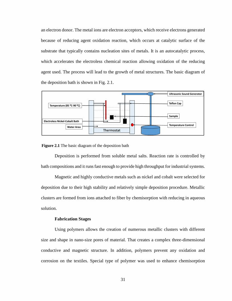
agent used. The process will lead to the growth of metal structures. The basic diagram of
the deposition bath is shown in Fig. 2.1.
Deposition is performed from soluble metal salts. Reaction rate is controlled by
bath compositions and it runs fast enough to provide high throughput for industrial systems.
Magnetic and highly conductive metals such as nickel and cobalt were selected for
deposition due to their high stability and relatively simple deposition procedure. Metallic
clusters are formed from ions attached to fiber by chemisorption with reducing in aqueous
solution.
Fabrication Stages
Using polymers allows the creation of numerous metallic clusters with different
size and shape in nano-size pores of material. That creates a complex three-dimensional
conductive and magnetic structure. In addition, polymers prevent any oxidation and
corrosion on the textiles. Special type of polymer was used to enhance chemisorption
ThermostatWater Area
Electroless Nickel-Cobalt Bath
Temperature (85 0C-90 0C)
Ultrasonic Sound Generator
Teflon Cap
Sample
Temperature Control
Figure 2.1 The basic diagram of the deposition bath

32
properties of PAN. Such polymer have been used in applications such as electromagnetic
shielding, anticorrosive coatings, manufacturing electrically conducting yarns [31] because
of their lightweight, conductivity, flexibility and low cost. Before starting the fabrication
process, the PAN textiles were modified after applying the special type of polymer, like
transformation, as described in [32].
a. Pre-Treatment
To clean industrial contaminants in/on PAN, PAN textile was washed with a non-
ionic detergent (pH=7) for 20 min. The amount of the detergent was 2% of deionized water.
Then, PAN is held in an ultrasonic Ethanol bath for 10 min. The ultrasonic bath of Ethanol
was intended to clean trapped contaminants between the knots or the corners of the knots
using the high frequency sound waves generated by the Sonorex Super 10P model
ultrasonic device. Ethanol in the crucible is squeezed and oscillated influenced by the
ultrasound waves, resulting in thousands of little bubbles during this process. The resulting
bubbles collapse at the bottom of the crucible. PAN textile is ready for sensitization stage
after the PAN textile washes with deionized water for 5 min and dried in an oven at 40 °C.
b. Sensitization
Some chemical bonds on the surface of PAN are broken and ready for a new
chemical bonding during this process. PAN textile was subjected to surface sensitization
in a suitable solution, which was a mixture of the surface sensitizer of Tin (II) Chloride
(SnCl2) with 5g/l and hydrochloric acid (HCl) (concentration 37% is equal to 37 g/mol or
12mol/L). Then the solutions was slowly agitated for 10 min at room temperature. The
sensitized textile was rinsed with deionized water for 5 min.

33
c. Activation
Metal nucleation will happen on this stage. The PAN textile was immersed in the
activator bath, which was composed of certain amount of Palladium (II) chloride (PdCl2),
HCl, and Boric acid (H3BO3) to obtain required conditions (pH=2, room temperature (25
0C) for 5 min) of surface activation. The ingredients and their respective amounts are listed
below.
TABLE I
COMPOSITIONS FOR ACTIVATION STAGE
After the activation stage, the textile needs to be cleaned with deionized water for 5 min.
d. Deposition
Deposition was performed from solutions containing metal salts, stabilizer and
reducing agent. Growth of metal structures was conducted using either autocatalytic
deposition or ion-molecular layering with stirring and correction of main solution
components: metal ions and reducing agent. The deposition baths for electroless Ni or Co
are composed mainly Nickel (II) Chloride 7-hydrate or Ni (II) Sulphate (the source of Ni)
and Cobalt (II) Chloride (the source of Co). The bath temperature is kept around 85 0C -
90 0C. The rate of pH is maintained in acid range for bath stability, but the generation of
hydrogen causes the pH value to decrease. To prevent this, alkaline salts of Na are usually
added. In this work, we used sodium hydroxide. Fig. 2.2 [33] shows the effect of solution
pH and bath temperature on the plating rate of electroless Ni deposits.
Compositions Amount of composition
Palladium (II) chloride (PdCl2) 0.3 g/l
Hydrochloric acid (HCl) 0.5 ml/l
Boric acid (H3BO3) 20 g/l

34
Metal Salts
Nickel (II) Chloride 7-hydrate, Ni (II) Sulphate are primary source of Ni. Cobalt
(II) Chloride is primary source of Co. For this work, two different compositions of Ni–Co
alloy, namely of 20/80 and 80/20 weight ratios. Amount of deposited metal was measured
via gravimetric technique [1].
Reducing Agent
Sodium hypophosphite employed as reducing agents in the case of formation of
cluster structure from nickel, cobalt or alloys. It was used in the chemical reduction of
Nickel-Cobalt from aqueous solutions.
The reduction of metal ions by hypophosphite involves two reactions (i)
hypophosphite ions are catalytically oxidized, (ii) Ni-Co ions are reduced at the catalytic
surface. A part of released hydrogen is absorbed onto the catalytic surface, which is called
an anodic reaction. Then, The Ni-Co ions at the surface of the catalyst is reduced by the
absorbed active hydrogen, which is called a cathodic reaction. Therefore, electroless
Figure 2.2 The effect of solution pH and bath temperature on the plating rate of electroless nickel
deposits.
0 20 40 60 80 100
0
2
4
6
8
10
12
14
P
latin
g R
ate
(m
/h)
Temperature (0
C)
3 4 5 6 7
2
4
6
8
10
12
14
Pla
tin
g R
ate
(m
/h)
pH
(a) (b)

35
deposition mechanism is related to anodic and cathodic reaction. Some absorbed hydrogen
reduces small amount of the hypophosphite to water, hydroxyl ion and phosphorus. For an
average efficiency of 37%, 1 kg of sodium hypophosphite is needed to reduce 200 g of Ni
or Co.
Stabilizers
Complexing agent: It is added to prevent the decomposition of solutions
and to control the reaction so that it occurs only on the catalytic surface. Complexing agents
are organic acids or their salts, added to control the amount of free electron (Ni or Co)
available for reaction. Therefore, Tri-sodium citrate is used as buffer and complexing
agent or pH control agent.
Ammonium Chloride is used as a flux, which is a flowing agent or
purifying agent. Fluxes may have more than one function at a time. For this work, it is used
to maintain low temperatures in the aqueous solution.
Sodium Hydroxide is utilized for pH regulation in aqueous solution. This
material is used since the solutions are cheaper and easier to handle. In small amounts,
some of Sodium Hydroxide may increase the rate of deposition. We suggest that it would
be better to use one or a couple drops of Sodium Hydroxide. We have to consider that
temperature, pH, metal ion concentration and concentration of the reducing agent control
the coating rate!
Eventually, all the metallized PAN textiles need to be rinsed with deionized water
at 40 0C for 20 min after deposition treatment.
Bath compositions and operating conditions are listed below.

36
Bath Compositions Descriptions Conditions
15 g/l Sodium hypophosphite
monohydrate
Reducing agent 40±1 0C,
pH=9,
Different coating
times. Iso-butanol Low-molecular weight
surfactant
8 g/l tri-sodium citrate Buffer and complexing
agent
A few drops Sodium Hydroxide Strong base, which react
with acids to form salts
18g/l ammonium Chloride To produce low
temperature in cooling
baths.
Metals Salts
15 g/l (for each salt) is preferred. The source of Ni and Co
e. Last-Treatment
High activity of metal particles and its oxidation by air oxygen in the presence of
residual water from plating solution requires additional protection that was created using
low molecular weight surfactants such as iso-butanol. Iso-butanol is a major industrial
solvent and key to the production of myriad chemicals and polymer intermediates. Bio-
based iso-butanol can serve as a key component in coatings, cleaning formulations, anti-
wear inhibitors and polymer intermediates while improving upon corporate sustainability
targets. The PAN textiles, after deposition process, were over coated with a liquid
surfactant of a low molecular weight iso-butanol. Then, the cleaned PAN textiles were
cured by steaming machine at 150 0C for 1 min. All textile samples were conditioned under
standard atmospheric pressure at 65±2% relative humidity and room temperature for at
least 24 h before evaluation or microwave measurements.

37
2.2.2 Experimental Methods and Measurement System
The crystal structure of the resultant composites was characterized using X-ray
diffractometer (Rigaku DMax-3C diffractometer with Cu Kα radiation of wavelength
λ=1.5406 Å) in the 2θ range of 35–90 degrees. Scanning electron microscopy (Philips
XL30 SPEG with scanning electron microscopy) was employed to observe the amount of
deposited material as nickel and cobalt filler particles. Finally, microwave absorption
measurements were carried out in the X, Ku, and K bands via the Transmission Line
Technique using a network analyzer (Agilent PNA E8364B) in conjunction with a
waveguide system incorporating samples of the coated fabric. The technique involves
placing the materials under measurement in a section of the waveguide and measuring the
two-port complex scattering parameters with the NA. The set up including the sample
holders with coated/uncoated samples is shown in Fig. 2.3.
Sample Holder
Network Analyzer
Waveguide (Rx)
Sample
Waveguide (Tx)
Plain textile in waveguide
Coated textile in waveguide
Figure 2.3 Waveguide Measurement System.

38
Calibration must be carried out with the sample holder holding the non-coated PAN
fabric sample before making measurements on the coated fabric samples. The material
must fit tightly in the sample holder in order to reduce the measurement uncertainty caused
by air gaps. After calibration was done, all samples were put into the holder and s-
parameters were measured by using the graphical user interface on the network analyzer.
Electromagnetic constitutive parameters for the coated fabrics (ε’, ε”, µ’, µ”) were
calculated from the measured s-parameters (S11 and S21) using the Nicolson-Ross-Weir
technique. Finally, the free-space reflection loss (RL) of the conductor-backed samples was
calculated from the following equation [34];
RL(dB) = −20log|(𝑍𝑖𝑛 − 𝑍𝑜)/(𝑍𝑖𝑛 + 𝑍𝑜)| (2.1)
Here, the effective input impedance of the radar absorbing material sample is
Zin=Z0√𝜇𝑟 휀𝑟⁄ tanh[(−j 2π c⁄ )𝑓𝑑√𝜇𝑟휀𝑟], where µr and εr are the measured relative
complex permeability and permittivity, respectively, c is the speed of light, f is the
frequency of operation, and d is the thickness of the sample. The results are discussed in
the following section.
2.3 Results and Discussion
2.3.1 Morphology and Crystal Structure Characterization
The coated fabrics were analyzed by using X-ray powder diffraction (XRD) and
Scanning Electron Microscopy (SEM). The XRD patterns of PAN fabrics shown in Fig.
2.4a and b confirm that the deposited particles are composed of Ni-Co alloys. Also, no
oxide peaks are detectable in the XRD patterns, indicating that the fabrics coated with Ni-
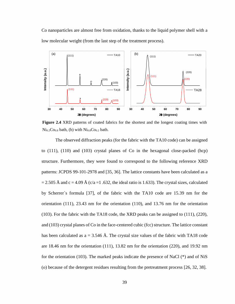
39
Co nanoparticles are almost free from oxidation, thanks to the liquid polymer shell with a
low molecular weight (from the last step of the treatment process).
The observed diffraction peaks (for the fabric with the TA10 code) can be assigned
to (111), (110) and (103) crystal planes of Co in the hexagonal close-packed (hcp)
structure. Furthermore, they were found to correspond to the following reference XRD
patterns: JCPDS 99-101-2978 and [35, 36]. The lattice constants have been calculated as a
= 2.505 Å and c = 4.09 Å (c/a =1 .632, the ideal ratio is 1.633). The crystal sizes, calculated
by Scherrer`s formula [37], of the fabric with the TA10 code are 15.39 nm for the
orientation (111), 23.43 nm for the orientation (110), and 13.76 nm for the orientation
(103). For the fabric with the TA18 code, the XRD peaks can be assigned to (111), (220),
and (103) crystal planes of Co in the face-centered cubic (fcc) structure. The lattice constant
has been calculated as a = 3.546 Å. The crystal size values of the fabric with TA18 code
are 18.46 nm for the orientation (111), 13.82 nm for the orientation (220), and 19.92 nm
for the orientation (103). The marked peaks indicate the presence of NaCl (*) and of NiS
(ο) because of the detergent residues resulting from the pretreatment process [26, 32, 38].
*
(103)
(220)
(111)
TA10(a) (b)
(220)
TA20
Inte
ns
ity
(a
.u.)
(111)
30 40 50 60 70 80 90
*
(111)
(220) (103)
TA18Inte
ns
ity
(a
.u.)
2(degrees)
30 40 50 60 70 80 90
(220)(111)
TA28
2 (degrees)
Figure 2.4 XRD patterns of coated fabrics for the shortest and the longest coating times with
Ni0.2Co0.8 bath, (b) with Ni0.8Co0.2 bath.

40
10 µmBefore deposition
(b)
2µmTA1x Series 0.5 min.
TA1x Series 8 min. 10µm
(c)
(d)
TA2x Series 0.5 min. 5µm
(e)
5µmTA2x Series 8 min.
(a)
Figure 2.5 SEM Micrographs of (a) Non-coated fabric, (b) TA1x series with the shortest coating
duration, (c) TA1x series with the longest coating duration, (d) TA2x series with the shortest
coating duration, (e) TA2x series with the longest coating duration.
41
The fabric samples coated for the shortest duration contain incomplete reduced
metal ion forms. The calculated lattice parameters of cobalt phase are in an agreement with
the published values [39, 40]. The characteristic diffraction peaks of the samples of Ni0.8
Co0.2, i.e, with higher Ni content (Fig. 2.4b), show the existence of a face centered cubic
(fcc) phase, in good agreement with references JCPDS 99-101-2978 and [41]. The crystal
size of the samples have been estimated to be in the range 12-26 nm. The lattice constant
(a = 3.526 Å) deviates only by 0.06% from the established value of fcc nickel (3.5238 Å)
[42].
SEM micrographs of PAN in Fig.2.5 show that clusters are distributed as particles
of different sizes and shapes and it appears that the fabric was coated with the deposited
material. The coating duration time varied from 0.5 min to 8 min for the TA1x (Ni0.2Co0.8)
and the TA2x (Ni 0.8Co0.2) Series. For the longest coating time, cracked layers were
observed for the TA1x (Ni 0.2Co0.8) Series. The roughness on the surface of the fabrics
increased because of the formation of nanoparticles. This is an important parameter for the
assessment of the success of the coating process.
2.3.2 Electromagnetic Constitutive Parameters
The electromagnetic constitutive parameters were calculated from the s-parameters
by the transmission line method using the Nicolson-Ross-Weir technique [4, 43]. Fig. 2.6
shows the real part of the relative permittivity, permeability, as well as dielectric and
magnetic loss tangents [tan (δe)and tan(δm)] of two different compositions of Ni-Co alloy,
namely of 20/80 and 80/20 weight ratios. Fig. 2.6a and 2.6c show that the ε’ (epsilon)' of
the coated fabrics gradually decreased for frequencies less than 20 GHz and tend to be

42
constant with nearly no variation throughout the 20-26.5 GHz range for both series of
coated fabrics [44-48]. It was observed that the real parts ε′ increase as the coating time
increases for both the TA1x and the TA2x series.
Fig. 2.6b and 2.6d show the real part of the permeability and the magnetic loss
tangent of the coated fabrics. The real part of permeability increases sharply up to 12 GHz,
then it tends to be constant around 1.2 and 1.3 for the TA1x and the TA2x series,
respectively, while the frequency is increased to 26.5 GHz.
8 12 16 20 24 284.7
4.8
4.9
5.0
5.1
5.2
(b)(a)
Rea
l P
art
of
Perm
itti
vit
y(')
Frequency (GHz) Frequency (GHz)
TA10
TA11
TA12
TA14
TA18
8 12 16 20 24 28
0.9
1.0
1.1
1.2
1.3 TA10
TA11
TA12
TA14
TA18
Rea
l P
art
of
Perm
ea
bil
ity(')
8 12 16 20 24 280.12
0.14
0.16
0.18
0.20
0.22 TA10
TA11
TA12
TA14
TA18
tan
(e
)
Frequency (GHz)
8 12 16 20 24 280.02
0.03
0.04
0.05
0.06
0.07
TA10
TA11
TA12
TA14
TA18
Frequency (GHz)
tan
(m
)
8 12 16 20 24 284.9
5.0
5.1
5.2
5.3
5.4
5.5
Rea
l P
art
of
Perm
itti
vit
y(')
TA20
TA21
TA22
TA24
TA28
(c)
Frequency (GHz)
8 12 16 20 24 28
0.9
1.0
1.1
1.2
1.3
Rea
l P
art
of
Perm
ea
bil
ity(')
TA20
TA21
TA22
TA24
TA28
(d)
Frequency (GHz)
8 12 16 20 24 280.26
0.28
0.30
0.32
TA20
TA21
TA22
TA24
TA28
tan
(e
)
Frequency (GHz)
8 12 16 20 24 280.05
0.06
0.07
0.08
TA20
TA21
TA22
TA24
TA28
tan
(m
)
Frequency (GHz)
Figure 2.6 Electromagnetic constitutive parameters with (a) Real part of permittivity and dielectric
loss for PAN coated with Ni0.2Co0.8, (b) Real part of permeability and magnetic loss for PAN coated
with Ni0.8Co0.2, (c) Real part of permittivity and dielectric loss for PAN coated with Ni0.8Co0.2, (d)
Real part of permeability and magnetic loss for PAN coated with Ni0.2Co0.8.

43
The dissipation factors are represented by dielectric loss (tan(δe) = εr”/ εr
’) in
Fig.2.4a and c. The magnetic dissipation factors, (tan(δm) = µr”/ µr
’) are shown in Fig. 2.4b
and d. The magnetic loss of the coated fabrics increases as the coating time increases. The
TA2x series fabrics have higher dielectric losses than the TA1x series fabrics. In addition,
it is apparent that, the dielectric losses are higher than the magnetic losses, which means
that the absorption originates mainly from the dielectric characteristics of the coated fabrics
rather than the magnetic characteristics.
2.3.3 Microwave Absorption Properties
The variation of the (computed) free-space return loss (RL) for the conductor-
backed PAN fabrics coated with various nano composites Ni-Co alloys of approximately
the same thickness (2 mm) are shown in Fig. 2.7.
The bandwidth (found to be approximately 2 GHz in this study) is defined here as
the frequency range, over which the return loss is less than -20 dB. The return loss was
calculated from a transmission-line-theory based computer simulation (MATLAB) using
the complex permittivity and the permeability values obtained from the measurements.
14 15 16 17 18
-35
-30
-25
-20
-15
-10
(a)
Retu
rn
Loss
(d
B)
Frequency (GHz)
TA10
TA11
TA12
TA14
TA18
14 15 16 17 18-40
-35
-30
-25
-20
-15
-10
(b)
TA20
TA21
TA22
TA24
TA28
Retu
rn
Loss
(d
B)
Frequency (GHz)
Figure 2.7 Frequency dependence of the RL of PAN fabrics containing Ni-Co alloys (a) Ni0.2Co0.8,
(b) Ni0.8Co0.2

44
The dips in the values of RL versus frequency imply low reflectivity (and good
absorption). As reported in the literature [49], the values of εr’ and εr
” vary with increasing
coating time, resulting in a variation in the depth of the RL troughs. Furthermore, the
difference between the TA1x and the TA2x series fabric samples is that RL troughs are
positioned above or below the 16 GHz reference frequency for the TA1x and the TA2x
series, respectively (Fig. 2.7a and 2.7b). This shows that the center frequency (fr) for the
minimum RL can be manipulated simply by changing the coating time and the Ni-Co
concentrations for the coated fabrics. The measurement results are summarized in Tables
II and III.
TABLE II
FABRICS CODES, CORRESPONDING DEPOSITION TIMES AND RESULTS FOR TA1X SERIES
Code Coating
Time
Thickness
d (mm)
fr (GHz) Return Loss
(dB)
Bandwidth (GHz)
(under -20 dB)
TA10 0.5 2.0189 16.39 -33.18 2.10 (15.32-17.42)
TA11 1 2.0299 16.59 -33.32 2.17 (15.59-17.76)
TA12 2 2.0278 16.50 -30.48 2.04 (15.49-17.53)
TA14 4 2.0209 16.58 -27.19 1.97 (15.67-17.64)
TA18 8 2.0248 16.78 -27.05 2.00 (15.82-17.82)
TABLE III
FABRICS CODES, CORRESPONDING DEPOSITION TIMES AND RESULTS FOR TA2X SERIES
Code Coating
Time
Thickness
d (mm)
fr (GHz) Return Loss
(dB)
Bandwidth (GHz)
(under -20 dB)
TA20 0.5 2.0188 15.91 -37.91 2.06 (14.89-16.95)
TA21 1 2.0298 15.69 -37.75 2.01 (14.75-16.76)
TA22 2 2.0276 15.55 -35.43 1.99 (14.61-16.62)
TA24 4 2.0206 15.70 -30.43 2.09 (14.74-16.84)
TA28 8 2.0196 15.79 -30.30 2.08 14.79-16.87)
We can compare the RAM performance that we fabricated with similar RAM performance in the
literature. Our collaborators had previously investigated coated PAN fabrics with different coating
times [8]. The microwave absorption curves show that microwave absorption properties depend on
45
the coating time. It is seen that the PAN fabrics with the shortest coating time are more effective
than the PAN fabrics with the longest coating time in terms of microwave absorption.
2.4 Conclusion
In this study, PAN fabrics coated with different weight fractions of Ni-Co alloys
have been investigated. XRD Patterns confirmed the crystal structures with the existence
of single Ni and Co phases (fcc for the Ni 0.8Co0.2 bath and hcp for the Ni0.2Co0.8 bath). As
expected, it was observed that, as the coating time increased, more metal salts resolved and
deposited on the surface of PAN fabrics in a solid state solution, and it was possible to
transition from crystal clusters to smooth metallic coatings on PAN fabrics. However, more
crystal clusters mean highly ordered metallic coatings, which are not desirable for the
broadband radar absorbing characteristics. The microwave absorption depends on coating
time. The TA2x series with the shortest coating time have the best RL. However, the
bandwidth for the RL values does not change significantly with the coating times. The
value of the dielectric tangent loss (tan δε) is higher than the value of the magnetic tangent
loss (tan δµ), which indicates that the absorption is more due to dielectric losses rather than
due to magnetic losses.

46
This page intentionally left blank

47
Chapter 3
Manganese and Zinc Spinel Ferrites
Blended with Multi-Walled Carbon
Nanotubes as Microwave Absorbing
Materials
48
3. Manganese and Zinc Spinel Ferrites Blended with Multi-Walled
Carbon Nanotubes as Microwave Absorbing Materials
Magnetic and dielectric materials can be blended to enhance absorption properties
at microwave frequencies, although the materials may have relatively weak attenuation
capabilities by themselves. The specific goal of this work is to enhance microwave
absorption properties of materials with interesting dielectric behavior by blending them
with magnetic materials based on transition metals. In this chapter, the synthesized
Mn1−xZnxFe2O4 (x = 0.0 and 1.0) spinel ferrite nanoparticles (MZF NPs) were blended with
commercial multi-walled carbon nanotubes (MWCNTs) in various proportions with a
binder matrix of paraffin. This simple and efficient process did not cause a significant
variation in the energy states of MWCNTs. MZF NPs were synthesized with a citric acid
assisted sol–gel method. Their electromagnetic characteristics and microwave absorption
properties were investigated. These properties were derived from the microwave scattering
parameters measured via the transmission line technique by using a vector network
analyzer (VNA) in conjunction with an X band waveguide system. The return loss (RL)
values of the samples were obtained from the electromagnetic constitutive parameters
(permittivity and permeability).
3.1 Background & Literature Review
Microwave absorbers are widely used in various defense and aerospace
applications, such as designing “stealth” aircraft, camouflaging ground-based military
assets against air-based radar surveillance, and constructing anechoic chambers (where the
radar signatures of aircraft and other targets are experimentally measured). The objective

49
of “stealth” and camouflage designs is to reduce the radar cross-section (RCS) of potential
targets, i.e., to make aircrafts, vehicles, or hardware systems less detectable to hostile radar
observation systems. Two approaches may be used to achieve a reduced RCS: shaping the
target so that the signal coming from the radar is guided in the desired directions (less
“backscatter”) and using radar-absorbing materials (RAMs) for attenuating the incoming
signal. In morphing applications, where large shape changes may be expected, the first
approach will have obvious limitations. Therefore, reducing RCS by means of
adaptive/smart structures incorporating RAMs becomes even more important. In general,
the design and application of RAMs has to be constrained by factors such as weight,
production costs, and maintenance [1]. Morphing concepts often involve the existence of
a suitable flexible skin, which has to be not only soft enough to permit shape changes but
also rigid enough to withstand loads [23]. This paper presents novel soft-skin RAMs, which
may have many potential applications including those in morphing scenarios.
Nonmetallic materials have been used in aircraft construction, most commonly for
wings, tails and control surfaces. Examples [3] of this include boron/epoxy horizontal tail
skins (used in the production of F14 aircrafts), boron/epoxy horizontal and vertical tail
skins (F15 aircrafts), graphite-epoxy horizontal and vertical skins and control surfaces (F16
aircrafts), graphite-epoxy wing, forward fuselage and control surfaces (Av-8B), and
graphite-epoxy control surfaces (Boeing 757). These materials can be integrated/covered
with suitable RAMs to enhance microwave absorption or to minimize reflection.
RAMs can be categorized into two types: dielectric and magnetic absorbers, which
means that the absorption is primarily due to their dielectric and magnetic characteristics,
respectively. The absorption by multi-walled carbon nanotubes (MWCNTs) is related to

50
their dielectric properties (complex permittivity), which depend on dielectric mechanisms,
such as electronic polarization and ion polarization. On the other hand, transition metals,
such as Fe, Ni, Co, Mn, and Zn, are magnetic materials, which rely on their magnetic
properties (complex permeability) to attenuate microwaves. However, both dielectric and
magnetic materials have relatively low absorption when they are used by themselves. It is
possible to enhance absorption characteristics when dielectric materials (MWCNTs) are
coated or blended with magnetic nanomaterials, such as transition metals or their ferrites,
which are known for their microwave absorption properties [6, 7].
Previous studies have used magnetic fillers, such as iron (Fe) [49], nickel (Ni)
nanowires [50], hybrid materials consisting of magnetite nanocrystals [6], carbonyl iron
particles [51], magnetite nanoparticle and hollow carbon fiber composites [52], carbon-
encapsulated cobalt (Co) nanoparticles [53], Co [54] , Ni and Co [55], zinc oxide whiskers
[56], in conjunction with CNTs [57] and ZnO [58]. We investigated manganese and zinc
spinel ferrite nanoparticles (MZF NPs) as filler materials because of their high flexibility,
high electrical resistivity, enhanced magnetic properties at radio frequencies, and their
super-paramagnetic behavior attributable to the nano-magnetic-sized particles. Moreover,
MZF NPs were blended in the MWCNTs through a simple and efficient process that did
not cause a significant variation in the energy states of MWCNTs. Our choice of MZF NPs
is consistent with the previous studies that used transition metals without MWCNTs, such
as Ni and Co [59], Co [60], nickel ferrite composites [61], NiCoZn spinel ferrites [62], Ni
and Zn spinel ferrites [63], and MnZn ferrite/rubber [64]. Gama, Rezende, and Dantas [64]
reported on the dielectric, magnetic and microwave absorption properties of rubber radar
absorbing materials depending on the Mn–Zn volume fractions (prepared by the usual

51
ceramic sintering method from a mixture of Fe2O3) and the thickness values of RAM in
the 2–18 GHz frequency range. Our work differs from [64] in that MZF NPs (synthesized
using a citric acid assisted sol–gel method) are used to implement the magnetic materials.
Desirable features of spinel ferrites, such as their enhanced magnetic properties in the radio
frequency region have attracted great interest in recent years [65]. Manganese ferrite
(MnFe2O4) and zinc ferrite (ZnFe2O4) are common spinel ferrite materials and they have
been used widely in microwave and magnetic recording applications [66]. We investigated
the effect of MWCNTs on magnetic, dielectric, and microwave absorption properties of
MnFe2O4 and ZnFe2O4 spinel ferrite RAMs according to their mass fractions.
To obtain the electromagnetic constitutive parameters (permittivity and
permeability), we measured the scattering parameters in the X band with an Agilent PNA
E8363B network analyzer (KEYSIGHT Technologies, Santa Rosa, CA, USA), in
conjunction with a waveguide system combining samples of MZF NPs blended with
MWCNTs. The electromagnetic constitutive parameters of the specimens were calculated
from the measured scattering parameters using the Nicolson-Ross-Weir algorithm [67].
The return loss (RL) values for each sample were additionally obtained from the calculated
complex permittivity and permeability values in order to assess their suitability as radar-
absorbing materials.

52
3.2 Materials and Methods
3.2.1 Materials
The binder matrix used in this work is paraffin. Commercial MWCNTs, supplied
by U.S. Research Nanomaterials, Inc., Houston, TX, USA, were used as a dielectric filler.
Their main characteristics, as provided by the supplier, are listed in Table IV [68].
TABLE IV
THE MAIN CHARACTERISTICS OF THE COMMERCIAL MULTI-WALLED CARBON NANOTUBES (MWCNTS)
ADOPTED AS FILLER.
MWCNT
Dimensions
Bulk
Density
Specific
Surface
Area
(m2/g)
Purity (wt %) Aspect
Ratio
Manufacturing
Method
Inside Diameter
5–10 nm,
Outside
Diameter 20–30
nm (from
HRTEM,
Raman), length
10–30 µm
(from TEM)
0.28
>110
(from
BET)
>95 (carbon
nanotubes from
TGA and TEM)
103 Chemical Vapor
Deposition
(CVD)
>97 (carbon
content)
Manganese and zinc spinel ferrites (MZF NPs) have been used as filler magnetic materials
after their synthesis by a citric acid assisted sol–gel method, which will be discussed in
detail in the next section.

53
Figure 3.1 Schematic illustration of: (a) The preparation process of manganese and zinc ferrite
nanoparticles (MZFs NPs); and (b) MZF NPs blended with multi-walled carbon nanotubes
(MWCNTs).
A schematic illustration of MZF NPs blended with MWCNTs in a paraffin host
matrix is presented in Fig. 3.1.
3.2.2 Preparation of Manganese and Zinc Ferrites (MZF)
Manganese and zinc ferrite particles in the present study were prepared by a citric acid
assisted sol–gel method shown in Figure 1. The sol–gel method has a wide range of
applications because of its high efficiency, large productivity, and low production
temperatures and costs. Conventional industrial methods for the manufacturing of ceramic
and glass need very high temperatures [66]. Therefore, in general, the sol–gel process is
known as soft chemistry. In addition, the sol–gel method is a multipurpose process where
the morphology, structure, and the composition of the final materials can be tuned by
altering the hydrolysis and condensation reaction proportions [69]. Here, we have listed
the steps of the sol–gel process, such as the homogeneous precursor solution with solid
20-30 nm 20-30 nm
7.5-10 nm
(b)(a)

54
materials, jellification, aging step, desiccation step, and densification step [70]. The
procedure of material preparation as reported by Demir et al. [71] was followed exactly
(for more details on material preparation, please consult [71]). A schematic representation
of the synthesis of Mn–Zn ferrite powder particles is given in Fig. 3.1a.
3.2.3 Preparation of Nanocomposite Samples
Six different MWCNTs-based magnetic nanocomposites were prepared with
various mass proportions using a binder matrix of paraffin through a simple and efficient
process. Obtaining homogeneous samples is crucial for reliable microwave measurements.
One important aspect in the use of nanoparticles in composites is a random dispersion
inside the matrix with the goal of obtaining homogeneous samples. Furthermore, mixing
filler nanoparticles within paraffin and eliminating air bubble formation inside the blend
are required to obtain a homogeneous dispersion. The fillers of MWCNTs and MZF NPs
were blended together in a proportion of 60 wt % (the total filling amount) with 40 wt %
of molten paraffin. In the present work, six absorber samples with different compositions
were prepared with the steps of 25%–50%–75% (three of them for the fillers of MnFe2O4,
and three of them for the fillers of ZnFe2O4). The proportion details for all RAM specimens
are shown in Table V. The process was carried out for the molten blend with the help of a
“magnetic stirrer”, which includes a heating plate and which uses ultrasound waves to
agitate particles. In the next step, the molten blend was poured into the sample holders,
which were the same size as the waveguide cross-section.
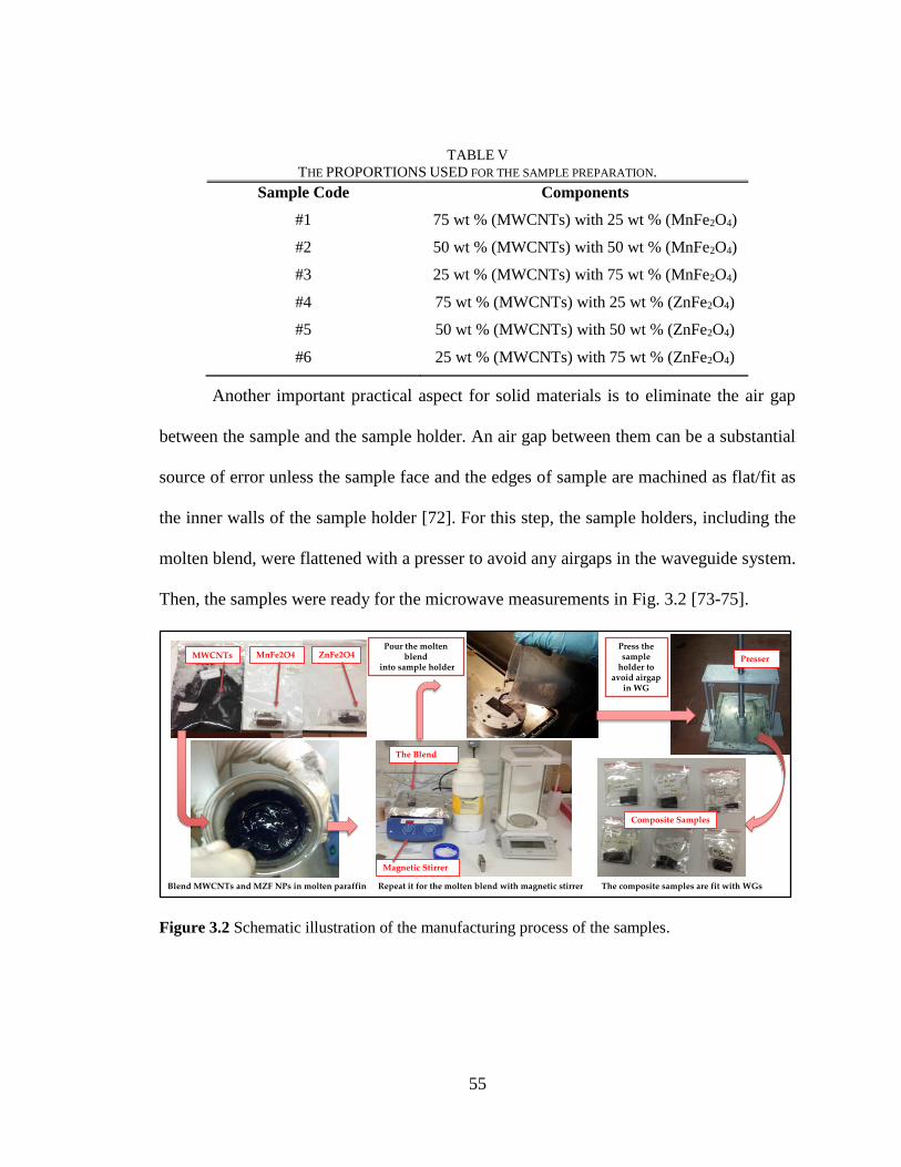
55
TABLE V
THE PROPORTIONS USED FOR THE SAMPLE PREPARATION.
Sample Code Components
#1 75 wt % (MWCNTs) with 25 wt % (MnFe2O4)
#2 50 wt % (MWCNTs) with 50 wt % (MnFe2O4)
#3 25 wt % (MWCNTs) with 75 wt % (MnFe2O4)
#4 75 wt % (MWCNTs) with 25 wt % (ZnFe2O4)
#5 50 wt % (MWCNTs) with 50 wt % (ZnFe2O4)
#6 25 wt % (MWCNTs) with 75 wt % (ZnFe2O4)
Another important practical aspect for solid materials is to eliminate the air gap
between the sample and the sample holder. An air gap between them can be a substantial
source of error unless the sample face and the edges of sample are machined as flat/fit as
the inner walls of the sample holder [72]. For this step, the sample holders, including the
molten blend, were flattened with a presser to avoid any airgaps in the waveguide system.
Then, the samples were ready for the microwave measurements in Fig. 3.2 [73-75].
Figure 3.2 Schematic illustration of the manufacturing process of the samples.
Magnetic Stirrer
The Blend
MWCNTs MnFe2O4 ZnFe2O4Pour the molten
blendinto sample holder
Press the sample
holder to avoid airgap
in WG
Composite Samples
Presser
Blend MWCNTs and MZF NPs in molten paraffin Repeat it for the molten blend with magnetic stirrer The composite samples are fit with WGs

56
3.2.4 Instrumentation
The crystalline structure of the resultant nanoparticles (MZF NPs) was
characterized with an X-ray diffractometer (Rigaku D/Max—3C using Cu Kα radiation,
Rigaku Innovative Technologies, Inc., Ettlingen, Germany) between 15 and 75 degrees in
the 2θ range with a step size of 0.1 (2θ).
Fourier transform infrared (FT-IR) spectra of MZF NPs were carried out on a
Bruker α-P by the attenuated total reflection (ATR) technique in transmission mode to
explore the nature of the chemical bonds formed in the range between 4000 and 400 cm−1.
By using a vibrating sample magnetometer (LDJ Electronics Inc., Model 9600,
Troy, MI, USA), Vibrating Sample Magnetometry (VSM) measurements were done. An
external field of up to 15 kOe at room temperature is applied to carry out the magnetization
measurements.
Scanning electron microscopy (SEM), was used to observe the amount of deposited
material as MZF NPs filler particles. By using a JEOL (JSM-7001F SEM-EDS-EBL, JOEL
USA, Inc., Peabody, MA, USA) scanning electron microscope, the surface morphology of
the samples was analyzed. SEM was operated at an accelerating voltage of 15 kV.
Energy-dispersive X-Ray spectroscopy (EDX) measurements were performed at 13
keV with INCA Instruments (Oxford Inca system, Oxford Co. Ltd., Belfast, UK).
Microwave S-parameter measurements were done in the 8.2–12.4 GHz frequency
range at room temperature using the transmission line technique with an Agilent PNA
E8364B network analyzer along with a waveguide system from Agilent (the specific
waveguide model is WR90, Santa Rosa, CA, USA).

57
3.3 Results and Discussion
3.3.1 Morphology and Crystal Structure Characterization
The crystal structure of nanoparticles was identified with X-ray powder diffraction
analysis, as shown in Fig. 3.3a and b. The particle sizes for both MnFe2O4 and ZnFe2O4
samples were calculated by the well-known Sherrer’s formula [76] using the full width at
half-maximum of intensity in the (400) plane of the spinel structure: L (nm) =
0.94λ/βcosθhkl. Here, L is the average crystallite size, β is the full width of the relevant
diffraction peak (FWHM), λ the X-ray wavelength (1.5418 Å), and θhkl is the angle of the
diffraction peaks. The experimental lattice constants (aexp) were calculated with the inter-
planner distances; dhkl-values and Miller indices (hkl) based on Bragg’s equation:
2 sinhkl hkln d (3.1)
( ) ( )2
2 2 2 2
exp1 hkld h k l a (3.2)
The diffraction peaks at 29.7°, 35.5°, 36.6°, 42.97°, 53.8°, 57.4°, and 62.65° could
be assigned from Fig. 3.3a, which correspond to (220), (311), (222), (400), (422), (511),
and (440) planes of MnFe2O4, respectively. As shown in Fig. 3.3a, the peaks were in good
agreement with the standard MnFe2O4 card (JCPDS cards No. 74-2403, 74-2402, 10-
0319), which indicate the samples had a face-centered cubic crystal structure. No
secondary impurity phase was detected, hence, the absence of any additional peaks
assigned to the graphite plane of MWCNTs. This means MWCNTs with ferrite nano-
particles are relatively coated. The broadening of the diffraction peaks indicates the nano-
crystalline nature of the materials. As shown in Fig. 3.3a, the XRD peaks marked (*) at
21.46° and 23.82° were caused by the paraffin because of its regular crystallization [37].

58
(a)
(b)
Figure 3.3 XRD patterns of samples fabricated with MZF NPs by blending commercial multi-
walled carbon nanotubes (MWCNTs) according to the mass fractions: (a) MWCNTs with MnFe2O4
samples; and (b) MWCNTs with ZnFe2O4 samples.
59
The calculated mean crystallite size value of MnFe2O4 is found to be about 22 nm.
The lattice constant (aexp) was calculated and found to be 8.4215 ± 0.0006.
The diffraction peaks at 30°, 35.3°, 35.5°, 42.9°, 53.2°, 56.9°, and 62.5° could be
assigned from Fig. 3.3b, which correspond to (220), (311), (222), (400), (422), (511), and
(440) planes of ZnFe2O4, respectively. As shown in Fig 3.3b, the peaks were in good
agreement with the standard ZnFe2O4 card (JCPDS cards No. 82-1042, 82-1012, 79-1150,
and reference code 01-089-4926), indicating the samples had face centered cubic crystal
structure. As shown in Fig. 3.3b, the XRD peaks marked (*) at 21.4° and 23.8° were caused
by the paraffin due to its regular crystallization. An additional peak, the peak marked (•),
was detected at 25.98° which corresponds to (002) planes of the MWCNTs. The calculated
mean crystallite size value of ZnFe2O4 found to be about 29 nm. The lattice constant (aexp)
was calculated and found to be 8.4306 ± 0.003 Å.
3.3.2 Fourier Transform Infrared (FT-IR) Analysis
The FT-IR spectra of the synthesized Mn1−xZnxFe2O4 NPs are presented with a step
size of 0.2 (x = 0:0.2:1) in Fig. 3.4, including the band positions of the investigated samples
(just MnFe2O4 and ZnFe2O4) shown in Table VI. The FT-IR spectra has been discussed
extensively in [71] and all details on the other step sizes of the FT-IR spectra are found
therein. According to the geometrical configuration of the oxygen nearest neighbors in
ferrites, the metal ions are located in two different sub-lattices. They are also designated as
tetrahedral and octahedral sites [77]. The specimens contained insignificant amounts of
organic residue, as shown in Fig. 3.4.

60
TABLE VI
VIBRATION FREQUENCIES OF THE SAMPLES
Sample Tetrahedral Octahedral
MnFe2O4 433 535
ZnFe2O4 430 528
Figure 3.4 Fourier transform infrared (FT-IR) spectra of Mn1−xZnxFe2O4 NPs for (a)
MnFe2O4; and (b) ZnFe2O4.
The characteristic peaks of MnFe2O4 for Mn–O, ZnO and Fe–O bond stretching
vibrations can be clearly observed at wave numbers 560 cm−1 in Fig. 3.4 [78, 79]. The
peaks at 1380 and 1600 cm−1 are attributed to the C=O stretching modes, respectively,
because of the coordination of the carboxylate groups of the citric acid by metal ions. It is
believed that the observed two peaks on the left of the 600 cm−1 wavenumber belong to
organic residues, which were used as fuel during the synthesis.
4000 3500 3000 2500 2000 1500 1000 500
(b)
Tra
ns
mit
tan
ce
(a
.u.)
Wavenumber (cm-1
)
(a) MnFe2O
4
(b) ZnFe2O
4
(a)

61
3.3.3 The Magnetization Measurements (VSM Analysis)
Magnetization curves (M versus H) of MZF NPs were measured at room
temperature with an applied field of ±15 kOe. Fig. 3.5b,c show the enlarged views in ±1.5
kOe demonstrating the hysteresis behavior for the synthesized MnFe2O4 and ZnFe2O4. The
values of Mr, Ms, and Hc were determined versus Zn mole concentrations depending on
Mn1−xZnxFe2O4 formula with a step size of 0.2 (0:0.2:1). Here, the values for just the
synthesized MnFe2O4 and ZnFe2O4 NPs have been reported. The values of saturation
magnetization (Ms), coercivity (Hc), and remnant magnetization (Mr) are determined from
hysteresis loops. They are listed in Table VII.
The results from the hysteresis loops indicated that all of the composite magnetic
spheres were magnetically soft at room temperature, when an external field was applied
(Fig. 3.5).
TABLE VII
MAGNETIC PROPERTIES OF THE SYNTHESIZED SPECIMENS
Sample Ms Hc Mr Mr/Ms
MnFe2O4 70.52 57 9.72 0.137
ZnFe2O4 35.90 50 4.03 0.112
Due to these values, it can be argued that all samples exhibited super-paramagnetic
behavior at room temperature. The observed Ms and Mr values of MnFe2O4 NPs were
higher than those for ZnFe2O4 NPs. It can be explained by noting that Zn has no net
magnetic moment. The values of Ms of MnFe2O4 are lower than the reported values for
bulk MnFe2O4 (80 emu/g) [80, 81]. Such behavior is ascribed to surface effects in
nanoparticles. The values of Ms of ZnFe2O4 particles was much higher than the bulk Ms

62
values of 5 emu/g [82]. Such behavior is related to cation distribution, which can change
from a normal spinel structure to a mixed spinel structure [71].
Figure 3.5 (a) Magnetic hysteresis loops of Mn1−xZnxFe2O4 NPs. The close up views for the M–H curves
of (b) MnFe2O4; and (c) ZnFe2O4.
3.3.4 The Surface Morphology of the Samples (SEM) Analysis
and The Energy Dispersive X-Ray (EDX)
SEM images of the nano-structured specimens are shown in Fig. 3.6, which
demonstrates the dispersion of MWCNTs particles and MnFe2O4 NPs as well as ZnFe2O4
NPs. The fillers were dispersed randomly in the host matrix. In addition, it is clearly seen
that some of MWCNTs were coated/filled with MZF NPs. This result agrees with the XRD
results, where the absence of any additional peaks implies that MWCNTs were coated with
spinel ferrite nanoparticles.

63
The EDX technique provides the effective atomic concentration of different
components in the top surface layers of solids. The energy dispersive X-ray (EDX) analysis
of the specimens, as shown in Fig. 3.7, was carried out to confirm the elemental
composition of the specimens. The EDX spectrum confirms the presence of Mn, Fe, C, and
O elementals, as well as Zn, Fe, C, and O elementals for the samples of MnFe2O4 with
MWCNTs and ZnFe2O4 with MWCNTs, respectively. The other minor peaks might be due
to the impurities in the starting materials. The relative atomic and weight abundance of Mn,
Zn, Fe, and O species are presented in the tables on each EDX graph. The atomic ratios of
Fe/Mn and Fe/Zn, found to be 2:1 by EDX analyses, confirmed the presence of MnFe2O4
and ZnFe2O4 nanoparticles on the MWCNT surfaces.
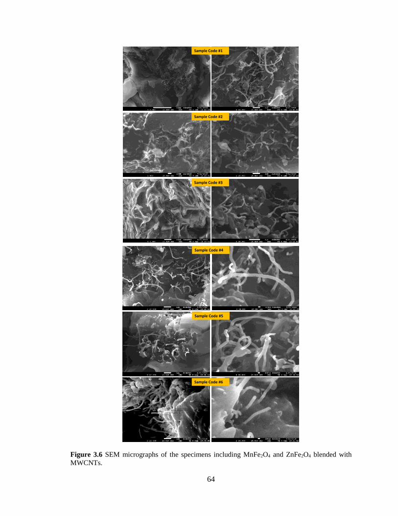
64
Figure 3.6 SEM micrographs of the specimens including MnFe2O4 and ZnFe2O4 blended with
MWCNTs.
Sample Code #1
Sample Code #2
Sample Code #3
Sample Code #4
Sample Code #5
Sample Code #6

65
3.3.5 Electromagnetic Constitutive Parameters
The values of electromagnetic complex permittivity and permeability were
calculated from the scattering parameters, such as S11 and S21, using the transmission line
method with the Nicolson–Ross–Weir algorithm [4]. Reflection coefficient Γ is given by
Γ = 𝐾 ± √(𝐾2 − 1) where 𝐾 = [(𝑆112 − 𝑆21
2 ) + 1]/2𝑆11. The transmission coefficient T is
(a)
(b)
Element Weight% Atomic%
C 93.24 94.91
O 6.61 5.05
Mn 0.06 0.01
Fe 0.09 0.02
MnFe2O4 w/MWCNTs
Element Weight% Atomic%
C 96.48 97.57
O 3.08 2.34
Fe 0.26 0.06
Zn 0.17 0.03
ZnFe2O4 w/MWCNTs
Figure 3.7 EDX spectrum of: (a) MnFe2O4 magnetic nanoparticles on multi-walled carbon
nanotubes; and (b) ZnFe2O4 magnetic nanoparticles on multi-walled carbon nanotubes.

66
given by 𝑇 = [(𝑆11 + 𝑆21) − Γ]/[1 − (𝑆11 + 𝑆21)Γ]. The permittivity and the permeability
are calculated [4] from:
( ) 2 2
0
1
1 11
r
c
(1.3)
( )
2
0
2 21 1
r
rc
(3.4)
2
2
1 1 1ln
2 d T
(3.5)
where λ0 is the wavelength of free-space; λc is the cut-off wavelength of the transmission
line. The schematic illustration of microwaves transmitting through, and reflecting from, a
sample in a waveguide transmission line is represented in Fig. 3.8.
Figure 3.8 Schematic illustration of electromagnetic waves transmitting through and reflecting
from a sample in a transmission line (such as a waveguide).
The complex constitutive parameters (dielectric permittivity and magnetic
permeability) denote the dielectric and magnetic properties of materials as RAMs. The real
components (εr’ and µr’) of the electromagnetic constitutive parameters represent the
storage capability of electric and magnetic energy. Energy loss in materials is due to the
imaginary part of the complex permittivity and complex permeability (εr” and µr”).
Magnetic losses are more effective and sensitive than dielectric losses for microwave
=0 =d
Thickness (d)
Einc
Erefl
Etrans
Port 1 Port 2

67
absorption. A small differences in permeability can even affect the microwave absorption
properties of the materials [83].
Fig. 3.9 and 3.10 show the real and the imaginary parts of the relative permittivity and
permeability of five different compositions of Mn or Zn ferrite and MWCNTs alloys,
namely in 25% increments of weight ratios.
(a)
(b)
8 9 10 11 12
0.0
0.2
0.4
0.6
0.8
1.0
1.2
2
3
4
5
6
7
Th
e R
eal P
art
(')
Th
e Im
ag
inary
Part
('')
MnFe2O
4
#3
#2
#1
Frequency (GHz)
MWCNTs
Permittivity Parameter
8 9 10 11 12
0.000
0.005
0.010
0.015
0.020
0.8
0.9
1.0
1.1
1.2
1.3
1.4
T
he R
eal P
art
(')
Th
e Im
ag
inary
Part
('')
Permeability Parameter
Frequency (GHz)
MWCNTs
#1
#2
#3
MnFe2O
4
Figure 3.9 Electromagnetic constitutive parameters with (a) the real and imaginary part of
permittivity for MWCNTs with MnFe2O4 samples; and (b) the real and imaginary part of
permeability for MWCNTs with MnFe2O4 samples (samples are color-coded).

68
(a)
(b)
As shown in Fig. 3.9a and 3.10a, the real part of the permittivity of the specimens
remained almost constant in the whole frequency range. The constancy means that there
was a dominant polarization, in which the oscillation of the electric dipole moments was
in phase or somewhat out of phase with the microwave frequencies [84]. Moreover, the
atomic and electronic polarizations may take place within a period shorter than the period
of a microwave signal. Both the direct current conductivity and the alternating current
8 9 10 11 12
0.0
0.2
0.4
0.6
0.8
1.0
1.2
3
4
5
6
7
T
he R
eal P
art
(')
Th
e Im
ag
inary
Part
('')
Permittivity Parameter
Frequency (GHz)
MWCNTs
#4
#5
#6
ZnFe2
O4
8 9 10 11 12
0.000
0.005
0.010
0.015
0.020
0.025
0.8
0.9
1.0
1.1
1.2
1.3
1.4
Permeability Parameter
Th
e R
eal P
art
(')
Th
e Im
ag
inary
Part
('')
Frequency (GHz)
MWCNTs
#4
#5
#6
ZnFe2
O4
Figure 3.10 Electromagnetic constitutive parameters with (a) the real and imaginary part of
permittivity for MWCNTs with ZnFe2O4 samples; (b) the real and imaginary part of permeability
for MWCNTs with ZnFe2O4 samples (samples are color-coded).
69
conductivity may cause the dielectric loss of the materials. It can be seen clearly by the
following equation:
( )"
0
dc
ac
(3.6)
It appears that the direct current conduction loss is inversely proportional to the
frequency; hence, the reason for the increase in ε″ for pure MWCNTs with decreasing
frequency at lower frequencies. In addition, it is noted that decreasing the loading amount
of MWCNTs in the composites, the values of the real and the imaginary part of permittivity
(ε′) decreased for both samples of MWCNTs with MnFe2O4 and ZnFe2O4.
Figures 9b, 10b, and 11 show the frequency dependence of the relative complex
permeability for the samples. It can be seen that the real part and the imaginary part of
permeability values (µ’ and µ″) lie in the ranges 0.8–1.3 and 0–0.02, respectively. The
small values of the latter suggest that the magnetic loss has a low contribution to
electromagnetic wave attenuation. In general, the magnetic loss of magnetic materials can
be predicted from magnetic hysteresis, eddy current loss, domain wall resonance, neutral
resonance, as well as exchange resonance. The eddy current loss is related to the electrical
conductivity and the thickness of the samples. It can be expressed by Xeddy [85]:
"2
2 02( ')eddyX d
f
(3.7)
where µ0 is the permeability value of a vacuum and σ is the electric conductivity of the
material. For the samples here, the eddy-current loss effect is negligible. That means the
eddy current loss has no significant effect in terms of microwave absorption properties.
It may be noted that the practical performance (RL value) of a RAM also requires
good impedance matching properties between air and the material (Section 3.3.6), which,
in turn, are associated with the resultant complex permittivity and permeability. Small

70
differences in permeability can even affect the microwave absorption properties of the
materials [86]. It will be seen later that the magnetic characteristics contributed well to the
RL values in Fig. 3.12.
(a)
(b)
The dielectric (tan(δε) = εr″/εr′) and magnetic (tan(δµ) = µr″/µr′) dissipation factors
are represented in Fig. 3.11a, and b. It is noted that the values of the magnetic dissipation
8 9 10 11 12
0.000
0.005
0.010
0.015
0.020
0.04
0.06
0.08
0.10
0.12
0.14
0.16
0.18
0.20
The DissipationFactors
tan
#1
MWCNTs
tan
Frequency (GHz)
#2
#3
MnFe2
O4
8 9 10 11 12
0.000
0.005
0.010
0.015
0.020
0.04
0.06
0.08
0.10
0.12
0.14
0.16
0.18
0.20
The DissipationFactors
tan
tan
Frequency (GHz)
MWCNTs
#1
#2
#3
ZnFe2
O4
Figure 3.11 The dielectric and magnetic dissipation factors with (a) MWCNTs with MnFe2O4
samples; (b) MWCNTs with ZnFe2O4 samples (samples are color-coded).

71
factors are generally less than the dielectric dissipation factors for the MWCNTs with
MnFe2O4 samples, which means that the absorption originates mainly from the dielectric
characteristics of MWCNTs with MnFe2O4 and ZnFe2O4 nanoparticles rather than the
magnetic characteristics.
In our case, dielectric mechanisms or polarization effects that contribute to its
overall complex permittivity may be used to explain why dielectric dissipation factors are
more significant than the magnetic dissipation factors. Once an electric field is applied,
positive and/or negative charges move in opposite directions, which contributes to the
dominant dipole polarization. The number of surface atoms with unsaturated bonds in Mn,
Zn, and Fe will increase as their sizes are at the nanoscale, resulting in an increase in dipole
polarization. The increased dipole polarization can contribute to the dielectric dissipation
factors (or dielectric loss). Another possible contribution to the dielectric dissipation is a
reasonable distribution of MZF NPs in MWCNTs. That can introduce extra interfaces
resulting in interfacial polarization. In addition, relaxation may occur at the MZF
NPs/MWCNTs interfaces, which contributes to the dielectric loss [87]. The space-charge
polarization can contribute an extra relaxation, resulting in an increase of the dielectric loss
to some degree [88]. For ferrite materials, it should be noted the value of ε′ is considerably
bigger than that of µ′, which is related to loss tangent factors [89].
The permeability graphs do not show an ordered structure as compare with the
permittivity parameters because Zn has no magnetic moment.

72
3.3.6 Microwave Absorption Properties
The return loss (RL) curves of the conductor-backed samples was obtained from
the following equation [2, 90]:
( )( )
0
0
( ) 20log in
in
Z ZRL dB
Z Z
(8)
Here, the effective input impedance of the sample is Zin =
Z0√μ𝑟 ε𝑟⁄ tanh[(−j 2π 𝑐⁄ )𝑓𝑑√μ𝑟ε𝑟], where µr and εr are the relative complex
permeability and permittivity, respectively, c is the speed of light, f is the frequency, and d
is the thickness of each sample.
The computed return loss (RL) for the various compositions of synthesized MZF
NPs in/on MWCNTs samples of approximately the same thickness (3 mm) is shown in Fig.
3.12. The lowest RL value and the bandwidth change with different loadings of manganese
and zinc spinel ferrite nanoparticles. A minimum RL of −56 dB at 11.41 GHz with a
bandwidth of 3.38 GHz (RL < −20 dB) was obtained in MWCNTs with MnFe2O4 NPs (x
= 0.0). A minimum RL of −42.06 dB at 11.05 GHz with an absorption bandwidth of 3.34
GHz (RL < −20 dB) was observed in MWCNTs with ZnFe2O4 NPs (x = 1.0). These results
are summarized in Table VIII.
TABLE VIII
SAMPLE CODES AND ABSORPTION RESULTS
Code fr
(GHz)
Return Loss (dB) Bandwidth (GHz) (under −20 dB)
Sample #1 10.44 −32.84 1.88 (9.42–11.3)
Sample #2 11.00 −41.20 2.2 (9.84–12.04)
Sample #3 11.41 −56.00 3.38 (9.7–13.08)
Sample #4 - - -
Sample #5 11.05 −42.06 3.34 (9.38–12.72)
Sample #6 10.55 −36.72 2.8 (9.00–11.80)

73
The table contains the sample codes, the center frequencies (fr), the values of
minimum achievable return loss (dB), and the corresponding bandwidths (GHz). It should
be noted that the dips in the values of RL versus frequency indicate low reflectivity (or a
good microwave absorption). Furthermore, the minimum RL values shifted to higher
frequencies and the bandwidths increased with an increasing amount of (manganese) ferrite
material in the blend (Samples #1, #2, and #3 in Fig. 3.12a). However, the minimum RL
values shifted to lower frequencies with an increasing amount of (zinc) ferrite material in
the blend (Samples #5 and #6 in Fig. 3.12b).
In comparison, our previous article [62] reported an RL of −38 dB with a
bandwidth of 2 GHz at 16 GHz for a purely magnetic absorbing material. In addition, the
results show that the dielectric (MWCNTs) materials and the magnetic materials (MZF
NPs) can mutually reinforce in terms of enhancing microwave absorption properties at
microwave frequencies. In order to investigate the claim that dielectric or magnetic
materials by themselves have relatively low RL values, dielectric samples (only MWCNTs
8 9 10 11 12
-60
-50
-40
-30
-20
-10
Re
turn
Lo
ss
(d
B)
Frequency (GHz)
MWCNTs
Sample #1
Sample #2
Sample #3
MnFe2O
4
(a)
8 9 10 11 12
-60
-50
-40
-30
-20
-10(b)
Re
turn
Lo
ss
(d
B)
Frequency (GHz)
MWCNTs
Sample #4
Sample #5
Sample #6
ZnFe2O
4
Figure 3.12 Frequency dependence of the return loss (RL) of MWCNTs with MZF NPs alloys;
(a) MWCNTs with MnFe2O4 samples; and (b) MWCNTs with ZnFe2O4 samples.

74
samples in the same wt % of total concentration of Samples #1, #2, and #3) were prepared
and the values of their RL versus frequency were computed. It was observed form Fig.
3.12a and 3.12b that dielectric or magnetic materials have low RL performance when they
are used by themselves.
The results of these composite samples showed that the microwave absorption is
enhanced once the dielectric and the magnetic materials are combined. In the literature,
there exist similar studies such as those for graphene oxide/strontium ferrite/polyaniline
(R-GOSF/PANI) [99]. The authors investigated samples of R-GOSF/PANI with different
weight ratios of GO and SF. Their results also exhibited the synergic effect between R-GO
(as dielectric materials) and strontium ferrite (as magnetic materials) in enhancing the
microwave absorption properties of the samples.
3.4 Conclusion
In this chapter, the synthesized Mn–Zn ferrites in/on MWCNTs with different
weight ratios were investigated. All synthesized samples exhibit super-paramagnetic
behavior at room temperature. XRD patterns are in good agreement with the JCPDS cards.
No secondary impurity phase was detected. The absence of any additional peaks attributed
to the graphite plane of MWCNTs, which indicated MWCNTs with ferrite nano-particles
are relatively coated. The return loss (RL) results show that the microwave absorption
properties of MWCNTs were enhanced by blending with magnetic materials. The
minimum RL value shifted to higher frequencies with an increasing amount of manganese
ferrite material in the blend. However, the minimum RL value tends to shift to lower
frequencies with an increasing amount of zinc ferrite material in the blend.

75
This page intentionally left blank

76
Chapter 4
The Measurement of Microwave
Absorption Characteristics of
Nanocomposites Using a Coaxial Line
Technique

77
4. The Measurement of Microwave Absorption Characteristics of
Nanocomposites Using A Coaxial Line Technique
Microwave absorption properties (MAP) of manganese soft spinel ferrite
(MnFe2O4) nanoparticles (MSF NPs) mixed with multi-walled carbon nanotubes
(MWCNTs) and molded as toroid-shaped pellets were experimentally studied using a
coaxial line technique in the frequency range of 2-18 GHz in this chapter. The coaxial line
technique was used because of the smaller sample size, a wider frequency range, and a
uniform cross section. The MAP were derived from the measured constitutive parameters,
according to the transmission line theory.
4.1 Introduction
It has been reported that, in applications requiring radar absorbing materials
(RAM), both dielectric and magnetic materials have relatively low microwave absorption
when they are used by themselves [91, 92]. It is possible to enhance absorption
characteristics when magnetic powder nanoparticles are blended with dielectric
nanomaterials [2]. For microwave absorption properties measurements, there exist several
different techniques such as waveguide, coaxial line, resonant cavity, and free-space[2, 59,
93-95]. In this study, we have adopted a reflection/transmission technique in a coaxial line
because of the smaller sample size, a wider frequency range, and a uniform sample cross
section. The coaxial line is especially suitable for solid (powder) materials. The method is
also preferable for measurements on powder samples because it uses less paraffin in the
sample than the waveguide method.

78
4.2 Fabrication and Measurement Setup
4.2.1 Preparation of Manganese Spinel Ferrite Nanoparticles
(MSF NPs) and the other additives of composites
Manganese and Zinc ferrite particles in the present study were prepared by a citric
acid assisted sol-gel method using a procedure reported by Demir et al. [71]and Teber et al
[2]. The steps of the sol-gel process are the formation of the homogeneous precursor
solution, sol, gel, aging, desiccation, and densification. MWCNTs were used as dielectric
materials in order to create conductive paths within composite samples. The MWCNTs
were purchased from US Research Nanomaterials, Inc., USA.
4.2.2 Fabrication of Nanocomposite Samples
For coaxial line measurements, the samples have to have a toroidal shape. The
material must fit tightly in the sample holder in order to reduce the measurement
uncertainty caused by air gaps. We designed our own manufacturing setup as shown in
Fig. 4.1a.
The dielectric and magnetic nanoparticles were blended in a crucible with
paraffin, and then the process was repeated for the molten blend with the help of a
magnetic stirrer, which includes a heating plate and uses ultrasound waves to agitate
particles. The molten blends were uniformly dispersed by stirring at 1000 rpm for 30
seconds. In the next step, the molten blend was poured into the sample holders, which
are the same size as a coaxial line cross section. The blends in the sample holder were
pre-cured at room temperature for half an hour. For the last step, the sample holders

79
including the pre-cured blends were flattened with a presser to avoid any air gaps in the
coaxial line system. The composite samples were fabricated into toroid-shaped samples
with an inner diameter of 3.5mm, an outer diameter of 7mm, and a thickness of 3mm.
A gold plated coaxial airline with a precision 7mm connector was used to hold the
sample [51, 96]. Then, the samples were ready for the microwave measurements of Fig.
4.1c.
Three different samples (MWCNTs-based magnetic nanocomposites of MSF NPs)
were fabricated by incorporating in a proportion of 80 wt. percentage (the total filling
amount) into 20 wt. percentage of a host matrix of molten paraffin. The filler materials
(ferrite particles and MWCNTs) were blended in various mass proportions with the steps
of 25-50-75%.
(a) (b)
(c)
MWCNTs
MnFe2O4
Powders
The Molded Sample
The Sample Holder
The Sample Rings
Figure 4.1 (a) The manufacturing mold system; (b) The powders of MWCNTs, manganese spinel
ferrites spinel ferrites; (c) The toroidal shape of the samples.
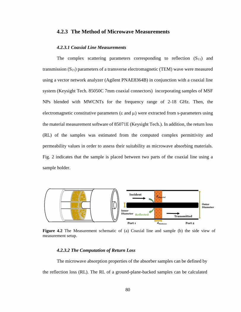
80
4.2.3 The Method of Microwave Measurements
4.2.3.1 Coaxial Line Measurements
The complex scattering parameters corresponding to reflection (S11) and
transmission (S21) parameters of a transverse electromagnetic (TEM) wave were measured
using a vector network analyzer (Agilent PNAE8364B) in conjunction with a coaxial line
system (Keysight Tech. 85050C 7mm coaxial connectors) incorporating samples of MSF
NPs blended with MWCNTs for the frequency range of 2-18 GHz. Then, the
electromagnetic constitutive parameters ( and ) were extracted from s-parameters using
the material measurement software of 85071E (Keysight Tech.). In addition, the return loss
(RL) of the samples was estimated from the computed complex permittivity and
permeability values in order to assess their suitability as microwave absorbing materials.
Fig. 2 indicates that the sample is placed between two parts of the coaxial line using a
sample holder.
4.2.3.2 The Computation of Return Loss
The microwave absorption properties of the absorber samples can be defined by
the reflection loss (RL). The RL of a ground-plane-backed samples can be calculated
Incident
ReflectedTransmitted
Zmaterial
dthickness
Outer Diameter
InnerDiameter
Port 1 Port 2
Figure 4.2 The Measurement schematic of (a) Coaxial line and sample (b) the side view of
measurement setup.

81
from the measured values of complex relative permittivity and permeability for the
given frequency and absorber thickness using the following equations:
( )
( )
1( ) 20log
1
in
in
ZRL dB
Z
(4.1)
while the normalized input impedance (Zin) is calculated by:
2tanhr
in r r
r
fdZ j
c
(4.2)
where f is the microwave frequency, d is the thickness of the sample, and c is the velocity
of electromagnetic wave in a vacuum. εr and µr are the complex relative permittivity and
permeability, respectively, which can be calculated by εr (= ε’- jε”) and µr (= µ’- jµ”).
4.3 Results and Discussion
4.3.1 The Structure and Morphology of the Samples and the
Energy Dispersive X-Ray (EDX)
The crystal phases of the resultant composites were investigated using the model of
Rigaku D/Max-3C using CuKα radiation (Rigaku Innovative Technologies, Inc.,
Germany) in the 2θ range of 20-800 with a step size of 0.1 (Fig. 4.3).
Fig. 4.4 shows the SEM images of the nano-structured samples, which
demonstrates the dispersion of MWCNTs particles and MnFe2O4 NPs. The morphology
features of the nanocomposites were characterized by scanning electron microscopy (SEM)
with the model of JSM-7001F SEM-EDS-EBL, JOEL USA, Inc., MA,USA, that operated
with an accelerating voltage of 5kV as well as the different magnification from 100x
(200µm) to 2000x (10µm).

82
SEM was examined observing the amount of deposited filler nanoparticles of
manganese spinel ferrites and MWCNTs. The fillers were dispersed randomly in the host
20 30 40 50 60 70 80
Inte
ns
ity
(a
.u.)
2 degrees
MnFe2O
4
(22
0)
(31
1)
(40
0)
(42
2)
(51
1) (4
40
)
29.70
35.50
42.970
53.80
57.40
62.650
D(nm) = 22aexp = 8.4215
JCPDS cards No: 74-2403, 74-2402, 10-0319FCC crystal structure
Figure 4.3 XRD patterns of samples fabricated with MZF NPs by blending MWCNTs.
Acc.V :5.00 kV Magn.:100x 200µm Acc.V :5.00 kV Magn.:250x 100µm
Acc.V :5.00 kV Magn.:1000x 20µm Acc.V :5.00 kV Magn.:2000x 10µm
Figure 4.4 The Surface Morphology of the specimens (MnFe2O4 blended with MWCNTs).

83
matrix. In addition, it is clearly seen that some of MWCNTs were coated/filled with MSF
NPs. This result agrees with the XRD results, where the absence of any additional peaks
implies that MWCNTs were coated with spinel ferrite nanoparticles.
Fig. 4.5 shows the EDX technique supplies the effective atomic concentration of
different constituents in the top surface layers of solids. The energy dispersive X-ray
(EDX) analysis of the specimens was carried out to confirm the elemental composition of
the specimens. Energy-dispersive X-Ray spectroscopy (EDX) measurements were
employed at 10 keV with INCA Instruments (Oxford Inca System, Oxford Co. Ltd., UK).
The EDX spectrum confirms the presence of Mn, Fe, C, and O elementals for the samples
of MnFe2O4 with MWCNTs. The other minor peaks might be due to the impurities in the
starting materials. The relative atomic and weight abundance of Mn, Fe, and Oxygen
species are presented in the table on EDX graph. The atomic ratios of Fe/Mn are found to
be 2:1 by EDX analyses, confirmed the presence of MnFe2O4 nanoparticles on the
MWCNT surfaces.
EDS kV:10 Mag:250 Takeoff:34.4 Live Time:30 Amp Time:6.4 Resolution:124.9
Element Weight % Atomic %
C K 33.39 52.8
N K 5.5 7.46
O K 22.23 26.39
Fe L 14.06 4.78
Mn K 24.81 8.58
Figure 4.5 The energy dispersive X-Ray (EDX) Spectrum of MnFe2O4 Magnetic Nanoparticles
on Multi-walled Carbon Nanotubes.

84
4.3.2 The Electromagnetic Properties of Composite Samples
The electromagnetic constitutive parameters were extracted using an Agilent PNA
E8364B network analyzer (Keysight Tech.) in conjunction with a coaxial line system
(Keysight Tech. 85050C 7mm coaxial connectors) at 2.4-18 GHz frequency range at room
temperature. The real (εr’ and µr’) and the imaginary part (εr” and µr”) of relative complex
permittivity and permeability as well as the dielectric loss tangent (tan (δε) =εr”/εr’) and the
magnetic loss tangent (tan (δµ) =µr”/ µr’) for nano-structured composites were extracted
with the help of the software (85071E Keysight Tech.), pre-installed in the network
analyzer. The real part of relative complex permittivity and permeability are associated
with the storage capability of electric and magnetic energies. The ε″ and μ″ are associated
with energy loss within materials, resulting from dielectric and magnetic mechanisms such
as conduction, resonance, interfaces, relaxation and atomic, electronic and/or dominant
polarization.
The relative permittivity real part (ε′), the relative permeability real part (μ′), the
dielectric loss tangent (tan δε = ε″/ε′), and the magnetic loss tangent (tan δμ = μ″/μ′) of
manganese spinel ferrites blended with MWCNTs with different weight percentages are
presented in Fig. 4.6. The weight percentages are namely in 25% increments of weight
ratios (Table IX).
TABLE IX
THE PROPORTIONS USED FOR THE SAMPLE (MWCNTS WITH MSF NPS) PREPARATION
Sample Code Proportions
1 75 wt % (MWCNTs) with 25 wt % (MnFe2O4)
2 50 wt % (MWCNTs) with 50 wt % (MnFe2O4)
3 25 wt % (MWCNTs) with 75 wt % (MnFe2O4)

85
In Fig. 4.6a and 4.6b, the ε′ values of the samples slightly decrease in the range of
10.4−1.1. The dielectric tangent loss slightly decreases in the range of 0.22-0.04 within the
frequency range 2.0-8.3 GHz. It increases in the range of 0.04-0.16 within the frequency
range 8.3-12.5 GHz. The dielectric tangent loss of the samples in the rest of the
frequency range exhibits almost a constant value with only a small fluctuation. The
constancy in the values of the real part of permittivity suggests that there was a dominant
polarization, in which the oscillation of the electric dipole moments was in phase or
somewhat out of phase with the microwave frequencies [96].
2 4 6 8 10 12 14 16 18
0.02
0.04
0.06
0.08
0.10
0.12
0.14
0.16
0.18
0.20
0.22
0.24
0.26
0.28
0.30
0.32
Ta
ng
en
t L
os
s (
tan(
"
')
Frequency (GHz)
75% wt. MWCNT w/ 25% wt. MnFe2O
4
50% wt. MWCNT w/ 50% wt. MnFe2O
4
25% wt. MWCNT w/ 75% wt. MnFe2O
4
2 4 6 8 10 12 14 16 18
0.8
0.9
1.0
1.1
1.2
Re
al Im
ag
ina
ry o
f P
erm
ea
bilit
y (')
Frequency (GHz)
75% wt. MWCNT w/ 25% wt. MnFe2O
4
50% wt. MWCNT w/ 50% wt. MnFe2O
4
25% wt. MWCNT w/ 75% wt. MnFe2O
4
(a) (b)
(c) (d)
2
4
6
8
10
2 4 6 8 10 12 14 16 18
Sample 1
Sample 2
Sample 3
Re
al P
art
of
Pe
rmit
tiv
iy ('
)
Frequency (GHz)
2 4 6 8 10 12 14 16 18
0.000
0.002
0.004
0.006
0.008
0.010
0.012
0.014
0.016
0.018
0.020
Sample 1
Sample 2
Sample 3
Ta
ng
en
t L
os
s (
tan(
"
')
Frequency (GHz)
Figure 4.6 The electromagnetic constitutive parameters (a) the relative real part of permittivity (b) The
Dielectric tangent loss of the samples, (c) the relative imaginary part of permeability (d) The Magnetic
tangent loss of the samples, resulting from MnFe2O4 magnetic nanoparticles on multi-walled carbon
nanotubes.

86
As demonstrated in Fig. 6c and d, we can observe that the µ′ values of the samples
slightly decreased in the frequency range of 2-10 GHz, whereas its values increased
between 10-18 GHz. The μ″ values (or tan δμ) of the samples indicate broad resonance
peak in the whole frequency range, which is related to the small size effect, surface effect,
and spin wave excitations [97].
It is observed that the tan δε values are higher than tan δμ, suggesting that the
magnetic loss is low. MWCNTs are often used as an additive coating with manganese
spinel ferrites to increase its conductivity [98]. According to the free-electron theory,
increased conductivity of a composite could result in strong dielectric loss, and thus, the
blend of MWCNTs and MSF NPs show a stronger dielectric loss in 2−18 GHz.
4.3.3 Microwave Absorption Properties
First, the results obtained by the previous waveguide1 and the present coaxial-
line methods over the common frequency range (8-12 GHz) are compared below in Fig.
4.7 and Table IX and show good agreement.
TABLE X
THE MICROWAVE ABSORPTION RESULTS
Code fr (GHz) Return Loss (dB) Bandwidth (under −20 dB)
Present
Work
Previous
Work
Present
Work
Previous
Work
Present
Work
Previous
Work
1 10.08 10.44 −34.07 -32.84 1.98 GHz 1.88 GHz
2 11.00 11.00 −45.16 -41.20 2.55 GHz 2.20 GHz
3 11.26 11.41 −53.31 -56.00 3.49 GHz 3.38 GHz

87
Fig. 4.8 presents the calculated return loss (RL) of the samples for the various
compositions of additives over the frequency range 2-18 GHz. The samples thickness
are approximately the same thickness (3 mm). It can be observed that the plots of RL
versus frequency indicate good microwave absorption. The minimum RL values shifted
to higher frequencies and the bandwidths increased with an increasing amount of
manganese ferrite material in the mixture. The lowest RL value and the bandwidth
change with different loadings of manganese and zinc spinel ferrite nanoparticles. A
minimum RL of −53.31 dB at 11.26 GHz with a bandwidth of 3.49 GHz (RL < −20 dB)
was obtained in MWCNTs with MnFe2O4 NPs.
8 9 10 11 12 138 9 10 11 12 13
-55
-50
-45
-40
-35
-30
-25
-20
-15
Sample 1 (from Ref.1)
Sample 2 (from Ref.1)
Sample 3 (from Ref.1)
Re
turn
Lo
ss
(d
B)
Frequency (GHz)
Sample 1 (Present Work)
Sample 2 (Present Work)
Sample 3 (Present Work)
Figure 4.7 Comparison Return Losses of Coaxial Line and Waveguide Measurements in the
frequency range of 8-12 GHz.

88
These comparison results are summarized in Table X, including the sample
codes, the center frequencies (fr), the values of minimum achievable return loss (dB),
and the corresponding bandwidths (GHz).
4.4 Conclusion
Because of both dielectric and magnetic contributions to microwave absorption
properties at microwave frequencies, the composite samples exhibited desirable
microwave absorption properties in terms of the minimum RL values and the broad
absorption bandwidths. The minimum RL value tends to shift to higher frequencies with
an increasing amount of manganese ferrite material in the mixture.
2 4 6 8 10 12 14 16 18
-60
-50
-40
-30
-20
-10
Bandwidth = 3.49 GHz
Return Loss(dB) = - 53.31
Re
turn
Lo
ss
(d
B)
Frequency (GHz)
Sample#1
Sample#2
Sample#3
fr(GHz) = 11.26
fr(GHz) = 11.00
Return Loss(dB) = - 45.16
Bandwidth = 2.55 GHz
fr(GHz) = 10.08
Return Loss(dB) = - 34.07
Bandwidth = 1.98 GHz
Figure 4.8 Return Loss versus frequency of MWCNTs with MSF NPs alloy with Coaxial Line
Technique.

89
5. Conclusion of Thesis
This work focused on developing radar absorbing materials (RAMs) based on nano-
structured magnetic materials with the goal of contributing to a better understanding of the
applications of flexible, reconfigurable, lightweight RAMs, which are camouflaging
ground-based hardware against hostile airborne radar observation and enhancement of
microwave absorption properties of the RAMs.
First, Polyacrylonitrile (PAN) textiles coated with different weight fractions of Ni-
Co alloys using electroless metal deposition method are investigated. Deposition is
performed with soluble metal salts. Reaction rare is contrilled by bath compositions and it
runs fast enough to provide high throughput for industrial systems. Magnetic and higly
conductive metals such as nickel and cobalt were selected for deposition due to their high
stability and relatively simple deposition procedure. Metallic clusters are formed from ions
attached to fiber by chemisorption with reducing in aqueous solution. XRD results
confirmed the crystal structures with the existence of single Ni and Co phases, which are
face-centered cubic (fcc) for the Ni0.8Co0.2 bath and hexagonal close-packed (hcp) for the
Ni0.2Co0.8 bath. As expected, it was observed that, as the coating time increased, more
metals resolved and deposited on the surface of PAN textiles in a solid state solution, and
it was possible to transition from crystal clusters to smooth metallic coatings on PAN
textiles. However, more crystal clusters mean highly ordered metallic coatings, which are
not desirable for the broadband radar absorbing characteristics. The microwave absorption
depends on coating time.
Second, Manganese and Zinc ferrites are synthesized using a citric acid assisted
sol-gel method. Mn-Zn ferrites in/on MWCNTs with different weight ratios were
90
investigated to enhance microwave absorption properties (low reflection). All synthesized
samples exhibited super-paramagnetic beahvior at room temperature as expected. XRD
patterns are in good agreements with the JCPDS cards in the literature. No secondary
impurity phase was detected. The return loss (RL) results indicated that microwave
absorption of MWCNTs were enhanced by blending magnetic materials as expected. The
significant finding of minimum reflection values shoed that the microwave absorption is
about 99.99%.
Then, the microwave absorption properties of Mn-Zn ferrites in/on MWCNTs were
measured using non-resonant methods including a waveguide and a coaxial line techniques
in order to cross-validate the absroption results. The scattering parameters (s-parameters)
of the RAMs were measured in the radar frequency bands by using a network analyzer.
The electromagnetic constitutive parameters were computed from the measured s-
parameters using Nicolson-Ross-Weir Algorithm (NRW) with the help of a MATLAB
code. In addition, the return loss of the RAMs is estimated from the computed permittivity
and permeability values.
The experimental results presented in this thesis are expected to encourage
further development of magnetic nano-particle coated textile absorbers for broadband
microwave absorber applications and to support a promising role for MWCNTs blended
with ferrite nano-particles for broadband applications.
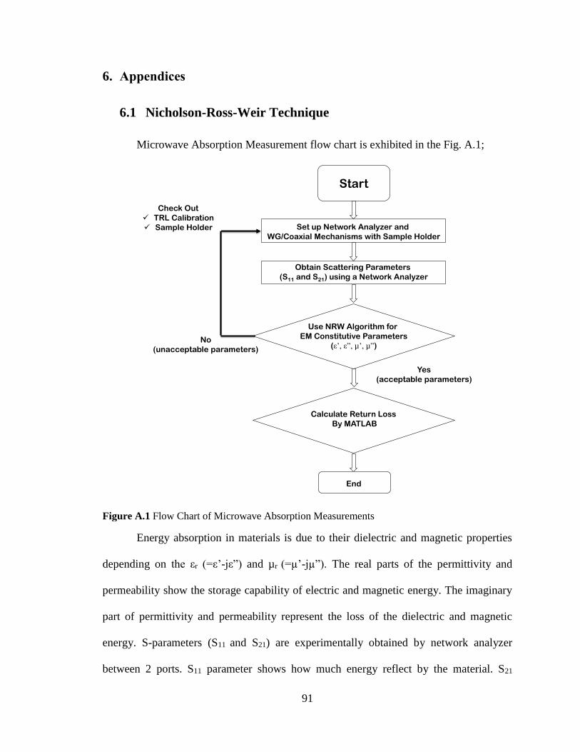
91
6. Appendices
6.1 Nicholson-Ross-Weir Technique
Microwave Absorption Measurement flow chart is exhibited in the Fig. A.1;
Energy absorption in materials is due to their dielectric and magnetic properties
depending on the εr (=ε’-jε”) and µr (=µ’-jµ”). The real parts of the permittivity and
permeability show the storage capability of electric and magnetic energy. The imaginary
part of permittivity and permeability represent the loss of the dielectric and magnetic
energy. S-parameters (S11 and S21) are experimentally obtained by network analyzer
between 2 ports. S11 parameter shows how much energy reflect by the material. S21
Check Out
TRL Calibration
Sample Holder
No
(unacceptable parameters)
Yes
(acceptable parameters)
Start
Set up Network Analyzer and
WG/Coaxial Mechanisms with Sample Holder
Obtain Scattering Parameters
(S11 and S21) using a Network Analyzer
Use NRW Algorithm for
EM Constitutive Parameters
(ε’, ε”, µ’, µ”)
Calculate Return Loss
By MATLAB
End
Figure A.1 Flow Chart of Microwave Absorption Measurements

92
parameter means how much energy pass through the material. Those two parameters are
related to complex permittivity and permeability. It will be explained the measurement and
calculation process in this flow chart in detail. First, we set up a vector network analyzer
in conjunction with waveguide system including the samples. Before making microwave
measurements we have to do calibration. It allows TRL calibration for this measurement.
Thru calibration is to connect directly Port1 and Port2, Reflect Calibration is to connect
metal plate with a high reflection coefficient to each port. Line calibration is to insert a
short length of transmission line between port 1 and port 2. Then, It is followed the flow
chart steps. NRW algorithm is used to calculate electromagnetic constitutive parameters.
Then if we get acceptable EM constitutive parameters. Later, we keep going to calculate
RL by MATLAB code. If not, we have to check it out the calibration and the sample holder
if there is airgap between the sample and sample holder.
Nicholson-Ross-Weir (NRW) technique provides a direct calculation of both the
complex relative permittivity and permeability from scattering parameters. The technique
is applicable for waveguide and coaxial line methods. The measurement of reflection and
transmission coefficient requires all four parameters of S11, S21, S22, and S12 or a pair of
S11, S21 of the material under the test (MUT) to be measured [4]. The procedure for the
NRW conversion process:
End
2 2
11 21
11
1
2
S Sx
S
2
2 2 2
0
*1 1 1 1ln
2
r r
c L T
Use
S Parameters
S11 & S21
Calculate
Reflection
Coefficient
Calculate
Transmission
Coefficient
Calculate
Permeability
Calculate
Permittivity
2 1x x
Check out lΓl<1
( )11 21
11 211
S ST
S S
( )
1
2 2
0
1
1 11
r
c
22
0
2
1 1 1ln
2r
r c L T
L :thickness of sample
Figure A.2 Computation Steps of Nicholson-Ross-Weir Algorithm

93
The S11 and S21 parameters can be directly obtained by a vector network analyzer (VNA).
( )( )
( )( )
2 2
11 212 2 2 2
1 1
1 1
T TS and S
T T
(A.1)
The reflection coefficient can be deduced as 2 1x x where 1 is required for
finding the correct root and
2 2
11 21
11
1S Sx
S
(A.2)
X factor can be defined by reflection coefficient (Γ);
(A.3)
The transmission coefficient can be written by
11 21
11 211 ( )
S ST
S S
(A.4)
The permeability is given as
2 2
0
1
1 1(1 )
r
c
(A.5)
where λ0 is free space wavelength and λc is cut-off wavelength of the transmission line
section, and for a coaxial line λc=ꭃ.
2
2 2 2
0
*1 1 1 1ln
2
r r
c L T
(A.6)
The permittivity can be defined as
( )( ) ( )
( )( )( )
( )
2
1
12
11
12
11
12
1
2
)(1
2
2
22
2
222
2
2222
11
2
11
2
21
K
T
T
T
TT
T
TTK
S
SSKx

94
( ) ( )
2
0
2 21 1r
r c
(A.7)
6.2 Microwave Measurement System
6.2.1 A Vector Network Analyzer and Its Principles
A vector Network Analyzer (VNA) is an instrument that measures network
parameters of electrical networks as a measurement of the reflection and/or transmission
through a material with the help of its physical dimensions, according to the transmission
line theory [25, 75]. That provides the information to characterize permittivity and
permeability of a material.
A VNA consists of a signal generator, a receiver and a display. The generator sends
a signal at a single frequency to the material. The receiver is tuned to that frequency to
detect the reflected/transmitted signals from the material. The measured reaction produces
Figure A.3 The Diagram of A Vector Network Analyzer (VNA)
(a) (b)
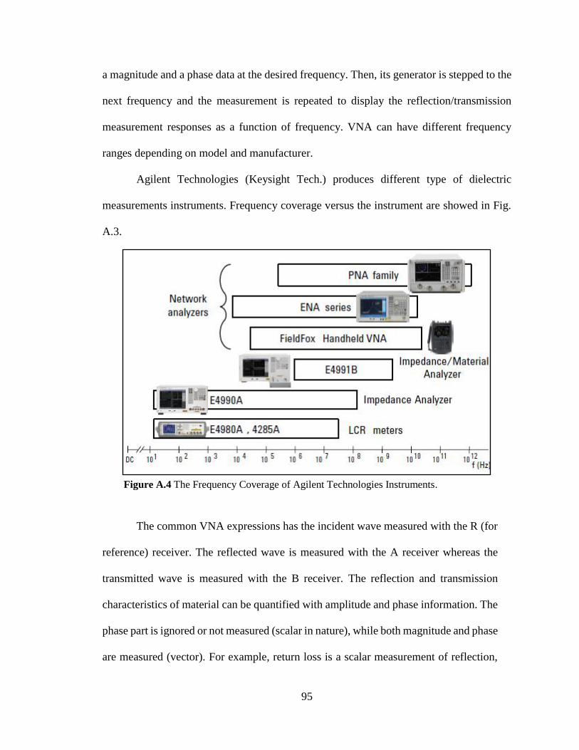
95
a magnitude and a phase data at the desired frequency. Then, its generator is stepped to the
next frequency and the measurement is repeated to display the reflection/transmission
measurement responses as a function of frequency. VNA can have different frequency
ranges depending on model and manufacturer.
Agilent Technologies (Keysight Tech.) produces different type of dielectric
measurements instruments. Frequency coverage versus the instrument are showed in Fig.
A.3.
The common VNA expressions has the incident wave measured with the R (for
reference) receiver. The reflected wave is measured with the A receiver whereas the
transmitted wave is measured with the B receiver. The reflection and transmission
characteristics of material can be quantified with amplitude and phase information. The
phase part is ignored or not measured (scalar in nature), while both magnitude and phase
are measured (vector). For example, return loss is a scalar measurement of reflection,
Figure A.4 The Frequency Coverage of Agilent Technologies Instruments.

96
while impedance results from a vector reflection measurement. Proportional reflection
is often displayed as A/R and proportional transmission is often shown as B/R, relating
to the measurement receivers used in the vector network analyzer (Fig. A.5).
6.2.2 Software (Agilent 85071E)
The measured data from the VNA is not presented in the convenient format for
microwave absorption properties. Therefore, software is required to convert the
measured data of scattering parameters to permittivity and permeability. The Agilent
Technologies 85071E materials measurement software determines the intrinsic
electromagnetic properties of dielectric and magnetic materials. The measurement is
based on the material` response to microwave energy. The divided screen and indicators
assistance in data analysis. Results can be generated in variety formats of
electromagnetic constitutive parameters and loss tangents values.
Figure A.5 The Network Analyzer Terminology with the parameters of reflection and
transmission.
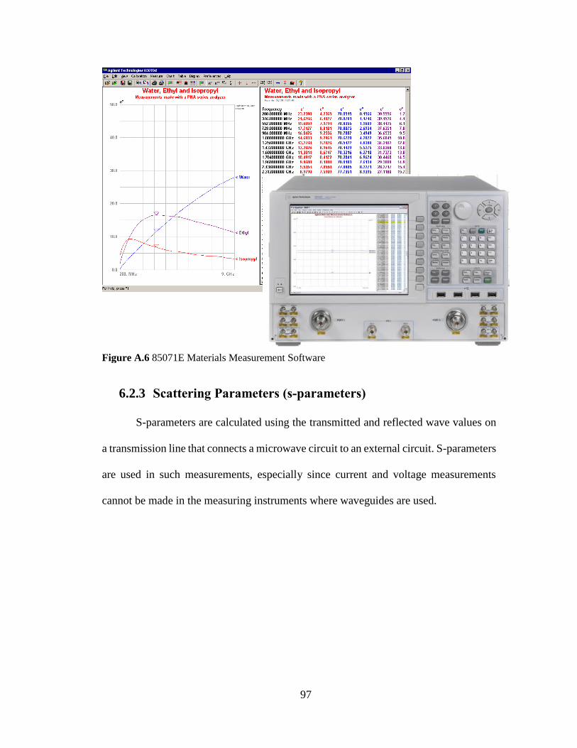
97
6.2.3 Scattering Parameters (s-parameters)
S-parameters are calculated using the transmitted and reflected wave values on
a transmission line that connects a microwave circuit to an external circuit. S-parameters
are used in such measurements, especially since current and voltage measurements
cannot be made in the measuring instruments where waveguides are used.
Figure A.6 85071E Materials Measurement Software

98
S-parameters can be calculated from the voltage values of the waves at the
connection points once a two port linear circuit is placed in a transmission line as shown
in Fig. A.7. The reflected and transmitted signals occur contrary to the stimulus signal
from the source. The voltage values of the reflected and transmitted signal are calculated
as follows:
111 VVV 222 VVV (A.8)
The current values (Eq. A.9) at these connection points are obtained from
voltage values using the characteristic impedance (Z0) of the transmission line:
)(
111
0
1
VVZ
I
)(1
22
0
2
VVZ
I
(A.9)
where the impedance is typically 50 ohm in microwave circuits. The voltages values of
transmitted and reflected wave can be substituted with Eq. A.8 and A.9 as Eq. A.10.
Figure A.7 A two-port network with “a” and “b” defined.
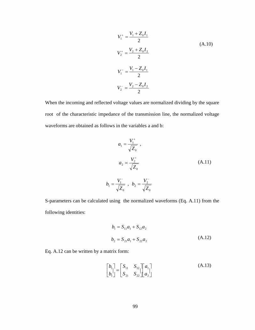
99
2
101
1
IZVV
2
202
2
IZVV
2
101
1
IZVV
2
202
2
IZVV
(A.10)
When the incoming and reflected voltage values are normalized dividing by the square
root of the characteristic impedance of the transmission line, the normalized voltage
waveforms are obtained as follows in the variables a and b:
0
11
Z
Va
,
0
22
Z
Va
0
11
Z
Vb
,
0
22
Z
Vb
(A.11)
S-parameters can be calculated using the normalized waveforms (Eq. A.11) from the
following identities:
2121111 aSaSb
2221212 aSaSb
(A.12)
Eq. A.12 can be written by a matrix form:
2
1
2221
1211
1
1
a
a
SS
SS
b
b
(A.13)

100
S-parameters are obtained for a two-port network given in Fig. A.7. If the reference
plane where placed the transmission line and the characteristic impedance of the
transmission line are known, the network can be fully characterized by the Eq. A.13.
In the network (Fig. A.7), the applied signal is fully consumed when an
impedance of transmission line is equal to the Z1 at port 2. Since there is no reflected
signal a2=0. Depending on that condition, the Eq. A.12 can be recalculated, then, S11
and S21 can be formatted as follows:
02 a için;
1
111
a
bS ,
1
221
a
bS
(A.14)
The applied signal is fully consumed when an impedance of transmission line is
equal to the Z1 at port 1. Since there is no reflected signal a1=0. Depending on that
condition, the Eq. A.12 can be recalculated, then, S11 and S21 can be formatted as
follows:
01 a için;
2
222
a
bS ,
2
112
a
bS
(A.15)
Figure A.8 A two-port network ended up a load.

101
6.2.4 Measurement Techniques
There are several measurement techniques to measure dielectric and magnetic
properties of materials. Researchers need to know which technique is more appropriate
for their materials.
Coaxial Probe
It is the best technique for the liquids and semi-solid (powder) materials. This
technique is simple, convenient, non-destructive and with one measurement. The
measurement system consists of a VNA or impedance analyzer, a coaxial probe and
software. The acceptable frequency range of this technique is between 10 MHz and 50
GHz.
Transmission Line
It is a broadband technique for machine-able solids. It puts the material inside a
portion of an enclosed transmission line. εr and µr are calculated from the measurement
of the reflected signal (S11) and transmitted signal (S21). Materials assumptions can be
listed as (i) Sample fills fixture cross section, (ii) No air gaps at fixture walls, (iii)
Smooth, flat faces, perpendicular to long axis, (iv) homogeneous.
Figure A.9 Transmission Line Method; waveguide and coaxial line scenario

102
Coaxial transmission line cover a broad frequency range, but a toroidal-shape
sample is more difficult to manufacture. A typical measurement system using transmission
line method consists of a VNA, a coaxial or waveguide transmission line and software to
calculate permittivity and permeability.
Figure A.10 Waveguide Measurement Setup (from lab)
Sample Holder Transmission Line
(a) (b)
(c)
MWCNTs
MnFe2O4
Powders
The Molded Sample
The Sample Holder
The Sample Rings
Figure A.11 Coaxial Line Measurement Setup (from lab)

103
Free-Space
Material assumptions are large scale, flat, parallel-faced samples. The technique
features are non-contacting, non-destructive, high frequency-low end limited by practical
sample size, useful for high temperature measurements, and measures magnetic materials.
Free-Space techniques use antennas to focus microwave energy at the material. It has
two typical setups: (i) S-parameter free space transmission configuration (ii) an NRL
arch reflectivity configuration. A typical system consists of a VNA, convenient free
space transmission reflectivity with the arch method, software.
The manufactured NRL arch system is shown in Fig. A.13. It is geometrically
designed depending on far field or near field conditions using different type of semi-
circular cast polyamide material, which is one of the materials involved in polyamide
group. It is manufactured by casting; it has a tight structure and hardness and low
reflection values against to microwaves. Therefore, it is preferred to use for the arch
system to make less reflection from the measurement environment.
Figure A.12 Free-Space Measurement Setups

104
The other measurement techniques (Resonant Cavity, Parallel Plate, and
Inductance measurement) are summarized in Fig. A.14.
Figure A.13 Free-Space Measurement Setups (from lab)

105
Figure A.14 A Summary of Measurement Techniques.
106
Bibliography
[1] G. Rao, S. Mahulikar, Integrated review of stealth technology and its role in airpower, The
aeronautical journal. 106 (2002) 629-642.
[2] A. Teber, K. Cil, T. Yilmaz, B. Eraslan, D. Uysal, G. Surucu, A.H. Baykal, R. Bansal, Manganese
and Zinc Spinel Ferrites Blended with Multi-Walled Carbon Nanotubes as Microwave Absorbing
Materials, Aerospace. 4 (2017) 2.
[3] I. Specialty Materials, Manufacturers of Boron and SCS Silicon Carbide Fibers and Boron
Nanopowder.
[4] L. Chen, C. Ong, C. Neo, V. Varadan, V.K. Varadan, Microwave electronics: measurement and
materials characterization, John Wiley & Sons, 2004.
[5] P. Liu, Y. Huang, J. Yan, Y. Yang, Y. Zhao, Construction of CuS nanoflakes vertically aligned on
magnetically decorated graphene and their enhanced microwave absorption properties, ACS
applied materials & interfaces. 8 (2016) 5536-5546.
[6] Z. Wang, L. Wu, J. Zhou, W. Cai, B. Shen, Z. Jiang, Magnetite nanocrystals on multiwalled carbon
nanotubes as a synergistic microwave absorber, The Journal of Physical Chemistry C. 117 (2013)
5446-5452.
[7] T. Giannakopoulou, L. Kompotiatis, A. Kontogeorgakos, G. Kordas, Microwave behavior of ferrites
prepared via sol–gel method, J Magn Magn Mater. 246 (2002) 360-365.
[8] A. Jänis, R.T. Olsson, S. Savage, U.W. Gedde, U. Klement, Microwave absorbing properties of
ferrite-based nanocomposites. 6526 (2007) 65261P.
[9] O. Akman, H. Kavas, A. Baykal, M.S. Toprak, A. Çoruh, B. Aktaş, Magnetic metal nanoparticles
coated polyacrylonitrile textiles as microwave absorber, J Magn Magn Mater. 327 (2013) 151-158.
[10] L. Solymar, D. Walsh, Electrical properties of materials, OUP Oxford, 2009.
[11] W. Zachariasen, C. Kittel, Introduction to solid state physics (1966).
[12] A. Von Hippel, Dielectrics and Waves , Artech House, Inc., Norwood, MA (1995).

107
[13] S. Nelson, Dielectric properties measurement techniques and applications, Trans. ASAE. 42
(1999) 523.
[14] D.C. Jiles, Introduction to the electronic properties of materials, CRC Press, 2001.
[15] P. Robert, Electrical and magnetic properties of materials, Artech House Publishers, 1988.
[16] D. Jiles, Recent advances and future directions in magnetic materials, Acta Materialia. 51 (2003)
5907-5939.
[17] M. Tinkham, Introduction to superconductivity, Courier Corporation, 1996.
[18] M.E. Lines, A.M. Glass, Principles and applications of ferroelectrics and related materials, Oxford
university press, 1977.
[19] M.I. Montrose, EMC and the printed circuit board: design, theory, and layout made simple, John
Wiley & Sons, 2004.
[20] S. Ramo, J.R. Whinnery, T. Van Duzer, Fields and waves in communication electronics, John
Wiley & Sons, 2008.
[21] C.A. Balanis, Advanced engineering electromagnetics, John Wiley & Sons, 1999.
[22] Agilent, Basics of Measuring the Dielectric Properties of Materials Application Note.
[23] E. Nyfors, P. Vainikainen, Industrial microwave sensors, Artech House Publishers, 1989.
[24] C. Brosseau, J.B. Youssef, P. Talbot, A. Konn, Electromagnetic and magnetic properties of
multicomponent metal oxides heterostructures: Nanometer versus micrometer-sized particles, J.
Appl. Phys. 93 (2003) 9243-9256.
[25] Y. Yin, M. Zeng, J. Liu, W. Tang, H. Dong, R. Xia, R. Yu, Enhanced high-frequency absorption
of anisotropic Fe3O4/graphene nanocomposites, Scientific reports. 6 (2016) 25075.
[26] V. Bogush, Application of electroless metal deposition for advanced composite shielding
materials, Journal of Optoelectronics and Advanced Materials. 7 (2005) 1635-1642.
[27] R.J.W. Donald, and M. Mardiguian, A Handbook Series on Electromagnetic Interference and
Compatibility: Electromagnetic Shielding, Interference Control Technologies, ISBN-13:978-
0944916032 . (1988).

108
[28] J.I. Duffy, M.W. Ranney, Electroless and other nonelectrolytic plating techni ques: recent
developments, Noyes Data Corp., 1980.
[29] D. Tsai, S. Kim, T. Corrigan, R.J. Phaneuf, M.R. Zachariah, Electrostatic-directed deposition of
nanoparticles on a field generating substrate, Nanotechnology. 16 (2005) 1856.
[30] V. Bogush, V. Glybin, L. Lynkov, Synthesis of inorganic nanoparticles in fiber polymers and their
properties, Physics, Chemistry and Application of Nanostructures (1999) 251-254.
[31] A.V. Pandya, Study of the comparison of Conducting Behavior of doped Macromolecules and
Semiconductors, Imperial Journal of Interdisciplinary Research. 2 (2016).
[32] L. Lynkov, V. Glybin, T. Selivyorstova, and V. Bogush, A method for ion-exchanging fibre
material production. (2003).
[33] F.A. Lowenheim, Electroplating--Fundamentals of Surface Finishing, McGraw-Hill Book Co.,
New York.1978, 560 (1978).
[34] Y. Naito, K. Suetake, Application of ferrite to electromagnetic wave absorber and its
characteristics, IEEE Trans. Microwave Theory Tech. 19 (1971) 65-72.
[35] N. Bensebaa, N. Loudjani, S. Alleg, L. Dekhil, J. Suñol, M. Al Sae, M. Bououdina, XRD analysis
and magnetic properties of nanocrystalline Ni 20 Co 80 alloys, J Magn Magn Mater. 349 (2014)
51-56.
[36] A. Taylor, R.W. Floyd, Precision measurements of lattice parameters of non-cubic crystals, Acta
Crystallogr. 3 (1950) 285-289.
[37] B. Cullity, Elements of X-ray Diffraction. Addison and Wesley Publishing Company Inc, Reading,
USA (1978) 32-106.
[38] E. Jeon, Y. Cho, Mechanochemical synthesis and thermal decomposition of zinc borohydride, J.
Alloys Compounds. 422 (2006) 273-275.
[39] M. Spasojević, L. Ribić-Zelenović, A. Maričić, The phase structure and morphology of
electrodeposited nickel-cobalt alloy powders, Science of Sintering. 43 (2011) 313-326.

109
[40] L.D. Rafailović, D.M. Minić, Deposition and characterisation of nanostructured nickel–cobalt
alloys, Hem.ind. 63 (2009) 557-569.
[41] R.W.G. Wyckoff, R.W. Wyckoff, Crystal structures, Interscience New York, 1960.
[42] Y. Li, L. Li, H. Liao, H. Wang, Preparation of pure nickel, cobalt, nickel–cobalt and nickel–copper
alloys by hydrothermal reduction, Journal of Materials Chemistry. 9 (1999) 2675-2677.
[43] W.B. Weir, Automatic measurement of complex dielectric constant and permeability at microwave
frequencies, Proc IEEE. 62 (1974) 33-36.
[44] A. Aslam, M. Islam, I. Ali, M. Awan, M. Irfan, A. Iftikhar, High frequency electrical transport
properties of CoFe 2 O 4 and Sr 2 NiMnFe 12 O 22 composite ferrites, Ceram. Int. 40 (2014) 155-
162.
[45] X. Liu, B. Li, D. Geng, W. Cui, F. Yang, Z. Xie, D. Kang, Z. Zhang, (Fe, Ni)/C nanocapsules for
electromagnetic-wave-absorber in the whole Ku-band, Carbon. 47 (2009) 470-474.
[46] Z. Xie, D. Geng, X. Liu, S. Ma, Z. Zhang, Magnetic and microwave-absorption properties of
graphite-coated (Fe, Ni) nanocapsules, Journal of Materials Science & Technology. 27 (2011) 607-
614.
[47] X. Liu, Z. Ou, D. Geng, Z. Han, H. Wang, B. Li, E. Brück, Z. Zhang, Enhanced absorption
bandwidth in carbon-coated supermalloy FeNiMo nanocapsules for a thin absorb thickness, J.
Alloys Compounds. 506 (2010) 826-830.
[48] O. Akman, H. Kavas, A. Baykal, M.S. Toprak, A. Çoruh, B. Aktaş, Magnetic metal nanoparticles
coated polyacrylonitrile textiles as microwave absorber, J Magn Magn Mater. 327 (2013) 151-158.
[49] H. Lin, H. Zhu, H. Guo, L. Yu, Investigation of the microwave-absorbing properties of Fe-filled
carbon nanotubes, Mater Lett. 61 (2007) 3547-3550.
[50] T. Zou, H. Li, N. Zhao, C. Shi, Electromagnetic and microwave absorbing properties of multi-
walled carbon nanotubes filled with Ni nanowire, J. Alloys Compounds. 496 (2010) L22-L24.
[51] Y. Qing, W. Zhou, F. Luo, D. Zhu, Epoxy-silicone filled with multi-walled carbon nanotubes and
carbonyl iron particles as a microwave absorber, Carbon. 48 (2010) 4074-4080.

110
[52] J. Qiu, T. Qiu, Fabrication and microwave absorption properties of magnetite nanoparticle–carbon
nanotube–hollow carbon fiber composites, Carbon. 81 (2015) 20-28.
[53] D. Zhang, F. Xu, J. Lin, Z. Yang, M. Zhang, Electromagnetic characteristics and microwave
absorption properties of carbon-encapsulated cobalt nanoparticles in 2–18-GHz frequency range,
Carbon. 80 (2014) 103-111.
[54] H. Lin, H. Zhu, H. Guo, L. Yu, Microwave-absorbing properties of Co-filled carbon nanotubes,
Mater. Res. Bull. 43 (2008) 2697-2702.
[55] D. Shi, P. He, P. Zhao, F.F. Guo, F. Wang, C. Huth, X. Chaud, S.L. Bud’ko, J. Lian, Magnetic
alignment of Ni/Co-coated carbon nanotubes in polystyrene composites, Composites Part B:
Engineering. 42 (2011) 1532-1538.
[56] G. Liu, L. Wang, G. Chen, S. Hua, C. Ge, H. Zhang, R. Wu, Enhanced electromagnetic absorption
properties of carbon nanotubes and zinc oxide whisker microwave absorber, J. Alloys Compounds.
514 (2012) 183-188.
[57] K.R. Paton, A.H. Windle, Efficient microwave energy absorption by carbon nanotubes, Carbon.
46 (2008) 1935-1941.
[58] M. Lu, W. Cao, H. Shi, X. Fang, J. Yang, Z. Hou, H. Jin, W. Wang, J. Yuan, M. Cao, Multi-wall
carbon nanotubes decorated with ZnO nanocrystals: mild solution-process synthesis and highly
efficient microwave absorption properties at elevated temperature, Journal of Materials Chemistry
A. 2 (2014) 10540-10547.
[59] A. Teber, I. Unver, H. Kavas, B. Aktas, R. Bansal, Knitted radar absorbing materials (RAM) based
on nickel–cobalt magnetic materials, J Magn Magn Mater. 406 (2016) 228-232.
[60] K. Khan, Microwave absorption properties of radar absorbing nanosized cobalt ferrites for high
frequency applications, Journal of Superconductivity and Novel Magnetism. 27 (2014) 453-461.
[61] V. Sunny, P. Kurian, P. Mohanan, P. Joy, M. Anantharaman, A flexible microwave absorber based
on nickel ferrite nanocomposite, J. Alloys Compounds. 489 (2010) 297-303.

111
[62] J. Xie, M. Han, L. Chen, R. Kuang, L. Deng, Microwave-absorbing properties of NiCoZn spinel
ferrites, J Magn Magn Mater. 314 (2007) 37-42.
[63] D. Zhao, Q. Lv, Z. Shen, Fabrication and microwave absorbing properties of Ni–Zn spinel ferrites,
J. Alloys Compounds. 480 (2009) 634-638.
[64] A.M. Gama, M.C. Rezende, C.C. Dantas, Dependence of microwave absorption properties on
ferrite volume fraction in MnZn ferrite/rubber radar absorbing materials, J Magn Magn Mater. 323
(2011) 2782-2785.
[65] S.H. Hosseini, A. Asadnia, Synthesis, characterization, and microwave-absorbing properties of
polypyrrole/MnFe 2 O 4 nanocomposite, Journal of Nanomaterials. 2012 (2012) 3.
[66] R. Sui, P. Charpentier, Synthesis of metal oxide nanostructures by direct sol–gel chemistry in
supercritical fluids, Chem. Rev. 112 (2012) 3057-3082.
[67] L. Chen, C. Ong, C. Neo, V. Varadan, V.K. Varadan, Microwave electronics: measurement and
materials characterization, John Wiley & Sons, 2004.
[68] I. U.S. Research Nanomaterials, The Advanced Nanomaterials Provider.
[69] D.P. Debecker, V. Hulea, P.H. Mutin, Mesoporous mixed oxide catalysts via non-hydrolytic sol–
gel: a review, Applied Catalysis A: General. 451 (2013) 192-206.
[70] J. Feng, H. Zhang, Hybrid materials based on lanthanide organic complexes: a review, Chem. Soc.
Rev. 42 (2013) 387-410.
[71] A. Demir, S. Güner, Y. Bakis, S. Esir, A. Baykal, Magnetic and optical properties of Mn1−
xZnxFe2O4 nanoparticles, Journal of Inorganic and Organometallic Polymers and Materials. 24
(2014) 729-736.
[72] Agilent Literature, Agilent Basics of Measuring the Dielectric Properties of Materials, Application
Note. .
[73] D. Micheli, R. Pastore, G. Giannini, A. Vricella, M. Marchetti,
Low-cost low-observable satellites made of carbon nanostructured multilayers: Numerical
investigation of scattering. (2013).
112
[74] D. Micheli, C. Apollo, R. Pastore, R.B. Morles, M. Marchetti, G. Gradoni, Electromagnetic
characterization of composite materials and microwave absorbing modeling, in: Advances in
nanocomposites-synthesis, characterization and industrial applications, InTech, 2011.
[75] D. Micheli, C. Apollo, R. Pastore, R.B. Morles, S. Laurenzi, M. Marchetti, Nanostructured
composite materials for electromagnetic interference shielding applications, Acta Astronaut. 69
(2011) 747-757.
[76] G. Fang, Z. Chen, H. Li, Synthesis and properties of microencapsulated paraffin composites with
SiO 2 shell as thermal energy storage materials, Chem. Eng. J. 163 (2010) 154-159.
[77] F. Gözüak, Y. Köseoğlu, A. Baykal, H. Kavas, Synthesis and characterization of CoxZn 1− xFe 2
O 4 magnetic nanoparticles via a PEG-assisted route, J Magn Magn Mater. 321 (2009) 2170-2177.
[78] K. Kanade, D. Amalnerkar, H. Potdar, B. Kale, Nanocrystalline Mn–Zn–ferrite by novel oxalato-
hydrazinated complex method, Mater. Chem. Phys. 117 (2009) 187-191.
[79] S. Apte, S. Naik, R. Sonawane, B. Kale, J. Baeg, Synthesis of Nanosize‐Necked Structure α‐and
γ‐Fe2O3 and its Photocatalytic Activity, J Am Ceram Soc. 90 (2007) 412-414.
[80] G. Brahmachari, S. Laskar, P. Barik, Magnetically separable MnFe 2 O 4 nano-material: an
efficient and reusable heterogeneous catalyst for the synthesis of 2-substituted benzimidazoles and
the extended synthesis of quinoxalines at room temperature under aerobic conditions, RSC
Advances. 3 (2013) 14245-14253.
[81] Z. Tang, C. Sorensen, K. Klabunde, G. Hadjipanayis, Size-dependent Curie temperature in
nanoscale MnFe 2 O 4 particles, Phys. Rev. Lett. 67 (1991) 3602.
[82] T.M. Clark, B. Evans, Enhanced magnetization and cation distributions in nanocrystalline
ZnFe/sub 2/O/sub 4: a conversion electron Mossbauer spectroscopic investigation, IEEE Trans.
Magn. 33 (1997) 3745-3747.
[83] A. Jänis, R.T. Olsson, S. Savage, U.W. Gedde, U. Klement, Microwave absorbing properties of
ferrite-based nanocomposites. 6526 (2007) 65261P.

113
[84] S.H. Ahmad, M.H. Abdullah, D. Hui, A.N. Yusoff, D. Puryanti, Magnetic and microwave
absorbing properties of magnetite–thermoplastic natural rubber nanocomposites, J Magn Magn
Mater. 322 (2010) 3401-3409.
[85] Y. Yin, M. Zeng, J. Liu, W. Tang, H. Dong, R. Xia, R. Yu, Enhanced high-frequency absorption
of anisotropic Fe3O4/graphene nanocomposites, Scientific reports. 6 (2016) 25075.
[86] H. Zhao, Z. Fu, H. Chen, M. Zhong, C. Wang, Excellent electromagnetic absorption capability of
Ni/carbon based conductive and magnetic foams synthesized via a green one pot route, ACS
applied materials & interfaces. 8 (2016) 1468-1477.
[87] J. Xiang, J. Li, X. Zhang, Q. Ye, J. Xu, X. Shen, Magnetic carbon nanofibers containing uniformly
dispersed Fe/Co/Ni nanoparticles as stable and high-performance electromagnetic wave absorbers,
Journal of Materials Chemistry A. 2 (2014) 16905-16914.
[88] X. Liu, Z. Ou, D. Geng, Z. Han, J. Jiang, W. Liu, Z. Zhang, Influence of a graphite shell on the
thermal and electromagnetic characteristics of FeNi nanoparticles, Carbon. 48 (2010) 891-897.
[89] H. Sözeri, Z. Mehmedi, H. Kavas, A. Baykal, Magnetic and microwave properties of BaFe 12 O
19 substituted with magnetic, non-magnetic and dielectric ions, Ceram. Int. 41 (2015) 9602-9609.
[90] Y. Naito, K. Suetake, Application of ferrite to electromagnetic wave absorber and its
characteristics, IEEE Trans. Microwave Theory Tech. 19 (1971) 65-72.
[91] Z. Wang, L. Wu, J. Zhou, W. Cai, B. Shen, Z. Jiang, Magnetite nanocrystals on multiwalled carbon
nanotubes as a synergistic microwave absorber, The Journal of Physical Chemistry C. 117 (2013)
5446-5452.
[92] T. Giannakopoulou, L. Kompotiatis, A. Kontogeorgakos, G. Kordas, Microwave behavior of
ferrites prepared via sol–gel method, J Magn Magn Mater. 246 (2002) 360-365.
[93] Sotirios K. Goudos (Ed.), Microwave Systems and Applications, InTech, Chapters published
January 11, 2017 under CC BY 3.0 license, 2017.
[94] A. Öztürk, R. Süleymanli, B. Aktaş, A. Teber, Propagation of microwaves in periodic layered
media (2010) 4-7.

114
[95] A. Ozturk, R. Suleymanli, B. Aktas, A. Teber, Effect of Thin Metallic Layers on the Refractive
Index of a Multilayer System, Chinese Physics Letters. 29 (2012) 027301.
[96] S. Abbas, A. Dixit, R. Chatterjee, T. Goel, Complex permittivity, complex permeability and
microwave absorption properties of ferrite–polymer composites, J Magn Magn Mater. 309 (2007)
20-24.
[97] P. Liu, Y. Huang, J. Yan, Y. Yang, Y. Zhao, Construction of CuS nanoflakes vertically aligned on
magnetically decorated graphene and their enhanced microwave absorption properties, ACS
applied materials & interfaces. 8 (2016) 5536-5546.
[98] M. Wu, Y. Zhang, S. Hui, T. Xiao, S. Ge, W. Hines, J. Budnick, G. Taylor, Microwave magnetic
properties of Co 50/(SiO 2) 50 nanoparticles, Appl. Phys. Lett. 80 (2002) 4404-4406.
[99] J. Luo, P. Shen, W. Yao, C. Jiang, J. Xu, Synthesis, characterization, and microwave absorption
properties of reduced graphene oxide/strontium ferrite/polyaniline nanocomposites, Nanoscale
research letters, 11 no:1 (2016) 141.