Development of Quantum Dot Solar Cells - New test sitembe.rcast.u-tokyo.ac.jp/pdf/QD solar...
14
Development of Quantum Dot Solar Cells Okada Laboratory Research Center for Advanced Science & Technology The University of Tokyo
-
Upload
truonghanh -
Category
Documents
-
view
213 -
download
1
Transcript of Development of Quantum Dot Solar Cells - New test sitembe.rcast.u-tokyo.ac.jp/pdf/QD solar...

Development of Quantum Dot Solar Cells
Okada Laboratory
Research Center for Advanced Science & TechnologyThe University of Tokyo

AM1.5
Wavelength
Efficient absorption by using multiple bandgaps
AM1.5
Wavelength
Efficient absorption by using multiple bandgaps
Efficient use of high-energysolar radiation
AM1.5
Wavelength
Efficient use of high-energysolar radiation
AM1.5
Wavelength
Hot carriers
3 V
Multiple junctions(Quantum size effect)
Eg
Intermediate bands(QD superlattice)
Multiple excitongeneration (MEG)
3 I
nanoscaleformats
Innovative PV : 50% Efficient Solar Cells

Intermediate Band Solar Cell:Principle
A. Luque and A. Martí, Phys. Rev. Lett. 78, 5014 (1997)
Conduction Band
Intermediate Band (IB)
p –type Host Semiconductor
n-type HostSemiconductor
IB 材料
Valence Band

Intermediate Band Solar Cell:Theoretical Efficiencies
η = 47% (1sun)η = 63% (Maximum concentration)
Maximum concentration1sun
5010Efficiency (%)
47%Eg=2.4 eVECI=0.9 eV
45
40
20
35
3025
15
1.5 2 2.5 30
0.5
1
E IV
(eV)
Eg (eV)
CB
-IB e
nerg
y ga
p(e
V)
CB-VB energy gap (eV)
Efficiency (%)
63%Eg=1.9 eVECI=0.7 eV
30
60
7010
5040
20
1.5 2 2.5 30
0.5
1
EIV
(eV)
Eg (eV)
CB
-IB e
nerg
y ga
p(e
V)
CB-VB energy gap (eV)
Y. Okada et al, Oyo-Buturi, 79, 206 (2010)

Intermediate Band Realized with 3D Quantum dot Superlattice
VB
CB
miniband
InAs QDGaAs
VB
CB
InAs QD
GaAs GaAs
GaAs
InAs QD
Single QDSingle QD 3D QD Superlattice3D QD Superlattice

Frank-van der Merwe Volmer-Weber Stranski-Krastanov (S-K)
2D Growth 3D Growth 2D→3D
Self-Assembled Growth of Quantum Dots
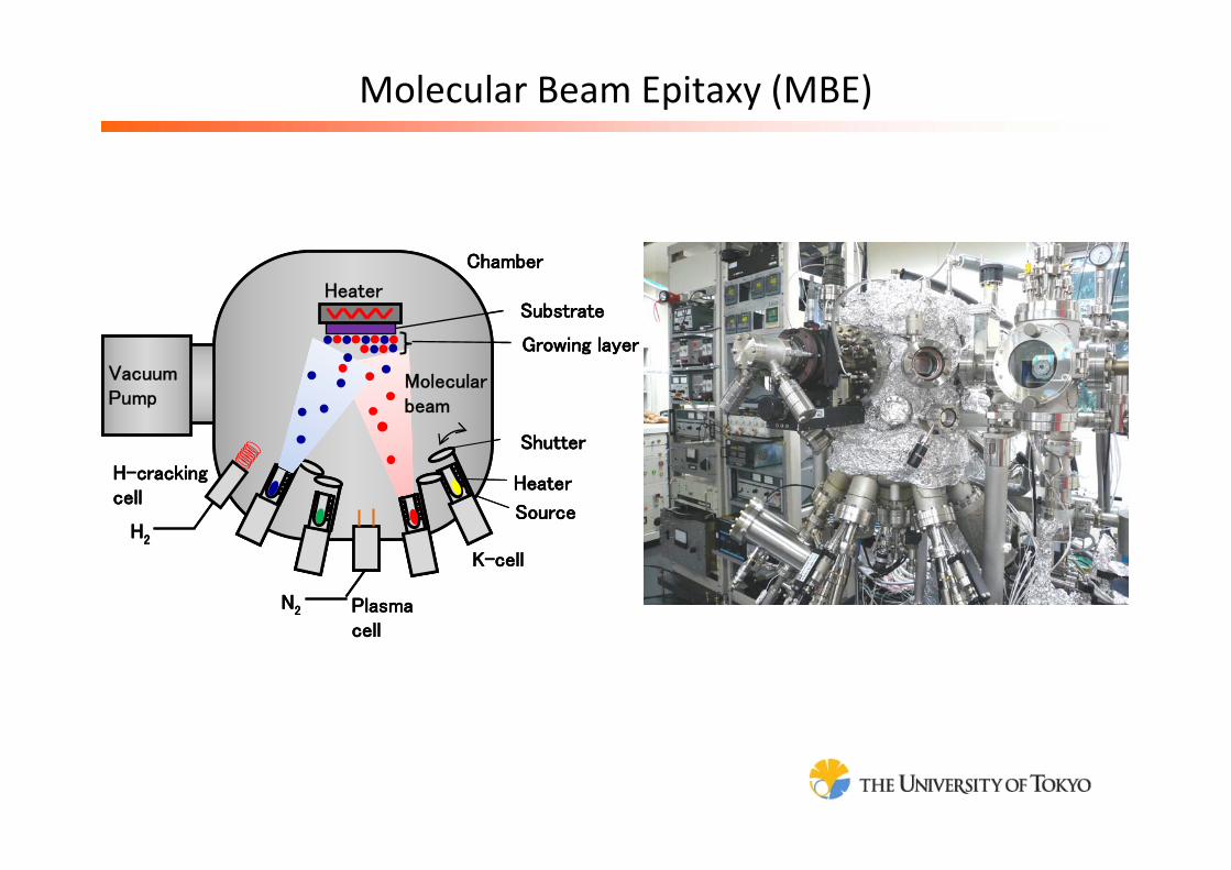
Molecular Beam Epitaxy (MBE)
Substrate
Source
Shutter
Heater
Growing layer
Chamber
VacuumPump
Heater
K-cell
Molecular beam
N2
H2
Plasma cell
H-cracking cell
Substrate
Source
Shutter
Heater
Growing layer
Chamber
VacuumPump
Heater
K-cell
Molecular beam
N2
H2
Plasma cell
H-cracking cell

InGaAs on (311)BInAs on (100)
K. Akahane et al, APL 73 (1998) 3411
Self-Organized InGaAs Quantum Dots on (311)B Substrate
QDs on (311)B substrate show;(1) Better size homogeneity(2) Higher in-plane density(3) Ordered periodic structure(4) Better heterointerface quality

Z.R. Wasilewski et al. JCG 201 (1999) 1131
Fabrication of 3D Quantum Dot Superlattice: Strain-Balancing
Accumulation of lattice strainin conventional approach
Strain-compensation growth: Strain/layer is balanced out
QDSpacer
Strainfield

InGaAlAs
III-V multijunction solar cells
GaAsP
Strain-Compensation Materials

Self-Organized Stacked InAs QDs on InP(311)B Substrates
Spacer thickness d = 20 nmNumber of stacked QDs = 30 layers
Average diameter = 63.2nmIn-plane dot density = 2.7×1010cm-2
Size uniformity ~ 12.3% Y. Okada et al, EU-PVSEC, Barcelona (2005)

on GaAs (311)B
InGaAs/GaNAs Quantum Dot Solar Cell : 1sun
ISC(mA/cm2)
VOC(V)
FF Efficiency(%)
QD solar cell on GaAs(311)B 24.26 0.791 0.840 16.12
Y. Okada, MRS Fall Meeting (Boston, 2008)

IB (3D QD Superlattice) Solar Cell:On-going Developments
A. Luque et al. Journal of Applied Physics 96, 903 (2004)
InAs/GaAs
IES-UPMUniv. of Glasgow
S. M. Hubbard et al. Applied Physics Letters 92, 123512 (2008)
Rochester Institute of TechnologyNASA
InAs/GaAsP InAs/Ga(N)As/GaAs
Univ. of Tokyo
Y. Okada et al. Journal of Applied Physics 106, 024306 (2009)
V. Popescu et al. Phys. Rev. B 78, 205321 (2008)
InAs/GaAsP InAs/AlGaAs
S. A. Blokhin et al. Physics of semiconductor Devices 43, 514 (2009)
St. Petersburg Russian AcademyIoffe Institute
NREL
η = 15.7% (100)16.1% (311)B
η = 18.32%

Intermediate Band (Quantum Dot Superlattice) Solar Cell
・ Efficiencies > 60% (under concentration) are possible with intermediate band solar cells. Concentrator cells are very cost-effective.
・ Fabrication of high-quality 3D quantum dot superlattice is required asa good intermediate band.
・Good size uniformity (< 10%) ・High density resulting in higher absorption・Close packing resulting in miniband formation
(dot spacing < 10nm)・Optimization of bandgap energies of materials
・ Top-down approaches are attractive for reducing cost.・ Photon management helps increase optical absorption in IB.
This work is supported by NEDO and METI, Japan.
Should be achieved soon