Development of Automated Production Line Processes for Solar ...
101
A national laboratory of the U.S. Department of Energy Office of Energy Efficiency & Renewable Energy National Renewable Energy Laboratory Innovation for Our Energy Future Development of Automated Production Line Processes for Solar Brightfield Modules Final Report 1 June 2003 – 30 November 2007 M. Nowlan Spire Corporation Bedford, Massachusetts Subcontract Report NREL/SR-520-43190 April 2008 NREL is operated by Midwest Research Institute ● Battelle Contract No. DE-AC36-99-GO10337
Transcript of Development of Automated Production Line Processes for Solar ...

A national laboratory of the U.S. Department of EnergyOffice of Energy Efficiency & Renewable Energy
National Renewable Energy Laboratory Innovation for Our Energy Future
Development of Automated Production Line Processes for Solar Brightfield Modules Final Report 1 June 2003 – 30 November 2007 M. Nowlan Spire Corporation Bedford, Massachusetts
Subcontract Report NREL/SR-520-43190 April 2008
NREL is operated by Midwest Research Institute ● Battelle Contract No. DE-AC36-99-GO10337
National Renewable Energy Laboratory1617 Cole Boulevard, Golden, Colorado 80401-3393 303-275-3000 • www.nrel.gov
Operated for the U.S. Department of Energy Office of Energy Efficiency and Renewable Energy by Midwest Research Institute • Battelle
Contract No. DE-AC36-99-GO10337
Subcontract Report NREL/SR-520-43190 April 2008
Development of Automated Production Line Processes for Solar Brightfield Modules Final Report 1 June 2003 – 30 November 2007 M. Nowlan Spire Corporation Bedford, Massachusetts
NREL Technical Monitor: Brian Keyes Prepared under Subcontract No. ZDO-2-30628-12

This publication was reproduced from the best available copy Submitted by the subcontractor and received no editorial review at NREL
NOTICE This report was prepared as an account of work sponsored by an agency of the United States government. Neither the United States government nor any agency thereof, nor any of their employees, makes any warranty, express or implied, or assumes any legal liability or responsibility for the accuracy, completeness, or usefulness of any information, apparatus, product, or process disclosed, or represents that its use would not infringe privately owned rights. Reference herein to any specific commercial product, process, or service by trade name, trademark, manufacturer, or otherwise does not necessarily constitute or imply its endorsement, recommendation, or favoring by the United States government or any agency thereof. The views and opinions of authors expressed herein do not necessarily state or reflect those of the United States government or any agency thereof.
Available electronically at http://www.osti.gov/bridge
Available for a processing fee to U.S. Department of Energy and its contractors, in paper, from:
U.S. Department of Energy Office of Scientific and Technical Information P.O. Box 62 Oak Ridge, TN 37831-0062 phone: 865.576.8401 fax: 865.576.5728 email: mailto:[email protected]
Available for sale to the public, in paper, from: U.S. Department of Commerce National Technical Information Service 5285 Port Royal Road Springfield, VA 22161 phone: 800.553.6847 fax: 703.605.6900 email: [email protected] online ordering: http://www.ntis.gov/ordering.htm
Printed on paper containing at least 50% wastepaper, including 20% postconsumer waste
TABLE OF CONTENTS
Page
1 INTRODUCTION ........................................................................................................................... 1 1.1 Objective............................................................................................................................. 1 1.2 Approach............................................................................................................................. 1 2 PHASE 1 TECHNICAL DISCUSSION.......................................................................................... 2 2.1 Task 1 – Design Brightfield Module and Production Line ................................................ 2 2.1.1 Brightfield Photovoltaic Module Design............................................................... 2 2.1.2 BOS Electrical Design Analysis............................................................................ 6 2.1.3 Production Line Definition.................................................................................... 8 2.2 Task 2 – Develop Cell String Inspection Process............................................................... 9 2.2.1 Visible Defect Inspections................................................................................... 10 2.2.2 Microcrack Inspection ........................................................................................ 12 2.2.3 String Inspection System Integration................................................................... 17 2.3 Task 3 – Develop Advanced Lamination Process ............................................................ 19 2.3.1 Fast Curing Encapsulant ...................................................................................... 19 2.3.2 Laminator Heater Thermal Compound................................................................ 21 2.4 Task 4 – Design Module Lay-up System.......................................................................... 22 2.4.1 Stacking on a Tray ............................................................................................... 22 2.4.2 Winding onto a Tube ........................................................................................... 24 2.4.3 Direct Dispensing onto the Module..................................................................... 24 2.5 Task 5 – Design String Busing System ............................................................................ 25 2.5.1 Bus Ribbon Fabrication ....................................................................................... 25 2.5.2 Bus Ribbon and Diode Installation – SCARA Robot Approach......................... 27 2.5.3 Bus Ribbon and Diode Installation – Cartesian Robot Approach....................... 28 2.5.4 Automated Soldering Process Development ....................................................... 32 3 PHASE 2 TECHNICAL DISCUSSION........................................................................................ 34 3.1 Task 6 – Fabricate and Test Module Lay-up System ....................................................... 34 3.2 Task 7 – Fabricate & Test String Busing System............................................................. 36 3.2.1 Bus Ribbon Fabrication ....................................................................................... 36 3.2.2 Bus Ribbon and Diode Installation...................................................................... 38 3.2.3 Development Work at ARRI ............................................................................... 40 3.3 Task 8 – Design Advanced Lamination Process Tool...................................................... 43 3.4 Task 9 – Design Lamination Automation......................................................................... 48 3.5 Task 10 – Design Large Area Solar Simulator ................................................................. 49 3.5.1 Single-Flash Long Pulse Xenon Light Source..................................................... 49 3.5.2 Large Area Optical Test Bed ............................................................................... 51 3.5.3 High Power Electronic Load ............................................................................... 52 3.6 Task 11 – Develop Soldering Process for Thin Cells....................................................... 53 4 PHASE 3 TECHNICAL DISCUSSION........................................................................................ 55 4.1 Task 14 – Fabricate and Test Large Area Simulator ........................................................ 55 4.1.1 Final Design, Fabrication, and Assembly of a Large Area Simulator................. 55 4.1.2 Large Area Simulator Testing ............................................................................. 62 4.2 Task 15 – Develop Computer Integrated System for Module Manufacturing ................. 67
iii
TABLE OF CONTENTS (CONCLUDED)
Page
4.2.1 SCADA Software Prototype................................................................................ 68 4.2.2 Scaling SCADA to a Full PV Module Production Line...................................... 72 4.3 Task 16 – Development of Low-stress Cell String Assembly Processes ......................... 77 4.3.1 New Machine Design .......................................................................................... 77 4.3.2 Back Contact Cells .............................................................................................. 80 4.3.3 Flux Application .................................................................................................. 81 4.3.4 Solar Cell Handling ............................................................................................. 82 4.3.5 Pre-heating Process for Cell Soldering................................................................ 85 4.3.6 Ribbon Corrugator ............................................................................................... 86 5 CONCLUSIONS................................................................................................................................. 87 6 REFERENCES ................................................................................................................................... 91
iv

LIST OF FIGURES
Page
1 PV sub-arrays at Tucson Electric Power in Springerville, AZ .............................................................. 2 2 Diode assembly temperature rise vs. forward current............................................................................ 3 3 Module circuit with laminated diodes and center outputs. .................................................................... 4 4 Module circuit with laminated by-pass diodes and end outputs. ........................................................... 4 5 Isometric CAD views of the Brightfield module design........................................................................ 5 6 Bending stress profile under maximum wind and snow load. ............................................................... 6 7 Module glass and steel deflection under 113 psf wind and snow load. ................................................. 6 8 Brightfield module line process flow chart. ........................................................................................... 8 9 Preliminary module production line floor plan for the large area Brightfield module. ......................... 9 10 Prototype automated cell string inspection system with a string of 125 mm cells. ............................... 9 11 Vision sensor images of a 125 mm polycrystalline silicon cell. .......................................................... 10 12 Cell front side vision sensor with a string of 125 mm cells. ................................................................ 11 13 Cell backside vision sensor, LED array, backlight, and mirror. .......................................................... 11 14 String front side vision inspection tools on a 125 mm polycrystalline Si cell..................................... 12 15 String back side vision inspection tools on a 125 mm polycrystalline Si cell. .................................... 12 16 IR images of a Si solar cell before and after the application of ultrasonic energy. ............................. 13 17 Cell flexer on test stand........................................................................................................................ 14 18 Prototype cell flexer on test stand with a string of Shell Solar 103 mm cells. .................................... 15 19 IR images of a 125 mm monocrystalline Si cell with a microcrack..................................................... 16 20 IR images of 103 mm monocrystalline Si cell with a partially soldered interconnect ribbon ............. 16 21 Thermal image and software detection of a microcrack in a 125 mm monocrystalline silicon cell. ... 17 22 Thermal image and soldering inspection results for a 125 mm mono-crystalline silicon cell............. 17 23 String inspection system integrated with string and module assembly................................................ 18 24 Cell string inspection system with a string of 125 mm cells................................................................ 18 25 Inspection system main window with cell front side camera view selected. ....................................... 19 26 Module laminate made with faster-curing EVA. ................................................................................. 20 27 Laminator heater test fixture control program GUI. ............................................................................ 21 28 Pick-and-place option for material lay-up in module production. ....................................................... 22 29 Tedlar sheet (5′ x 12′) lifted by a vacuum end effector........................................................................ 23 30 End effector with cylinder actuated, cup extended, and bus lead fed through slit. ............................. 23 31 Prototype sheet unroller. ...................................................................................................................... 24 32 Module conveyor with CSA sheeter configured for EVA dispensing on glass. .................................. 25 33 Mechanical design for the bus ribbon fabrication machine. ................................................................ 26 34 SCARA robot approach to string busing.............................................................................................. 27 35 Vacuum pick-and-place end effector design for robot arm.................................................................. 28
v

LIST OF FIGURES (CONTINUED)
Page
36 Cartesian robot approach to string busing............................................................................................ 29 37 Bus ribbon tray assembly ..................................................................................................................... 29 38 Improved robot end effector with pick-and-place and soldering tools. ............................................... 30 39 A robot inserts a bus bar in the bending tool ....................................................................................... 30 40 Ribbon bender, Spire design. ............................................................................................................... 31 41 Flux applicator and diode assembly in the module. ............................................................................. 31 42 Preliminary thermode design for string-bus and bus-diode-bus joints................................................. 32 43 Spire soldering tip assembly. ............................................................................................................... 33 44 Automated module lay-up system. ....................................................................................................... 34 45 Punched slots in EVA-on-fiberglass sheet. .......................................................................................... 36 46 Main operating window for the ribbon fabrication machine. .............................................................. 37 47 Bus ribbon fabrication machine. .......................................................................................................... 37 48 CAD model of four-axis Cartesian robot for busing assembly. ........................................................... 38 49 Robot end effector with soldering heads and vacuum pick-up arm. .................................................... 39 50 Module-size aluminum sheet on the automated busing system. .......................................................... 39 51 Bus ribbon tray, flux applicator, and diode pack retainer on front tooling plate. ................................ 40 52 Main operating screen for the automated busing system. .................................................................... 40 53 Slide-mounted solder head suspended from robot arm. ....................................................................... 41 54 90° pull strengths of bus-diode-bus solder joints................................................................................. 42 55 Experimental molybdenum solder head. .............................................................................................. 42 56 Shear strength for bus-diode-bus solder joints..................................................................................... 43 57 Vacuum chamber base CAD design, 2 m x 4 m laminator. ................................................................. 44 58 Chamber cover deflection under vacuum............................................................................................. 45 59 Chamber cover stress under vacuum.................................................................................................... 45 60 Large area laminator vacuum chamber design..................................................................................... 46 61 Laminator vacuum chamber design, cross-section view...................................................................... 46 62 Blanket heater vacuum test setup. ........................................................................................................ 47 63 Laminator automation design............................................................................................................... 48 64 Module conveyor drive design for laminator automation.................................................................... 48 65 Large area solar simulator design with 2 m x 4 m test plane ............................................................... 49 66 Spire lamp regulator circuit board for a single-flash long-pulse solar simulator................................. 50 67 Scope trace of light intensity during a xenon lamp flash using an active lamp control circuit ........... 51 68 Solar simulator optical test bed with 2 m x 2 m test area. ................................................................... 52 69 Monitor cell gantry for measuring light uniformity over a 2 m x 2 m test area................................... 52 70 String of 220 μm cells soldered with 178 μm thick flat copper ribbons.............................................. 53
vi

LIST OF FIGURES (CONCLUDED)
Page
71 Cell strings made with 220 μm thin cells and 178 μm thick corrugated interconnect ribbons............ 54 72 Ribbon spool drive assembly with corrugators .................................................................................... 54 73 Improved xenon lamp mount assembly................................................................................................ 56 74 CAD model of cabinet assembly for 2 m x 4 m solar simulator .......................................................... 56 75 CAD model of the electrical controls cabinet for the Spi-Sun Simulator 2040 SLP........................... 57 76 Electrical controls cabinet for single-lamp long-pulse solar simulator................................................ 58 77 Module support rails mounted on Spi-Sun Simulator 2040SLP. ......................................................... 60 78 Modified subpanel for xenon lamp control, with circuitry for two lamps. .......................................... 61 79 Spi-Sun Simulator 2040SLP, set up for spatial uniformity testing. ..................................................... 61 80 Light pulse intensity vs. time for two Xe lamps in the 2040SLP simulator. ....................................... 63 81 Simulator 2040SLP filtered xenon spectral output from 380 to 1100 nm. .......................................... 64 82 Simulator 2040SLP spectral match to ASTM and IEC classifications................................................ 64 83 Plot of lamp intensity, module voltage, and module current ............................................................... 66 84 Long pulse lamp lifetime study............................................................................................................ 67 85 Representative PV assembly equipment control architecture and OPC embedding............................ 69 86 Main LabVIEW development window for SCADA demonstration. ................................................... 71 87 Typical LabVIEW graphical program.................................................................................................. 73 88 Multi-server / multi-client SCADA implementation............................................................................ 75 89 Representative 50 MW module assembly line for pilot SCADA implementation. ............................. 75 90 CAD design for string soldering test set-up. ........................................................................................ 77 91 String alignment fixture and IR heating system................................................................................... 78 92 Initial concept for an automated cell string soldering system.............................................................. 78 93 View from a CAD model for an automated high-throughput cell string soldering system. ................ 79 94 Concept for an automated back contact cell string soldering machine. ............................................... 80 95 Prototype flux spray applicator assembly. ........................................................................................... 81 96 Short-stack pallet cell loading system design. ..................................................................................... 82 97 Cell pallet conveyor installed on an automated cell stinging machine. ............................................... 83 98 Thin cell vacuum pickup hand. ............................................................................................................ 84 99 Final vacuum pickup hand with adustable cell flex feature. ................................................................ 85 100 Infrared image of a cell string on a heated platen. .............................................................................. 86
vii

LIST OF TABLES
Page
1 Program phases and tasks....................................................................................................................... 1 2 Nominal specifications for the Brightfield module................................................................................ 3 3 Electrical BOS equipment cost. ............................................................................................................. 8 4 Laminate electrical performance at STC.............................................................................................. 20 5 Dimensional variations in sheet placement, cut length, and punch locations for TPE sheets. ............ 35 6 Dimensional variations in sheet placement, cut length, and punch locations for EVA sheets. ........... 35 7 Process parameters for soldering bus-diode-bus joints. ....................................................................... 43 8 FEA simulation results for large area laminator chamber deflection and stress under vacuum. ......... 44 9 Irradiance temporal instability for two xenon lamps in the 2040SLP simulator. ................................ 63 10 QC-75 module repeatability test summary on 2040SLP simulator...................................................... 65 11 QC-60 module repeatability test summary on 2040SLP simulator...................................................... 65 12 Changes in module Isc and lamp irradiance with lamp aging. .............................................................. 67 13 Software prototype demonstration objectives. ..................................................................................... 68
viii

1 INTRODUCTION This is Spire Corporation’s Final Subcontract Report for a program entitled “Development of
Automated Production Line Processes for Solar Brightfield Modules.” This program was supported by the U. S. Department of Energy under the National Renewable Energy Laboratory’s Photovoltaic Manufacturing R&D (PVMRD) project. Program technical efforts extended from June 1, 2003 to November 30, 2007. 1.1 Objective
Spire addressed the PVMRD project goals of improving PV manufacturing processes and products while reducing costs and providing a technology foundation that supports significant manufacturing scale-up. To accomplish this, we focused our efforts on the design of a large area utility-scale module and the development of the necessary manufacturing techniques and equipment to manufacture such a module in a high-volume production environment. 1.2 Approach
A three-phase program was completed for developing and demonstrating new automated systems for fabricating very large photovoltaic (PV) modules ideal for use in multi-megawatt grid-connected applications. We designed a large area 800 W module and we developed associated module production equipment that will minimize the total installed system cost for utility-scale PV arrays. Unique features of the module design include a cantilevered glass superstrate, which reduces the glass thickness, and internally laminated by-pass diodes, which simplify internal busing and junction box designs. Other program activities include the development of new or enhanced processes and automation for solar cell string inspections, string busing, materials lay-up, lamination, and performance testing of large area modules. Program tasks are listed in Table 1.
Table 1 Program phases and tasks.
Phase Term Task
1 June 2003 through June 2004
1 Design Brightfield Module and Production Line 2 Develop Cell String Inspection Process 3 Develop Advanced Lamination Process 4 Design Module Lay-up System 5 Design String Busing System
2 July 2004 through October 2005
6 Fabricate & Test Module Lay-up System 7 Fabricate & Test String Busing System 8 Design Advanced Lamination Process Tool 9 Design Lamination Automation 10 Design Large Area Solar Simulator 11 Develop Soldering Process for Thin Solar Cells
3 October 2005 through November 2007
14 Fabricate & Test Large Area Solar Simulator 15 Develop Computer Integrated Manufacturing System 16 Develop Low-stress Cell String Assembly Processes
Spire partnered with two lower-tier subcontractors in this program. Endecon Engineering
assisted with PV balance-of-systems (BOS) issues related to module design in Task 1. The Automation & Robotics Research Institute (ARRI) at the University of Texas at Arlington (UTA) provided process automation support for a module lay-up system (Task 4) and a string busing system (Task 5). ARRI provided process support for automated bus and diode soldering under Task 7, and engineering support for computer integrated manufacturing in Task 15.
1

2 PHASE 1 TECHNICAL DISCUSSION
2.1 Task 1 – Design Brightfield Module and Production Line The objective of Task 1 is to design a large area PV module and associated module production
line that will minimize the total installed system cost for multi-megawatt utility-connected Brightfield PV arrays. Balance-of-system (BOS) requirements were considered early in the module design process, through a site visit to Tucson Electric Power’s (TEP) PV array in Springerville, AZ, and through system analyses done by Endecon Engineering. 2.1.1 Brightfield Photovoltaic Module Design
Spire Solar and Endecon engineers visited TEP’s 3.5 MW PV array in August 2003. The array uses three types of modules: 45 W amorphous Si, 50 W CdTe, and 300 W EFG Si (Figure 1). TEP found that large modules minimize installation labor for mounting and making DC electrical connections. BOS costs ranged from $3.35/W for small modules to $0.90/W for large modules (DC output at Standard Test Conditions). TEP installed the modules low to the ground to minimize wind loading and resulting array structure and anchoring costs. Thus a large module with a high aspect ratio (e.g., two or more) is preferred.
Figure 1 PV sub-arrays at Tucson Electric Power in Springerville, AZ, made with 300 W (left) and
50 W (right) modules.
Other module design factors we considered include glass size, thickness, deflection and stress under wind and snow loads, module weight, cell string busing arrangement, bus ribbon sizing, and junction box and diode designs. A supplier survey of module materials was done to determine the maximum sizes available for glass, EVA and back sheet. Both single- and double-glass laminates were considered.
Our final design is a single-glass module, nominally 5 ft by 12 ft, made with 240 silicon solar cells, 150 mm square, connected in 10-cell strings. The strings are wired twelve in series by two in parallel. Six by-pass diodes are provided, with each diode protecting four strings, two (20 cells) in series by two in parallel. A nominal output of 3.38 W/cell (15% cell efficiency) results in a module power of 811 W. Dimensions and nominal electrical characteristics at Standard Test Conditions (25°C, 100 mW/cm2, AM1.5 Global spectrum) are provided in Table 2.
2

Table 2 Nominal specifications for the Brightfield module.
Parameter Value
Cells in series Cells in parallel Glass width mm (inch) Glass length mm (inch) Glass weight kg (lbs) Module weight kg (lbs)* Pmax W Imp A Vmp V Isc A Voc V
1202
1575 (62.00)3683 (145.00)
92 (203)140 (307)
81114.560.014.574.0
*Includes steel frame
The conventional method of mounting diodes in a junction box presented some serious design issues, including a complex busing arrangement in the laminate and substantial diode heat generation in the junction box, should the diodes turn on. We resolved these problems with an alternative approach, in which the diodes are laminated with the solar cells. A Schottky chip diode was selected for its low power dissipation under forward bias and its thin profile for lamination. Copper bus ribbon with a large cross-section was selected to conduct heat away from the diodes. Diode assemblies were fabricated with different size bus ribbons and tested for temperature rise vs. forward current. The results are shown in Figure 2. A diode laminated as it would be in a module (plotted as triangles in Figure 2) operated a few degrees cooler than a diode tested in air. The slopes of the lines fit to the data are inversely proportional to the ribbon cross-section area. We used this relationship to select a bus ribbon size that limits the diode temperature to prevent damage to the diode, the solder joint, or the encapsulant.
slope = 9.3756
slope = 4.7065
slope = 4.6821
0
20
40
60
80
100
120
140
160
0 2 4 6 8 10 12 14 16 18
Forward Current (A)
ΔT
(°C
)
0.320 in. ribbon, bare
0.625 in. ribbon, bare
0.625 in. ribbon, laminated
Linear (0.320 in. ribbon, bare)
Linear (0.625 in. ribbon, bare)
Linear (0.625 in. ribbon, laminated)
Figure 2 Diode assembly temperature rise vs. forward current.
3

The use of laminated diodes allows us to simplify the junction box, since the box is only needed to terminate the positive and negative outputs. We considered a central box with both outputs, as shown schematically in Figure 3. However, due to the 3.68 m length of the module, we significantly reduced series resistance losses in the internal laminate busing and in the external cabling by using separate terminal boxes at opposite ends of the module. Only short cables and a connector are needed to connect two modules in series. The module circuit for this design is shown in Figure 4.
+ -
+-
+ +
++ +
+-
-
- -
--
A1B1 D2F2G2
2 parallel x 10 series cells, 12 places OutputsA1 = PositiveG2 = Negative
+
+
-
-+
+-
-
E1C1 A2B2C2D1 E2F1
03-087WA
Figure 3 Module circuit with laminated diodes and center outputs.
+ -
+-
+ +
++ +
+-
-
- -
--
A1 B1 F2D2 G2
2 parallel x 10 series cells, 12 places OutputsA1 = PositiveG2 = Negative
+
+
-
- +
+ -
-
E1B2A2 C1 C2 D1 E2 F1
+
-
G1 03-088WA
Figure 4 Module circuit with laminated by-pass diodes and end outputs.
Glass deflection and stress under wind and snow loads were calculated for various glass sizes and thicknesses, and for single and double glass module constructions. In place of a conventional extruded aluminum edge frame, we designed a frame from welded steel angle for mounting and mechanical support. The frame is powder coated for corrosion protection and attached to the module with a structural silicone adhesive. The steel angles are arranged so that the glass is supported at approximately 1/5th and 4/5th of the module’s width. This reduces the glass span by 40% in the width direction, allowing the use of a thinner (lighter and less expensive) glass superstrate. A center support is provided at the midway point of the module’s length for attaching a pair of support legs. This reduces the length of the supported span by half to allow the use of smaller steel angles. The design is shown in Figure 5.
4
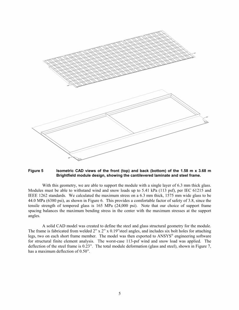
Figure 5 Isometric CAD views of the front (top) and back (bottom) of the 1.58 m x 3.68 m
Brightfield module design, showing the cantilevered laminate and steel frame.
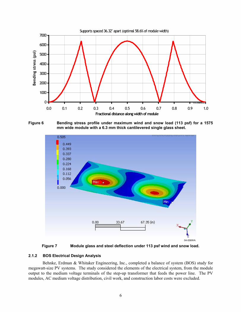
With this geometry, we are able to support the module with a single layer of 6.3 mm thick glass. Modules must be able to withstand wind and snow loads up to 5.41 kPa (113 psf), per IEC 61215 and IEEE 1262 standards. We calculated the maximum stress on a 6.3 mm thick, 1575 mm wide glass to be 44.0 MPa (6380 psi), as shown in Figure 6. This provides a comfortable factor of safety of 3.8, since the tensile strength of tempered glass is 165 MPa (24,000 psi). Note that our choice of support frame spacing balances the maximum bending stress in the center with the maximum stresses at the support angles.
A solid CAD model was created to define the steel and glass structural geometry for the module. The frame is fabricated from welded 2” x 2” x 0.19”steel angles, and includes six bolt holes for attaching legs, two on each short frame member. The model was then exported to ANSYS® engineering software for structural finite element analysis. The worst-case 113-psf wind and snow load was applied. The deflection of the steel frame is 0.23”. The total module deformation (glass and steel), shown in Figure 7, has a maximum deflection of 0.50”.
5
Supports spaced 36.32" apart (optimal 58.6% of module width)
0
1000
2000
3000
4000
5000
6000
7000
0.0 0.1 0.2 0.3 0.4 0.5 0.6 0.7 0.8 0.9 1.0Fractional distance along width of module
Bend
ing
stre
ss (
psi)
Figure 6 Bending stress profile under maximum wind and snow load (113 psf) for a 1575
mm wide module with a 6.3 mm thick cantilevered single glass sheet.
03-098WA
04-006WA Figure 7 Module glass and steel deflection under 113 psf wind and snow load.
2.1.2 BOS Electrical Design Analysis
Behnke, Erdman & Whitaker Engineering, Inc., completed a balance of system (BOS) study for megawatt-size PV systems. The study considered the elements of the electrical system, from the module output to the medium voltage terminals of the step-up transformer that feeds the power line. The PV modules, AC medium voltage distribution, civil work, and construction labor costs were excluded.
6

The study assumes a system would be built in 1 MW blocks, each with its own medium voltage (15 to 35 kV) AC interconnection. The PV array uses our nominal 5’ x 12’ 800 W modules. Wires were sized to limit the overall voltage drop to 1%. Four cases were considered: 600 VDC monopolar, ±600 VDC bipolar, 1000 VDC monopolar, and ±1000 VDC bipolar. Circuit diagrams, plant layouts, and bills of materials for 1 MW systems were designed and costs were determined for each of the four cases. 600 VDC Monopolar – This is the base case for the study and the state-of-the-art for commercial, industrial, and utility scale systems. UL-listed inverters and other components (e.g., disconnects, fuses, cabling, and combiners) with third party listings are readily available. The study assumes there are ten parallel source circuits of seven series-connected modules forming a 50 kW sub-array, four sub-arrays feeding a 200 kW inverter and transformer, and five inverters and transformers per 1 MW array. ±600 VDC Bipolar – This design takes advantage of the 2002 revision to NEC Article 690.7, which allows bipolar circuits to be considered as two 2-wire circuits when determining maximum system voltage, so long as one wire is grounded. Thus readily available 600 VDC rated components can be used for systems with inverter inputs up to 1200 VDC. No UL-listed inverters are currently available, although suitable inverter technology exists. Non-listed inverters are suitable for “behind the fence” utility applications. The design study assumes the use of a high power (1 MW) inverter. Listed high power inverters for non-utility applications could be available in twelve months time, with a commitment to purchase 10 MW or more per year. In this case, there are ten parallel source circuits of seven series-connected modules forming a 50 kW sub-array and twenty sub-arrays feeding a single 1000 kW inverter and transformer for each 1 MW array. Significant cost reductions were seen for this design compared to the base case due to the reduced number of inverters and transformers. 1000 VDC Monopolar – Modules can be rated for PV systems up to 1000 VDC under UL 1703. 1000 V BOS components (except for inverters) are available for traction, mining, and crane applications, but these components are generally not UL-listed. Listed inverters are not currently available, but suitable inverter technology exists. Load-break DC disconnects with low current ratings are not readily available, making these components more expensive than the 600 V versions. Twelve parallel source circuits of twelve series-connected modules form a 100 kW sub-array. Ten sub-arrays feed a single 1000 kW inverter and transformer for each 1 MW array. ±1000 VDC Bipolar – This design has the same advantages as the 600 V bipolar design with respect to 2-wire circuits when determining maximum system voltage ratings for components. It also has the potential, as does the 600 V bipolar design, to eliminate the inverter isolation transformer for low voltage (480 VAC) interconnections. However, it has the same drawbacks as the 1000 V monopolar design regarding the lack of available listed components. This system has the highest inverter input voltage, resulting in the lowest inverter cost. Like the 1000 V monopolar case, twelve parallel source circuits of twelve series-connected modules form a 100 kW sub-array, and ten sub-arrays feed a single 1000 kW inverter and transformer for each 1 MW array.
A cost comparison of the four BOS designs is provided in Table 3. The 600 V bipolar system has the lowest electrical BOS equipment cost, due to the availability of commercial listed components and a higher input voltage, lower cost inverter than present monopolar designs. The 1000 V bipolar system could be lower cost in the future, but currently suffers from high DC switchgear cost and availability.
7

Table 3 Electrical BOS equipment cost.
Design Case Cost ($/W) 600 VDC monopolar (base) 0.375
±600 VDC bipolar 0.266 1000 VDC monopolar 0.385
±1000 VDC bipolar 0.325 2.1.3 Production Line Definition
At 92 kg (203 lbs), the module glass is too heavy to be handled by two operators. As a result, the glass and laminates will be transported through the module production process on powered roller conveyors. A conveyor width of 68 inches was selected to handle the 62 inch wide glass. All of the assembly and test procedures are done with the module in a facedown orientation, so there is no need to turn the module over.
The module line process flow is shown in Figure 8. A preliminary production line floor plan was designed, as shown in Figure 9.
Cells In Test & SortCells
Fabricate CellStrings
Attach Buses& Diodes
Feed, Cut &Place EVA on
Glass
Wash, Rinse,Dry GlassGlass In
QC
Dark I-V &Visual
Inspection
QC
Feed, Cut &Place EVA &
Back Sheet onStrings
Laminate Trim Edges
High VoltageIsolation Test
QC
Performance(I-V) Test
QC
Modules OutInstall J-boxes
Load Glass onConveyor Buffer Glass
Inspect CellStrings
QC
Align Strings &Trim End Tabs
Place Stringson EVA/Glass
Attach Frame
04-017WA
Figure 8 Brightfield module line process flow chart.
8

Figure 9 Preliminary module production line floor plan for the large area Brightfield module. 2.2 Task 2 – Develop Cell String Inspection Process
Given the large size of the Brightfield modules, each string must be carefully inspected before lamination to ensure high yields. Our efforts in this task focused on two main activities: developing machine vision techniques for identifying visible defects in cell strings, and investigating methods for detecting microcracks in solar cells that are too small to see with a vision system. This work culminated in the design, fabrication, and testing of a full-scale prototype automated string inspection system, shown in Figure 10.
04-062WA
Figure 10 Prototype automated cell string inspection system with a string of 125 mm cells.
9

2.2.1 Visible Defect Inspections
We applied machine vision techniques to find visible defects in strings, including cell chips, visible cell cracks, cell alignment and orientation in the string, and ribbon alignment to the cell. This work began with a vision system product survey, aimed at selecting the optimum system based on capabilities, speed, cost, and ease of use. Both traditional vision systems and recently developed vision sensors were considered. After reviewing and comparing the capabilities of these systems, we selected a high-resolution DVT unit for string front and back side inspections.
Camera lenses and spacers were selected to obtain the correct field of view for front and back side inspections. Calibration plates with spot patterns were designed for pixel to real world coordinate (mm or inch) translations for front and back views. The patterns also allow corrections for lens distortion. Calibration software projects were developed for use by the operator. A Visual Basic user interface project was coded, incorporating the DVT to host PC communications protocol and display capabilities.
Polycrystalline cells present a special challenge for vision systems because they have randomly located, randomly oriented crystal grains, some of which reflect strongly under normal lighting conditions. The result is an image containing a number of bright objects of random size and location, as shown in the left image in Figure 11. These bright grains prevent the vision tools from reliably determining the locations of the cell edges and contact buses.
04-063WA
Figure 11 Vision sensor images of a 125 mm polycrystalline silicon cell using unfiltered direct lighting (left) and using two diffuse reflectors and a spectral filter (right).
Initial lighting experiments showed that bright silicon crystal grain reflections could be
eliminated by shining red LED arrays at a shallow angle onto the cell surface. However, two large, expensive LED arrays were needed to fully illuminate the cell area with sufficient brightness. After testing several alternative lighting methods, we found a lower cost approach that achieves good results. In this approach, linear fluorescent lamps shine onto diffuse reflectors on opposite sides of the cell, while a filter on the camera lens cuts out the short wavelengths responsible for most of the crystal grain reflections. The results are shown in the right image in Figure 11. The vision sensor, lamps and reflectors are shown in Figure 12.
10
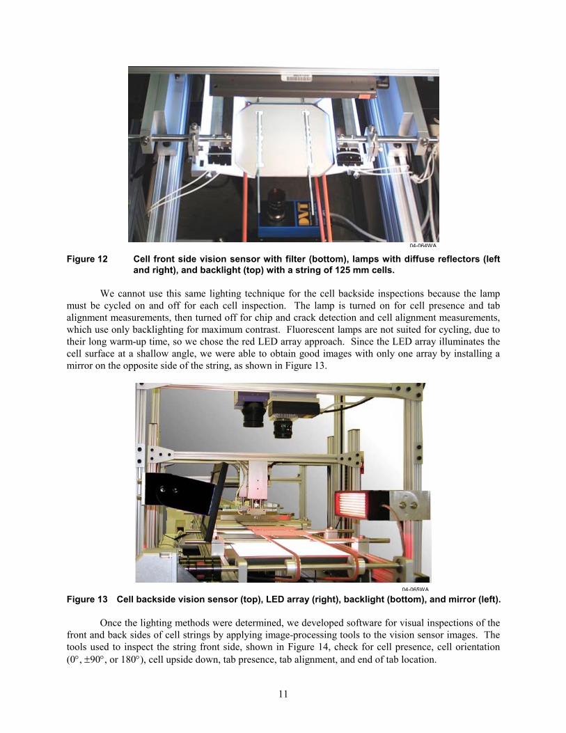
Figure 12 Cell front side vision sensor with filter (bottom), lamps with diffuse reflectors (left and right), and backlight (top) with a string of 125 mm cells.
We cannot use this same lighting technique for the cell backside inspections because the lamp
must be cycled on and off for each cell inspection. The lamp is turned on for cell presence and tab alignment measurements, then turned off for chip and crack detection and cell alignment measurements, which use only backlighting for maximum contrast. Fluorescent lamps are not suited for cycling, due to their long warm-up time, so we chose the red LED array approach. Since the LED array illuminates the cell surface at a shallow angle, we were able to obtain good images with only one array by installing a mirror on the opposite side of the string, as shown in Figure 13.
Figure 13 Cell backside vision sensor (top), LED array (right), backlight (bottom), and mirror (left).
04-064WA
04-065WA
Once the lighting methods were determined, we developed software for visual inspections of the
front and back sides of cell strings by applying image-processing tools to the vision sensor images. The tools used to inspect the string front side, shown in Figure 14, check for cell presence, cell orientation (0°, ±90°, or 180°), cell upside down, tab presence, tab alignment, and end of tab location.
11
04-066WA
Figure 14 String front side vision inspection tools on a 125 mm polycrystalline Si cell. The right image is a close-up of the tools at the top right of the cell.
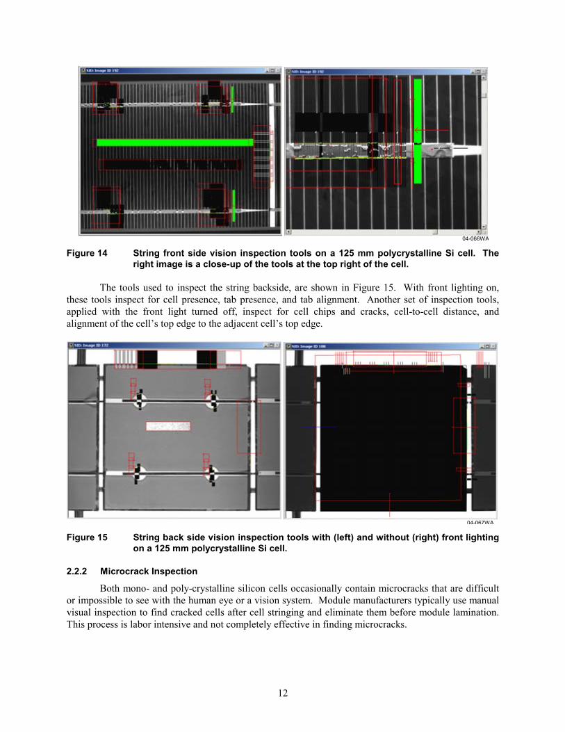
The tools used to inspect the string backside, are shown in Figure 15. With front lighting on,
these tools inspect for cell presence, tab presence, and tab alignment. Another set of inspection tools, applied with the front light turned off, inspect for cell chips and cracks, cell-to-cell distance, and alignment of the cell’s top edge to the adjacent cell’s top edge.
04-067WA
Figure 15 String back side vision inspection tools with (left) and without (right) front lighting on a 125 mm polycrystalline Si cell.
2.2.2 Microcrack Inspection
Both mono- and poly-crystalline silicon cells occasionally contain microcracks that are difficult or impossible to see with the human eye or a vision system. Module manufacturers typically use manual visual inspection to find cracked cells after cell stringing and eliminate them before module lamination. This process is labor intensive and not completely effective in finding microcracks.
12

Several potential methods for detecting microcracks in silicon cells were identified and considered:
Ultrasonics – Lassen Technologies developed a technique using a piezoelectric transducer to generate ultrasonic vibrations in a cell and detect the sonic signature of cracks. We contacted Lassen and they informed us that they are not interested in commercializing this technique.
Radiant Heating – A system using pulsed radiant heating (generated by a 3 kW flash tube) for crack detection is available from Thermosensorik GmbH in Germany. Cell cracks cause discontinuities in heat flow, and an infrared camera detects the temperature difference across the crack. This system was not selected because the cost is very high, and false crack detection is specified at <3%, which is too high for production.
Thermosonics – In this technique, ultrasonic energy causes friction heating of cracks, which an IR camera can detect as a temperature rise near the crack. Indigo Systems demonstrated their ThermoSoniXTM system at Spire on cells made from single crystal Si, cast polycrystalline Si and EFG ribbon Si. An ultrasonic horn with a blunt tip contacts the surface of a cell with a force applied by an air cylinder. A tip force of 8 to 10 lbs was applied to the cell, and 10% of full ultrasonic power was applied for 0.2 seconds. No damage was done to any of the cells during the tests.
The IR camera clearly detected microcracks approximately one second after the ultrasonic energy was applied. The system worked equally well whether the cells were face up or face down, and for gridded or solid metal back contacts. Two frames from an IR video of a test with a single crystal Si cell are shown in Figure 16. The images show the cell before and after the application of ultrasonic energy. Additional tests showed that the thermosonic system is effective at finding cracks in all three types of silicon cells.
IR heating at hairline crackUltrasonic probe
03-053WA
Figure 16 IR images of the back surface of a 125 mm square single-crystal Si solar cell, before (left) and 1 s after (right) the application of ultrasonic energy.
The ThermoSoniX system includes the software for controlling the ultrasonics and recording IR
images, but it relies on a human operator to view the images and decide if a crack is present. Vision tools and analysis software are needed to automate crack detection. This approach was not pursued further
13
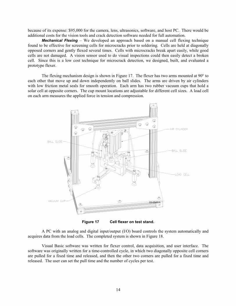
because of its expense: $95,000 for the camera, lens, ultrasonics, software, and host PC. There would be additional costs for the vision tools and crack detection software needed for full automation. Mechanical Flexing – We developed an approach based on a manual cell flexing technique found to be effective for screening cells for microcracks prior to soldering. Cells are held at diagonally opposed corners and gently flexed several times. Cells with microcracks break apart easily, while good cells are not damaged. A vision sensor used to do visual inspections could then easily detect a broken cell. Since this is a low cost technique for microcrack detection, we designed, built, and evaluated a prototype flexer.
The flexing mechanism design is shown in Figure 17. The flexer has two arms mounted at 90° to each other that move up and down independently on ball slides. The arms are driven by air cylinders with low friction metal seals for smooth operation. Each arm has two rubber vacuum cups that hold a solar cell at opposite corners. The cup mount locations are adjustable for different cell sizes. A load cell on each arm measures the applied force in tension and compression.
03-054WA
Figure 17 Cell flexer on test stand.
A PC with an analog and digital input/output (I/O) board controls the system automatically and
acquires data from the load cells. The completed system is shown in Figure 18.
Visual Basic software was written for flexer control, data acquisition, and user interface. The software was originally written for a time-controlled cycle, in which two diagonally opposite cell corners are pulled for a fixed time and released, and then the other two corners are pulled for a fixed time and released. The user can set the pull time and the number of cycles per test.
14
03-068WA
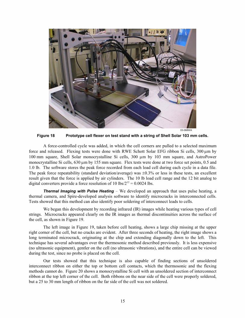
Figure 18 Prototype cell flexer on test stand with a string of Shell Solar 103 mm cells.
A force-controlled cycle was added, in which the cell corners are pulled to a selected maximum force and released. Flexing tests were done with RWE Schott Solar EFG ribbon Si cells, 300 μm by 100 mm square, Shell Solar monocrystalline Si cells, 300 μm by 103 mm square, and AstroPower monocrystalline Si cells, 630 μm by 155 mm square. Flex tests were done at two force set points, 0.5 and 1.0 lb. The software stores the peak force recorded from each load cell during each cycle in a data file. The peak force repeatability (standard deviation/average) was ±0.3% or less in these tests, an excellent result given that the force is applied by air cylinders. The 10 lb load cell range and the 12 bit analog to digital converters provide a force resolution of 10 lbs/212 = 0.0024 lbs.
Thermal Imaging with Pulse Heating – We developed an approach that uses pulse heating, a thermal camera, and Spire-developed analysis software to identify microcracks in interconnected cells. Tests showed that this method can also identify poor soldering of interconnect leads to cells.
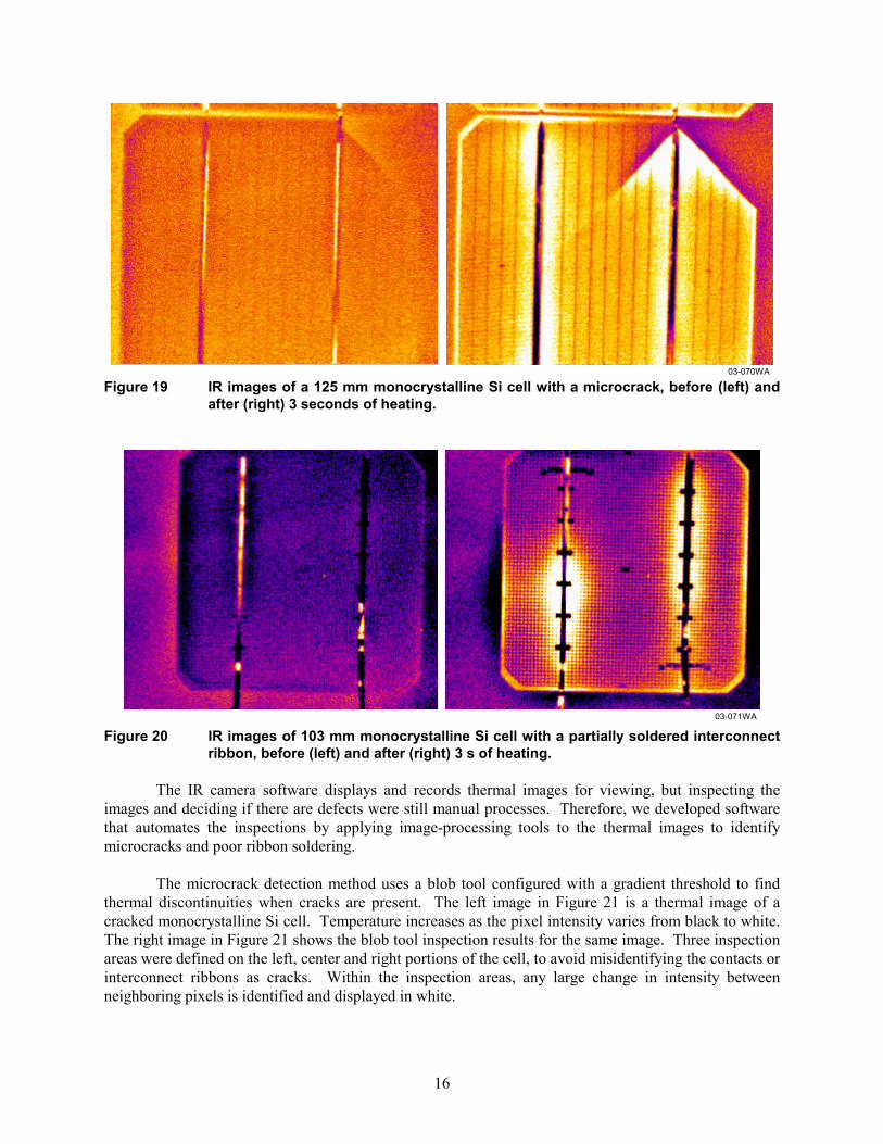
We began this development by recording infrared (IR) images while heating various types of cell strings. Microcracks appeared clearly on the IR images as thermal discontinuities across the surface of the cell, as shown in Figure 19.
The left image in Figure 19, taken before cell heating, shows a large chip missing at the upper right corner of the cell, but no cracks are evident. After three seconds of heating, the right image shows a long terminated microcrack, originating at the chip and extending diagonally down to the left. This technique has several advantages over the thermosonic method described previously. It is less expensive (no ultrasonic equipment), gentler on the cell (no ultrasonic vibrations), and the entire cell can be viewed during the test, since no probe is placed on the cell.
Our tests showed that this technique is also capable of finding sections of unsoldered interconnect ribbon on either the top or bottom cell contacts, which the thermosonic and the flexing methods cannot do. Figure 20 shows a monocrystalline Si cell with an unsoldered section of interconnect ribbon at the top left corner of the cell. Both ribbons on the near side of the cell were properly soldered, but a 25 to 30 mm length of ribbon on the far side of the cell was not soldered.
15
03-070WA
Figure 19 IR images of a 125 mm monocrystalline Si cell with a microcrack, before (left) and after (right) 3 seconds of heating.
03-071WA
Figure 20 IR images of 103 mm monocrystalline Si cell with a partially soldered interconnect ribbon, before (left) and after (right) 3 s of heating.
The IR camera software displays and records thermal images for viewing, but inspecting the
images and deciding if there are defects were still manual processes. Therefore, we developed software that automates the inspections by applying image-processing tools to the thermal images to identify microcracks and poor ribbon soldering.
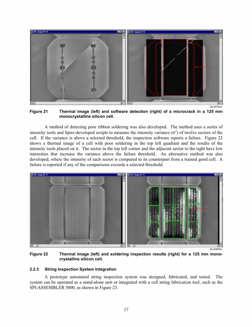
The microcrack detection method uses a blob tool configured with a gradient threshold to find thermal discontinuities when cracks are present. The left image in Figure 21 is a thermal image of a cracked monocrystalline Si cell. Temperature increases as the pixel intensity varies from black to white. The right image in Figure 21 shows the blob tool inspection results for the same image. Three inspection areas were defined on the left, center and right portions of the cell, to avoid misidentifying the contacts or interconnect ribbons as cracks. Within the inspection areas, any large change in intensity between neighboring pixels is identified and displayed in white.
16
04-007WA
Figure 21 Thermal image (left) and software detection (right) of a microcrack in a 125 mm monocrystalline silicon cell.
A method of detecting poor ribbon soldering was also developed. The method uses a series of
intensity tools and Spire-developed scripts to measure the intensity variance (σ2) of twelve sectors of the cell. If the variance is above a selected threshold, the inspection software reports a failure. Figure 22 shows a thermal image of a cell with poor soldering in the top left quadrant and the results of the intensity tools placed on it. The sector in the top left corner and the adjacent sector to the right have low intensities that increase the variance above the failure threshold. An alternative method was also developed, where the intensity of each sector is compared to its counterpart from a trained good cell. A failure is reported if any of the comparisons exceeds a selected threshold.
04-008WA
Figure 22 Thermal image (left) and soldering inspection results (right) for a 125 mm mono-crystalline silicon cell.
2.2.3 String Inspection System Integration
A prototype automated string inspection system was designed, fabricated, and tested. The system can be operated as a stand-alone unit or integrated with a cell string fabrication tool, such as the SPI-ASSEMBLER 5000, as shown in Figure 23.
17

Figure 23 String inspection system integrated with string and module assembly (plan view).
An o-ring conveyor provides string transport with maximum visibility for inspecting both sides
of the string. The conveyor and the component mounts for cameras, front lighting, backlighting, and probes are adjustable for inspecting cell sizes up to 200 mm square. A PC controls the inspection system and acquires data from the vision sensors and thermal camera through Ethernet and USB connections. The completed system is shown in Figure 24.
04-043WA
Figure 24 Cell string inspection system with a string of 125 mm cells.
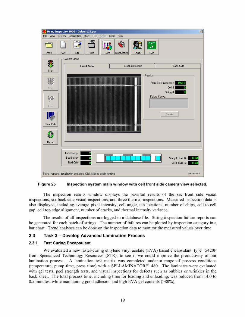
Visual Basic software was developed for system operation, diagnostics, calibration, and cell string inspections. A complete graphical user interface (GUI) was also developed. The main operating window, shown in Figure 25, includes operator controls, tab access to all three camera views, string and defect counters, an animated view of string location on the conveyor, and drop-down menus for all software functions.
18
04-069WA
Figure 25 Inspection system main window with cell front side camera view selected.
The inspection results window displays the pass/fail results of the six front side visual
inspections, six back side visual inspections, and three thermal inspections. Measured inspection data is also displayed, including average pixel intensity, cell angle, tab locations, number of chips, cell-to-cell gap, cell top edge alignment, number of cracks, and thermal intensity variance.
The results of all inspections are logged in a database file. String inspection failure reports can be generated for each batch of strings. The number of failures can be plotted by inspection category in a bar chart. Trend analyses can be done on the inspection data to monitor the measured values over time.
2.3 Task 3 – Develop Advanced Lamination Process 2.3.1 Fast Curing Encapsulant
We evaluated a new faster-curing ethylene vinyl acetate (EVA) based encapsulant, type 15420P from Specialized Technology Resources (STR), to see if we could improve the productivity of our lamination process. A lamination test matrix was completed under a range of process conditions (temperature, pump time, press time) with a SPI-LAMINATORTM 480. The laminates were evaluated with gel tests, peel strength tests, and visual inspections for defects such as bubbles or wrinkles in the back sheet. The total process time, including time for loading and unloading, was reduced from 14.0 to 8.5 minutes, while maintaining good adhesion and high EVA gel contents (>80%).
19
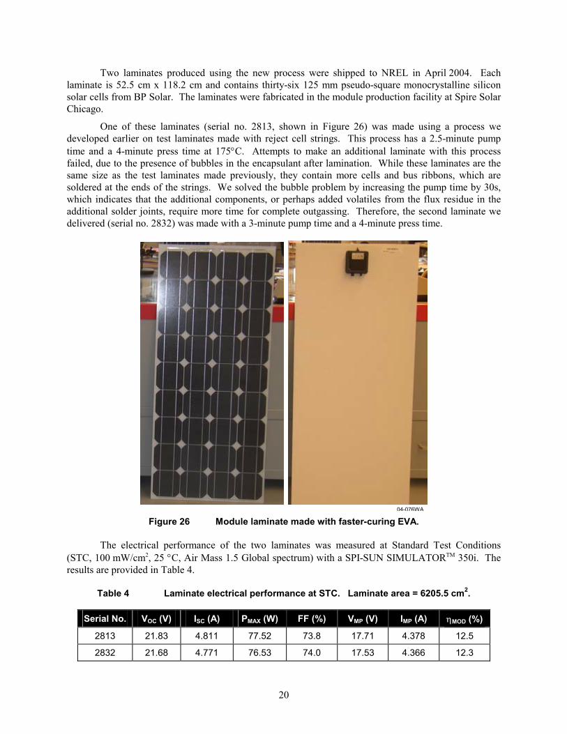
Two laminates produced using the new process were shipped to NREL in April 2004. Each laminate is 52.5 cm x 118.2 cm and contains thirty-six 125 mm pseudo-square monocrystalline silicon solar cells from BP Solar. The laminates were fabricated in the module production facility at Spire Solar Chicago.
One of these laminates (serial no. 2813, shown in Figure 26) was made using a process we developed earlier on test laminates made with reject cell strings. This process has a 2.5-minute pump time and a 4-minute press time at 175°C. Attempts to make an additional laminate with this process failed, due to the presence of bubbles in the encapsulant after lamination. While these laminates are the same size as the test laminates made previously, they contain more cells and bus ribbons, which are soldered at the ends of the strings. We solved the bubble problem by increasing the pump time by 30s, which indicates that the additional components, or perhaps added volatiles from the flux residue in the additional solder joints, require more time for complete outgassing. Therefore, the second laminate we delivered (serial no. 2832) was made with a 3-minute pump time and a 4-minute press time.
04-076WA
Figure 26 Module laminate made with faster-curing EVA.
The electrical performance of the two laminates was measured at Standard Test Conditions (STC, 100 mW/cm2, 25 °C, Air Mass 1.5 Global spectrum) with a SPI-SUN SIMULATORTM 350i. The results are provided in Table 4.
Table 4 Laminate electrical performance at STC. Laminate area = 6205.5 cm2.
Serial No. VOC (V) ISC (A) PMAX (W) FF (%) VMP (V) IMP (A) ηMOD (%)
2813 21.83 4.811 77.52 73.8 17.71 4.378 12.5
2832 21.68 4.771 76.53 74.0 17.53 4.366 12.3
20
Our standard lamination cycle with STR formulation 15295P/UF EVA is processed at 155°C with a 5.5-minute pump time and a 7-minute press time, for a total of 12.5 minutes. The new faster-curing 15420P/UF EVA, with a 3-minute pump and a 4-minute press, saves 5.5 minutes per run. Since both processes require roughly 1.5 minutes for cover opening, loading, and cover closing, the total cycle time has been reduced from 14 minutes to 8.5 minutes. As a result, production through the laminator increases from 4.3 to 7.1 runs/hour.
2.3.2 Laminator Heater Thermal Compound
Module laminators use heated platens to melt and cure the EVA encapsulant. Since the process is done in a vacuum, Spire laminators use a thermal compound to ensure good thermal conduction between the heaters and the platen. The compound is a paste that, after some years of use, can migrate away from the heater-platen interface, due to repetitive thermal cycling. If migration occurs, the temperature uniformity of the platen can degrade with time, and the platen must be rebuilt, which involves disassembly, cleaning, application of new compound, and reassembly.
We are investigating a solid thermally conductive material that may eliminate the labor and downtime required to rebuild the platen. We compared several different materials and selected a graphite composite sheet, 0.13 mm (0.005 inch) thick, with a thermal conductivity of 5 W/mK and a temperature rating of 300°C.
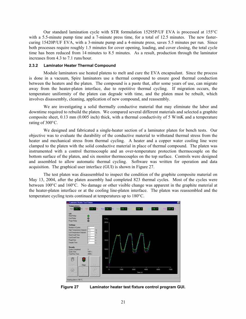
We designed and fabricated a single-heater section of a laminator platen for bench tests. Our objective was to evaluate the durability of the conductive material to withstand thermal stress from the heater and mechanical stress from thermal cycling. A heater and a copper water cooling line were clamped to the platen with the solid conductive material in place of thermal compound. The platen was instrumented with a control thermocouple and an over-temperature protection thermocouple on the bottom surface of the platen, and six monitor thermocouples on the top surface. Controls were designed and assembled to allow automatic thermal cycling. Software was written for operation and data acquisition. The graphical user interface (GUI) is shown in Figure 27.
The test platen was disassembled to inspect the condition of the graphite composite material on May 13, 2004, after the platen assembly had completed 823 thermal cycles. Most of the cycles were between 100°C and 160°C. No damage or other visible change was apparent in the graphite material at the heater-platen interface or at the cooling line-platen interface. The platen was reassembled and the temperature cycling tests continued at temperatures up to 180°C.
Figure 27 Laminator heater test fixture control program GUI.
21

Testing was completed after 2478 thermal cycles. We then disassembled the platen and found that the graphite material was worn in some areas due to mechanical stress from thermal cycling. The graphite was removed and the test platen was reassembled with our standard thermal grease. Thermal cycles were then run while monitoring the platen temperature for comparison with the graphite data. These tests showed that the temperature uniformity of our test platen is substantially better with thermal grease (±3.5°C average) than with the graphite material (±6.7°C average). This was a surprising result, given that the graphite material has a higher thermal conductivity (5 W/mK) than the thermal grease (0.95 W/mK). We suspect that the ability of the grease to flow and fill in gaps caused by irregularities in the mating surfaces is more important for uniform heat transfer in a vacuum than the difference in conductivity of the materials. Given these results, we rejected the graphite material as a possible replacement for the thermal compound. 2.4 Task 4 – Design Module Lay-up System
Concepts were developed for automating the placement of large sheets of EVA and back sheet material for module assembly prior to lamination. The Automation & Robotics Research Institute (ARRI) conducted a design for automation (DFA) analysis of the busing lay-up and back sheet feedthrough for connecting the output buses to the junction box. Most current production techniques are designed for manual assembly, and require multiple folds or splices of bus bar ribbons and the placement of insulating material to prevent shorting the buses to the cells. We devised an approach that uses a single vertical bend in the bus bar at each end of the module, a step that is easily automated and allows vertical placement of pre-slit sheet materials.
Due to the size of our large area module, careful consideration was given to automating the placement of the sheet materials. Commercial sheeters are available for dispensing materials from rolls and cutting them to length. Three different methods were considered for transferring the cut sheets onto the module: stacking on a tray followed by pick-and-place operations; winding on a tube followed by unrolling onto the module; and direct dispensing from the sheeter onto the module. 2.4.1 Stacking on a Tray
In this process, a sheeter makes an aligned stack on a tray for each material lay-up step. The trays are transported on conveyors or carts to two large pick-and-place machines that transfer the materials to the module. The first pick-and-place transfers EVA onto glass, while the second transfers EVA and back sheet over the cell strings, as shown in Figure 28.
Figure 28 Pick-and-place option for material lay-up in module production.
22
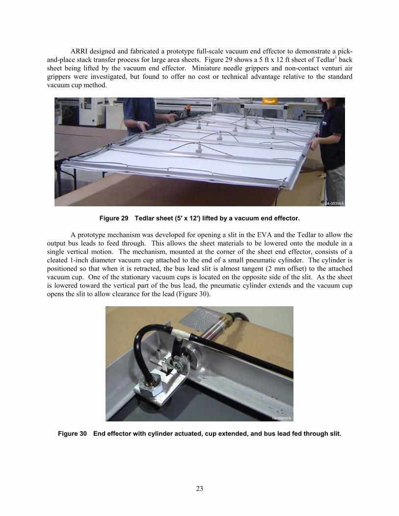
ARRI designed and fabricated a prototype full-scale vacuum end effector to demonstrate a pick-and-place stack transfer process for large area sheets. Figure 29 shows a 5 ft x 12 ft sheet of Tedlar1 back sheet being lifted by the vacuum end effector. Miniature needle grippers and non-contact venturi air grippers were investigated, but found to offer no cost or technical advantage relative to the standard vacuum cup method.
04-053WA
Figure 29 Tedlar sheet (5′ x 12′) lifted by a vacuum end effector.
A prototype mechanism was developed for opening a slit in the EVA and the Tedlar to allow the
output bus leads to feed through. This allows the sheet materials to be lowered onto the module in a single vertical motion. The mechanism, mounted at the corner of the sheet end effector, consists of a cleated 1-inch diameter vacuum cup attached to the end of a small pneumatic cylinder. The cylinder is positioned so that when it is retracted, the bus lead slit is almost tangent (2 mm offset) to the attached vacuum cup. One of the stationary vacuum cups is located on the opposite side of the slit. As the sheet is lowered toward the vertical part of the bus lead, the pneumatic cylinder extends and the vacuum cup opens the slit to allow clearance for the lead (Figure 30).
04-056WA
Figure 30 End effector with cylinder actuated, cup extended, and bus lead fed through slit.
23
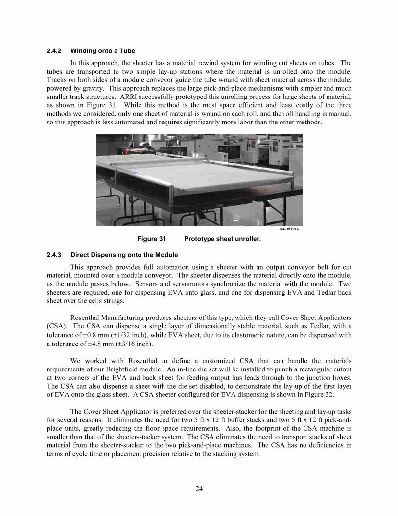
2.4.2 Winding onto a Tube
In this approach, the sheeter has a material rewind system for winding cut sheets on tubes. The tubes are transported to two simple lay-up stations where the material is unrolled onto the module. Tracks on both sides of a module conveyor guide the tube wound with sheet material across the module, powered by gravity. This approach replaces the large pick-and-place mechanisms with simpler and much smaller track structures. ARRI successfully prototyped this unrolling process for large sheets of material, as shown in Figure 31. While this method is the most space efficient and least costly of the three methods we considered, only one sheet of material is wound on each roll, and the roll handling is manual, so this approach is less automated and requires significantly more labor than the other methods.
04-081WA
Figure 31 Prototype sheet unroller. 2.4.3 Direct Dispensing onto the Module
This approach provides full automation using a sheeter with an output conveyor belt for cut material, mounted over a module conveyor. The sheeter dispenses the material directly onto the module, as the module passes below. Sensors and servomotors synchronize the material with the module. Two sheeters are required, one for dispensing EVA onto glass, and one for dispensing EVA and Tedlar back sheet over the cells strings.
Rosenthal Manufacturing produces sheeters of this type, which they call Cover Sheet Applicators (CSA). The CSA can dispense a single layer of dimensionally stable material, such as Tedlar, with a tolerance of ±0.8 mm (±1/32 inch), while EVA sheet, due to its elastomeric nature, can be dispensed with a tolerance of ±4.8 mm (±3/16 inch).
We worked with Rosenthal to define a customized CSA that can handle the materials requirements of our Brightfield module. An in-line die set will be installed to punch a rectangular cutout at two corners of the EVA and back sheet for feeding output bus leads through to the junction boxes. The CSA can also dispense a sheet with the die set disabled, to demonstrate the lay-up of the first layer of EVA onto the glass sheet. A CSA sheeter configured for EVA dispensing is shown in Figure 32.
The Cover Sheet Applicator is preferred over the sheeter-stacker for the sheeting and lay-up tasks for several reasons. It eliminates the need for two 5 ft x 12 ft buffer stacks and two 5 ft x 12 ft pick-and-place units, greatly reducing the floor space requirements. Also, the footprint of the CSA machine is smaller than that of the sheeter-stacker system. The CSA eliminates the need to transport stacks of sheet material from the sheeter-stacker to the two pick-and-place machines. The CSA has no deficiencies in terms of cycle time or placement precision relative to the stacking system.
24
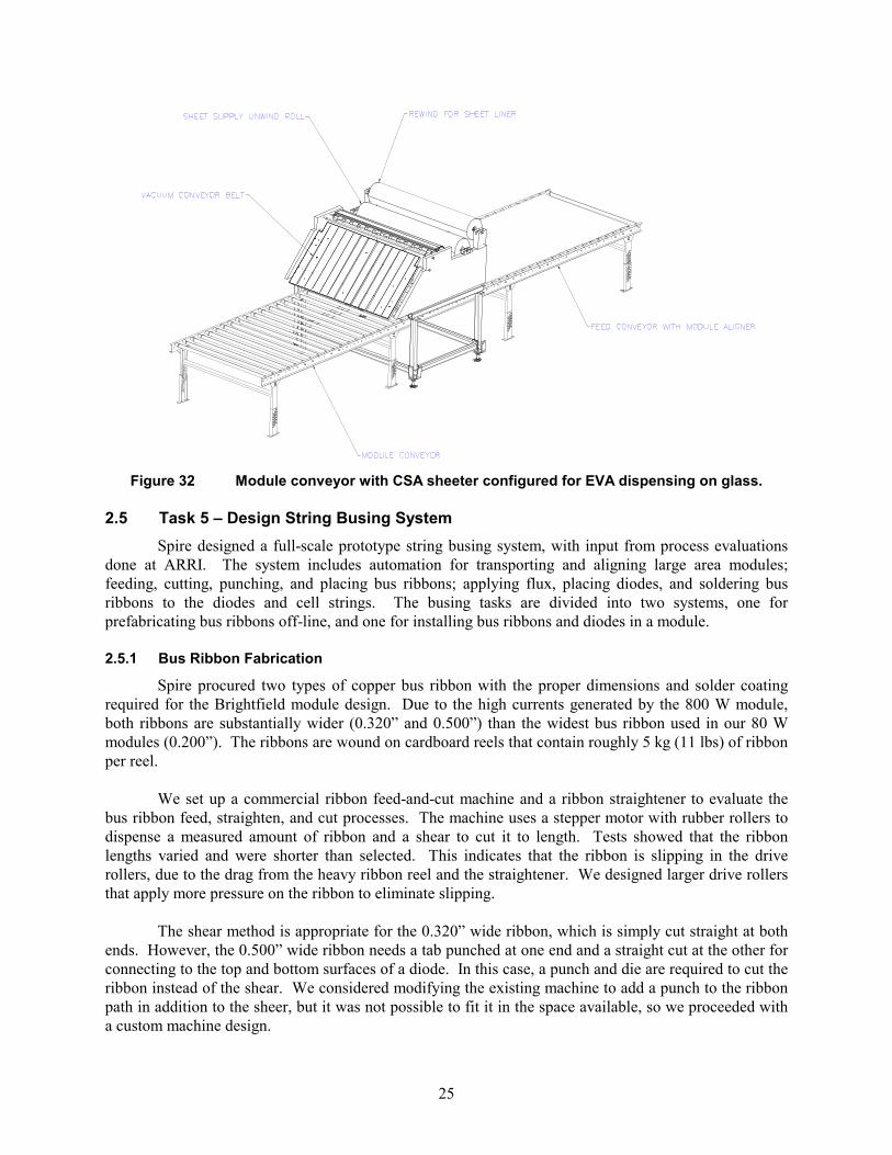
Figure 32 Module conveyor with CSA sheeter configured for EVA dispensing on glass.
2.5 Task 5 – Design String Busing System
Spire designed a full-scale prototype string busing system, with input from process evaluations done at ARRI. The system includes automation for transporting and aligning large area modules; feeding, cutting, punching, and placing bus ribbons; applying flux, placing diodes, and soldering bus ribbons to the diodes and cell strings. The busing tasks are divided into two systems, one for prefabricating bus ribbons off-line, and one for installing bus ribbons and diodes in a module. 2.5.1 Bus Ribbon Fabrication
Spire procured two types of copper bus ribbon with the proper dimensions and solder coating required for the Brightfield module design. Due to the high currents generated by the 800 W module, both ribbons are substantially wider (0.320” and 0.500”) than the widest bus ribbon used in our 80 W modules (0.200”). The ribbons are wound on cardboard reels that contain roughly 5 kg (11 lbs) of ribbon per reel.
We set up a commercial ribbon feed-and-cut machine and a ribbon straightener to evaluate the bus ribbon feed, straighten, and cut processes. The machine uses a stepper motor with rubber rollers to dispense a measured amount of ribbon and a shear to cut it to length. Tests showed that the ribbon lengths varied and were shorter than selected. This indicates that the ribbon is slipping in the drive rollers, due to the drag from the heavy ribbon reel and the straightener. We designed larger drive rollers that apply more pressure on the ribbon to eliminate slipping.
The shear method is appropriate for the 0.320” wide ribbon, which is simply cut straight at both ends. However, the 0.500” wide ribbon needs a tab punched at one end and a straight cut at the other for connecting to the top and bottom surfaces of a diode. In this case, a punch and die are required to cut the ribbon instead of the shear. We considered modifying the existing machine to add a punch to the ribbon path in addition to the sheer, but it was not possible to fit it in the space available, so we proceeded with a custom machine design.
25
Once the bus ribbon is cut or punched to length, it is loaded into a tray that will hold a stack of ribbons. Most of the ribbon length is pushed into the tray by the drive rollers, but the last several inches remains in the shear or die set. We designed a two-axis pneumatic pick-and-place mechanism with a vacuum cup to pick up the trailing end of the ribbon, advance it so it is completely over the tray, and drop it into the tray.
It is important for the ribbon to remain relatively flat for stacking in the tray and for accurate assembly in the module. We were concerned that as the ribbon is pushed into the tray, the edges of the ribbon might rub on the tray sidewalls and bend, so we fabricated a prototype tray for 0.500” wide ribbon. Tests showed that the drive rollers reliably pushed the ribbon into the tray without distortion. Tests simulating the final pick-and-place operation were also successful in maintaining flat ribbon.
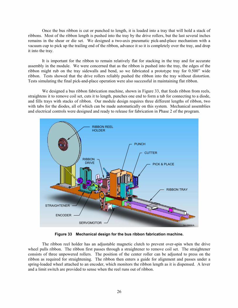
We designed a bus ribbon fabrication machine, shown in Figure 33, that feeds ribbon from reels, straightens it to remove coil set, cuts it to length, punches one end to form a tab for connecting to a diode, and fills trays with stacks of ribbon. Our module design requires three different lengths of ribbon, two with tabs for the diodes, all of which can be made automatically on this system. Mechanical assemblies and electrical controls were designed and ready to release for fabrication in Phase 2 of the program.
RIBBON REEL HOLDER
PUNCH
CUTTER
RIBBON DRIVE PICK & PLACE
RIBBON TRAY
STRAIGHTENER
ENCODER
SERVOMOTOR04-088WA
Figure 33 Mechanical design for the bus ribbon fabrication machine.
The ribbon reel holder has an adjustable magnetic clutch to prevent over-spin when the drive
wheel pulls ribbon. The ribbon first passes through a straightener to remove coil set. The straightener consists of three unpowered rollers. The position of the center roller can be adjusted to press on the ribbon as required for straightening. The ribbon then enters a guide for alignment and passes under a spring-loaded wheel attached to an encoder, which monitors the ribbon length as it is dispensed. A lever and a limit switch are provided to sense when the reel runs out of ribbon.
26
The ribbon drive assembly consists of a spring-loaded pinch roller and a drive roller powered by a servomotor. A lever and cam lift the pinch roller up above the drive roller to simplify ribbon threading when a new ribbon reel is loaded.
The ribbon punch consists of a stationary die and an air-driven clamp and punch assembly. When the air cylinder is extended, the clamp holds the ribbon in place on both sides of the die while the punch cuts a tab shape on one end of the ribbon and a straight cut on the other end. The tab shape allows a connection to be made to the top surface of the diode without shorting to the bus ribbon connected to the bottom surface of the diode. The ribbon cutter assembly has a stationary blade and an air-driven blade that cuts across the ribbon as it moves down, like a paper cutter. The moving blade is spring-loaded against the stationary blade for self-alignment.
Once the bus ribbon is cut or punched to length, it is loaded into a tray that holds a stack of ribbons. Most of the ribbon length is pushed into the tray by the drive rollers, but the last several inches remains in the shear or die set. A two-axis pneumatic pick-and-place mechanism with a vacuum cup picks up the trailing end of the ribbon, advances it so it is completely over the tray, and drops it into the tray. 2.5.2 Bus Ribbon and Diode Installation – SCARA Robot Approach
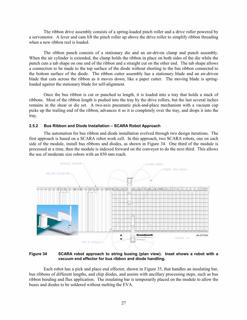
The automation for bus ribbon and diode installation evolved through two design iterations. The first approach is based on a SCARA robot work cell. In this approach, two SCARA robots, one on each side of the module, install bus ribbons and diodes, as shown in Figure 34. One third of the module is processed at a time, then the module is indexed forward on the conveyor to do the next third. This allows the use of moderate size robots with an 850 mm reach.
04-077WA
Figure 34 SCARA robot approach to string busing (plan view). Inset shows a robot with a vacuum end effector for bus ribbon and diode handling.
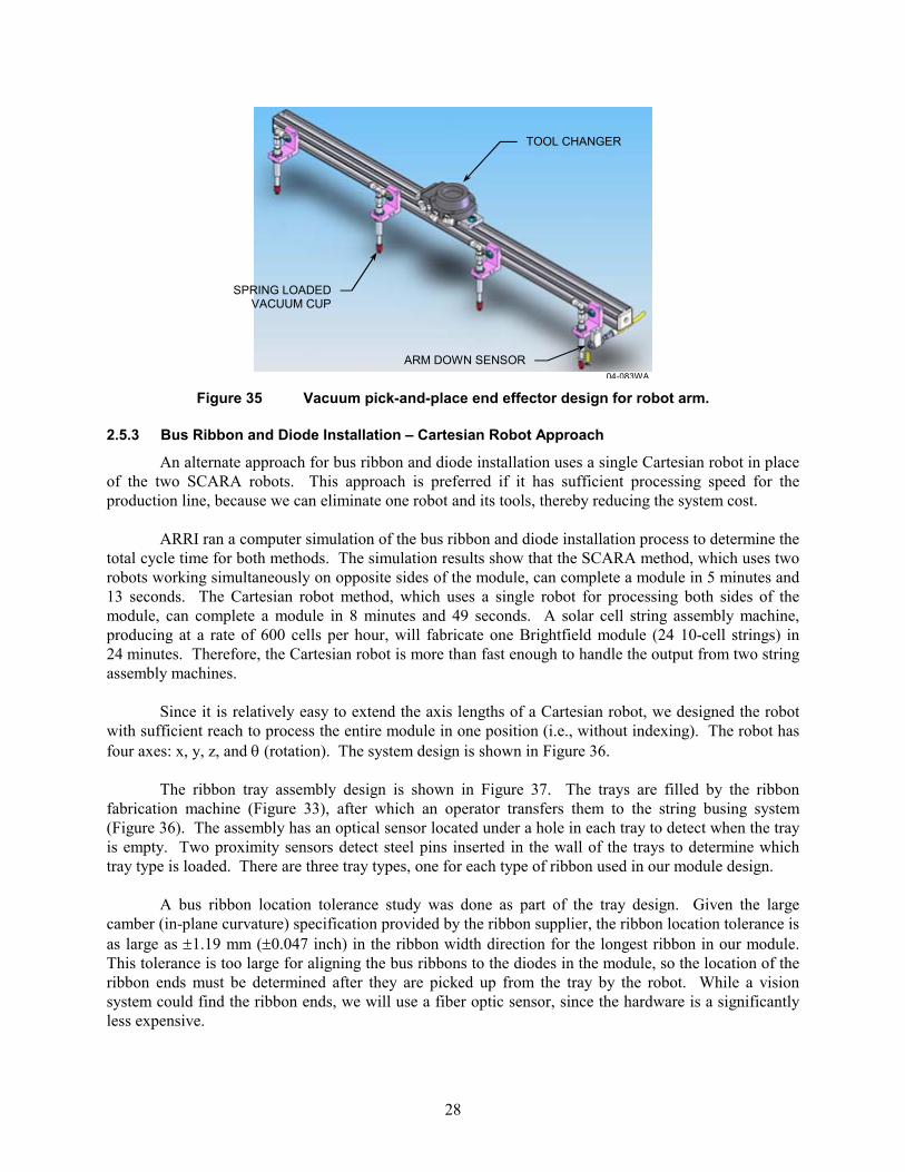
Each robot has a pick and place end effector, shown in Figure 35, that handles an insulating bar,
bus ribbons of different lengths, and chip diodes, and assists with ancillary processing steps, such as bus ribbon bending and flux application. The insulating bar is temporarily placed on the module to allow the buses and diodes to be soldered without melting the EVA.
27
TOOL CHANGER
SPRING LOADED VACUUM CUP
ARM DOWN SENSOR
04-083WA
Figure 35 Vacuum pick-and-place end effector design for robot arm. 2.5.3 Bus Ribbon and Diode Installation – Cartesian Robot Approach
An alternate approach for bus ribbon and diode installation uses a single Cartesian robot in place of the two SCARA robots. This approach is preferred if it has sufficient processing speed for the production line, because we can eliminate one robot and its tools, thereby reducing the system cost.
ARRI ran a computer simulation of the bus ribbon and diode installation process to determine the total cycle time for both methods. The simulation results show that the SCARA method, which uses two robots working simultaneously on opposite sides of the module, can complete a module in 5 minutes and 13 seconds. The Cartesian robot method, which uses a single robot for processing both sides of the module, can complete a module in 8 minutes and 49 seconds. A solar cell string assembly machine, producing at a rate of 600 cells per hour, will fabricate one Brightfield module (24 10-cell strings) in 24 minutes. Therefore, the Cartesian robot is more than fast enough to handle the output from two string assembly machines.
Since it is relatively easy to extend the axis lengths of a Cartesian robot, we designed the robot with sufficient reach to process the entire module in one position (i.e., without indexing). The robot has four axes: x, y, z, and θ (rotation). The system design is shown in Figure 36.
The ribbon tray assembly design is shown in Figure 37. The trays are filled by the ribbon fabrication machine (Figure 33), after which an operator transfers them to the string busing system (Figure 36). The assembly has an optical sensor located under a hole in each tray to detect when the tray is empty. Two proximity sensors detect steel pins inserted in the wall of the trays to determine which tray type is loaded. There are three tray types, one for each type of ribbon used in our module design.
A bus ribbon location tolerance study was done as part of the tray design. Given the large camber (in-plane curvature) specification provided by the ribbon supplier, the ribbon location tolerance is as large as ±1.19 mm (±0.047 inch) in the ribbon width direction for the longest ribbon in our module. This tolerance is too large for aligning the bus ribbons to the diodes in the module, so the location of the ribbon ends must be determined after they are picked up from the tray by the robot. While a vision system could find the ribbon ends, we will use a fiber optic sensor, since the hardware is a significantly less expensive.
28

4-AXIS CARTESIAN ROBOT
BUS RIBBON TRAY
FLUX APPLICATOR
DIODE PACK
BUS RIBBON TRAY
MODULE
INSULATOR BAR
END EFFECTOR
ROLLER CONVEYOR WITH MODULE ALIGNER
RIBBON BENDER
Figure 36 Cartesian robot approach to string busing (perspective view).
RIBBON TRAY, 1 OF 3 TYPES
TRAY EMPTY SENSOR
TRAY TYPE SENSORS 04-090WA
Figure 37 Bus ribbon tray assembly (supporting table not shown).
The robot end-effector design was reviewed and we were able to eliminate the tool changer by mounting the pick-and-place hardware and two soldering tools on the same end effector, as shown in Figure 38. Eliminating the tool changer saves process time, end-effector complexity, and cost.
The output bus ribbons at opposite ends of the module are bent up at a 90° angle to extend through the EVA and back sheet. A simple bus ribbon bending tool was prototyped at ARRI. The process sequence with ARRI’s tool is illustrated in Figure 39. When the robot picks up an output bus, it places the end of the bus in a slot in the bending tool. A guided air cylinder pushes a plate over the ribbon to form a 90° bend. After the air cylinder retracts, the robot removes the ribbon from the tool and places it on the module.
29
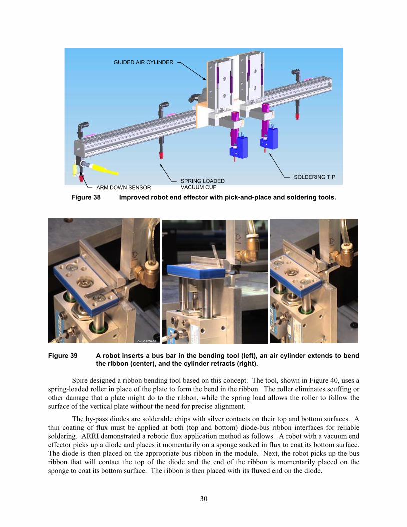
GUIDED AIR CYLINDER
SOLDERING TIP
SPRING LOADED VACUUM CUP ARM DOWN SENSOR
Figure 38 Improved robot end effector with pick-and-place and soldering tools.
04-057WA
Figure 39 A robot inserts a bus bar in the bending tool (left), an air cylinder extends to bend
the ribbon (center), and the cylinder retracts (right).
Spire designed a ribbon bending tool based on this concept. The tool, shown in Figure 40, uses a spring-loaded roller in place of the plate to form the bend in the ribbon. The roller eliminates scuffing or other damage that a plate might do to the ribbon, while the spring load allows the roller to follow the surface of the vertical plate without the need for precise alignment.
The by-pass diodes are solderable chips with silver contacts on their top and bottom surfaces. A thin coating of flux must be applied at both (top and bottom) diode-bus ribbon interfaces for reliable soldering. ARRI demonstrated a robotic flux application method as follows. A robot with a vacuum end effector picks up a diode and places it momentarily on a sponge soaked in flux to coat its bottom surface. The diode is then placed on the appropriate bus ribbon in the module. Next, the robot picks up the bus ribbon that will contact the top of the diode and the end of the ribbon is momentarily placed on the sponge to coat its bottom surface. The ribbon is then placed with its fluxed end on the diode.
30

BEVELLED RIBBON
SLOT
SPRING LOADED ROLLER
GUIDED AIR CYLINDER
Figure 40 Ribbon bender, Spire design.
Spire then designed a flux applicator to implement this process. The applicator, shown in Figure
41, has a small flux reservoir, a float switch, a peristaltic pump, and a sponge. The float switch and the pump maintain a constant level of flux in the reservoir, roughly at the mid-point of the sponge thickness.
FLOAT SWITCH
SPONGE
Figure 41 Flux applicator (left) and diode assembly in the module (right).
31

2.5.4 Automated Soldering Process Development
ARRI investigated reflow soldering techniques for soldering the bus ribbons to the diodes and cell strings. ARRI worked with Unitek Miyachi on pulsed hot bar reflow soldering equipment selection and design of a customized thermode for the soldering requirements specific to the Brightfield module, specifically the string-bus and bus-diode-bus joints. To simplify the soldering process both in terms of cycle time and cost, an effort was made to design a thermode head that is suitable for both joint types.
String-Bus Soldering: Due to the large number (96) of string-to-bus joints on the Brightfield module, a two-pronged thermode is recommended so that the two ribbons at the end of each cell string can be soldered in a single step. According to Unitek’s recommendation, a thermode head can be up to 130 mm wide and still maintain a constant temperature across the length of the head. The string lay-out on the module requires an 81.6 mm wide thermode head, well under the 130 mm limit. Testing at ARRI on string-to-bus joints showed that sufficiently sound joints can be formed with a thermode contact area of 2.2 mm × 3.0 mm. Each prong of the Unitek solder head would have dimensions of 7.2 mm × 3.0 mm, allowing for a variation in the position of the string on the bus of ±2.5 mm. A suggested thermode design is shown in Figure 42.
04-091WA
Figure 42 Preliminary thermode design for string-bus and bus-diode-bus joints (dimensions in mm). Thickness is 3 mm.
Bus-Diode Bus Soldering: ARRI sent tabbed, fluxed bus bars and diodes to Unitek Miyachi along with detailed drawings, and requested that they perform tests to determine what would be required (thermode design, power supply model, and reflow process) to form the bus-diode-bus joint in a single step. Unitek was able to solder the diode between the two bus bars, but did so using a two-step soldering process. Based on their testing, Unitek concluded that in order to form the bus-diode-bus joint in a single step, heating from both the top and bottom would be required. Unfortunately, this is not compatible with our top-down module assembly approach, and it would almost double the cost of the soldering system due to the need for a second high current power supply.
ARRI continued feasibility testing on the bus-diode-bus joints using a temperature controlled industrial soldering iron as the heating source. Using a reflow temperature of 300 ºC and a reflow time of 7 s, it was possible to obtain good solder bonds to the bus bars on both sides of the diode. With this method, the heat was applied only from the top.
The main drawback with a soldering iron is that it has no means for holding the solder joint in contact while the solder cools. This problem was recognized by Spire when we first started developing automated soldering equipment for solar cells twenty-five years ago. At that time, we invented a unique soldering tip that operates at a constant temperature and has a built-in pin that holds the joint in contact until the solder freezes. A small cartridge heater heats the soldering tip, shown in Figure 43, while its temperature is monitored by a thermocouple. The heated tip and the cooling pin are spring loaded for compliance with the soldered parts.
32
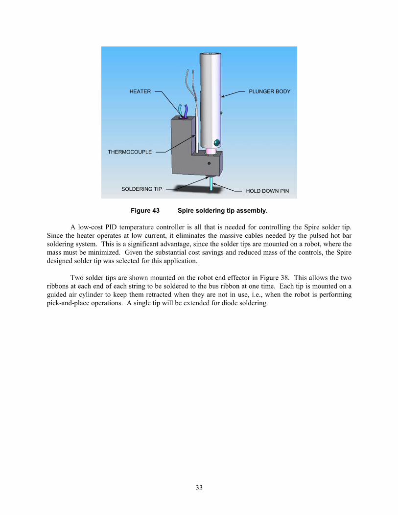
HOLD DOWN PIN
HEATER
THERMOCOUPLE
PLUNGER BODY
SOLDERING TIP
Figure 43 Spire soldering tip assembly.
A low-cost PID temperature controller is all that is needed for controlling the Spire solder tip.
Since the heater operates at low current, it eliminates the massive cables needed by the pulsed hot bar soldering system. This is a significant advantage, since the solder tips are mounted on a robot, where the mass must be minimized. Given the substantial cost savings and reduced mass of the controls, the Spire designed solder tip was selected for this application.
Two solder tips are shown mounted on the robot end effector in Figure 38. This allows the two ribbons at each end of each string to be soldered to the bus ribbon at one time. Each tip is mounted on a guided air cylinder to keep them retracted when they are not in use, i.e., when the robot is performing pick-and-place operations. A single tip will be extended for diode soldering.
33
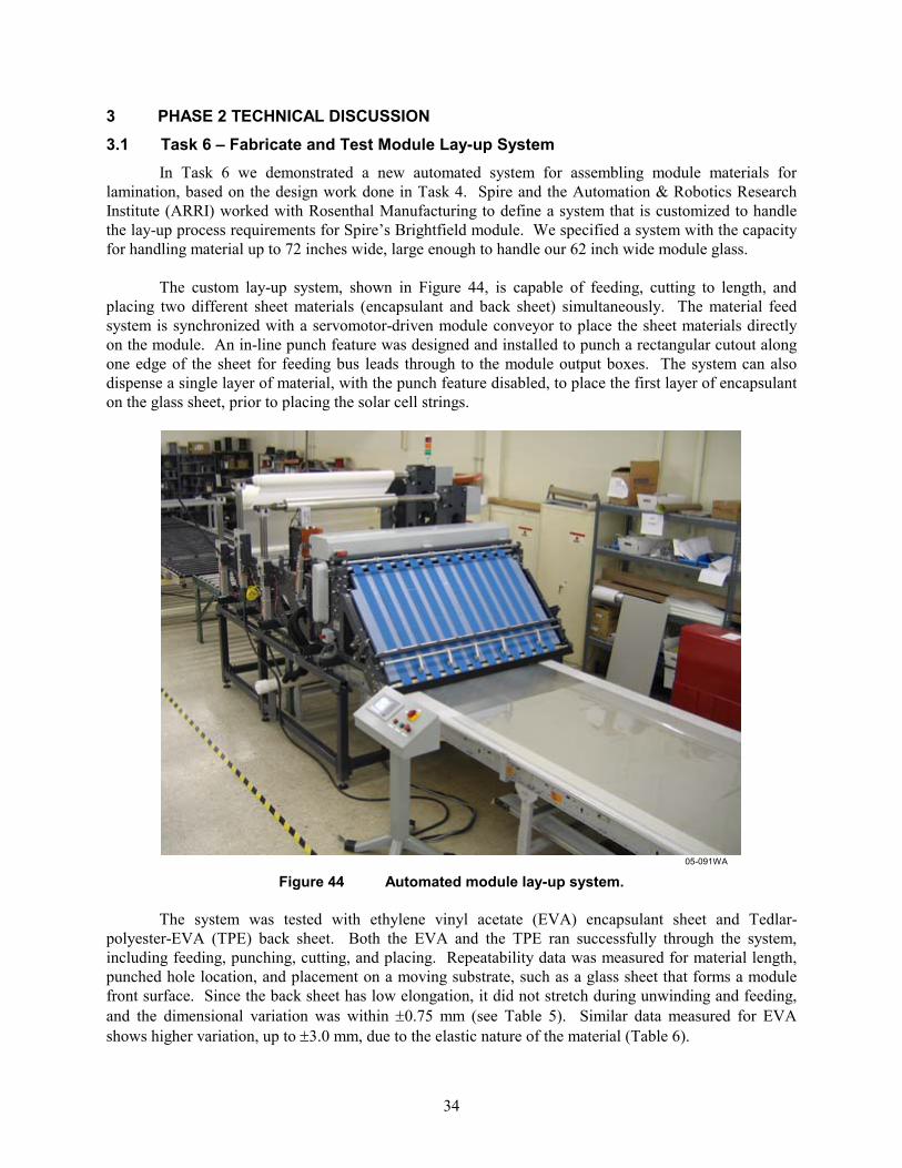
3 PHASE 2 TECHNICAL DISCUSSION
3.1 Task 6 – Fabricate and Test Module Lay-up System In Task 6 we demonstrated a new automated system for assembling module materials for
lamination, based on the design work done in Task 4. Spire and the Automation & Robotics Research Institute (ARRI) worked with Rosenthal Manufacturing to define a system that is customized to handle the lay-up process requirements for Spire’s Brightfield module. We specified a system with the capacity for handling material up to 72 inches wide, large enough to handle our 62 inch wide module glass.
The custom lay-up system, shown in Figure 44, is capable of feeding, cutting to length, and placing two different sheet materials (encapsulant and back sheet) simultaneously. The material feed system is synchronized with a servomotor-driven module conveyor to place the sheet materials directly on the module. An in-line punch feature was designed and installed to punch a rectangular cutout along one edge of the sheet for feeding bus leads through to the module output boxes. The system can also dispense a single layer of material, with the punch feature disabled, to place the first layer of encapsulant on the glass sheet, prior to placing the solar cell strings.
05-091WA
Figure 44 Automated module lay-up system.
The system was tested with ethylene vinyl acetate (EVA) encapsulant sheet and Tedlar-polyester-EVA (TPE) back sheet. Both the EVA and the TPE ran successfully through the system, including feeding, punching, cutting, and placing. Repeatability data was measured for material length, punched hole location, and placement on a moving substrate, such as a glass sheet that forms a module front surface. Since the back sheet has low elongation, it did not stretch during unwinding and feeding, and the dimensional variation was within ±0.75 mm (see Table 5). Similar data measured for EVA shows higher variation, up to ±3.0 mm, due to the elastic nature of the material (Table 6).
34

Table 5 Dimensional variations in sheet placement, cut length, and punch locations for nominal 2540 mm long TPE sheets.
Placement (mm) Length (mm) Location (mm)
Run # Left Right Left Right Punch #1 Punch #2 1 461.0 462.0 2542.0 2542.0 9.0 2448.0 2 462.5 461.0 2541.5 2542.0 8.0 2447.5 3 462.5 462.0 2542.0 2541.5 8.0 2447.5 4 462.5 462.0 2541.0 2541.5 8.0 2447.5 5 462.0 462.0 2541.5 2541.0 8.5 2447.0 6 462.0 462.0 2542.0 2542.0 8.0 2447.5
Average 462.1 461.8 2541.7 2541.7 8.3 2447.5 Max - min 1.5 1.0 1.0 1.0 1.0 1.0
Table 6 Dimensional variations in sheet placement, cut length, and punch locations for
nominal 2540 mm long EVA sheets.
Placement (mm) Length (mm) Location (mm) Run # Left Right Left Right Punch #1 Punch #2
1 467.0 467.0 2495.0 2496.0 12.0 2408.0 2 468.0 470.0 2494.0 2495.0 12.0 2406.0 3 466.0 467.0 2495.0 2495.0 12.0 2407.0 4 468.0 470.0 2493.0 2494.0 12.0 2406.0 5 465.0 468.0 2494.0 2495.0 13.0 2408.0 6 469.0 472.0 2494.0 2494.0 12.0 2406.0 7 469.0 470.0 2495.0 2495.0 13.0 2408.0 8 471.0 473.0 2493.0 2491.0 13.0 2405.0 9 469.0 470.0 2492.0 2493.0 13.0 2404.0 10 470.0 471.0 2493.0 2493.0 13.0 2405.0
Average 468.2 469.8 2493.8 2494.1 12.5 2406.3 Max - min 6.0 6.0 3.0 5.0 1.0 4.0
We found that EVA stretches in the machine length direction during feeding and shrinks after
cutting, resulting in a shorter cut length than expected. The observed shrinkage was 1.8% of the sheet length. For the module’s front EVA layer, where only one layer is being dispensed, we can compensate for the amount of shrinkage by adding this percentage to the desired length. For the back layer, the shrinkage causes misalignment in the punched holes and the cut sheet lengths between the EVA and the TPE. This problem can be solved by using an EVA-on-fiberglass material, which has much lower elongation than EVA alone. This is a standard material used behind the cells in Spire’s modules.
We tested the lay-up machine with a roll of EVA-on-fiberglass material to compare with the EVA material. The EVA-on-fiberglass ran successfully through the system, including feeding, punching, cutting, and placing. The EVA-on-fiberglass showed much less stretch during feeding than EVA alone.
Our original punch design called for a 25 mm square hole, large enough so that cut sheets could be fed from the top down over an output bus ribbon that is bent up from the surface of the module at a 90° angle. Upon review, we realized that this results in an area with no encapsulant or back sheet behind a section of the bus ribbon and an edge of a solar cell. While a terminal box will cover the hole, the design provides inferior environmental protection for the cell and the bus ribbon.
35
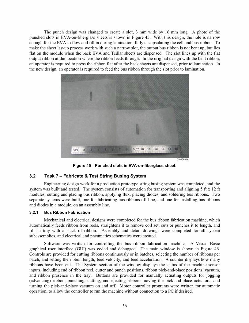
The punch design was changed to create a slot, 3 mm wide by 16 mm long. A photo of the punched slots in EVA-on-fiberglass sheets is shown in Figure 45. With this design, the hole is narrow enough for the EVA to flow and fill in during lamination, fully encapsulating the cell and bus ribbon. To make the sheet lay-up process work with such a narrow slot, the output bus ribbon is not bent up, but lies flat on the module when the back EVA and Tedlar sheets are dispensed. The slot lines up with the flat output ribbon at the location where the ribbon feeds through. In the original design with the bent ribbon, an operator is required to press the ribbon flat after the back sheets are dispensed, prior to lamination. In the new design, an operator is required to feed the bus ribbon through the slot prior to lamination.
05-056WA
Figure 45 Punched slots in EVA-on-fiberglass sheet. 3.2 Task 7 – Fabricate & Test String Busing System
Engineering design work for a production prototype string busing system was completed, and the system was built and tested. The system consists of automation for transporting and aligning 5 ft x 12 ft modules, cutting and placing bus ribbon, applying flux, placing diodes, and soldering bus ribbons. Two separate systems were built, one for fabricating bus ribbons off-line, and one for installing bus ribbons and diodes in a module, on an assembly line.
3.2.1 Bus Ribbon Fabrication
Mechanical and electrical designs were completed for the bus ribbon fabrication machine, which automatically feeds ribbon from reels, straightens it to remove coil set, cuts or punches it to length, and fills a tray with a stack of ribbon. Assembly and detail drawings were completed for all system subassemblies, and electrical and pneumatics schematics were created.
Software was written for controlling the bus ribbon fabrication machine. A Visual Basic graphical user interface (GUI) was coded and debugged. The main window is shown in Figure 46. Controls are provided for cutting ribbons continuously or in batches, selecting the number of ribbons per batch, and setting the ribbon length, feed velocity, and feed acceleration. A counter displays how many ribbons have been cut. The System section of the window displays the status of the machine sensor inputs, including end of ribbon reel, cutter and punch positions, ribbon pick-and-place positions, vacuum, and ribbon presence in the tray. Buttons are provided for manually actuating outputs for jogging (advancing) ribbon; punching, cutting, and ejecting ribbon; moving the pick-and-place actuators; and turning the pick-and-place vacuum on and off. Motor controller programs were written for automatic operation, to allow the controller to run the machine without connection to a PC if desired.
36
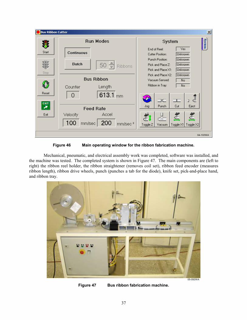
04-102WA
Figure 46 Main operating window for the ribbon fabrication machine.
Mechanical, pneumatic, and electrical assembly work was completed, software was installed, and
the machine was tested. The completed system is shown in Figure 47. The main components are (left to right) the ribbon reel holder, the ribbon straightener (removes coil set), ribbon feed encoder (measures ribbon length), ribbon drive wheels, punch (punches a tab for the diode), knife set, pick-and-place hand, and ribbon tray.
05-092WA
Figure 47 Bus ribbon fabrication machine.
37

3.2.2 Bus Ribbon and Diode Installation
Mechanical and electrical designs were completed for the bus ribbon and diode installation system, which automatically picks, aligns, and places bus ribbons and diodes, applies no-clean flux for diode soldering, and solders bus ribbons to diodes and string ribbons. Mechanical assembly and detail drawings were completed for all system subassemblies, and electrical and pneumatics schematics were created.
A large four-axis (x, y, z, and θ) Cartesian robot was specified. A CAD model of the robot is shown in Figure 48. The robot can travel 3935 mm in the x axis, 2250 mm in the y axis, and 150 mm in the z axis. Servomotors drive all four axes. The x and y axes have belt driven slides, the z axis has a lead screw, guide rods, and a brake, and the θ axis has a 127 mm diameter rotary table.
Z-AXIS
Y-AXIS X-AXIS
θ-AXIS
04-103WA
Figure 48 CAD model of four-axis Cartesian robot for busing assembly.
An end-effector was designed for the robot, including a safety clutch, a vacuum pick-and-place
arm, and two soldering tips. The robot end-effector is shown in Figure 49. The clutch stops all robot motion in the event of a collision that applies torque on the end-effector. Each solder tip assembly includes a vertical air cylinder to move the solder tip below the vacuum cups during soldering, an air jet for rapid solder joint cooling, a heated spring-loaded solder tip, and a spring-loaded pin for holding the solder joint in contact while the solder freezes.
Mechanical and electrical assembly of the busing system was completed, as shown in Figure 50. A large 1.68 m x 6.10 m (66 inch x 240 inch) roller conveyor and a 4-axis Cartesian robot were installed on a steel frame. A module stop assembly, two pneumatic module aligner assemblies, and three roller lift assemblies were built and installed on the conveyor for module alignment.
Tooling plates were installed on the frame on both sides of the conveyor. The two rear tooling plates hold a solder tip cleaner and three bus insulators for rear bus soldering. The robot places these reusable insulators under the bus ribbons to keep the EVA encapsulant from melting during soldering. The two front tooling plates hold three bus insulators for the front buses, seven bus ribbon trays (two short and two long trays for the front buses, and three trays for the rear buses), two diode pack retainers, and two flux applicator assemblies. A diode pack retainer, ribbon tray assembly, and flux applicator are shown in Figure 51. Each ribbon tray assembly has an optical sensor to signal when the tray is empty. Each flux applicator has a float switch connected to a flux supply pump to maintain the proper flux level.
38

05-070WA
Figure 49 Robot end effector with soldering heads and vacuum pick-up arm.
05-068WA
Figure 50 Module-size aluminum sheet on the automated busing system.
39
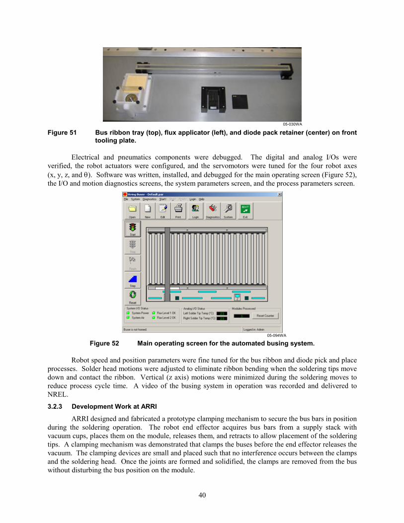
05-030WA
Figure 51 Bus ribbon tray (top), flux applicator (left), and diode pack retainer (center) on front tooling plate.
Electrical and pneumatics components were debugged. The digital and analog I/Os were
verified, the robot actuators were configured, and the servomotors were tuned for the four robot axes (x, y, z, and θ). Software was written, installed, and debugged for the main operating screen (Figure 52), the I/O and motion diagnostics screens, the system parameters screen, and the process parameters screen.
05-094WA
Figure 52 Main operating screen for the automated busing system.
Robot speed and position parameters were fine tuned for the bus ribbon and diode pick and place processes. Solder head motions were adjusted to eliminate ribbon bending when the soldering tips move down and contact the ribbon. Vertical (z axis) motions were minimized during the soldering moves to reduce process cycle time. A video of the busing system in operation was recorded and delivered to NREL.
3.2.3 Development Work at ARRI
ARRI designed and fabricated a prototype clamping mechanism to secure the bus bars in position during the soldering operation. The robot end effector acquires bus bars from a supply stack with vacuum cups, places them on the module, releases them, and retracts to allow placement of the soldering tips. A clamping mechanism was demonstrated that clamps the buses before the end effector releases the vacuum. The clamping devices are small and placed such that no interference occurs between the clamps and the soldering head. Once the joints are formed and solidified, the clamps are removed from the bus without disturbing the bus position on the module.
40
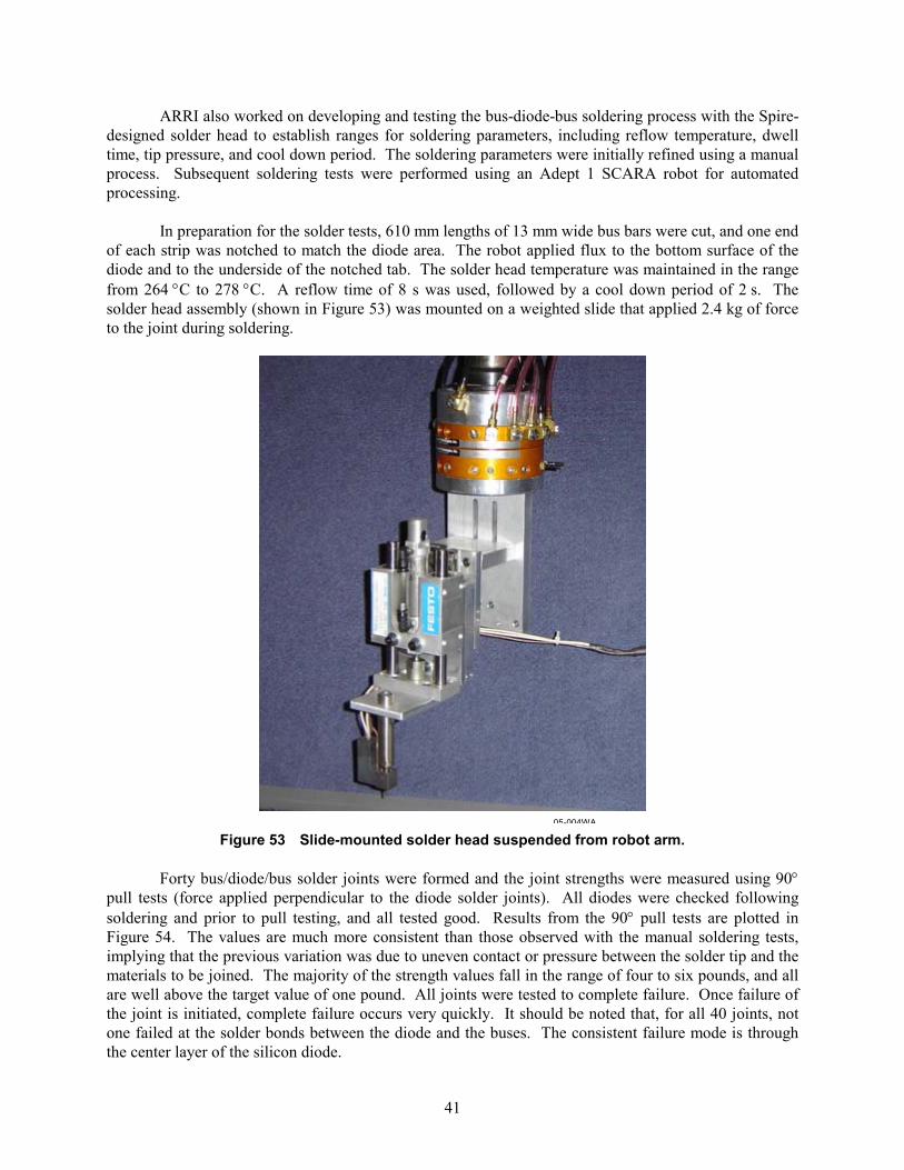
ARRI also worked on developing and testing the bus-diode-bus soldering process with the Spire-designed solder head to establish ranges for soldering parameters, including reflow temperature, dwell time, tip pressure, and cool down period. The soldering parameters were initially refined using a manual process. Subsequent soldering tests were performed using an Adept 1 SCARA robot for automated processing.
In preparation for the solder tests, 610 mm lengths of 13 mm wide bus bars were cut, and one end of each strip was notched to match the diode area. The robot applied flux to the bottom surface of the diode and to the underside of the notched tab. The solder head temperature was maintained in the range from 264 °C to 278 °C. A reflow time of 8 s was used, followed by a cool down period of 2 s. The solder head assembly (shown in Figure 53) was mounted on a weighted slide that applied 2.4 kg of force to the joint during soldering.
05-004WA
Figure 53 Slide-mounted solder head suspended from robot arm.
Forty bus/diode/bus solder joints were formed and the joint strengths were measured using 90° pull tests (force applied perpendicular to the diode solder joints). All diodes were checked following soldering and prior to pull testing, and all tested good. Results from the 90° pull tests are plotted in Figure 54. The values are much more consistent than those observed with the manual soldering tests, implying that the previous variation was due to uneven contact or pressure between the solder tip and the materials to be joined. The majority of the strength values fall in the range of four to six pounds, and all are well above the target value of one pound. All joints were tested to complete failure. Once failure of the joint is initiated, complete failure occurs very quickly. It should be noted that, for all 40 joints, not one failed at the solder bonds between the diode and the buses. The consistent failure mode is through the center layer of the silicon diode.
41
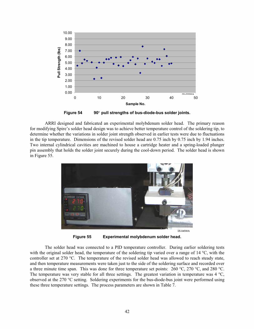
0.001.00
2.003.00
4.005.00
6.007.00
8.009.00
10.00
0 10 20 30 40
Sample No.
Pull
Stre
ngth
(lbs
)
50
05-005WA
Figure 54 90° pull strengths of bus-diode-bus solder joints.
ARRI designed and fabricated an experimental molybdenum solder head. The primary reason for modifying Spire’s solder head design was to achieve better temperature control of the soldering tip, to determine whether the variations in solder joint strength observed in earlier tests were due to fluctuations in the tip temperature. Dimensions of the revised solder head are 0.75 inch by 0.75 inch by 1.94 inches. Two internal cylindrical cavities are machined to house a cartridge heater and a spring-loaded plunger pin assembly that holds the solder joint securely during the cool-down period. The solder head is shown in Figure 55.
05-045WA
Figure 55 Experimental molybdenum solder head.
The solder head was connected to a PID temperature controller. During earlier soldering tests with the original solder head, the temperature of the soldering tip varied over a range of 14 °C, with the controller set at 270 °C. The temperature of the revised solder head was allowed to reach steady state, and then temperature measurements were taken just to the side of the soldering surface and recorded over a three minute time span. This was done for three temperature set points: 260 °C, 270 °C, and 280 °C. The temperature was very stable for all three settings. The greatest variation in temperature was 4 °C, observed at the 270 °C setting. Soldering experiments for the bus-diode-bus joint were performed using these three temperature settings. The process parameters are shown in Table 7.
42

Table 7 Process parameters for soldering bus-diode-bus joints.
Reflow Temp (°C)
Heat Force (kg)
Heat Time (s)
Cool Time (s)
Cool Force (kg)
260 2.4 8 5 0.23 270 2.4 5 5 0.23 280 2.4 5 5 0.23
Twenty solder joints were formed for each temperature setting and subjected to 90° pull tests to determine the joint strength and the failure mode. In 90% of the joints, failure occurred through the center of the diode, fracturing the bulk silicon. In the remaining 10% of the cases, the soldered interface between the diode and the bus bar failed. This type of failure had high strength, typically over 8 pounds. Pull strength data for joints made at 260°C, 270°C, and 280°C shows that, despite a more constant soldering tip temperature, the failure strength still varies considerably, between 1 and 11 lbs. Based on this information, it was concluded that the moderate temperature fluctuations (±7°C) of the original soldering head were not responsible for the variations in joint pull strengths. Since the lowest pull strengths occur when the silicon fractures, the variations may be due to stress in the diode caused by the difference in thermal expansion between the silicon diode and the copper bus bar.
Additional joints were soldered for the purpose of determining the shear strength of the bus-diode-bus joints. All joints were soldered at 270°C using the parameters in Table 7. Pull tests were done with the force applied parallel to the diode solder joints. Joints that failed at the soldered interface had shear strengths ranging from 25 to 44 lbs. In other tests, the copper bus bar failed before the solder joint sheared, with shear strengths in the range of 42-54 lbs. A plot of the shear strength values is shown in Figure 56. This data shows that the shear strength of the bus-diode-bus joints far exceeds the level required for modules.
05-050WA
Figure 56 Shear strength for bus-diode-bus solder joints. 3.3 Task 8 – Design Advanced Lamination Process Tool
We designed an advanced laminator for large area PV modules in this task. Given the size of our module (1.57 m x 3.68 m), we specified the lamination area at 2.00 m x 4.00 m. Initial design work focused on vacuum chamber structural design and heated platen design.
Solid models were created in CAD (SolidWorks) and a series of structural finite element analysis (FEA) simulations was done (with ANSYS) for various chamber plate thicknesses and reinforcing rib designs. Chamber deflection, stress, and factor of safety were calculated for each design. The load on the vacuum chamber is atmospheric pressure, set to 15 psi for these analyses. The resulting force on the chamber plates, which are 424 cm x 235 cm (167 inch x 92.5 inch), is 1,031 kN (231,700 lbf). Our design goals are to limit the total chamber deflection to 10 mm (0.39 inch) or less and to limit the stress on the chamber to obtain a factor of safety of 3 or more.
43
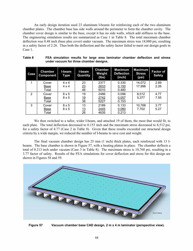
An early design iteration used 23 aluminum I-beams for reinforcing each of the two aluminum chamber plates. The chamber base has side walls around the perimeter to form the chamber cavity. The chamber cover design is similar to the base, except it has no side walls, which add stiffness to the base. The engineering simulation results are summarized as Case 1 in Table 8. The total maximum chamber deflection was 0.48 inch (base plus cover) under vacuum. The maximum stress was 18,000 psi, resulting in a safety factor of 2.26. Thus both the deflection and the safety factor failed to meet our design goals in Case 1. Table 8 FEA simulation results for large area laminator chamber deflection and stress
under vacuum for three chamber designs.
Case Chamber
Component I-beam Type
I-beam Quantity
Chamber Weight
(lbs)
Maximum Deflection
(inch)
Maximum Stress (psi)
Factor of Safety
1 Cover Base Total
4 x 4 4 x 4
23 23 46
2377 2633 5010
0.330 0.150 0.480
14,072 17,998
2.89 2.26
2 Cover
Base Total
8 x 5 8 x 5
19 19 38
2486 2742 5227
0.096 0.057 0.153
8,512 5,377
4.77 7.55
3 Cover
Base Total
8 x 5 8 x 5
13 13 26
2189 2445 4635
0.133 0.080 0.213
10,768 7,702
3.77 5.27
We then switched to a taller, wider I-beam, and attached 19 of them, the most that would fit, to each plate. The total deflection decreased to 0.153 inch and the maximum stress decreased to 8,512 psi, for a safety factor of 4.77 (Case 2 in Table 8). Given that these results exceeded our structural design criteria by a wide margin, we reduced the number of I-beams to save cost and weight.
The final vacuum chamber design has 25 mm (1 inch) thick plates, each reinforced with 13 I-beams. The base chamber is shown in Figure 57, with a heating platen in place. The chamber deflects a total of 0.213 inch under vacuum (Case 3 in Table 8). The maximum stress is 10,768 psi, resulting in a 3.77 factor of safety. Results of the FEA simulations for cover deflection and stress for this design are shown in Figures 58 and 59.
05-013WA
Figure 57 Vacuum chamber base CAD design, 2 m x 4 m laminator (perspective view).
44
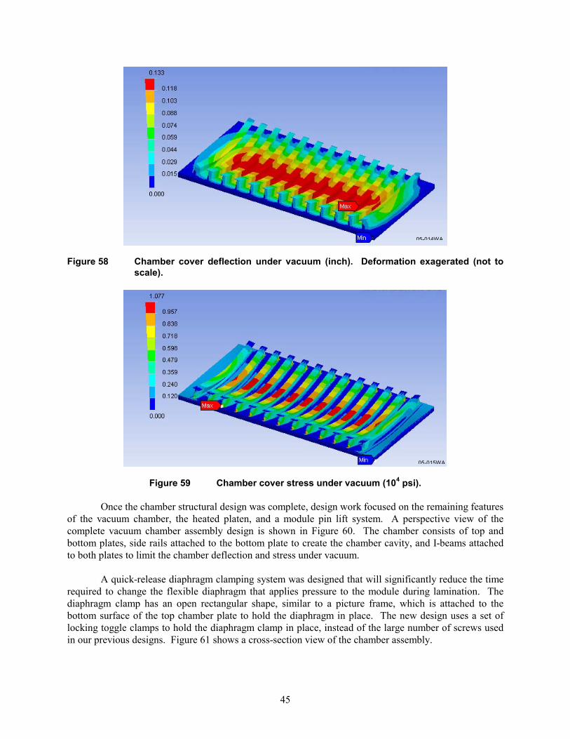
05-014WA
Figure 58 Chamber cover deflection under vacuum (inch). Deformation exagerated (not to
scale).
05-015WA
Figure 59 Chamber cover stress under vacuum (104 psi).
Once the chamber structural design was complete, design work focused on the remaining features
of the vacuum chamber, the heated platen, and a module pin lift system. A perspective view of the complete vacuum chamber assembly design is shown in Figure 60. The chamber consists of top and bottom plates, side rails attached to the bottom plate to create the chamber cavity, and I-beams attached to both plates to limit the chamber deflection and stress under vacuum.
A quick-release diaphragm clamping system was designed that will significantly reduce the time required to change the flexible diaphragm that applies pressure to the module during lamination. The diaphragm clamp has an open rectangular shape, similar to a picture frame, which is attached to the bottom surface of the top chamber plate to hold the diaphragm in place. The new design uses a set of locking toggle clamps to hold the diaphragm clamp in place, instead of the large number of screws used in our previous designs. Figure 61 shows a cross-section view of the chamber assembly.
45

05-023WA
Figure 60 Large area laminator vacuum chamber design.
05-024WA
Figure 61 Laminator vacuum chamber design, cross-section view.
A module pin lift design was completed for the large laminator. The pin lift is important to
prevent large modules from curling when placed on a heated platen. Curling occurs because the surface of the glass in contact with the platen is hotter than the opposite surface of the glass, and therefore longer due to thermal expansion. The pins hold the glass slightly above the surface of the platen during the initial evacuation step in the lamination process. The pin lift system uses sliding cam bars under the heated platen to push pins, located in holes in the platen, from a position slightly below the surface of the platen to a height of up to 5 mm above the platen. The pin up height is adjustable, with a nominal 3 mm height recommended for production.
46
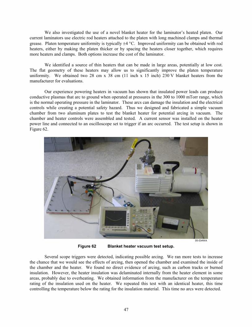
We also investigated the use of a novel blanket heater for the laminator’s heated platen. Our current laminators use electric rod heaters attached to the platen with long machined clamps and thermal grease. Platen temperature uniformity is typically ±4 °C. Improved uniformity can be obtained with rod heaters, either by making the platen thicker or by spacing the heaters closer together, which requires more heaters and clamps. Both options increase the cost of the laminator.
We identified a source of thin heaters that can be made in large areas, potentially at low cost. The flat geometry of these heaters may allow us to significantly improve the platen temperature uniformity. We obtained two 28 cm x 38 cm (11 inch x 15 inch) 230 V blanket heaters from the manufacturer for evaluations.
Our experience powering heaters in vacuum has shown that insulated power leads can produce conductive plasmas that arc to ground when operated at pressures in the 300 to 1000 mTorr range, which is the normal operating pressure in the laminator. These arcs can damage the insulation and the electrical controls while creating a potential safety hazard. Thus we designed and fabricated a simple vacuum chamber from two aluminum plates to test the blanket heater for potential arcing in vacuum. The chamber and heater controls were assembled and tested. A current sensor was installed on the heater power line and connected to an oscilloscope set to trigger if an arc occurred. The test setup is shown in Figure 62.
05-034WA
Figure 62 Blanket heater vacuum test setup.
Several scope triggers were detected, indicating possible arcing. We ran more tests to increase the chance that we would see the effects of arcing, then opened the chamber and examined the inside of the chamber and the heater. We found no direct evidence of arcing, such as carbon tracks or burned insulation. However, the heater insulation was delaminated internally from the heater element in some areas, probably due to overheating. We obtained information from the manufacturer on the temperature rating of the insulation used on the heater. We repeated this test with an identical heater, this time controlling the temperature below the rating for the insulation material. This time no arcs were detected.
47

3.4 Task 9 – Design Lamination Automation Mechanical design work was completed for an automated conveyor system for transporting
modules through the large area laminator (2 m x 4 m module size capacity). The design is shown in Figure 63. The drive components for the conveyor were sized and selected. Mechanical design models for the drive conveyor and a conveyor cleaning brush were created. Detail design drawings and assembly drawings were generated from the models.
05-096WA
Figure 63 Laminator automation design.
The conveyor belt is fabricated from a Teflon2-coated fiberglass material, similar to the release
sheets we use to keep EVA encapsulant from sticking to the interior surfaces of the laminator. A motor-driven cylindrical brush is included to remove any EVA or other material that may accumulate on the belt.
A view of the CAD model of the conveyor drive design is shown in Figure 64. The laminator vacuum chamber will sit inside the drive system, with the heated platen and top of the chamber side walls coplanar with the conveyor belt. Belt travel is left to right in Figure 64.
05-026WA
Figure 64 Module conveyor drive design for laminator automation (conveyor belt and
laminator not shown for clarity).
48

3.5 Task 10 – Design Large Area Solar Simulator Spire currently produces upward flashing solar simulators that can test modules up to 1.37 m x
2.00 m. In Task 10 we designed a simulator with a significantly larger 2.0 m x 4.0 m test area for the Brightfield module. We maintained the flash up geometry for the larger simulator, since it simplifies product handling by allowing modules to be transported over the simulator on a conveyor.
A view of the solid CAD model of the simulator is shown in Figure 65. The simulator has four 2.0 m long xenon lamps positioned side-by-side under the test plane. Adjustable reflecting surfaces direct light to the test plane, while optical filters correct the spectrum to Air Mass 1.5 Global, per ASTM E927-053 and IEC 60904-9.4 A pair of motor-driven belt conveyors supports the module at its edges and transports it through the simulator. The conveyor positions are adjustable to suit the module width.
05-097WA
Figure 65 Large area solar simulator design with 2 m x 4 m test plane. Side panels not
shown for clarity. 3.5.1 Single-Flash Long Pulse Xenon Light Source
We developed a single-flash, long pulse xenon light source for solar simulators. Our standard simulator uses multiple (50 to 200) short pulses (1 ms per pulse at 7 to 10 Hz) for each module I-V curve. A single flash approach, in which an I-V curve is measured during a single lamp flash, shortens the test time from ~20 s to less than 1 s per module. A longer pulse, on the order of 100 ms, allows the simulator to be used for solar cells with slow response times, such as SunPower’s high efficiency back contact cells, Sanyo’s Heterojunction with Intrinsic Thin Layer (HIT) cells, and some types of thin film cells made from CIS, CdTe, or a-Si.
We successfully developed a unique active feedback lamp control system that uses power semiconductors (MOSFETs) to control the flash profile of a xenon lamp. This lamp control method allows us to build a long pulse, single flash simulator without a large number of big, heavy, and expensive inductors.
49

We designed, assembled, and tested a prototype lamp regulator printed circuit board (Spire no. 909-0401), shown in Figure 66. The board controls a bank of high voltage power MOSFETs in response to an applied reference signal. Initial checkout involved applying signals to the board from a function generator and observing the behavior of the board. Changes were made to some board components as a result of these tests.
Figure 66 Spire lamp regulator circuit board for a single-flash long-pulse solar simulator. 05-058WA
Work then began on discharging a large capacitor (2400 μF, 3600 VDC) with a regulated current,
in preparation for a controlled flash of a xenon arc lamp. An electrical panel was assembled, including the Spire lamp regulator board, four power MOSFETs, and several high voltage relays and power resistors, which provide backup discharge capability.
The capacitor was first discharged through a 180 Ω power resistor network. This was successful up to the point where MOSFET failures occurred, due to transient over-voltage during turn-on. We then substituted a 1955 mm long xenon arc lamp in place of the resistor network, since its terminal voltage is effectively independent of current. The lamp flashed successfully at a constant current set point of 6.3 A. Two additional MOSFETs were installed on the panel, and lamp current was increased in steps up to 16 A, at an operating voltage of 2350 V. The pulse width under these conditions was about 65 milliseconds at constant current.
A reference cell was then installed and used as the feedback source for the light pulse, which is our actual lamp control scheme. This circuit produced flashes with very uniform light intensity for 66 ms. The light pulse had an initial spike followed by a long flat region, which ends when the capacitor is discharged to the point where it can no longer provide sufficient current to the lamp. We then increased the pulse length by adding more capacitance to the circuit. Figure 67 shows a 78 ms flat light pulse generated by a 1.955 m long xenon lamp with 3600 μF capacitance. The lamp current was 24 A during the flash, sufficient to produce 1 sun (100 mW/cm2) of light intensity in a solar simulator.
50
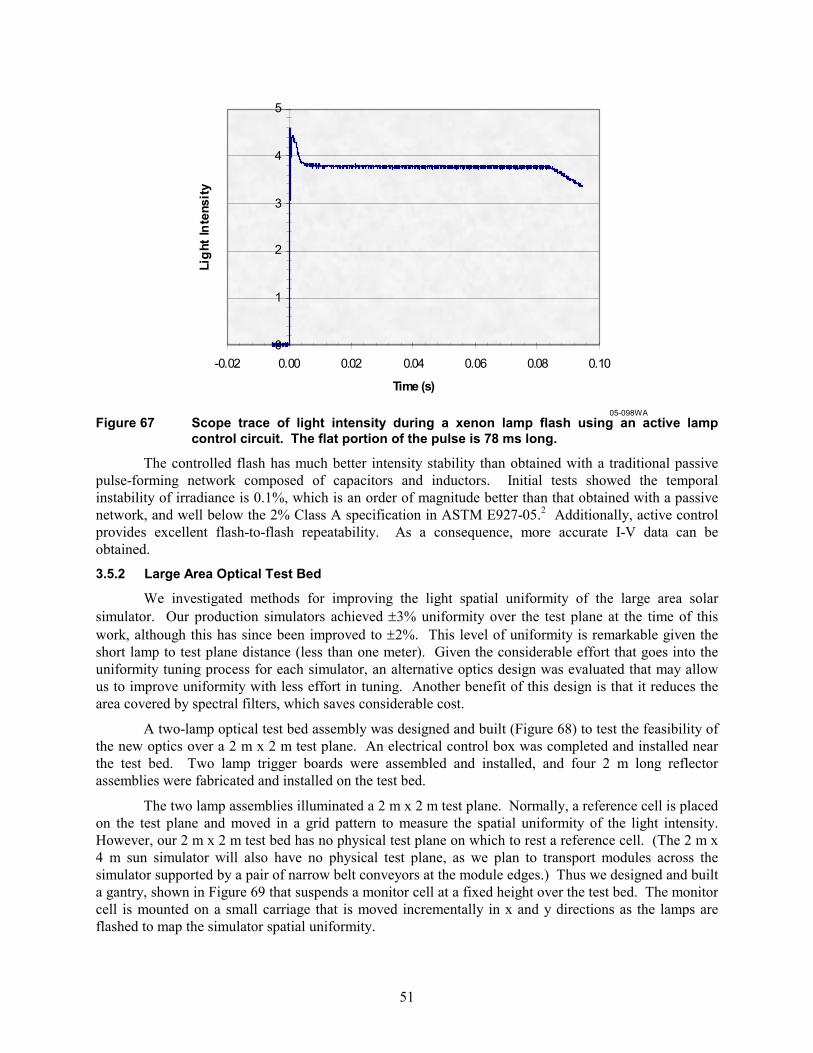
0
1
2
3
4
5
-0.02 0.00 0.02 0.04 0.06 0.08 0.10
Time (s)
Ligh
t Int
ensi
ty
Figure 67 Scope trace of light intensity during a xenon lamp flash using an active lamp
control circuit. The flat portion of the pulse is 78 ms long.
05-098WA
The controlled flash has much better intensity stability than obtained with a traditional passive pulse-forming network composed of capacitors and inductors. Initial tests showed the temporal instability of irradiance is 0.1%, which is an order of magnitude better than that obtained with a passive network, and well below the 2% Class A specification in ASTM E927-05.2 Additionally, active control provides excellent flash-to-flash repeatability. As a consequence, more accurate I-V data can be obtained.
3.5.2 Large Area Optical Test Bed
We investigated methods for improving the light spatial uniformity of the large area solar simulator. Our production simulators achieved ±3% uniformity over the test plane at the time of this work, although this has since been improved to ±2%. This level of uniformity is remarkable given the short lamp to test plane distance (less than one meter). Given the considerable effort that goes into the uniformity tuning process for each simulator, an alternative optics design was evaluated that may allow us to improve uniformity with less effort in tuning. Another benefit of this design is that it reduces the area covered by spectral filters, which saves considerable cost.
A two-lamp optical test bed assembly was designed and built (Figure 68) to test the feasibility of the new optics over a 2 m x 2 m test plane. An electrical control box was completed and installed near the test bed. Two lamp trigger boards were assembled and installed, and four 2 m long reflector assemblies were fabricated and installed on the test bed.
The two lamp assemblies illuminated a 2 m x 2 m test plane. Normally, a reference cell is placed on the test plane and moved in a grid pattern to measure the spatial uniformity of the light intensity. However, our 2 m x 2 m test bed has no physical test plane on which to rest a reference cell. (The 2 m x 4 m sun simulator will also have no physical test plane, as we plan to transport modules across the simulator supported by a pair of narrow belt conveyors at the module edges.) Thus we designed and built a gantry, shown in Figure 69 that suspends a monitor cell at a fixed height over the test bed. The monitor cell is mounted on a small carriage that is moved incrementally in x and y directions as the lamps are flashed to map the simulator spatial uniformity.
51
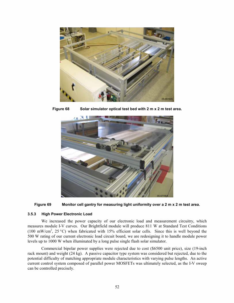
05-051WA
Figure 68 Solar simulator optical test bed with 2 m x 2 m test area.
05-071WA
Figure 69 Monitor cell gantry for measuring light uniformity over a 2 m x 2 m test area.
3.5.3 High Power Electronic Load
We increased the power capacity of our electronic load and measurement circuitry, which measures module I-V curves. Our Brightfield module will produce 811 W at Standard Test Conditions (100 mW/cm2, 25 °C) when fabricated with 15% efficient solar cells. Since this is well beyond the 500 W rating of our current electronic load circuit board, we are redesigning it to handle module power levels up to 1000 W when illuminated by a long pulse single flash solar simulator.
Commercial bipolar power supplies were rejected due to cost ($6500 unit price), size (19-inch rack mount) and weight (24 kg). A passive capacitor type system was considered but rejected, due to the potential difficulty of matching appropriate module characteristics with varying pulse lengths. An active current control system composed of parallel power MOSFETs was ultimately selected, as the I-V sweep can be controlled precisely.
52
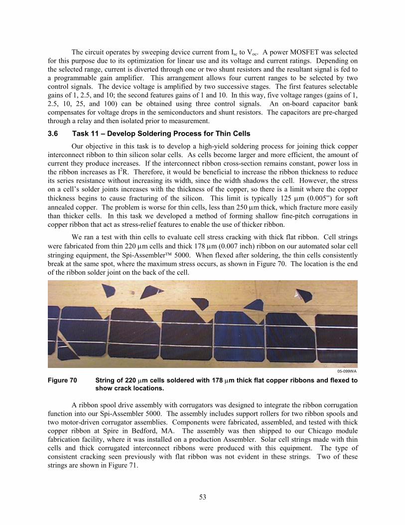
The circuit operates by sweeping device current from Isc to Voc. A power MOSFET was selected for this purpose due to its optimization for linear use and its voltage and current ratings. Depending on the selected range, current is diverted through one or two shunt resistors and the resultant signal is fed to a programmable gain amplifier. This arrangement allows four current ranges to be selected by two control signals. The device voltage is amplified by two successive stages. The first features selectable gains of 1, 2.5, and 10; the second features gains of 1 and 10. In this way, five voltage ranges (gains of 1, 2.5, 10, 25, and 100) can be obtained using three control signals. An on-board capacitor bank compensates for voltage drops in the semiconductors and shunt resistors. The capacitors are pre-charged through a relay and then isolated prior to measurement.
3.6 Task 11 – Develop Soldering Process for Thin Cells Our objective in this task is to develop a high-yield soldering process for joining thick copper
interconnect ribbon to thin silicon solar cells. As cells become larger and more efficient, the amount of current they produce increases. If the interconnect ribbon cross-section remains constant, power loss in the ribbon increases as I2R. Therefore, it would be beneficial to increase the ribbon thickness to reduce its series resistance without increasing its width, since the width shadows the cell. However, the stress on a cell’s solder joints increases with the thickness of the copper, so there is a limit where the copper thickness begins to cause fracturing of the silicon. This limit is typically 125 μm (0.005”) for soft annealed copper. The problem is worse for thin cells, less than 250 μm thick, which fracture more easily than thicker cells. In this task we developed a method of forming shallow fine-pitch corrugations in copper ribbon that act as stress-relief features to enable the use of thicker ribbon.
We ran a test with thin cells to evaluate cell stress cracking with thick flat ribbon. Cell strings were fabricated from thin 220 μm cells and thick 178 μm (0.007 inch) ribbon on our automated solar cell stringing equipment, the Spi-Assembler™ 5000. When flexed after soldering, the thin cells consistently break at the same spot, where the maximum stress occurs, as shown in Figure 70. The location is the end of the ribbon solder joint on the back of the cell.
05-099WA
Figure 70 String of 220 μm cells soldered with 178 μm thick flat copper ribbons and flexed to show crack locations.
A ribbon spool drive assembly with corrugators was designed to integrate the ribbon corrugation
function into our Spi-Assembler 5000. The assembly includes support rollers for two ribbon spools and two motor-driven corrugator assemblies. Components were fabricated, assembled, and tested with thick copper ribbon at Spire in Bedford, MA. The assembly was then shipped to our Chicago module fabrication facility, where it was installed on a production Assembler. Solar cell strings made with thin cells and thick corrugated interconnect ribbons were produced with this equipment. The type of consistent cracking seen previously with flat ribbon was not evident in these strings. Two of these strings are shown in Figure 71.
53
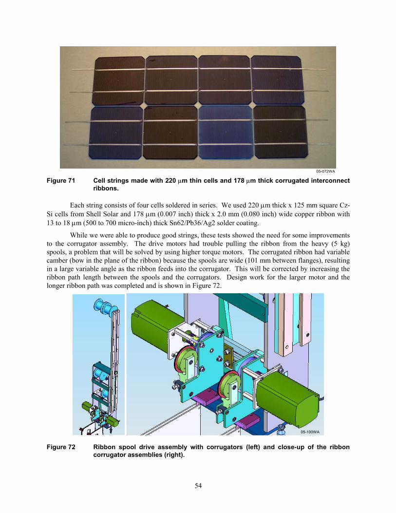
05-072WA
Figure 71 Cell strings made with 220 μm thin cells and 178 μm thick corrugated interconnect ribbons.
Each string consists of four cells soldered in series. We used 220 μm thick x 125 mm square Cz-
Si cells from Shell Solar and 178 μm (0.007 inch) thick x 2.0 mm (0.080 inch) wide copper ribbon with 13 to 18 μm (500 to 700 micro-inch) thick Sn62/Pb36/Ag2 solder coating.
While we were able to produce good strings, these tests showed the need for some improvements to the corrugator assembly. The drive motors had trouble pulling the ribbon from the heavy (5 kg) spools, a problem that will be solved by using higher torque motors. The corrugated ribbon had variable camber (bow in the plane of the ribbon) because the spools are wide (101 mm between flanges), resulting in a large variable angle as the ribbon feeds into the corrugator. This will be corrected by increasing the ribbon path length between the spools and the corrugators. Design work for the larger motor and the longer ribbon path was completed and is shown in Figure 72.
05-100WA
Figure 72 Ribbon spool drive assembly with corrugators (left) and close-up of the ribbon
corrugator assemblies (right).
54

4 PHASE 3 TECHNICAL DISCUSSION
4.1 Task 14 – Fabricate and Test Large Area Simulator Spire currently produces upward flashing solar simulators that can test modules with active areas
up to 1.4 m x 2.0 m. In this task we fabricated and tested a simulator with a significantly larger test area, required for Spire’s 1.6 m x 3.8 m Brightfield module design. We use a flash-up geometry for the large simulator, since it simplifies product handling by allowing modules to be transported over the simulator on a conveyor. This system is designated the Spi-Sun Simulator 2040SLP, where 2040 refers to the nominal test plane area (2.0 m x 4.0 m) and SLP stands for Single Long Pulse, the advanced lamp control scheme developed in this program. The design used for the large area solar simulator is based on development work done on an optical test bed and on our long-pulse xenon lamp electronics in Task 10. Key design elements follow:
• The simulator uses four 1.955 m long xenon lamps to illuminate a 2.0 m x 4.0 m test area.
• A mirror approach is used for light distribution, as opposed to the diffuse reflector method used in our current commercial simulators.
• A row of spectral filters is mounted over each mirror, resulting in a reduction of filter area by approximately 50% compared to our standard simulators.
• Baffles for trimming uniformity work by blocking, not absorbing, light, to avoid potential spectrum modifications.
• Acrylic sheets cover the spectral filters to protect them from damage from falling objects, since the simulator has no top cover glass.
• Reference cells are mounted at the test plane height, along the centerline of each lamp, at the edge of the 2 m wide test plane. The reference cells provide closed-loop lamp intensity control.
• We incorporated our new quick-release lamp mounting blocks for ease of servicing and reduced lamp breakage.
• Support rails were provided in the 4 m direction to support modules or a uniformity cell at the test plane for characterizing spatial uniformity. Powered edge conveyors can be used in place of the rails to automate this function.
4.1.1 Final Design, Fabrication, and Assembly of a Large Area Simulator
We developed a new mechanical design for our xenon lamp mounting assembly. The new design simplifies the components to reduce cost while allowing for easier and faster lamp changes, with less stress on the lamps. Each end of a 1.955 m long xenon lamp is supported in a contact block housing. The top half of the housing is attached to the base with a pair of latches that allow it to be removed easily, without tools. Views from the 3-D CAD model are shown in Figure 73. Drawings were released and the components for four lamp mount assemblies were fabricated, assembled, and tested.
A large spectral filter mount assembly was designed and fabricated for the 2 m x 4 m simulator. The assembly uses approximately half the filter area for a given test plane area than our current commercial solar simulators, which reduces cost. The assembly includes the spectral filters, filter hangars, filter covers, and retainers. The retainers are attached with screws that require a tool to remove the filter covers, as a safety feature to prevent access to high voltage on the lamps below the filters.
55
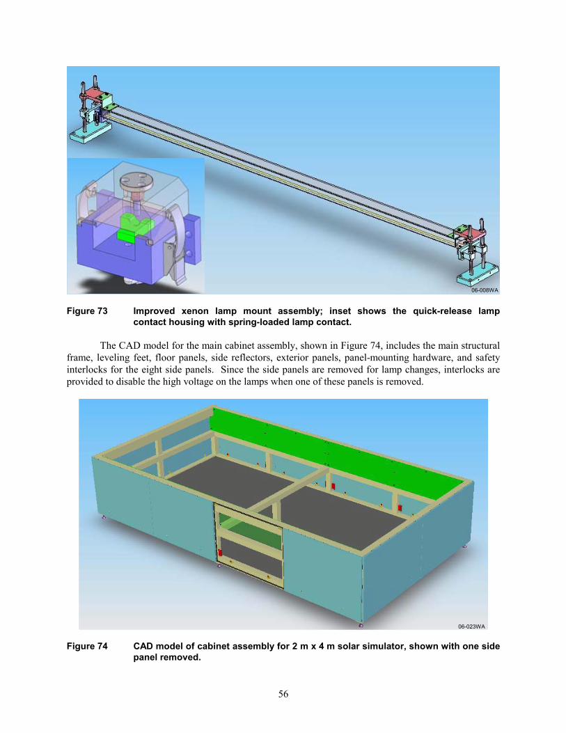
06-008WA
Figure 73 Improved xenon lamp mount assembly; inset shows the quick-release lamp
contact housing with spring-loaded lamp contact. The CAD model for the main cabinet assembly, shown in Figure 74, includes the main structural frame, leveling feet, floor panels, side reflectors, exterior panels, panel-mounting hardware, and safety interlocks for the eight side panels. Since the side panels are removed for lamp changes, interlocks are provided to disable the high voltage on the lamps when one of these panels is removed.
06-023WA
Figure 74 CAD model of cabinet assembly for 2 m x 4 m solar simulator, shown with one side
panel removed.
56

Mechanical design work was completed for the electrical controls cabinet for the 2040 SLP simulator. The controls reside in a 108 inch wide x 16 inch deep x 42 inch high four-door enclosure. The enclosure includes components for the lamp power supplies and the module measurement electronics. The locations of the electrical components were laid out and a 3D CAD model was created in SolidWorks. A view from the model is shown in Figure 75. Detail drawings were produced for the cabinet interior panels on which the components are mounted, and for modifications (cut-outs and holes) to the cabinet’s exterior surfaces. A swing arm for mounting a panel PC (combination PC with flat screen monitor) and a keyboard is attached to the left side of the cabinet.
07-006WA
Figure 75 CAD model of the electrical controls cabinet for the Spi-Sun Simulator 2040 SLP.
A major simulator design improvement developed in this program is the use of a single long (up
to 100 ms) light pulse for each IV curve measurement. Active flash lamp control was developed to allow the simulator to produce long pulses of virtually constant intensity. A reference cell is used as the feedback source for the light pulse.
Artwork files were produced for three new circuit boards for the long-pulse simulator:
• 912-0200 PCB, LOAD AND MEASUREMENT BOARD, SINGLE FLASH – this is the main circuitry used for module IV curve measurements.
• 913-0200 PCB, DT INTERFACE – this is a small passive breakout board that adapts the data acquisition board to the Load and Measurement Board and multiple (one to four) Lamp Control boards, one for each lamp in a simulator.
• 909-0200 LAMP CONTROL PCB, SINGLE FLASH – this board is used for active control of a single xenon lamp. Artwork modifications were made to support design changes identified during testing of the first prototype.
57
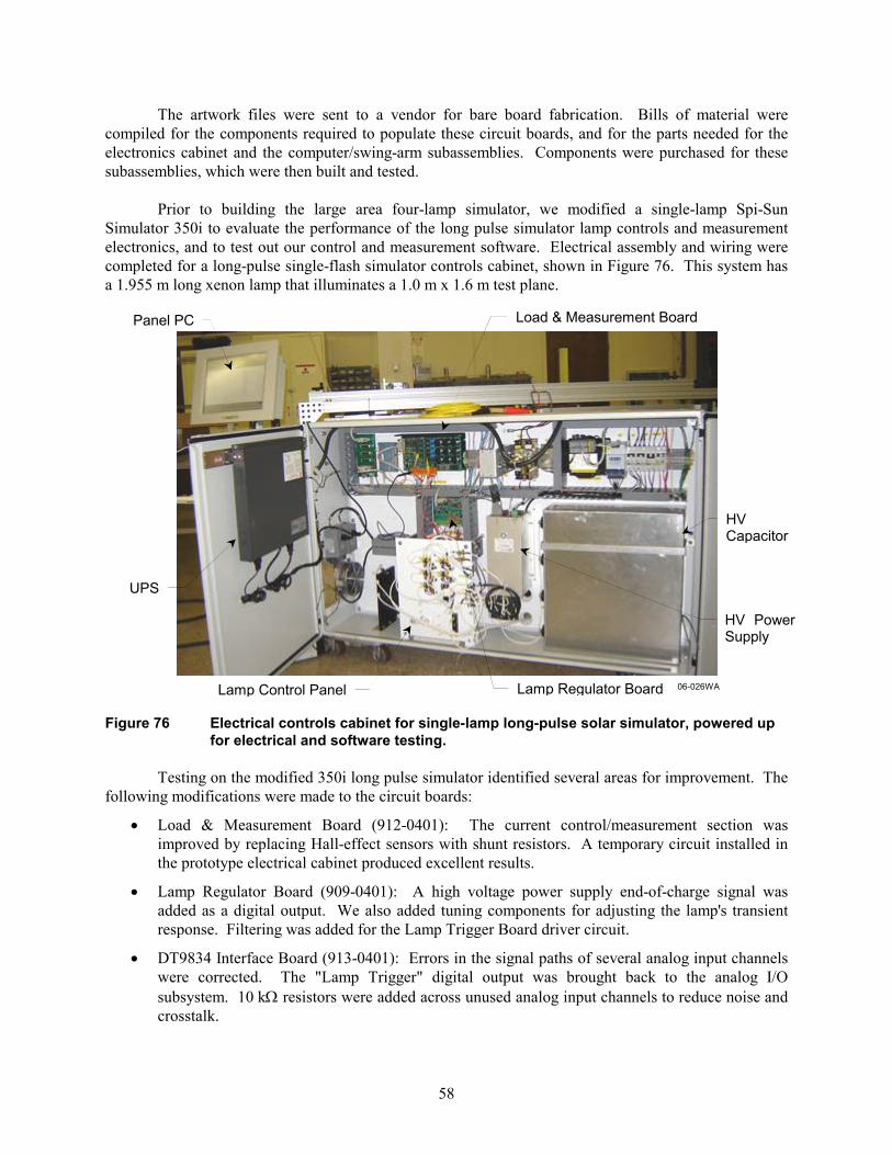
The artwork files were sent to a vendor for bare board fabrication. Bills of material were compiled for the components required to populate these circuit boards, and for the parts needed for the electronics cabinet and the computer/swing-arm subassemblies. Components were purchased for these subassemblies, which were then built and tested.
Prior to building the large area four-lamp simulator, we modified a single-lamp Spi-Sun Simulator 350i to evaluate the performance of the long pulse simulator lamp controls and measurement electronics, and to test out our control and measurement software. Electrical assembly and wiring were completed for a long-pulse single-flash simulator controls cabinet, shown in Figure 76. This system has a 1.955 m long xenon lamp that illuminates a 1.0 m x 1.6 m test plane.
Load & Measurement Board Panel PC
HV Capacitor
UPS
HV Power Supply
Lamp Regulator Board Lamp Control Panel 06-026WA
Figure 76 Electrical controls cabinet for single-lamp long-pulse solar simulator, powered up
for electrical and software testing.
Testing on the modified 350i long pulse simulator identified several areas for improvement. The following modifications were made to the circuit boards:
• Load & Measurement Board (912-0401): The current control/measurement section was improved by replacing Hall-effect sensors with shunt resistors. A temporary circuit installed in the prototype electrical cabinet produced excellent results.
• Lamp Regulator Board (909-0401): A high voltage power supply end-of-charge signal was added as a digital output. We also added tuning components for adjusting the lamp's transient response. Filtering was added for the Lamp Trigger Board driver circuit.
• DT9834 Interface Board (913-0401): Errors in the signal paths of several analog input channels were corrected. The "Lamp Trigger" digital output was brought back to the analog I/O subsystem. 10 kΩ resistors were added across unused analog input channels to reduce noise and crosstalk.
58
Software development for the new simulator controls included the following activities:
• VisualBasic code was written to control a commercial data acquisition board. Testing confirmed the control of digital and analog outputs, and confirmed measurements made by digital and analog inputs.
• Code was written to read in module and reference cell temperatures via a USB thermocouple input module.
• New parameters (user selectable settings) were added that are specific to the long pulse simulator.
• VisualBasic code was written to control the lamp flash, control the electronic load, and measure an IV curve. The I-V test sequence code was tested and validated.
• Dual lamp control software was completed to provide active long-pulse lamp control for two lamps flashing simultaneously. This control approach is used in our commercial Spi-Sun Simulator 4600SLP, a long pulse simulator with two xenon lamps and a 1.4 m x 2 m test area.
• Tests showed that software-triggered data acquisition was not reliable, so we wired in a trigger signal to the D/A card external trigger input from the lamp trigger output. All analog data acquisition during an I-V curve sweep is now triggered by this signal. The hardware trigger produced excellent results.
• When electronic load sweep times are long enough to measure a large number of I-V data points (~900) per I-V curve, we found that it is not necessary to do a curve fit around the Pmax point to determine Pmax, Vmp, and Imp. We can simply choose the greatest V × I value. Repeatability (standard deviation ÷ average) using this method is typically 0.1%. Using a cubic curve fit method near Pmax we obtained repeatability >0.2%.
• Repeatability for the Pmax measurement begins to suffer for shorter sweep times, when the number of data points drops below 400 points per curve, so curve fitting is used when the number of data points is less than 400. We implemented a new 6th order polynomial function for the load voltage output waveform for the electronic load. This replaced a three-part (linear fit near Isc, cubic fit near Pmax, linear fit near Voc) waveform used previously. The new waveform produces a more consistent data point distribution throughout the IV curve. A steep ramp at the beginning of the waveform forces the module voltage ≤ 0 V for reliable Isc measurements. The new waveform also allows the electronic load to handle a wider range of module currents without adjusting setup parameters.
• We added an "end of charge" digital input from the high voltage power supply that charges the xenon lamp capacitors. This feature is used to signal when capacitor charging is complete and the xenon lamp is ready to flash.
We developed a new simulator function for measuring two IV curves at two light intensities in a
single flash. This technique is useful for making accurate module series resistance (Rs) measurements, using the method defined in IEC standard 60891.5 In practice, we flash the lamp at a starting intensity (usually 100 mW/cm2), then ramp the lamp intensity down to a reduced irradiance (as low as 70 mW/cm2) during the same light pulse. Since the lamp control is closed loop, this is relatively simple to do. The amount of time at each intensity is roughly half the total programmed sweep length. The electronic load sweeps two separate IV curves during the pulse, one at each intensity.
59
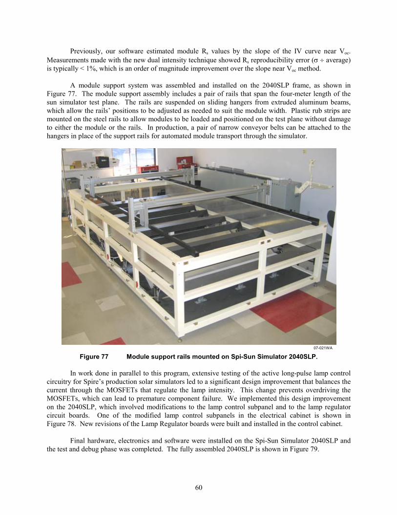
Previously, our software estimated module Rs values by the slope of the IV curve near Voc. Measurements made with the new dual intensity technique showed Rs reproducibility error (σ ÷ average) is typically < 1%, which is an order of magnitude improvement over the slope near Voc method.
A module support system was assembled and installed on the 2040SLP frame, as shown in Figure 77. The module support assembly includes a pair of rails that span the four-meter length of the sun simulator test plane. The rails are suspended on sliding hangers from extruded aluminum beams, which allow the rails’ positions to be adjusted as needed to suit the module width. Plastic rub strips are mounted on the steel rails to allow modules to be loaded and positioned on the test plane without damage to either the module or the rails. In production, a pair of narrow conveyor belts can be attached to the hangers in place of the support rails for automated module transport through the simulator.
07-021WA
Figure 77 Module support rails mounted on Spi-Sun Simulator 2040SLP. In work done in parallel to this program, extensive testing of the active long-pulse lamp control
circuitry for Spire’s production solar simulators led to a significant design improvement that balances the current through the MOSFETs that regulate the lamp intensity. This change prevents overdriving the MOSFETs, which can lead to premature component failure. We implemented this design improvement on the 2040SLP, which involved modifications to the lamp control subpanel and to the lamp regulator circuit boards. One of the modified lamp control subpanels in the electrical cabinet is shown in Figure 78. New revisions of the Lamp Regulator boards were built and installed in the control cabinet.
Final hardware, electronics and software were installed on the Spi-Sun Simulator 2040SLP and the test and debug phase was completed. The fully assembled 2040SLP is shown in Figure 79.
60
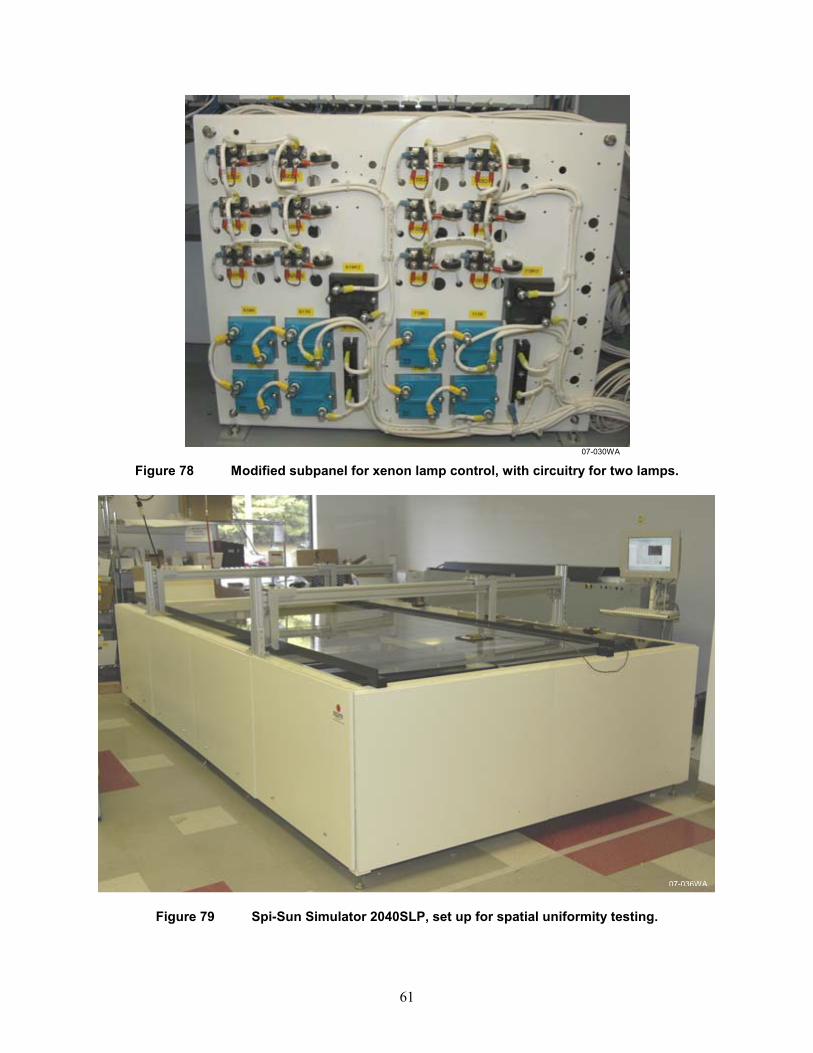
07-030WA
Figure 78 Modified subpanel for xenon lamp control, with circuitry for two lamps.
07-036WA
Figure 79 Spi-Sun Simulator 2040SLP, set up for spatial uniformity testing.
61
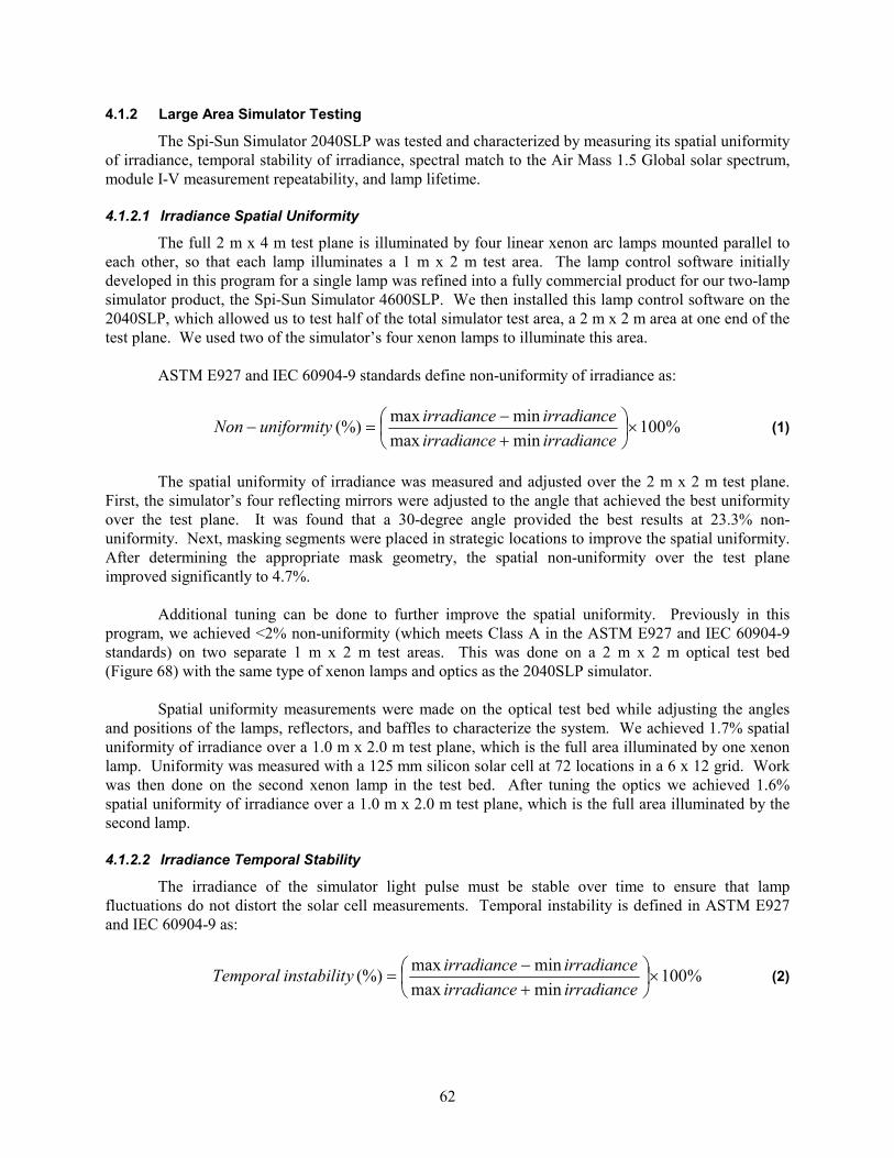
4.1.2 Large Area Simulator Testing
The Spi-Sun Simulator 2040SLP was tested and characterized by measuring its spatial uniformity of irradiance, temporal stability of irradiance, spectral match to the Air Mass 1.5 Global solar spectrum, module I-V measurement repeatability, and lamp lifetime. 4.1.2.1 Irradiance Spatial Uniformity
The full 2 m x 4 m test plane is illuminated by four linear xenon arc lamps mounted parallel to each other, so that each lamp illuminates a 1 m x 2 m test area. The lamp control software initially developed in this program for a single lamp was refined into a fully commercial product for our two-lamp simulator product, the Spi-Sun Simulator 4600SLP. We then installed this lamp control software on the 2040SLP, which allowed us to test half of the total simulator test area, a 2 m x 2 m area at one end of the test plane. We used two of the simulator’s four xenon lamps to illuminate this area.
ASTM E927 and IEC 60904-9 standards define non-uniformity of irradiance as:
%100minmaxminmax(%) ×⎟
⎠⎞
⎜⎝⎛
+−
=−irradianceirradianceirradianceirradianceuniformityNon (1)
The spatial uniformity of irradiance was measured and adjusted over the 2 m x 2 m test plane.
First, the simulator’s four reflecting mirrors were adjusted to the angle that achieved the best uniformity over the test plane. It was found that a 30-degree angle provided the best results at 23.3% non-uniformity. Next, masking segments were placed in strategic locations to improve the spatial uniformity. After determining the appropriate mask geometry, the spatial non-uniformity over the test plane improved significantly to 4.7%.
Additional tuning can be done to further improve the spatial uniformity. Previously in this program, we achieved <2% non-uniformity (which meets Class A in the ASTM E927 and IEC 60904-9 standards) on two separate 1 m x 2 m test areas. This was done on a 2 m x 2 m optical test bed (Figure 68) with the same type of xenon lamps and optics as the 2040SLP simulator.
Spatial uniformity measurements were made on the optical test bed while adjusting the angles and positions of the lamps, reflectors, and baffles to characterize the system. We achieved 1.7% spatial uniformity of irradiance over a 1.0 m x 2.0 m test plane, which is the full area illuminated by one xenon lamp. Uniformity was measured with a 125 mm silicon solar cell at 72 locations in a 6 x 12 grid. Work was then done on the second xenon lamp in the test bed. After tuning the optics we achieved 1.6% spatial uniformity of irradiance over a 1.0 m x 2.0 m test plane, which is the full area illuminated by the second lamp. 4.1.2.2 Irradiance Temporal Stability
The irradiance of the simulator light pulse must be stable over time to ensure that lamp fluctuations do not distort the solar cell measurements. Temporal instability is defined in ASTM E927 and IEC 60904-9 as:
%100minmaxminmax(%) ×⎟
⎠⎞
⎜⎝⎛
+−
=irradianceirradianceirradianceirradianceyinstabilitTemporal (2)
62
The 2040 SLP lamp control circuitry has an independent active intensity feedback loop for each xenon lamp. The light pulse irradiance was measured over a 50 ms period and the temporal instability was found to be 0.11% for both lamps, as shown in Table 9. This value meets the Class A requirements for both ASTM E927 and IEC 60904-9, which specify a temporal instability of ≤2%.
Table 9 Irradiance temporal instability for two xenon lamps in the 2040SLP simulator.
Lamp 1 Lamp 2 Max irradiance: 5.489 5.618 Min irradiance: 5.477 5.606 Temporal instability: 0.11% 0.11%
A plot of lamp intensity vs. time is shown in Figure 80. In this figure, the data for lamp 1 (black
line) and lamp 2 (orange line) superimpose during the flat portion of the pulse, appearing as a single line.
0
2
4
6
8
10
12
1 101 201 301 401 501 601 701 801 901 1001 1101 1201 1301 1401 1501 1601
Data Count
Inte
nsity
Lamp 1
Lamp 2
50 ms
07-039WA
Figure 80 Light pulse intensity vs. time for two Xe lamps in the 2040SLP simulator. 4.1.2.3 Simulator Spectral Irradiance
Spectral irradiance measurements were made with twin spectrometers located near the center of the simulator test bed, with an integrating sphere entrance facing down on the measurement plane. Both spectrometers were calibrated for irradiance measurements using a Li-Cor spectral lamp on loan from NREL. The spectrometers captured the light pulse of the two xenon lamps and measured the spectral irradiance, shown in Figure 81. Measurements were made by flashing the two lamps with a single trigger pulse. Both spectrometers were set to 40 ms integration times to capture the flat part of the pulse.
63

0.0
0.1
0.2
0.3
0.4
380 480 580 680 780 880 980 1080
Wavelength (nm)
Rel
ativ
e In
tens
ity
Figure 81 Simulator 2040SLP filtered xenon spectral output from 380 to 1100 nm.
We analyzed the spectral irradiance by integrating the total energy values of each wavelength
band and dividing them by the total energy of the spectrum from 400 nm to 1100 nm. The fraction of the total energy in each band was compared with the acceptable range of values specified by the IEC and ASTM standards for the Air Mass 1.5 Global solar spectrum. The simulator’s spectral irradiance was found to fit the Class A spectrum over all of the spectral bands.
Figure 82 shows a graphical representation of the IEC and ASTM spectrum classifications. The blue lines are the borders between a Class A and a Class B simulator. The dotted lines are the borders between a Class B and a Class C simulator. The red dots are the measured 2040SLP simulator fraction of energy band values, all of which fall within the requirements for Class A.
0.00
0.05
0.10
0.15
0.20
0.25
0.30
400 500 600 700 800 900 1000 1100
Wavelength (nm)
Frac
tion
of T
otal
Irra
dian
ce
07-040WA
07-041WA
Figure 82 Simulator 2040SLP spectral match to ASTM and IEC classifications.
64
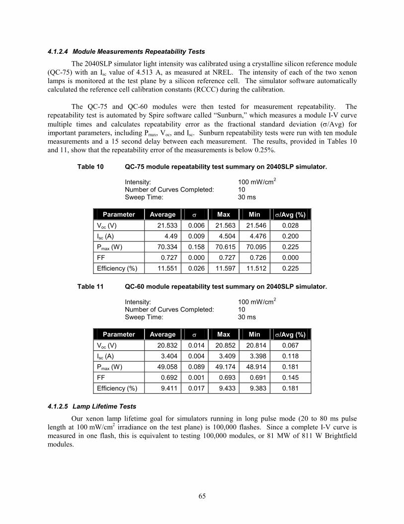
4.1.2.4 Module Measurements Repeatability Tests
The 2040SLP simulator light intensity was calibrated using a crystalline silicon reference module (QC-75) with an Isc value of 4.513 A, as measured at NREL. The intensity of each of the two xenon lamps is monitored at the test plane by a silicon reference cell. The simulator software automatically calculated the reference cell calibration constants (RCCC) during the calibration.
The QC-75 and QC-60 modules were then tested for measurement repeatability. The repeatability test is automated by Spire software called “Sunburn,” which measures a module I-V curve multiple times and calculates repeatability error as the fractional standard deviation (σ/Avg) for important parameters, including Pmax, Voc, and Isc. Sunburn repeatability tests were run with ten module measurements and a 15 second delay between each measurement. The results, provided in Tables 10 and 11, show that the repeatability error of the measurements is below 0.25%.
Table 10 QC-75 module repeatability test summary on 2040SLP simulator.
Intensity: 100 mW/cm2 Number of Curves Completed: 10 Sweep Time: 30 ms
Parameter Average σ Max Min σ/Avg (%)
Voc (V) 21.533 0.006 21.563 21.546 0.028 Isc (A) 4.49 0.009 4.504 4.476 0.200 Pmax (W) 70.334 0.158 70.615 70.095 0.225 FF 0.727 0.000 0.727 0.726 0.000 Efficiency (%) 11.551 0.026 11.597 11.512 0.225
Table 11 QC-60 module repeatability test summary on 2040SLP simulator.
Intensity: 100 mW/cm2 Number of Curves Completed: 10 Sweep Time: 30 ms
Parameter Average σ Max Min σ/Avg (%)
Voc (V) 20.832 0.014 20.852 20.814 0.067 Isc (A) 3.404 0.004 3.409 3.398 0.118 Pmax (W) 49.058 0.089 49.174 48.914 0.181 FF 0.692 0.001 0.693 0.691 0.145 Efficiency (%) 9.411 0.017 9.433 9.383 0.181
4.1.2.5 Lamp Lifetime Tests
Our xenon lamp lifetime goal for simulators running in long pulse mode (20 to 80 ms pulse length at 100 mW/cm2 irradiance on the test plane) is 100,000 flashes. Since a complete I-V curve is measured in one flash, this is equivalent to testing 100,000 modules, or 81 MW of 811 W Brightfield modules.
65

Two series of tests were initiated to evaluate the expected lifetime of the xenon lamps. In the first series, xenon lamp lifetime testing was done with our long-pulse lamp electronics installed on a simulator with a single 1.955 m long lamp, illuminating a 1.0 m x 1.6 m test plane. The simulator was operated continuously, flashing every 15 seconds, 24 hours per day. The lamp pulse width was approximately 100 ms and the irradiance at the test plane was 100 mW/cm2. The lamp was still flashing reliably after 164,000 flashes, significantly exceeding our goal for nominal lamp life of 100,000 flashes. Figure 83 shows a typical plot of lamp intensity, module voltage, and module current measured during a single lamp flash. This data was captured from the Test Information screen, part of the long-pulse simulator’s graphical user interface (GUI).
06-039WA
Figure 83 Plot of lamp intensity, module voltage, and module current, from the long pulse
simulator’s Test Information screen.
In the second series of tests, still underway at the time this report was written, the lamp exceeded 120,000 flashes at 1 sun with no significant change in lamp spectral output. Extra capacitance was added to the lamp power supply for this test, so each flash had a 175 ms pulse width at 1 sun. This is more than double the 80 ms pulse width specification for our long pulse solar simulators.
We monitored the maximum pulse width that the lamp generated at one sun irradiance as the lamp aged. The pulse width was essentially the same (175 ms) after 120,000 flashes as it was when the lamp was new, using the same lamp capacitor voltage.
A plot of data collected over the first 100,000 long-pulse lamp flashes is shown in Figure 84. Here we plot module short circuit current and lamp irradiance in two wavelength bins, the blue region of the spectrum (400 to 500 nm) and the infrared region (900 to 1100 nm), as a fraction of total lamp irradiance. In our experience, these are the two wavelength bins most subject to change with lamp aging.
Table 12 lists the averages of the Isc and irradiance data plotted in Figure 84 over the first 10,000 flashes and after 90,000 flashes. There is essentially no change (0.1%) in module Isc, while the irradiance in the blue wavelength bin decreased 2.3% and the infrared wavelength bin increased 4.8%, as a fraction of total irradiance. Figure 82 shows that these spectral changes are small enough that the simulator maintains its Class A rating.
66
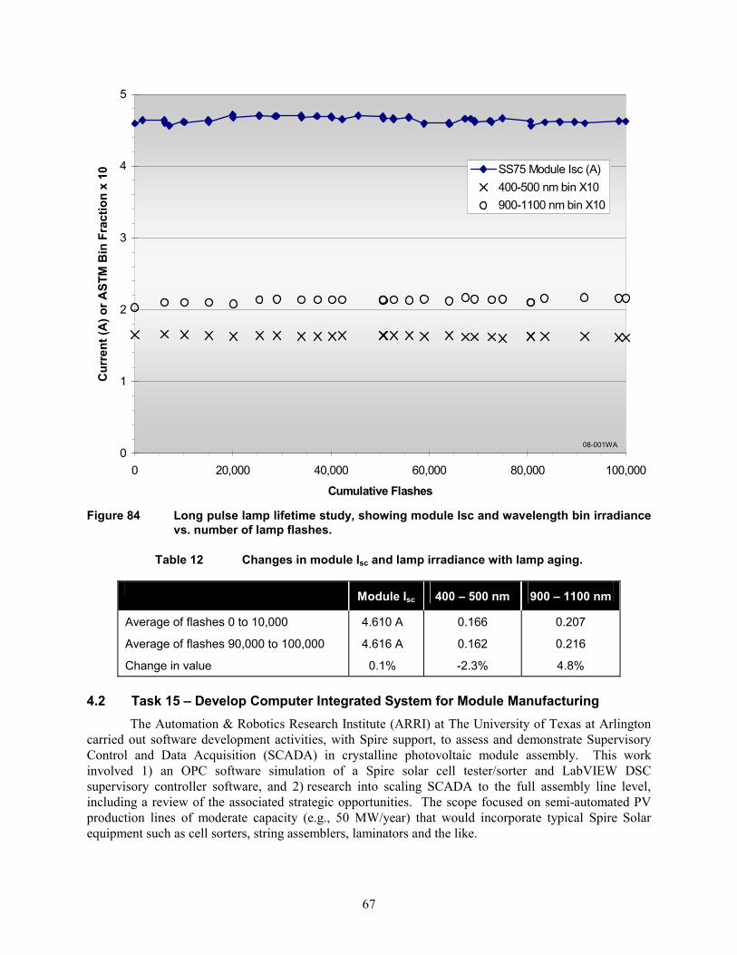
0
1
2
3
4
5
0 20,000 40,000 60,000 80,000 100,000
Cumulative Flashes
Cur
rent
(A) o
r AST
M B
in F
ract
ion
x 10
SS75 Module Isc (A)400-500 nm bin X10900-1100 nm bin X10
08-001WA
Figure 84 Long pulse lamp lifetime study, showing module Isc and wavelength bin irradiance vs. number of lamp flashes.
Table 12 Changes in module Isc and lamp irradiance with lamp aging.
Module Isc 400 – 500 nm 900 – 1100 nm
Average of flashes 0 to 10,000
Average of flashes 90,000 to 100,000
C hange in value
4.610 A
4.616 A
0.1%
0.166
0.162
-2. % 3
0.207
0.216
4.8% 4.2 Task 15 – Develop Computer Integrated System for Module Manufacturing
The Automation & Robotics Research Institute (ARRI) at The University of Texas at Arlington carried out software development activities, with Spire support, to assess and demonstrate Supervisory Control and Data Acquisition (SCADA) in crystalline photovoltaic module assembly. This work involved 1) an OPC software simulation of a Spire solar cell tester/sorter and LabVIEW DSC supervisory controller software, and 2) research into scaling SCADA to the full assembly line level, including a review of the associated strategic opportunities. The scope focused on semi-automated PV production lines of moderate capacity (e.g., 50 MW/year) that would incorporate typical Spire Solar equipment such as cell sorters, string assemblers, laminators and the like.
67

4.2.1 SCADA Software Prototype
Following an overall analysis of the SCADA field and an assessment within the PV assembly context, ARRI’s principal software development task was to prototype a specific but typical scenario of executive work cell control for solar module manufacturing. The equipment target for the demonstration was Spire’s solar cell tester-sorter, representing a moderately complex piece of automation using a PC with highly customized software as a front-end controller. This choice for the development activity satisfied two fundamental needs. First, it required the prototype to address and employ all the SCADA functions of interest: interprocess communications, graphical interfaces, handling of different data types and transmission rates, bidirectional flow of information, alarming, and databasing. Second, its functionality is scalable and ultimately applicable to all foreseeable factory platforms, ranging from simple HMI (human-machine interface) screens, to PLC-driven devices, to quality control oriented stations, and finally to the most complex multi-axis module assemblers. Table 13 summarizes the objectives of this task.
Table 13 Software prototype demonstration objectives.
Relevant SCADA Functions Equipment Targets of Interest
• Interprocess communications • Graphical interfaces • Handling of all major data types • Bidirectional information flow
(machine↔supervisor) • Alarming and databasing
• Simple HMI panels (operator interfaces) • PLC-controlled devices; material conveyance • Quality control-oriented equipment • Low-complexity assembly equipment • High-complexity (multi-axis) assembly
equipment 4.2.1.1 Interprocess Communications Layer
An interprocess communications layer is a requirement for SCADA development because of the wide range of factory equipment with which an executive controller must communicate. The uncontested standard within the realm of the PC platform is OLE for Process Control (OPC). This is an open, industry consortium-led framework based on Microsoft’s Object Linking and Embedding (OLE) technology (ActiveX). OPC leverages the operating system itself to provide built-in capability for information sharing between applications. In the case at hand, these applications represent the typically single SCADA executive (OPC client) and multiple information sources (OPC servers) which are physically attached to sensors and controllers. Based on these considerations, OPC compliance was considered a necessity.
Many providers of PLC controllers, GPIB-based test equipment, and “intelligent” sensor devices (for example, those with internet browsing front ends) provide out-of-the-box OPC capability, which can quickly be enabled and interfaced to the SCADA executive. However, the more sophisticated Spire Solar equipment, though equipped with PLCs or other equivalent dedicated sensor and motion hardware, was designed to have a Windows PC driving the graphical user interface, machine I/O, and master program logic, usually programmed in VisualBasic. Further, although Spire had produced some custom-made implementations using Dynamic Data Exchange, no interprocess communication capability was built in. ARRI’s first step was to establish a way to provide this function based on OPC standards, and to do so with minimal disruption to Spire’s investment in the existing code.
68

Among the strengths of a standard like OPC is extensive third-party support, and it was indeed found that products existed in the market to satisfy the specific need of embedding OPC functionality in custom-developed VisualBasic programs. ARRI identified and evaluated two candidates in this category: Slik-Da from Northern Dynamics, and OPCServerX from Metadynamics. The OPCServerX product was selected and purchased, and ARRI wrote a customized VisualBasic application using the InstantOPC ActiveX component to simulate the OPC data traffic and server interaction generated by a working Spire solar cell tester/sorter.
Figure 85 illustrates the concepts and approach presented above. The architecture is that of a Windows PC providing dedicated control of all cell sensor/actuator functions, user interface, and communications. External control modules (e.g., servomotor drives) provide functions requiring hard real-time response, such as motion tracking of electric actuators. Some of these controllers could themselves be OPC servers, and could in principle be accessed directly from a SCADA supervisor. However, in the proposed configuration, all control remains subservient to the PC, and an OPC “stub” is embedded into the VisualBasic application to enable SCADA functionality for the entire work cell.
Modem (diagnostics)
Controller Cabinet
Industrial Windows PC
PLC (e.g. Allen-Bradley) and/or Motion Controller (e.g. Parker 6K)
RS-232 / RS-488 devices
Data acquisition boards
Shop Floor Ethernet
Interprocess Communication(OPC Server)
Master Executable (VisualBasic)
PV Manufacturing Equipment Hardware
Figure 85 Representative PV assembly equipment control architecture and OPC embedding.
4.2.1.2 Spire Cell Tester-Sorter Simulator
A program was written to emulate an OPC-enabled cell tester, consisting of a simple window to display diagnostic output (e.g., when an OPC client connects and disconnects from the server, or requests an update from a particular piece of data) and an infinite loop that would generate messages involving various data types (Boolean, integer, double, string) with mixed periodicity (every 5, 10, and 15 seconds). These represent the variable updates that would occur in the course of regular equipment operation. Although a user interface was provided for convenience in this case, typical OPC implementations do not display any such activity; the OPC layer runs quietly in the background and is available to software clients upon request.
69
In all, over fifty process variables were set up for interaction with the executive controller. In order to illustrate and take advantage of the group/item hierarchy established by the OPC standard, these variables were clustered under the categories of machine safety, machine status, machine process, cell test results, machine control, and machine parameters.
Interaction with the Metadynamics OPCServerX libraries requires a few programming steps which may easily be embedded into an existing application. ARRI provided a fully documented set of source code to Spire that can be used to implement an OPC-compliant application. Such applications can provide OPC exposure to any number of internal variables in an otherwise-unaware VisualBasic program. This mechanism has relevance beyond the scope of this subcontract in regards to implementing a SCADA supervisor. The use of OPC provides a standards-based, effective pathway for Spire equipment to interoperate with any data acquisition, supervisory control or MES software – whether provided by Spire or by third parties. 4.2.1.3 SCADA Executive
The SCADA executive component of this project was implemented using LabVIEW with Data and Supervisory Control (DSC) extensions from National Instruments. The development effort involved the generation of graphical user interfaces and accompanying code to interact with the cell tester/sorter mock-up module described in the preceding sections.
The primary objectives of the SCADA executive are to establish connections to one or several OPC servers (which are the equipment data sources), capture multiple streams of information in quasi-real time, display items of interest in a local (or possibly remote, through telephony or internet) graphical user interface, insert relevant information in a permanent repository, and monitor specific variables of interest to indicate alarms or otherwise noteworthy thresholds. Under non-real time conditions, the SCADA package can host programs to produce any number of data analyses and reports, or these can be sourced from different applications via standardized database interfaces (e.g., ODBC or SQL). In LabVIEW, the Citadel database application provides basic data browsing capability.
The GUI for this software prototype is mostly illustrative, and it would likely be simpler in design for an actual implementation. Although LabVIEW and other mainstream SCADA packages have very rich graphic libraries and controls that exceed native VisualBasic in ease and performance (something which is part of their overhead), the use of detailed graphics to support monitoring and control of all machine functions from a remote station would not make much sense when a local GUI is already available. It is customary in SCADA, however, to take advantage of the graphical utilities to canvas the screen with realistic and intuitive backdrops, such as actual machine photographs and mechanical drawings on which indicators are superimposed.
In our case, a main screen (Figure 86) was created to display fundamental status, process, and safety indicators. For status, the machine light tree is reproduced, and basic indicators report on power and utilities. Process information is conveyed by displaying the number of solar cells in each sorting bin, as well as total cell count. Safety and machine guarding information is shown by rectangular LED blocks that light up according to the state of pressure mats and doors.
70

Figure 86 Main LabVIEW development window for SCADA demonstration.
Note that there is not necessarily a one-to-one correspondence between every indicator and a source variable from the machine’s OPC server. The SCADA software has the capacity to keep track of machine states distilled from source variables, and display, alarm, and database these no differently than any other variable in the system. How this is split between the source equipment and the SCADA supervisor is always a software design decision; factors to consider include how critical the information is and who can most faithfully generate it, whether it causes undue network traffic, and whether the computational burden is more logically assigned to the machine or to the supervisor. The important point is that SCADA software—and a package like LabVIEW in particular—does have the ability to do significant local data processing to reduce, combine, or otherwise enhance the source information received over OPC.
The prototype GUI also includes three pushbuttons, labeled “Start,” “Stop,” and “Calibrate.” These buttons represent actions that the SCADA supervisor would request of the target machine, something that always needs careful attention in remote control scenarios. As before, these involve system design decisions that must consider utility and safety implications. This functionality is included in the prototype to illustrate not so much remote control of a single, sophisticated machine, but rather the potential in the software for bidirectional information flow. This can be highly relevant in full-up line control scenarios, for example, to control conveyors, gate material flow, or pause/restart upstream equipment based on downstream conditions.
The “Events and Alarms” display is a typical and important component of a SCADA application. It reports on system-level events (e.g., a user has logged in) or on variables that exceed a particular threshold. LabVIEW provides the ability to drop default event/alarm lists onto the GUI with minimal programming.
71

The final component of interest in the main screen is represented by a button cluster for different views. An important and powerful feature of the GUI in SCADA applications is to provide different modes of interaction and visualization of the equipment being supervised, depending on the information domain of interest to the user. The main view, as shown above, might be thought of as a default display showing common process and safety indicators. Other additional views are proposed, including (a) process view: manufacturing effectiveness of system – throughput, utilization, downtime, events, alarms; (b) product view: manufactured product characteristics – cell quantity, cell quality, correlation with equipment performance; (c) maintenance view: machine health monitoring, predictive maintenance, extended events and alarms affecting machine uptime.
The process of generating a LabVIEW DSC application is straightforward, but requires familiarization with National Instruments “graphical programming” paradigm. The fundamental element of a LabVIEW application is the Virtual Instrument, or VI, which couples a user interface and a functional block diagram to perform a particular input-output process. The block diagram is a graphical representation of the logic that the VI performs, and VIs are interconnected to produce working programs according to “data flow” rules: any one block commences execution as soon as all its input data is available, and any number of blocks will execute simultaneously (unless otherwise forced by the programmer). This is very different from the traditional procedural programming, where flow of execution is intrinsically dictated by the order of the program lines, unless branching instructions specify otherwise.
Native LabVIEW contains an extensive library of VIs to perform all manner of numerical data manipulation, flow control, matrixing, and other common program building and OS-related (e.g., TCP/IP stack) functions. In addition, as a mathematics and analysis-oriented package, it also makes available a wide collection of high quality libraries for signal processing, statistical analysis, and graphing and charting, sound, etc. The Data and Supervisory Control (DSC) extensions, which constitute National Instruments’ formal product offering in this arena, ride on top of LabVIEW’s full functionality to provide SCADA-oriented capabilities, such as data server management, tag management (a tag is a variable in SCADA parlance), event and alarm management, and database connectivity. Also indigenous to DSC are user login authentication and data security attribute management, which provide controlled and safe access to both programs and data.
The process of creating a SCADA application in LabVIEW, once the GUI design has been established, involves connecting to a data source (typically via OPC), creating “tags” to hold the individual data items acquired from the source, and finally associating graphical elements with tags. LabVIEW’s Tag Configuration Editor is the starting point to do this. Each tag is configured for data type, flow direction, group, update rate, deadband (to make lower network traffic and storage demands when no significant change occurs), and alarming thresholds, among others. Figure 87 shows a screen capture of a typical LabVIEW VI graphical code segment, where common program control structures (e.g., the master continuous execution loop on top) and other components are associated with the GUI of Figure 86. 4.2.2 Scaling SCADA to a Full PV Module Production Line
The fundamental nature of a SCADA package can be viewed as monitoring and controlling a production line as if it were a single machine, in the same way that a PLC causes a series of sensors and actuators to behave as a single entity, and yet in the same way that a resource planning system causes the whole of manufacturing equipment, materials and other support functions to operate as a single “production” entity. This is the functional need that the SCADA market is geared to satisfy.
72

Figure 87 Typical LabVIEW graphical program.
SCADA is not generally prescribed for single machine monitoring and control as presented in the previous section, whose intent was exploring and demonstrating the capabilities of VisualBasic-hosted OPC and LabVIEW. Although some SCADA applications amply justify themselves on the basis of providing a remote user interface for large, monolithic processing equipment (e.g., a chemical reactor, or a power generating unit), this is not useful for the typical equipment in a Spire PV module manufacturing line. Using the SCADA supervisor to replicate GUI and control functionality already available at the local machine does not add value. The reasons are the likely proximity of the machine to the control center (and thus operational redundancy), the availability of operators on the floor, and the obvious safety implications of issuing commands remotely, with the sole exception of a start/pause function, which arises in a different context. This assessment would change as the size of the line grows larger, and as it becomes automated to the point of displacing human intervention. At this level, SCADA would, in fact, be a natural choice to host the main GUI and many control functions for each piece of equipment in the line.
The true leverage of SCADA in PV module manufacturing occurs when multiple machines in the assembly line are connected to a central system. The two benefits that arise from this condition are:
1. The central system acts as a data concentrator with a uniform interface; this enables and encourages the long-term storage of any production data, standardizes the information processing algorithms (scripts, or programs for reduction and analysis) and QC databasing functions, and increases the safety and integrity of the information.
2. An infrastructure is provided for machines to have awareness, and take advantage of, knowledge
of upstream and downstream conditions in the line, and thus operate in a closed-loop fashion.
73
The first point is a logistical one. SCADA merely facilitates the retention and processing of data that would have otherwise been lost due to the effort required to capture it (e.g., installing a front-end PC with custom-written software), or strengthens the integrity of data already being collected through standardization and centralized storage, particularly from QC-oriented equipment.
The second point presents a fundamental paradigm shift from the current state of PV module production, which involves the serialization of otherwise isolated pieces of production equipment. Under a SCADA supervisor, it would suddenly become possible to execute line control in earnest, from simple line pacing and balancing (e.g., pausing and starting machines to maintain an optimal product flow) to sophisticated on-the-fly recipe downloading and other closed-loop process tuning and control functions.
Before exploring this point further, a question arises as to the difficulty of accomplishing this degree of machine integration. How complicated a task would it be to add more pieces of equipment in the same manner as the cell tester? As the machine count increases, the increase in infrastructural complexity is logarithmic, not exponential. The reason the per-machine effort diminishes as more pieces are added lies in being able to reuse the code to retrofit and connect equipment. The OPC and LabVIEW development techniques are exactly the same, whether the controller is Windows PC-based or PLC-based. To be fair, in implementing the more advanced SCADA functions, the interactions between higher numbers of machines do imply higher algorithmic complexity, but not from a perspective of setting the infrastructure in place. The OPC standard is mainly responsible for this fortunate situation – it is simple, universally embraced, and designed to handle thousands of data points without transmission speed penalties. Furthermore, because OPC is hosted within a network-compliant OS, it has full Ethernet capability, and this is the physical layer for which every PC and any modern PLC or robot controller is already set up.
SCADA implementations should not be, and are not required to be, latency critical – this is to say, there are no real-time performance concerns. Therefore, a standard (10/100 Mbit/s) local network with its own bridge/router (it is always advisable to isolate shop floor-oriented machines from the outside internet) provides the physical connection and no specialty fieldbuses are necessary. For a PV module production application, integrating multiple machines into a SCADA supervisor requires the lowest conceivable hardware investment.
Figure 88 illustrates this concept, depicting a generic, full-up PV module assembly line under a common SCADA supervisor. (In sophisticated or high-volume scenarios, having more than one supervisor is possible.) A combination of OPC data sources (servers) is shown, all using Ethernet as the physical transmission medium. The sources include (a) HMI operator screens, which are PC-hosted and OPC enabled (e.g., Cutler-Hammer PanelMate, CTC Parker Interact, Rockwell PanelView); (b) PLCs, which may drive simpler devices such as glass washers, module buffers, or conveyors; (c) PC-hosted QC equipment; and (d) complex PC-hosted (motion control / robotics) equipment. Data clients beyond the main supervisor are also represented, including the possibility of separate, dedicated data repositories.
74
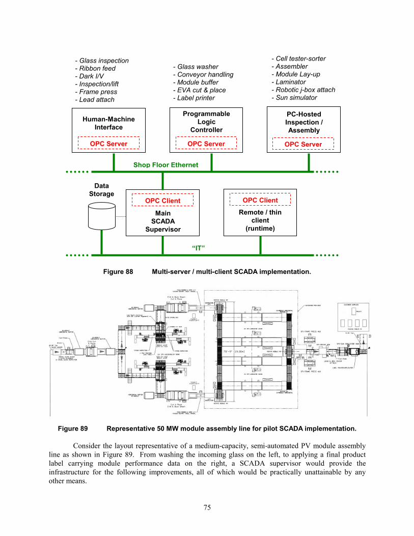
- Cell tester-sorter - Assembler
- Glass inspection - Glass washer - Ribbon feed
- Module Lay-up - Conveyor handling - Dark I/V - Laminator - Robotic j-box attach - Sun simulator
- Module buffer - Inspection/lift - EVA cut & place - Frame press - Label printer - Lead attach
Figure 88 Multi-server / multi-client SCADA implementation.
Figure 89 Representative 50 MW module assembly line for pilot SCADA implementation.
Consider the layout representative of a medium-capacity, semi-automated PV module assembly line as shown in Figure 89. From washing the incoming glass on the left, to applying a final product label carrying module performance data on the right, a SCADA supervisor would provide the infrastructure for the following improvements, all of which would be practically unattainable by any other means.
Data Storage
Main SCADA
Supervisor
OPC ClientRemote / thin
client (runtime)
OPC Client
Shop Floor Ethernet
“IT”
Programmable PC-Hosted Human-Machine
Interface Logic Inspection /
Assembly Controller
OPC Server OPC Server OPC Server
75

1. Production Effectiveness SCADA could provide a “dashboard” for the performance of the entire production line, both in terms of the equipment utilization itself, and the intervention of operators. Metrics that could easily be captured or synthesized in real-time include:
• Total cell and module production counts • Defect / reject rate • Idle time • Product flow bottlenecks • WIP and buffer utilization • Occurrence of “disruptive” or undesirable events: violation of safety interlocks, time to
restore regular production, etc.
With SCADA HMI capabilities, furthermore, digital diagnostic and repair manuals could be provided for use by operators to expedite fault recovery, with no security concerns through proper use of user authentication features in the software. Off-line, measures of overall production line performance, individual equipment performance, bottleneck sites / frequency / severity, etc., could be deduced from the above information.
2. Machine Health Monitoring This is the individual equipment view of the previous section,
expanded to take into account predictive measures and ultimately reduce the likelihood of unanticipated failure and production loss, or impact on product quality. The data that can be used for this purpose can range from simple production counts (number of times a xenon lamp has flashed) to sophisticated analyses of user-settable machine parameters or analog profiles, such as friction-compensating time delays (increasing? deteriorating?) in certain motion components, or the vacuum pump-down signature in a laminator (leaks? degraded pump?).
3. Production Monitoring This activity considers the correlation between product and process
variables. Does the condition of the production equipment affect the quality or variability in the product, and if so, how? Can a particular machine parameter be traced to an increase or a decrease in the quality, or fault / reject rate, of the product that is flowing through it? What is the tolerance window, for a particular process variable, within which stable product output is known to occur? Being able to first mine these relationships, and then monitor them on-line according to simplified rules, would have significant potential to increase production yields.
4. Intelligent Manufacturing This can be viewed as the “enlightened” state of manufacturing,
where the real-time feedback of process and product information, combined with historical knowledge, causes the entire production line to behave in a self-regulated, intelligent manner. The external manifestation of this state is optimized, uninterrupted single-piece flow, not because nothing ever breaks down, but because predictive equipment and process models are sufficiently accurate to eliminate variability (uncertainty); few unscheduled events occur, and the manufacturing process is predictable. This lies at the opposite end of the spectrum of serialized automation islands, where we’ve gone from a state of zero knowledge of the “whole line” behavior, and transformed data from individual pieces of equipment into useful and actionable information.
Note that the above benefits are not attainable out-of-the-box with any commercial SCADA
package: all of the above functions entail writing custom-developed code. SCADA does, however, provide the infrastructure necessary for efficient implementation, and it does so with power to spare. The degree of sophistication of said applications would heavily influence the choice of the underlying SCADA package (e.g., LabVIEW, CTC Parker, Genesis, etc.) for its scripting and analytical capabilities.
76

It is conceivable that generic “applets” could be written for the PV module assembly industry, as self-standing products, leveraging OPC and standardizing on certain machine functions, to implement some of the applications described in this section (similar to GEM/SECS and the follow-on CAMX efforts which focus on the semiconductor industry). 4.3 Task 16 – Development of Low-stress Cell String Assembly Processes
Spire Solar evaluated a number of low-stress high-throughput cell string assembly processes in this task. Some of the improvements we developed are already being implemented in our production equipment for cell stringing and cell testing and sorting. These developments are described in the following sections. 4.3.1 New Machine Design
Spire’s current solar cell stringing machines solder one cell at a time with infrared energy. We are planning to develop a significantly different soldering process for our next generation solar cell stringing machine (called the Spi-Assembler 12K) that will solder entire strings, up to 2.5 m long, at one time under a uniform infrared (IR) heat source. The goal is increased throughput but the main driving factor in this type of equipment is maximizing yield. The objective is to create a machine that causes less stress and breakage during processing. Normally the single cell method requires about 6 seconds to solder a cell, including index time. This is the bottleneck in the machine. We believe that by soldering an entire string at once we can fabricate a string much faster, using about 3 seconds per cell to place the cells and ribbon into a fixture. For a ten-cell string, this allows a full 30 seconds to slowly ramp up the heat to create the solder joint. This slow, even heating produces lower thermal stress and fewer fractures.
We produced a prototype system to evaluate the feasibility of this concept by developing a soldering process on strings up to 91 cm (36 inches) long. The system design, shown in Figure 90, consists of a 30 cm x 91 cm IR panel heater mounted on a pair of parallel servomotor-driven slides. A tray for holding cell strings is mounted below the heater on a hand-operated slide that operates like a drawer, for loading strings and moving them under the heater. Both the panel heater and the string tray can be attached in the orientation shown, or they can be rotated 90°, to test various process techniques.
Heater slide
Figure 90 CAD design for string soldering test set-up.
String tray IR panel heater
Heater slide
07-004WA
Tray slide
77

The CAD model, assembly drawings, and detail drawings for the prototype soldering system were completed and components were released for fabrication and procurement. Figure 91 shows the IR soldering unit suspended on the moving portion of the frame. A thermally insulating nest made from a high temperature material was designed and fabricated to hold and align a cell string for soldering. The oven can be indexed over the string to solder it.
Figure 91 String alignment fixture and IR heating system.
Spire Solar’s engineering group developed a method of integrating of this new soldering concept into a functional automated machine. The initial concept is illustrated in Figure 92.
07-013WA
06-034WA
Figure 92 Initial concept for an automated cell string soldering system.
78

Cells are loaded from stack carriers, aligned by machine vision, and placed on one of two vacuum platens. The platens hold the ribbons and cells in place prior to soldering, and index as the cell string is constructed. Once the string is fully assembled, it will move into an infrared oven where the entire string is soldered at one time. Some advantages of the new system include:
• Speed – we can make strings as fast as we can place cells and ribbons, theoretically 1200 to 1300 cells per hour. The soldering process is no longer the limit.
• High yield for thin cells – by using an oven with spatially uniform heating we reduce the thermal stress on the cells. We can also take advantage of slower heating and cooling, if necessary, since we are processing an entire string (typically 9 to 12 cells), not single cells.
• Eliminate a string alignment step – the string is always located by vacuum on a pallet, so we don't lose control of its position, and no longer need to align it before placing it in a module.
• Eliminate preheat platens – complex and costly heated platens are gone. We use a thermally neutral material for the platen and heat from above slowly. The conveying system is relatively simple.
• Cost – this system has some low cost features. The layout and mechanics are fairly simple. The main cost drivers will be the loading robot with machine vision and the soldering oven.
• Intelligent heating – active thermal analysis could be provided inside the oven to detect hot and cold zones. We would actively modify heater settings to improve temperature uniformity and obtain more consistent solder joints.
• Space – this design has a small footprint and may be even more compact that our existing stringer.
• Changeover for different cells or strings – cell pallets, for loading, and string pallets, for soldering, are made with quick-change inserts. Ribbons are robotically placed in the desired locations. Changeover would actually be a few minutes, possibly without any tools.
Designs were more fully developed and a detailed three-dimensional CAD model was completed.
The model, shown in Figure 93, is the concept for the proposed system and the design basis for our next generation cell-stringing machine.
IR ovenCell load robot
Figure 93 View from a CAD model for an automated high-throughput cell string soldering
system.
Cell pallet conveyor
String assembly
shuttle
Ribbon load robot
Ribbon handling assembly
07-016WA
79

4.3.2 Back Contact Cells
As part of this work, we developed a concept for automating the cell interconnection process for back contact solar cells. Sample quantities of back contact cells and special metal tabs used to connect them in series were obtained from a manufacturer and evaluated. Several engineering group meetings were held to define a machine concept.
Based on our evaluations, several of the new subsystems being designed for the Spi-Assembler 12K can be adopted for back contact cells, including the cell loader (which uses a pallet conveyor and SCARA robot), machine vision cell aligner, linear string assembly shuttles, string soldering oven, and string unloader. Given the unique requirements of back contact cells, new systems were conceptualized for tab feeding, flux application, tab cutting, and tab pick-and-place to the string assembly shuttles. A concept drawing for a complete, automated stringing system was completed.
The concept, shown in Figure 94, incorporates several new subsystems being designed for our next-generation cell-stringing machine (the Spi-Assembler 12K), including the cell loader (which uses a pallet conveyor and SCARA robot), machine vision cell aligner, two linear string assembly shuttles, string soldering oven (described in Section 3.2), and string unloader. Given the unique requirements of back contact cells, new systems were conceptualized for tab feeding, flux application, tab cutting, and tab pick-and-place to the string assembly shuttles.
Figure 94 Concept for an automated back contact cell string soldering machine.
An engineering concept drawing (Spire drawing no. A210-0502) for an automated stringing system for back contact cells was completed and delivered to NREL in December 2006.
80
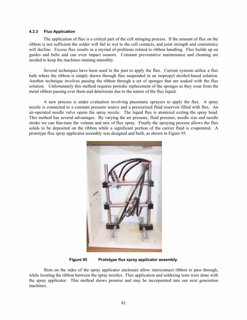
4.3.3 Flux Application
The application of flux is a critical part of the cell stringing process. If the amount of flux on the ribbon is not sufficient the solder will fail to wet to the cell contacts, and joint strength and consistency will decline. Excess flux results in a myriad of problems related to ribbon handling. Flux builds up on guides and belts and can even impact sensors. Constant preventative maintenance and cleaning are needed to keep the machines running smoothly.
Several techniques have been used in the past to apply the flux. Current systems utilize a flux bath where the ribbon is simply drawn through flux suspended in an isopropyl alcohol-based solution. Another technique involves passing the ribbon through a set of sponges that are soaked with the flux solution. Unfortunately this method requires periodic replacement of the sponges as they wear from the metal ribbon passing over them and deteriorate due to the nature of the flux liquid.
A new process is under evaluation involving pneumatic sprayers to apply the flux. A spray nozzle is connected to a constant pressure source and a pressurized fluid reservoir filled with flux. An air-operated needle valve opens the spray nozzle. The liquid flux is atomized exiting the spray head. This method has several advantages. By varying the air pressure, fluid pressure, needle size and needle stroke we can fine-tune the volume and mix of flux spray. Finally the spraying process allows the flux solids to be deposited on the ribbon while a significant portion of the carrier fluid is evaporated. A prototype flux spray applicator assembly was designed and built, as shown in Figure 95.
Figure 95 Prototype flux spray applicator assembly. Slots on the sides of the spray applicator enclosure allow interconnect ribbon to pass through, while locating the ribbon between the spray nozzles. Flux application and soldering tests were done with the spray applicator. This method shows promise and may be incorporated into our next generation machines.
81
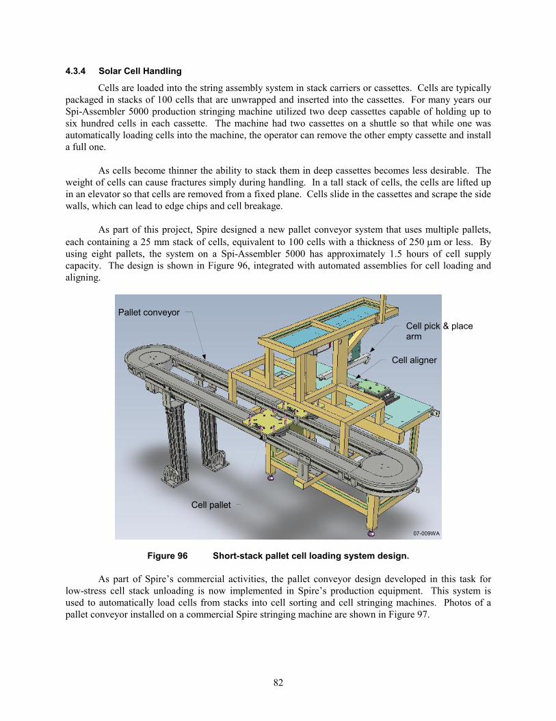
4.3.4 Solar Cell Handling
Cells are loaded into the string assembly system in stack carriers or cassettes. Cells are typically packaged in stacks of 100 cells that are unwrapped and inserted into the cassettes. For many years our Spi-Assembler 5000 production stringing machine utilized two deep cassettes capable of holding up to six hundred cells in each cassette. The machine had two cassettes on a shuttle so that while one was automatically loading cells into the machine, the operator can remove the other empty cassette and install a full one.
As cells become thinner the ability to stack them in deep cassettes becomes less desirable. The weight of cells can cause fractures simply during handling. In a tall stack of cells, the cells are lifted up in an elevator so that cells are removed from a fixed plane. Cells slide in the cassettes and scrape the side walls, which can lead to edge chips and cell breakage.
As part of this project, Spire designed a new pallet conveyor system that uses multiple pallets, each containing a 25 mm stack of cells, equivalent to 100 cells with a thickness of 250 μm or less. By using eight pallets, the system on a Spi-Assembler 5000 has approximately 1.5 hours of cell supply capacity. The design is shown in Figure 96, integrated with automated assemblies for cell loading and aligning.
Pallet conveyor
Cell pallet
Cell pick & place arm
Cell aligner
07-009WA
Figure 96 Short-stack pallet cell loading system design.
As part of Spire’s commercial activities, the pallet conveyor design developed in this task for
low-stress cell stack unloading is now implemented in Spire’s production equipment. This system is used to automatically load cells from stacks into cell sorting and cell stringing machines. Photos of a pallet conveyor installed on a commercial Spire stringing machine are shown in Figure 97.
82

07-025WA
Figure 97 Cell pallet conveyor installed on an automated cell stinging machine.
An oval conveyor configuration is used to transport full pallets into the machine and return empty pallets back to a location where an operator can refill them. The new design reduces the weight of the stack on the cells by reducing the stack height to 25 mm. In addition, the vertical side walls used in the tall stack carrier were replaced with tapered pins to eliminate edge rubbing when the cells are lifted from the stack. The combination of reduced weight on the cells and reduced edge rubbing results in a lower stress unloading process for the cells. The pallet conveyor allows multiple pallets of short cell stacks to be loaded, maintaining the large cell load capacity of the tall stacks.
One of the hurdles to overcome when using the new pallet system is the ability to repeatedly remove one cell at a time from the stack with minimal cell breakage. Lifting the cells from cassettes without damage becomes more difficult as cells become thinner. By nature cells form a vacuum between adjacent cells and tend to stick together when one cell is lifted vertically from a stack. Often two or three cells will be lifted at once. The extra cells may or may not simply fall off during cell transport causing cell breakage and machine handling errors.
There are several techniques used to lift a single cell without breaking it. Vacuum cups are typically used to lift the cell while air nozzles or air knives blow air at the top edge of the cell stack in order to eliminate the vacuum formed between two cells in intimate contact. This can cause the top few cells to float, which eliminates the vacuum but can cause cell damage if the cells oscillate back and forth. Another technique involves bending the cells to eliminate the vacuum. Very slight curvature of the cells is needed, perhaps 1 mm from center to edge. This assists the process but normally must be used in conjunction with air knives to achieve production speeds.
A new cell pickup hand was tested that is unique in that several techniques are combined in a novel way. This assembly has four vacuum cups located to pick up the cell on its outermost edges. The vacuum cups collapse slightly when they make contact with the cell, which causes the cell edges to lift up approximately 1 mm. A central bar supports the center of the cell to create a slight bend. The vacuum hand has sufficient height compliance that we can eliminate the stack elevator used in our present cell stack loader. The pick-up hand is shown in Figure 98.
83
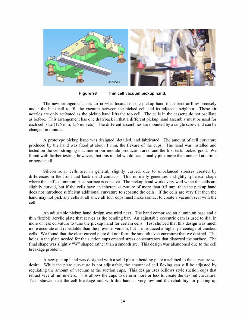
06-038WA
Figure 98 Thin cell vacuum pickup hand.
The new arrangement uses air nozzles located on the pickup hand that direct airflow precisely
under the bent cell to fill the vacuum between the picked cell and its adjacent neighbor. These air nozzles are only activated as the pickup hand lifts the top cell. The cells in the cassette do not oscillate as before. This arrangement has one drawback in that a different pickup hand assembly must be used for each cell size (125 mm, 156 mm etc). The different assemblies are mounted by a single screw and can be changed in minutes.
A prototype pickup hand was designed, detailed, and fabricated. The amount of cell curvature produced by the hand was fixed at about 1 mm, the flexure of the cups. The hand was installed and tested on the cell-stringing machine in our module production area, and the first tests looked good. We found with further testing, however, that this model would occasionally pick more than one cell at a time or none at all.
Silicon solar cells are, in general, slightly curved, due to unbalanced stresses created by differences in the front and back metal contacts. This normally generates a slightly spherical shape where the cell’s aluminum back surface is concave. The pickup hand works very well when the cells are slightly curved, but if the cells have an inherent curvature of more than 0.5 mm, then the pickup hand does not introduce sufficient additional curvature to separate the cells. If the cells are very flat then the hand may not pick any cells at all since all four cups must make contact to create a vacuum seal with the cell.
An adjustable pickup hand design was tried next. The hand comprised an aluminum base and a thin flexible acrylic plate that serves as the bending bar. An adjustable eccentric cam is used to dial in more or less curvature to tune the pickup hand for certain cells. Test showed that this design was much more accurate and repeatable than the previous version, but it introduced a higher percentage of cracked cells. We found that the clear curved plate did not form the smooth even curvature that we desired. The holes in the plate needed for the suction cups created stress concentrators that distorted the surface. The final shape was slightly “W” shaped rather than a smooth arc. This design was abandoned due to the cell breakage problem.
A new pickup hand was designed with a solid plastic bending plate machined to the curvature we desire. While the plate curvature is not adjustable, the amount of cell flexing can still be adjusted by regulating the amount of vacuum at the suction cups. This design uses bellows style suction cups that retract several millimeters. This allows the cups to deform more or less to create the desired curvature. Tests showed that the cell breakage rate with this hand is very low and the reliability for picking up
84
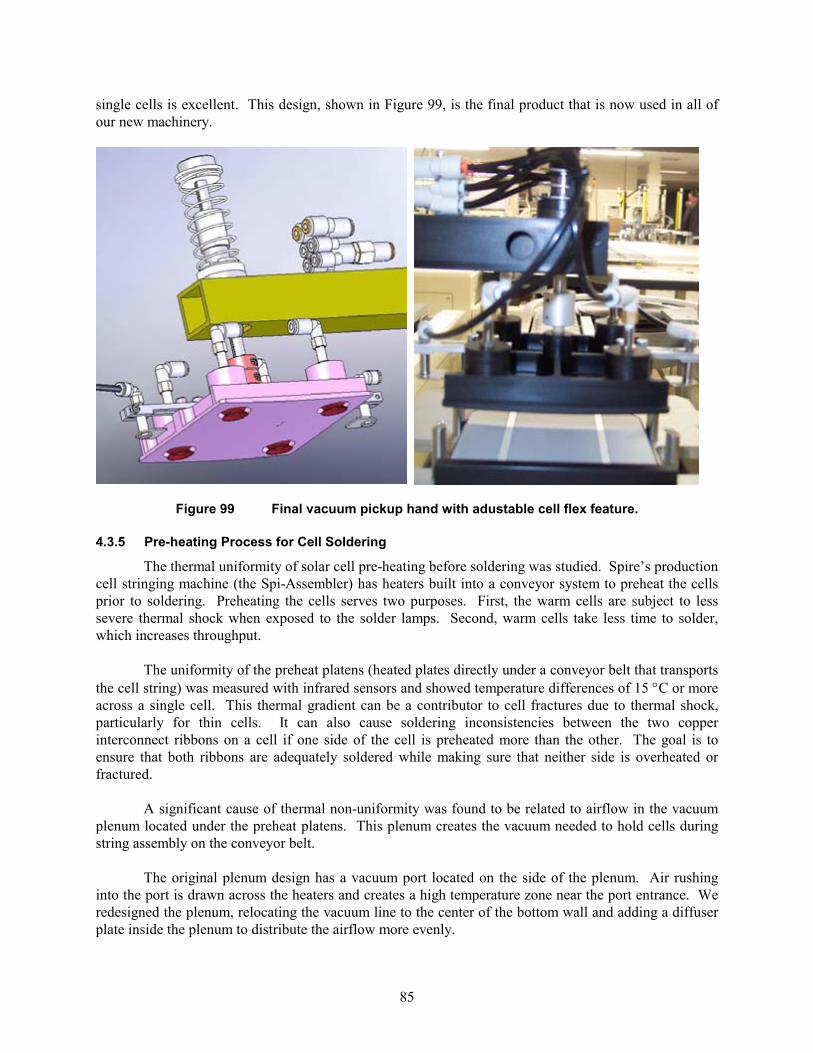
single cells is excellent. This design, shown in Figure 99, is the final product that is now used in all of our new machinery.
Figure 99 Final vacuum pickup hand with adustable cell flex feature. 4.3.5 Pre-heating Process for Cell Soldering
The thermal uniformity of solar cell pre-heating before soldering was studied. Spire’s production cell stringing machine (the Spi-Assembler) has heaters built into a conveyor system to preheat the cells prior to soldering. Preheating the cells serves two purposes. First, the warm cells are subject to less severe thermal shock when exposed to the solder lamps. Second, warm cells take less time to solder, which increases throughput.
The uniformity of the preheat platens (heated plates directly under a conveyor belt that transports the cell string) was measured with infrared sensors and showed temperature differences of 15 °C or more across a single cell. This thermal gradient can be a contributor to cell fractures due to thermal shock, particularly for thin cells. It can also cause soldering inconsistencies between the two copper interconnect ribbons on a cell if one side of the cell is preheated more than the other. The goal is to ensure that both ribbons are adequately soldered while making sure that neither side is overheated or fractured.
A significant cause of thermal non-uniformity was found to be related to airflow in the vacuum plenum located under the preheat platens. This plenum creates the vacuum needed to hold cells during string assembly on the conveyor belt.
The original plenum design has a vacuum port located on the side of the plenum. Air rushing into the port is drawn across the heaters and creates a high temperature zone near the port entrance. We redesigned the plenum, relocating the vacuum line to the center of the bottom wall and adding a diffuser plate inside the plenum to distribute the airflow more evenly.
85

We then fabricated, installed, and tested the new plenum. The modifications reduced the thermal gradient at the solder position significantly, as shown in Figure 100, where the maximum thermal gradient across a 156 mm square cell is 5.9°C. String soldering tests showed even temperatures at both interconnect ribbons and improved soldering strength and consistency. This change is now integrated into all new production machines.
Max:temp 94.2
Min:temp 88.3
86.3
115.4 °C
90
95
100
105
110
115
FLIR Systems
07-003WA
Figure 100 Infrared image of a cell string on a heated platen.
4.3.6 Ribbon Corrugator
Development work for a prototype ribbon corrugator for soldering thin cells with low stress was done under Task 11 of this program. Higher cell yields (less silicon breakage) were observed when corrugated ribbon was used on thin cells. More recent cell soldering work done at Spire with 220 μm thick 156 mm square multicrystalline silicon cells from a major solar cell producer showed that these thin cells are significantly less curled after soldering with corrugated ribbon, when compared to the same cells soldered with conventional flat ribbon. These results are good indicators of reduced stress after soldering when using corrugated ribbon.
Given these positive results, as part of our commercial activities, we are upgrading our prototype ribbon corrugator mechanism to make it suitable for production use. Improvements were made to provide more precise control of the corrugation depth adjustment and to improve ribbon guiding through the mechanism. Corrugator assembly and detail drawings were completed and parts were procured, fabricated and assembled. Corrugator assemblies were installed on a production cell-stringing machine for testing. We will complete our evaluations with Spire internal R&D funds, and plan to offer corrugation as an option to our customers in the near future.
86

5 CONCLUSIONS Spire completed a three-phase program for developing automated production line processes for
solar Brightfield modules. In Phase 1, a large area (1.57 m x 3.68 m) 800 W module for utility-scale PV arrays was designed, with emphasis on minimizing Balance of System (BOS) costs. Unique module features include internally laminated by-pass diodes, which greatly simplify the internal busing and the output terminals, and a cantilevered superstrate that allows for a reduced glass thickness and a simpler frame design.
The design of automated tools began for producing such modules in multi-megawatt per year quantities. A cell string inspection system with machine vision and microcrack detection capabilities was developed and tested. An advanced lamination process was developed with a faster-curing EVA for increased laminator throughput, and improvements were made to reduce laminator maintenance and downtime. Automated systems were designed for dispensing and laying up module materials (EVA and back sheet) and for installing and soldering bus ribbons and diodes prior to lamination.
In Phase 2 we designed and developed automated tools for producing Brightfield modules in multi-megawatt per year quantities. Major achievements include the following:
• An automated system for dispensing and laying up module materials (encapsulant and back sheet) was fabricated and tested. The system feeds sheet material, cuts it to length, and places it in position directly on the module. An in-line punch cuts a narrow rectangular hole along one edge of the sheet for feeding bus leads through to the module output boxes. Testing was done to measure the accuracy of cut lengths, hole locations, and sheet placement on the module for stable and elastomeric sheets.
• We fabricated and tested an automated system for installing and soldering bus ribbons and diodes in modules prior to lamination. The system comprises two machines, a bus ribbon fabrication machine and a bus and diode installation machine.
o The bus ribbon fabrication machine automatically feeds ribbon from reels, straightens it to remove coil set, cuts or punches it to length, and fills a tray with a stack of ribbon. The punch trims one end of the bus to match the diode width, to prevent the positive and negative bus leads from shorting out the diode.
o The bus and diode installation system consists of a conveyor and aligner for 1.6 m x 3.7 m modules and a 4-axis robot with a custom multi-tool end-effector for placing bus ribbon, applying flux, placing diodes, and soldering bus ribbons. The robot also places reusable insulator strips on the module to prevent the encapsulant from melting during the soldering process. Spire’s unique hot-bar solder tip was used for soldering the cell string ribbons and the diodes to the bus ribbons. Solder joint pull strengths far exceeded the 450 g target value when pulled at a 90° angle and in shear.
• We designed an advanced vacuum laminator for large PV modules. The lamination area (2.0 m x 4.0 m) is more than twice the size of our current largest model. Vacuum chamber structural design work was done using finite element analysis to optimize the chamber structure while maintaining deflection and stress within acceptable limits. A new heated platen design was conceived in which a blanket heater is used in place of rod heaters for improved temperature uniformity. A module pin lift design was incorporated to prevent glass bowing during the initial pump-out phase of the lamination cycle. A quick-release diaphragm clamp system was designed to reduce equipment downtime during diaphragm replacement. A vertical cover lift was designed to reduce the time needed for loading and unloading modules.
87
• Mechanical design work was completed for an automated conveyor system for transporting modules through the large area laminator (2 m x 4 m module size capacity). The drive components for the conveyor were sized and selected. Mechanical design models, assembly drawings, and detail drawings were created for the drive conveyor and a motor-driven conveyor cleaning brush assembly.
• We designed a solar simulator with a 2.0 m x 4.0 m large test area for measuring the electrical performance of the Brightfield module under simulated sunlight. This test area is nearly three times the size of our current largest simulator. We used a flash-up geometry to simplify product handling by allowing modules to be transported over the simulator on a conveyor. The simulator has four 2 m long xenon lamps positioned side-by-side under the test plane. Adjustable reflecting surfaces direct light to the test plane, while optical filters correct the spectrum to Air Mass 1.5 Global, per ASTM E927-05.
o We developed a single-flash, long pulse xenon light source for the solar simulator, in place of our standard multiple-flash short-pulse xenon lamp. The single flash shortens the measurement time from ~20 s to less than 1 s per module. The long pulse increases the illumination time up to 100 ms, compared to our standard 1 ms pulse, to allow the simulator to measure the performance of high efficiency and thin film modules with slow illumination response.
o A unique active lamp control scheme was devised for the long pulse lamp. Lamp intensity is controlled by active feedback from a reference cell. Extremely flat, well-controlled pulses up to 78 ms were demonstrated. Tests showed the temporal instability of irradiance is 0.1%, which is an order of magnitude better than that obtained with a passive pulse-forming network. The pulse length can be increased to 100 ms or beyond simply by increasing the capacitance of the lamp circuit.
• We demonstrated a method for forming shallow, fine-pitch features in thick copper ribbon to reduce stress and maintain high yield in the cell string soldering process. We designed an automated ribbon forming assembly that was installed in our automated cell string assembly equipment. This equipment successfully assembled cell strings made with 220 μm thick Cz-Si cells and 178 μm thick copper ribbon. This technology can be applied to reduce the breakage rate of thin cells in the string soldering process, and to allow the use of thicker copper ribbon to reduce module power loss due to ribbon series resistance.
In Phase 3 we completed the design work for a solar simulator with a 2 m x 4 m test area, nearly
three times the area of our largest current simulators. We also developed a single-flash long-pulse xenon light source in place of our standard multiple-flash short-pulse xenon lamp. The single flash shortens the measurement time from ~20 s to less than 1 s per module. The long pulse illuminates the module for up to 100 ms, compared to our standard 1 ms flash, which enables more accurate testing of high efficiency and thin film modules with slow response times. We successfully commercialized the single long pulse technology in our solar simulator product line, having sold over 60 long pulse simulators to PV module manufacturers and test laboratories, representing approximately 80% of our simulator sales.
We completed mechanical, electrical, and software design work on the large area solar simulator, designated the Spi-Sun Simulator 2040SLP. Engineering assembly drawings, detail drawings, wiring schematics, circuit board artwork, and bills of materials were completed. Components were fabricated and procured, and the 240SLP was assembled and tested.
88

The electronics and software for the single-flash, long-pulse xenon light source were extensively tested. A new high power electronic load was developed and tested for I-V curve measurements under single long-pulse conditions. These tests resulted in a number of upgrades to the electronics and software for improved and more robust operation. In addition, hardware and software was developed and tested for multiple lamp control, using reference cells for closed-loop irradiance feedback. A new lamp mounting assembly was designed that reduces the mechanical stress on the lamp seals while reducing the time needed to change a lamp.
We developed a new simulator function for measuring two IV curves at two light intensities in a single flash. This technique is useful for making accurate module series resistance (Rs) measurements, using the method in IEC standard 608915. Measurements made with the new dual intensity technique showed Rs reproducibility error (σ/average) is typically < 1%, an order of magnitude improvement over the slope near Voc method.
The Spi-Sun Simulator 2040SLP was tested and characterized by measuring its spatial uniformity of irradiance, temporal stability of irradiance, spectral match to the Air Mass 1.5 Global solar spectrum, module I-V measurement repeatability, and lamp lifetime. Spatial uniformity measurements were made on an optical test bed with the same xenon lamps and optics as the 2040SLP. After tuning the optics we achieved 1.7% spatial uniformity of irradiance over a 1 m x 2 m test plane, which is the area illuminated by one lamp. Similar work was then done on a second xenon lamp in the test bed, and we achieved 1.6% spatial uniformity of irradiance over an adjacent 1 m x 2 m test plane illuminated by the second lamp.
The effectiveness of the 2040 SLP’s active lamp control circuitry was verified by irradiance stability measurements. The light pulse irradiance was measured over a 50 ms period and the temporal instability was found to be 0.11%. This value greatly exceeds the Class A requirements for ASTM and IEC standards, which specify a temporal instability of 2% or less.
Simulator spectral irradiance measurements were made with dual spectrometers and an
integrating sphere located near the center of the test area. We integrated the total energy of each wavelength band from 400 nm to 1100 nm and compared the data with the values specified by the IEC and ASTM standards for the Air Mass 1.5 Global solar spectrum. The simulator’s spectral irradiance was within Class A limits over the entire spectrum.
Two PV modules were tested for measurement repeatability using automated Spire software that measures a module I-V curve multiple times and calculates repeatability error as the fractional standard deviation (σ/average) for important parameters, including Pmax, Voc, and Isc. The results showed that the repeatability error of the measurements was less than 0.25%.
Two series of tests were done to evaluate the expected lifetime of the xenon lamps. In the first series, the lamp pulse width was approximately 100 ms at 1 sun irradiance. The lamp was still flashing reliably after 164,000 flashes, significantly exceeding our goal for nominal lamp life of 100,000 flashes. In the second series of tests, the lamp exceeded 120,000 flashes with a 175 ms pulse width. The pulse width was the same after 120,000 flashes as it was when the lamp was new. We monitored module short circuit current and lamp irradiance vs. wavelength as the lamp aged. After 100,000 flashes, there was essentially no change in module Isc, and only minor changes in the blue (-2.3%) and the infrared (+4.8%) regions, allowing the simulator to maintain its Class A spectrum.
89
The Automation & Robotics Research Institute (ARRI) developed a Computer Integrated Manufacturing strategy for Spire’s photovoltaic module manufacturing lines. ARRI implemented two VisualBasic and LabVIEW DSC applications that emulated the interaction between a production tool (the Spire Cell Sorter) and Supervisory Control and Data Acquisition (SCADA) executive software, using OPC for communication. The Cell Sorter is a moderately complex piece of automation, chosen to give a complete picture of user interaction modes and data exchange capabilities found in this class of software.
This approach can be extrapolated from a single machine to a multi-station automated production line scenario. The modularity and network transparency of the SCADA software would allow us to scale this application to include cell stringers/assemblers, laminators, sun simulators, and other module processing and test equipment in a straightforward manner. At this level, entirely new strategic opportunities for SCADA arise that do not exist in single-device implementations. These opportunities were identified with a view to maximizing the benefits of a prospective SCADA investment.
We evaluated a number of low-stress high-throughput cell string assembly processes. Some of the improvements we developed are already implemented in our production equipment for cell stringing and cell testing/sorting. The following is a summary of our accomplishments in this task.
• A new batch cell string soldering concept was devised, which decouples the soldering process from the parts assembly process to minimize thermal stress and maximize throughput.
• A liquid flux spray process was evaluated for improving the consistency of flux application to ribbons for soldering.
• A short stack pallet cell loading system was developed which reduces mechanical stress on thin cells by 1) reducing the cell stack height from 150 mm to 25 mm and 2) eliminating rubbing of cell edges by removing a cell elevator and using tapered stack guides. This improved system is now used in our production machines for cell stringing and cell testing/sorting.
• A new vacuum pickup hand was developed for picking up thin cells from a 25 mm high stack with high reliability and yield. This improvement is now used in our production machines for cell stringing and cell testing/sorting.
• A new automated string assembly system was designed, incorporating low-stress process technologies such as short stack cell loading, thin cell pickup from a stack, non-contact cell alignment, interconnect ribbon corrugation, and batch string soldering. It is designed to handle solar cells as thin as 150 to 200 µm at production rates of 1200 cells per hour.
• A concept was developed for applying low-stress high-speed string soldering techniques to silicon back contact cells.
• A more uniform cell pre-heating process was developed, in which improved airflow uniformity in a vacuum plenum resulted in significantly more uniform cell temperatures. This improvement is now used in our cell stringing production machines.
90

6 REFERENCES
1. Tedlar® is a registered trademark of DuPont for its polyvinyl fluoride (PVF) film.
2. Teflon® is a registered trademark of DuPont for its fluoropolymer film.
3. ASTM E927-05 “Standard Specification for Solar Simulation for Photovoltaic Testing,” ASTM International, West Conshohocken, PA, May 2005.
4. IEC 60904-9 Edition 2.0 “Photovoltaic devices – Part 9: Solar simulator performance requirements,” International Electrotechnical Commission, Geneva, Switzerland, Oct 2007.
5. IEC 60891, “Procedures for temperature and irradiance corrections to measured I-V characteristics of crystalline silicon photovoltaic devices,” International Electrotechnical Commission, Geneva, Switzerland, 1987; see Clause 4, Determination of internal series resistance.
91
F1146-E(09/2007)
REPORT DOCUMENTATION PAGE Form Approved OMB No. 0704-0188
The public reporting burden for this collection of information is estimated to average 1 hour per response, including the time for reviewing instructions, searching existing data sources, gathering and maintaining the data needed, and completing and reviewing the collection of information. Send comments regarding this burden estimate or any other aspect of this collection of information, including suggestions for reducing the burden, to Department of Defense, Executive Services and Communications Directorate (0704-0188). Respondents should be aware that notwithstanding any other provision of law, no person shall be subject to any penalty for failing to comply with a collection of information if it does not display a currently valid OMB control number. PLEASE DO NOT RETURN YOUR FORM TO THE ABOVE ORGANIZATION. 1. REPORT DATE (DD-MM-YYYY)
April 2008 2. REPORT TYPE
Subcontract Report 3. DATES COVERED (From - To)
1 June 2003 to 30 Nov 2007 5a. CONTRACT NUMBER
DE-AC36-99-GO10337
5b. GRANT NUMBER
4. TITLE AND SUBTITLE Development of Automated Production Line Processes for Solar Brightfield Modules: Final Report, 1 June 2003-30 November 2007
5c. PROGRAM ELEMENT NUMBER
5d. PROJECT NUMBER NREL/SR-520-43190
5e. TASK NUMBER PVB75301
6. AUTHOR(S) M. Nowlan
5f. WORK UNIT NUMBER
7. PERFORMING ORGANIZATION NAME(S) AND ADDRESS(ES) Spire Corporation One Patriots Park Bedford, MA 01730-2396 USA
8. PERFORMING ORGANIZATION REPORT NUMBER ZDO-3-30628-12
10. SPONSOR/MONITOR'S ACRONYM(S) NREL
9. SPONSORING/MONITORING AGENCY NAME(S) AND ADDRESS(ES) National Renewable Energy Laboratory 1617 Cole Blvd. Golden, CO 80401-3393 11. SPONSORING/MONITORING
AGENCY REPORT NUMBER NREL/SR-520-43190
12. DISTRIBUTION AVAILABILITY STATEMENT National Technical Information Service U.S. Department of Commerce 5285 Port Royal Road Springfield, VA 22161
13. SUPPLEMENTARY NOTES NREL Technical Monitor: Brian Keyes
14. ABSTRACT (Maximum 200 Words) This report summarizes the progress made by Spire Corporation under NREL’s PV Manufacturing R&D Project Subcontract No. ZDO-3-30628-12, to develop new automated systems for fabricating very large photovoltaic (PV) modules. Spire addressed the project goals of improving PV manufacturing processes and products while reducing costs and providing a technology foundation that supports significant manufacturing scale-up. To accomplish this, Spire focused efforts on the design of a large-area utility-scale module and the development of the necessary manufacturing techniques and equipment to manufacture such a module in a high-volume production environment.
15. SUBJECT TERMS PV; manufacturer; automated production line processes; modules; large-area; utility scale; high volume; arrays
16. SECURITY CLASSIFICATION OF: 19a. NAME OF RESPONSIBLE PERSON a. REPORT
Unclassified b. ABSTRACT Unclassified
c. THIS PAGE Unclassified
17. LIMITATION OF ABSTRACT
UL
18. NUMBER OF PAGES
19b. TELEPHONE NUMBER (Include area code)
Standard Form 298 (Rev. 8/98) Prescribed by ANSI Std. Z39.18