development of an ac to dc converter using microcontroller - ethesis
52
DEVELOPMENT OF AN AC TO DC CONVERTER USING MICROCONTROLLER A project report submitted in partial fulfillment of the requirements for the degree of Bachelor of Technology in Electrical Engineering By RASHMI RANJAN ROUT DURGA PRASAD TRIPATHY National Institute of Technology, Rourkela Rourkela-769008, Orissa.
Transcript of development of an ac to dc converter using microcontroller - ethesis

DEVELOPMENT OF AN AC TO DC CONVERTER USING MICROCONTROLLER
A project report submitted in partial fulfillment of the requirements for the degree of
Bachelor of Technology in Electrical Engineering
By
RASHMI RANJAN ROUT
DURGA PRASAD TRIPATHY
National Institute of Technology, Rourkela
Rourkela-769008, Orissa.

DEVELOPMENT OF AN AC TO DC CONVERTER USING MICROCONTROLLER
A project report submitted in partial fulfillment of the requirements for the degree of
Bachelor of Technology in Electrical Engineering
By
RASHMI RANJAN ROUT (10502029)
DURGA PRASAD TRIPATHY (10502058)
Under the guidance of
PROFESSOR J. K. SATAPATHY,
Department of Electrical Engineering,
NIT Rourkela.
National Institute of Technology, Rourkela
Rourkela-769008, Orissa.

ACKNOWLEDGEMENT
We would like to express our gratitude towards all the people who have contributed their precious time and effort to help us. Without them it would not have been possible for us to understand and complete the project. We would like to thank Professor J.K.Satapathy, Department of Electrical Engineering, our Project Supervisor for his guidance, support, motivation and encouragement through out the period this work was carried out. His readiness for consultation at all times, his educative comments, his concern and assistance even with practical things have been invaluable. We would also like to express our heart-felt gratitude to the faculty of Electrical Engineering Department for providing a challenging and enlightening experience. We remain indebted to National Institute of Technology, Rourkela for providing us this platform of excellence. A project of this nature could never have been attempted without our reference to and inspiration from the works of others whose details are mentioned in the References section. We acknowledge our indebtedness to all of them. Last, but not the least, our sincere thanks to all of our friends who have patiently extended all sorts of help for accomplishing this undertaking. Date: Rashmi Ranjan Rout (10502029) Durga Prasad Tripathy (10502058)

Department of Electrical Engineering,
National Institute of Technology, Rourkela.
Rourkela-769008, Orissa.
CERTIFICATE
This is to certify that the thesis entitled, “DEVELOPMENT OF A PROTOTYPE OF AC TO DC CONVERTER FOR THE ELECTRICAL DEPARTMENT USING MICROCONTROLLER” submitted by Rashmi Ranjan Rout for the partial fulfillment of the requirements for the award of Bachelor of Technology degree in Electrical Engineering at the National Institute of Technology, Rourkela (Deemed University) is an authentic work carried out by him under my supervision and guidance.
To the best of my knowledge the matter embodied in the thesis has not been submitted to any other University/Institute for the award of any degree or diploma.
Date: Professor J. K. Satapathy,
Department of Electrical Engineering,
National Institute of Technology, Rourkela
Rourkela-769008, Orissa.

Department of Electrical Engineering,
National Institute of Technology, Rourkela.
Rourkela-769008, Orissa.
CERTIFICATE
This is to certify that the thesis entitled, “DEVELOPMENT OF A PROTOTYPE OF AC TO DC CONVERTER FOR THE ELECTRICAL DEPARTMENT USING MICROCONTROLLER” submitted by Durga Prasad Tripathy for the partial fulfillment of the requirements for the award of Bachelor of Technology degree in Electrical Engineering at the National Institute of Technology, Rourkela (Deemed University) is an authentic work carried out by him under my supervision and guidance.
To the best of my knowledge the matter embodied in the thesis has not been submitted to any other University/Institute for the award of any degree or diploma.
Date: Professor J. K. Satapathy,
Department of Electrical Engineering,
National Institute of Technology, Rourkela
Rourkela-769008, Orissa.

CONTENTS
Page
Acknowledgement i Certificate ii, iii
Contents iv,v,vi
List of Figures vii,viii
Abstract ix
1. Introduction 1
2. Insulated Gate Bipolar Transistor (IGBT) 4
2.1 Advantages & disadvantages of IGBT 5
2.1.1 Advantages 5
2.1.2 Disadvantages 5
2.2 Equivalent Circuit of IGBT 6
2.3 Working Principle 7
2.4 Latch-up in IGBT 7
2.5 IGBT characteristics 7
2.5.1 Static I-V characteristics 7
2.5.2 Transfer characteristics 8
2.5.3 Switching characteristics 9
3. Basic components and their Interfacing techniques 10
3.1 ATMEGA32L-8PU (AVR Series microcontroller) 11

3.1.1 Important Features 11
3.1.2 PIN Configuration 12
3.1.3 Programming AVR Microcontroller 13
3.1.4 Installation of WINAVR Software 13
3.1.5 MAKEFILE Specifications 13
3.1.6 Installation of AVRDUDE 13
3.2 Components used 14
3.3 Softwares used 14
3.4 Operation of the converter 15
3.4.1 Basic Function 15
3.4.2 Voltage Control by the Knob 16
3.4.3 Circuit Schematic 17
4. Simulation in Multisim (N.I.) 18
4.1 Simulation Circuit Diagram 19
4.2 Simulation Results 20
5. Voltage Control Using PID Algorithm 23
5.1 The Proportional-Integral-Derivative (PID) algorithm 24
5.1.1 A Proportional algorithm 24
5.1.2 A Proportional Integral algorithm 25
5.1.3 A Proportional Integral Derivative algorithm 25
5.2 The characteristics of P, I and D controllers 26
5.3 PID implementation on Output voltage control 27
5.3.1 Determination of Average output voltage 28
5.3.2 PID implementation 28
5.3.3 The Plant Model 29

5.3.4 Proportional Integral Derivative control (PID) 31
5.3.5 Application of Proportional control (P) 31
5.3.6 Application of Proportional Integral control (PI) 32
5.3.7 Application of Proportional-Integral-Derivative control (PID) 33
5.3.8 Simulation of output voltage in Simulink 34
5.3.9 Load resistance measurement 36
5.3.10 Voltage control across the load due to AC voltage fluctuation 37
Conclusion 38
References 40

LIST OF FIGURES
Figure Page Figure 2.1 Structure of IGBT 6
Figure 2.2 Equivalent circuit of IGBT 6
Figure 2.3 Static I-V characteristics of IGBT 8
Figure 2.4 IGBT Transfer Characteristics 8
Figure 2.5 Switching Characteristics of IGBT 9
Figure 3.1 PIN Configuration of Atmega32 Microcontroller 12
Figure 3.2 Graetz Bridge and smoothing capacitor 15
Figure 3.3 Circuit diagram of an AC to DC converter using microcontroller 17
Figure 4.1 Simulation circuit in Multisim 19
Figure 4.2 Output for a load of 1K-ohms and duty cycle 90% 20
Figure 4.2 Output for a load of 1K-ohms and duty cycle 60% 20
Figure 4.2 Output for a load of 1K-ohms and duty cycle 30% 21
Figure 4.2 Output for a load of 500 ohms and duty cycle 90% 21
Figure 4.2 Output for a load of 500 ohms and duty cycle 60% 22
Figure 4.2 Output for a load of 500 ohms and duty cycle 30% 22
Figure 5.1 Block diagram of a plant with a controller 26 Figure 5.2 Block diagram of a PID controller 27 Figure 5.3 Measurement of output voltage by microcontroller 28
Figure 5.4 Plant Model 29 Figure 5.5 Open loop response 30 Figure 5.6 Response due to Proportional control 31

Figure 5.7 Response due to P-I control 32 Figure 5.8 Response due to P-I-D control 33 Figure 5.9 Simulink Block diagram 34
Figure 5.10 Voltage variation due to load change without control 35 Figure 5.11 Voltage variation with P-I-D control 35 Figure 5.12 Calculation of load resistance 36

ABSTRACT The aim of the project is to obtain a controlled DC output from a standard single phase 230V, 50Hz power supply. For this we first rectified the ac voltage using four diodes. Then the rectified DC voltage is used to get controlled DC voltage output using an IGBT with a pulse of variable duty cycle, generated by a microcontroller. By varying the duty cycle of the square wave pulse the average output DC voltage is regulated. For user interfacing, a knob is used to set the required voltage. This is achieved by converting the analog signal input, from the knob, to digital signal by using the internal Analog to Digital converter present in the microcontroller. The microcontroller sets the duty cycle of the PWM wave according to the ADC value obtained. This PWM wave is given as input to the IGBT to regulate its duty cycle, and hence the average output voltage is regulated. This is basically the open loop regulation of voltage. If the load varies, then we have to use closed loop control to automatically increase the duty cycle of the gate pulse to the IGBT if the output voltage falls below a set point and vice versa. The negative feedback loop is based on PID loop control. Thus the output voltage is continuously tuned with the set point voltage.

1
Chapter 1
INTRODUCTION

2
Many industrial applications make use of controlled DC power, like in steel rolling mills, paper mills and textile mills, which employ DC motor drives. The basic advantages of DC motor are high starting torque, high accelerating and decelerating torque. DC motor is easily adaptable for drives requiring wide range speed control and quick reversals. So DC machine possesses high degree of flexibility and versatility. The losses like eddy current loss, hysteresis loss are also absent in DC applications. For some industrial applications a versatile AC to DC converter is indispensable. Direct current is used to charge batteries, and in nearly all electronic systems as the power supply. Very large quantities of direct-current power are used in production of aluminum and other electrochemical processes. Direct current is also used for some railway propulsion, especially in urban areas. High voltage direct current (HVDC) is used to transmit large amounts of power from remote generation sites or to interconnect alternating current power grids.
DC is commonly found in many low-voltage applications, especially where these are powered by batteries, which can produce only DC, or solar power systems, since solar cells can produce only DC. Most automotive applications use DC, although the alternator is an AC device which uses a rectifier to produce DC. Most electronic circuits require a DC power supply. Applications using fuel cells (mixing hydrogen and oxygen together with a catalyst to produce electricity and water as byproducts) also produce only DC. Many telephones connect to a twisted pair of wires, and internally separate the AC component of the voltage between the two wires (the audio signal) from the DC component of the voltage between the two wires (used to power the phone). Telephone exchange communication equipment, such as DSLAM, uses standard -48V DC power supply. The negative polarity is achieved by grounding the positive terminal of power supply system and the battery bank. This is done to prevent electrolysis depositions. An electrified third rail can be used to power both underground (subway) and overground trains.
Direct-current installations usually have different types of sockets, switches, and fixtures, mostly due to the low voltages used, from those suitable for alternating current. It is usually important with a direct-current appliance not to reverse polarity unless the device has a diode bridge to correct for this.
In our model we have used one IGBT and four diodes to convert AC to DC, which is cost efficient. Power conversion applications consist of an AC-to-DC conversion stage immediately following the AC source. The DC output obtained after rectification is subsequently used for further stages. Current pulses with high peak amplitude are drawn from a rectified voltage source with sine wave input and capacitive filtering. Increasing demands for higher power density, smaller size, more portability and more flexible systems spur industry to continuously design new generations of AC-DC power supplies using power devices with the lowest switching and conduction losses to increase efficiency, reduce thermal problems and improve power density. We have preferred IGBT over other semi-converter devices like thyristor, BJT etc., because of lower gate drive requirements, lower switching losses of the IGBT and some other reasons stated

3
later. The turn-off process of IGBT is simple, compared to thyristor, as it does not require any commutation below the rated threshold collector current.
The aim of the project is to obtain a controlled DC output from a standard single phase 230V, 50Hz power supply. For this we first rectified the AC voltage using four diodes. Then the rectified DC voltage is used to get controlled DC voltage output using an IGBT with a pulse of variable duty cycle, generated by a microcontroller. By varying the duty cycle of the square wave pulse the average output DC voltage is regulated. For user interfacing, a knob is used to set the required voltage. This is achieved by converting the analog signal input, from the knob, to digital signal by using the internal Analog to Digital converter present in the microcontroller. The microcontroller sets the duty cycle of the PWM wave according to the ADC value obtained. This PWM wave is given as input to the IGBT to regulate its duty cycle, and hence the average output voltage is regulated. This is basically the open loop regulation of voltage. If the load varies, then we have to use closed loop control to automatically increase the duty cycle of the IGBT if the output voltage falls below a set point and vice versa. The negative feedback loop is based on PID loop control. Thus the output voltage is continuously tuned with the set point voltage.

4
Chapter 2
INSULATED GATE BIPOLAR
TRANSISTOR (IGBT)

5
We are using Insulated Gate Bipolar Transistor (IGBT) for conversion of AC to controlled DC in our work. IGBT has been developed by combining into it the best qualities of both BJT and MOSFET. IGBT is also called Metal Oxide Insulated Gate Transistor (MOSIGT), Conductively Modulated Field Effect Transistor (COMFET) or Gain Modulated FET (GEMFET).
2.1 Advantages & disadvantages of IGBT over other semiconductor devices
2.1.1 Advantages
• IGBT possesses high input impedance like a MOSFET.
• IGBT possesses low on-state power loss as in a BJT. • IGBT is free from the secondary breakdown problem that is present in BJT. • IGBT possesses lower gate drive requirements.
• IGBT has smaller snubber circuit requirements. • IGBT converters are more efficient with less size as well as cost, as compared to
converters based on BJTs. • Switching losses in IGBTs are lesser. • Device rise and fall time switching capability is 5-10 times faster, resulting in
lower device switching loss and a more efficient drive. • The IGBT being a voltage rather than current controlled gate device has a lower
base drive circuit cost that also results in lower drive package cost.
• Higher switching frequencies of IGBT drives produce less peak current ripple, thus producing less current harmonic motor heating and allowing rated motor torque with lower peak current than BJT drives.
2.1.2 Disadvantages
• For a similar motor cable length as the BJT drive, the faster output voltage rise time of the IGBT drive may increase the dielectric voltage stress on the motor and cable due to a phenomenon called reflected wave.
• Faster output dv/dt transitions of IGBT drives also increase the possibility for phenomenon such as increased common mode electrical noise.
• Electromagnetic interference (EMI) problems and increased capacitive cable charging current problems.
• Any pulse width modulated (PWM) drive with a steep fronted output voltage wave form may increase motor shaft voltage and lead to a bearing current phenomenon known as fluting.
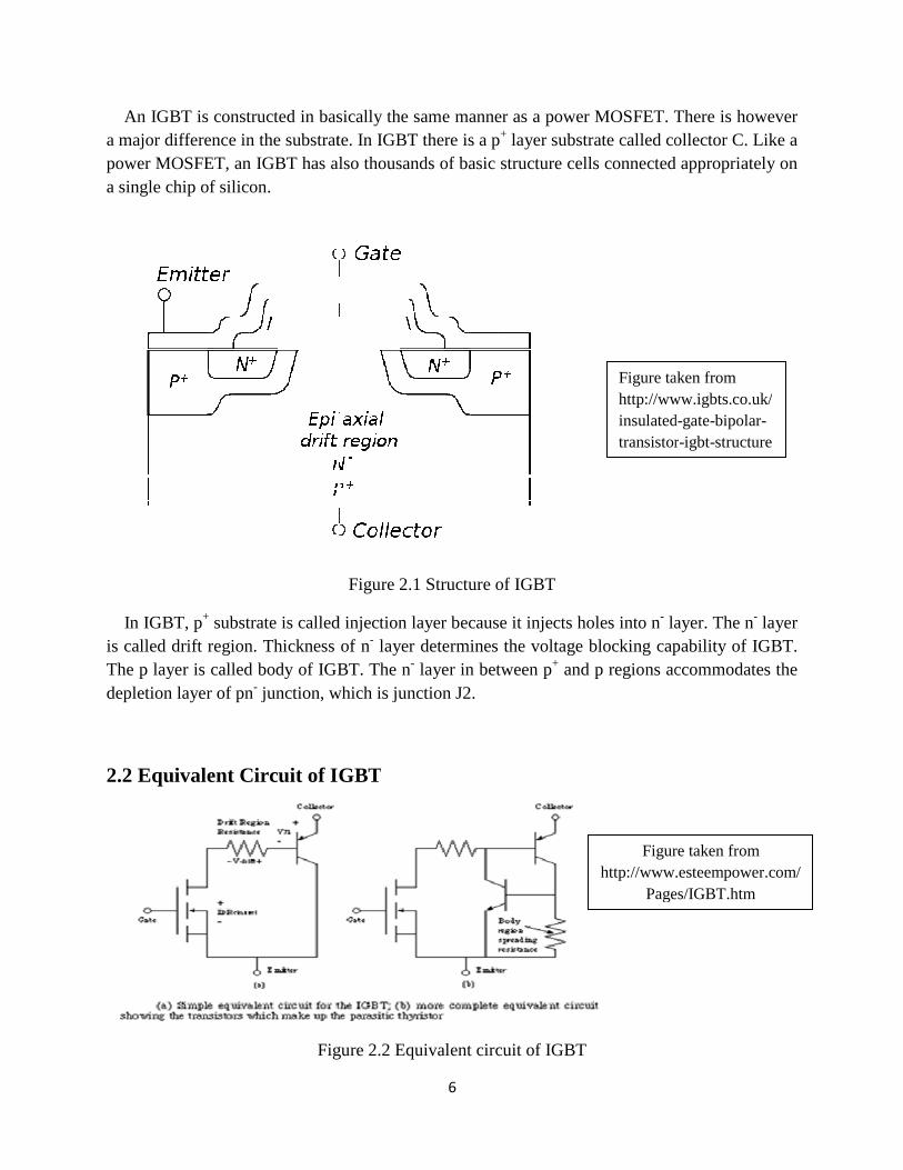
An IGBT is constructed in basically the same manner as a power MOSFET. There is however a major difference in the substrate. In IGBT there is a ppower MOSFET, an IGBT has also thousands of basic structure cells connected aa single chip of silicon.
In IGBT, p+ substrate is called injection layer because it injects holes into nis called drift region. Thickness of nThe p layer is called body of IGBT. The ndepletion layer of pn- junction, which is j
2.2 Equivalent Circuit of IGBT
Figure 2
6
constructed in basically the same manner as a power MOSFET. There is however a major difference in the substrate. In IGBT there is a p+ layer substrate called collector C. Like a power MOSFET, an IGBT has also thousands of basic structure cells connected a
Figure 2.1 Structure of IGBT
substrate is called injection layer because it injects holes into n- layer. The nis called drift region. Thickness of n- layer determines the voltage blocking capability of IGBT. The p layer is called body of IGBT. The n- layer in between p+ and p regions accommodates the
junction, which is junction J2.
of IGBT
Figure 2.2 Equivalent circuit of IGBT
Figure taken from http://www.igbts.co.uk/insulatedtransistor
Figure taken from http://www.esteempower.com/
Pages/IGBT.htm
constructed in basically the same manner as a power MOSFET. There is however layer substrate called collector C. Like a
power MOSFET, an IGBT has also thousands of basic structure cells connected appropriately on
layer. The n- layer layer determines the voltage blocking capability of IGBT.
and p regions accommodates the
Figure taken from http://www.igbts.co.uk/insulated-gate-bipolar-transistor-igbt-structure
Figure taken from http://www.esteempower.com/
Pages/IGBT.htm

7
Referring to the figure, IGBT can be approximately thought of as a combination of a MOSFET and a p+n-p transistor. There is also an n-pn+ transistor formed. There is thus a parasitic thyristor formed by the two transistors p+n-p and n-pn+. Rd is the drift region resistance. Rby is the p-body region resistance.
2.3 Working Principle
When collector is made positive with respect to emitter, IGBT gets forward biased. With no voltage between gate and emitter, the two junctions J2 between n- and p is reverse biased. So no current flows from collector to emitter. When gate is made positive with respect to emitter by a voltage more than the threshold voltage of IGBT, an n-channel or inversion layer is formed in upper part of p-region just below the gate. This n-channel short-circuits the n- and n+ regions. So electrons from n+ region flow into n- region. p+ is already injecting holes into n- region. So the conductivity of n- region increases considerably. IGBT gets turned on and starts conducting forward current IC .
2.4 Latch-up in IGBT
When IGBT is on, hole current flows through transistor p+n-p and p-body resistance Rby. If load current is large, then drop through resistance Rby will be large. This drop will forward bias n-
pn+ transistor. This further facilitates the turn on of p+n-p transistor. This can be a regenerative process. With parasitic thyristor on, IGBT latches up and after this collector current is no longer under the control of gate terminal. The only way now to turn off the latched-up IGBT is by forced commutation of current. If this latch-up isn’t aborted quickly, excessive power dissipation may destroy the IGBT. Hence to avoid this latch-up, collector current mustn’t exceed a certain critical value which must be specified by the manufacturer.
2.5 IGBT characteristics
2.5.1 Static I-V characteristics
Static I-V or output characteristics of an IGBT (n-channel type) show the plot of collector current IC versus collector-emitter voltage VCE for various values of gate-emitter voltages VGE1, VGE2, etc. In the forward direction, the shape of the output characteristics is similar to that of BJT. But here the controlling parameter is VGE as IGBT is a voltage-controlled device. When the device is off, junction J2 blocks forward voltage and in case reverse voltage appears across collector and emitter, J1 blocks it.

Figure 2
2.5.2 Transfer Characteristics
The transfer characteristics of an IGBT is a plot of collector current Ivoltage VGE. This characteristic is identical to that of power MOSFET. When Vthreshold voltage (VGET), the IGBT is in
Figure taken from http://commons.wikimedia.org/wiki/File:IvsV_IGBT.png
8
Figure 2.3 Static I-V characteristics of IGBT
Transfer Characteristics
The transfer characteristics of an IGBT is a plot of collector current IC versus gate. This characteristic is identical to that of power MOSFET. When VGE
IGBT is in off-state.
Figure 2.4 IGBT Transfer Characteristics
Figure taken from http://commons.wikimedia.org/wiki/File:IvsV_IGBT.png
Figure taken from www.semikron.com
versus gate-emitter
GE is less than the
2.4 IGBT Transfer Characteristics
Figure taken from http://commons.wikimedia.org/wiki/File:IvsV_IGBT.png
Figure taken from www.semikron.com

9
2.5.3 Switching Characteristics
The turn-on time is defined as the time between the instants of forward blocking to forward on-state. Turn-on time is composed of delay time tdn and rise time tr, i.e. ton=tdn+tr. The delay time is defined as the time for VCE to fall from VCE to 90% of initial VCE. Time tdn may also be defined as the time for IC to rise from its initial leakage current to 10% of final value of collector current.
The rise time tr is the time during which VCE falls from 0.9 VCE to 0.1 VCE. It is also defined as the time for IC to rise from 0.1 IC to its final value IC. After time ton, collector current is IC, and VCE falls to small value called conduction drop=VCES, where subscript S denotes saturated value.
The turn-off time comprises three intervals:
• Delay time: Time during which gate voltage falls from VGE to threshold voltage VGET. The collector current falls from IC to 0.9 IC. At the end of delay time, VCE begins to rise.
• Initial fall time: Time during which collector current falls from 0.9 to 0.2 of its initial value IC.
• Final fall time: Time during which collector current falls from 0.2 to 0.1 of IC.
Figure 2.5 Switching Characteristics of IGBT
Figure taken from www.semikron.com

10
Chapter 3
BASIC COMPONENTS AND THEIR INTERFACING TECHNIQUES

11
3.1 ATMEGA32L-8PU (AVR Series microcontroller)
3.1.1 Important Features The ATmega32 is a low-power CMOS 8-bit microcontroller based on the AVR enhanced RISC architecture. By executing powerful instructions in a single clock cycle, the ATmega32 achieves throughputs approaching 1 MIPS per MHz allowing the system designer to optimize power consumption versus processing speed.
The important features of ATmega32 are listed below:
• Bytes of In-System Self-Programmable Flash (Endurance: 10,000 Write/Erase Cycles) • 1024 Bytes EEPROM (Endurance: 100,000 Write/Erase Cycles) • 2K Byte Internal SRAM • Two 8-bit Timer/Counters with Separate Prescalers and Compare Modes • One 16-bit Timer/Counter with Separate Prescaler, Compare Mode, and Capture Mode • Four PWM Channels • 8-channel, 10-bit ADC (operated in both single and differential channel mode) • 32 Programmable I/O Lines • Operating Voltages
2.7 - 5.5V for ATmega32L (device operate at 5V DC) 4.5 - 5.5V for ATmega32
• Speed of operation:
0-8MHZ for ATMEGA32L 0-16MHZ for ATMEGA32
• Power Consumption at 1 MHz, 3V, 25°C for ATmega32L
Active: 1.1 mA Idle Mode: 0.35 mA Power-down Mode: less than 1mA.
• Advanced RISC Architecture
131 Powerful Instructions – Most Single-clock Cycle Execution 32 x 8 General Purpose Working Registers Fully Static Operation Up to 16 MIPS Throughput at 16 MHz On-chip 2-cycle Multiplier

12
3.1.2 PIN Configuration
Figure 3.1 PIN Configuration of Atmega32 Microcontroller
ATMEGA32 MICROCONTROLLER (Figure taken from ATMEGA32 datasheet, ATMEL CORP.)
13
3.1.3 Programming AVR Microcontroller C language is used for programming AVR microcontroller. First requirement is a compiler, which is required to convert C code to machine code (Hex code), which is ultimately transferred to flash memory of microcontroller. I have used WINAVR2006 compiler. The second requirement is a programmer which transfers the .hex file (created by the compiler) to the chip. BSD programmer is used for that. AVRDUDE software is used for programming ATMEGA32 CPU.
3.1.4 Installation of WINAVR Software WINAVR2006 compiler is installed in PC C drive. install_giveio.bat (inside winavr/bin directories) file is executed to access parallel port of computer. One C file and one make file is required to generate hex code for AVR microcontrollers. Make file specifies the device (microcontroller) name, frequency of operation, output code format, programmer type, and PC port which is connected to the programmer etc. to the compiler. One make file editor and one .C file editor is located on desktop. One make file of a specific format is stored in the same folder where the .C file is created.
3.1.5 MAKEFILE Specifications The following changes have been done in makefile editor to create makefile for ATMEGA32 microcontroller.
• MCU type – ATMEGA32 • PROGRAMMER – BSD • PORT - LPT PORT • DEBUGGER- AVR-EXT-COFF(AVRSTUDIO 4.07+, VMLAB 3.10+) • TARGET- main.c (same as .c file name)
3.1.6 Installation of AVRDUDE AVRDUDE is a full featured FreeBSD UNIX program for programming Atmel's AVR CPU's. It can program the Flash and EEPROM, and where supported by the serial programming protocol, it can program fuse and lock bits. AVRDUDE can be used effectively via the command line to read or write all chip memory types (EEPROM, flash, fuse bits, lock bits, signature bytes) or via an interactive (terminal) mode.

14
AVRDUDE software is installed in same drive in which WINAVR compiler is installed. WINAVR compiler internally use AVRDUDE programmer to transfer .hex file to microcontroller.
3.2 Components used
Serial number Component Quantity
1. Diode(SB560) 5 2. IGBT(IRG4PC30U) 1 3. Atmega32 Microcontroller 1 4. Potentiometer(100K) 1 5. Comparator (LM324) 1 6. 1-phase Transformer(230V/6V,1Amp) 1 7. Crystal Oscillator(6.5536MHz) 1 8. Constant Voltage Regulator(L7805) 1 9. DC Li ion battery(2000ma-hr,3.8V) 2
3.3 Softwares used
1. Multisim (Student Version 10.1, National Instruments) – Used for simulation purpose. 2. Diptrace (Evaluation Version 1.5) – Used for circuit layout design. 3. WinAvr compiler (Version 2.0.6.1) – Used as a C language compiler for Atmega32
microcontroller. 4. MATLAB and Simulink

3.4 Operation of the converter
3.4.1 Basic Function
A bridge rectifier configurationAC input of 230V, 50Hz supplythe full-wave bridge serves to convert an AC input into a DC output, the addition of a capacitor is be desired because the bridge alone supplies an output of fixed polarity but continuously varying or pulsating magnitude
Figure 3.2 Graetz Bridge and smoothing capacitor
The function of this capacitor, known asthe variation in (or 'smooth') the rectified AC outputexplanation of smoothing is that the capacitor provides a low impedance path to the AC component of the output, reducing the AC voltage across, and AC current through, the resistive load. In less technical terms, any canceled by loss of charge in the capacitor. This charge flows out as additional current through the load. Thus the change of load current and voltage is reduced relative to what would occur without the capacitor. Increases of voltage correspondingly store excess charge in the capacitor, thus moderating the change in output voltage/current.
Figure taken from http://en.wikipedia.org/wiki/Diode_bridge
15
of the converter
configuration (Graetz Bridge) of four diodes (IN5406) is used 50Hz supply. For many applications, especially with single phase AC where
wave bridge serves to convert an AC input into a DC output, the addition of be desired because the bridge alone supplies an output of fixed polarity but
pulsating magnitude.
Figure 3.2 Graetz Bridge and smoothing capacitor
The function of this capacitor, known as reservoir capacitor or smoothing capacitor is to lessen the variation in (or 'smooth') the rectified AC output voltage waveform from the bridge. One explanation of smoothing is that the capacitor provides a low impedance path to the AC component of the output, reducing the AC voltage across, and AC current through, the resistive load. In less technical terms, any drop in the output voltage and current of the bridge tends to be canceled by loss of charge in the capacitor. This charge flows out as additional current through the load. Thus the change of load current and voltage is reduced relative to what would occur without the capacitor. Increases of voltage correspondingly store excess charge in the capacitor, thus moderating the change in output voltage/current.
Reservoir Capacitor or Smoothing Capacitor
Figure taken from http://en.wikipedia.org/wiki/Diode_bridge
used to rectify the For many applications, especially with single phase AC where
wave bridge serves to convert an AC input into a DC output, the addition of be desired because the bridge alone supplies an output of fixed polarity but
or smoothing capacitor is to lessen voltage waveform from the bridge. One
explanation of smoothing is that the capacitor provides a low impedance path to the AC component of the output, reducing the AC voltage across, and AC current through, the resistive
drop in the output voltage and current of the bridge tends to be canceled by loss of charge in the capacitor. This charge flows out as additional current through the load. Thus the change of load current and voltage is reduced relative to what would occur without the capacitor. Increases of voltage correspondingly store excess charge in the capacitor,

16
The rectified AC is fed to the IGBT. To control the output DC voltage multipulse PWM (here 8-pulse) method is used, which varies the duty cycle of the IGBT. Different duty cycle value of PWM is used to control the switching of IGBT (IRG4PC30U) by which the average voltage or average time of power delivery from the source is controlled.
A pulse of constant frequency (400HZ) of adjustable duty cycle is generated using ATMEGA32 microcontroller (AVR series) in fast PWM mode. To produce a PWM two counters are used: one counter attributes to frequency of the PWM and the value of other counter is set to adjust the duty cycle. Across the load a freewheeling diode is connected which comes into play in case of inductive load.
3.4.2 Voltage Control by the Knob
A knob is used for the user to control the voltage level. This knob is a potentiometer of value 100K. A voltage supply of 5V is applied across it and the middle terminal is connected to one of the input of the ADC channel at PORT A of the microcontroller. The ADC is operated at reference value 5V (constant) and resolution of 10bit (0.005V) in comparator mode. The duty cycle of the PWM is determined from the corresponding ADC value for a particular knob position.

3.4.3 Circuit Schematic
Assembling the components described above in the Diptrace software, we build the following circuit schematic of the AC to DC
Figure 3.3 Circuit diagram of an AC to DC converter using microcontroller
17
Assembling the components described above in the Diptrace software, we build the following AC to DC converter.
Figure 3.3 Circuit diagram of an AC to DC converter using microcontroller (Designed using DIPTRACE software)
Assembling the components described above in the Diptrace software, we build the following
(Designed using

18
Chapter 4
SIMULATION IN MULTISIM (N.I.)

4.1 Simulation Circuit Diagra
The complete simulation is carried outgiven below:
Figure 4.1 Simulation circuit in Multisim
19
Diagram
The complete simulation is carried out using Multisim software. The simulation diagram is
Figure 4.1 Simulation circuit in Multisim
using Multisim software. The simulation diagram is

4.2 Simulation Results
Simulations for different load conditions and different dutyMultisim (Student Version) software.
Scale: X axis: 1 big division = 5 milliseconds
Y axis: 1 big division = 200V
Result 1- (for a load of 1K-ohms and duty cycle 90%)
Result 2- (for a load of 1K-ohms
Voltage
Voltage
20
Simulations for different load conditions and different duty-cycles are carried out by using Multisim (Student Version) software. The waveforms are of output voltage and gate signals.
: X axis: 1 big division = 5 milliseconds
Y axis: 1 big division = 200V
ohms and duty cycle 90%)
ohms and duty cycle 60%)
Time
Time
Figure 4.2
Figure 4.3
cycles are carried out by using The waveforms are of output voltage and gate signals.
Output voltage
Gate signal

Result 3- (for a load of 1K-ohms
Result 4- (for a load of 500 ohms
Voltage
Voltage
21
ohms and duty cycle 30%)
500 ohms and duty cycle 90%)
Time
Time
Figure 4.5
Figure 4.4
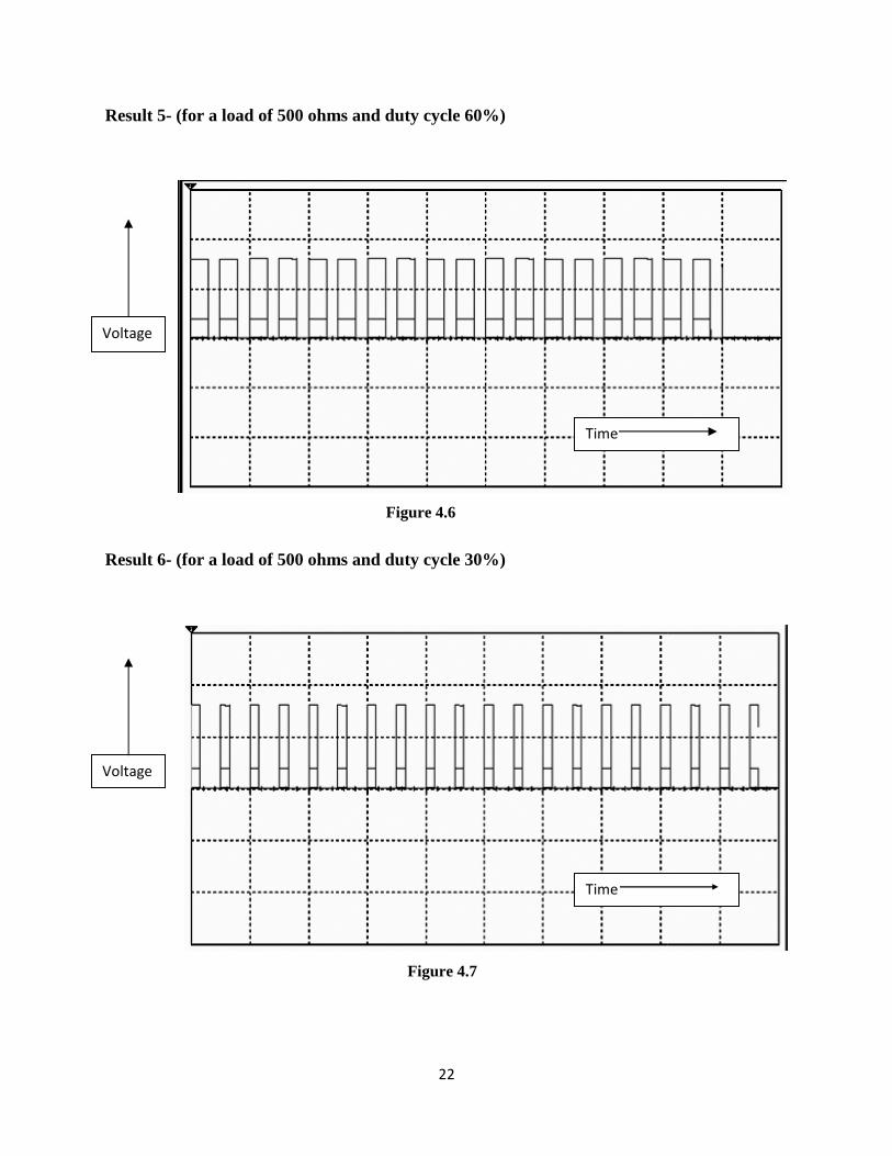
Result 5- (for a load of 500 ohms
Result 6- (for a load of 500 ohms
Voltage
Voltage
22
ohms and duty cycle 60%)
500 ohms and duty cycle 30%)
Time
Time
Figure 4.6
Figure 4.7
23
Chapter 5
VOLTAGE CONTROL USING PID
ALGORITHM

24
The PID algorithm is the most popular feedback controller used within the process industries. It has been successfully used for over 50 years. It is a robust and easily understood algorithm that can provide excellent control performance despite the varied dynamic characteristics of process plant.
5.1 The Proportional-Integral-Derivative (PID) algorithm
As the name suggests, the PID algorithm consists of three basic modes, the Proportional, the Integral and the Derivative modes. When utilizing this algorithm it is necessary to decide which modes are to be used (which combinations of P, I and D?) and then specify the parameters (or settings) for each mode used. Generally, three basic algorithms are used P, PI or PID.
5.1.1 A Proportional algorithm
The mathematical representation is,
(Laplace domain)
or . (time domain)
The proportional mode adjusts the output signal in direct proportion to the controller input (which is the error signal, e). The adjustable parameter to be specified is the controller gain, kc. This is not to be confused with the process gain, kp. The larger kc the more the controller output will change for a given error. For instance, with a gain of 1 an error of 10% of scale will change the controller output by 10% of scale. Many instrument manufacturers use Proportional Band (PB) instead of kc.

25
The time domain expression also indicates that the controller requires calibration around the steady-state operating point. This is indicated by the constant term . This represents the 'steady-state' signal for the mv and is used to ensure that at zero error the cv is at set point. In the Laplace domain this term disappears, because of the ‘deviation variable’ representation.
A proportional controller reduces error but does not eliminate it (unless the process has naturally integrating properties), i.e. an offset between the actual and desired value will normally exist.
5.1.2 A proportional integral algorithm
The mathematical representation is,
or !" #$%
& !'
The additional integral mode (often referred to as reset) corrects for any offset (error) that may occur between the desired value (set point) and the process output automatically over time. The adjustable parameter to be specified is the integral time (Ti) of the controller.
5.1.3 A Proportional Integral Derivative algorithm
The mathematical representation is,
(
or )* = m) +*
& +*,* (,+*
,*

Derivative action (also called rate or prelooking at the time rate of change of the controlled variable (its derivative). TD is the ‘rate time’ and this characterizes the derivative action (with units of minutes). In theory derivative action should always improve dynamic respproblem of noisy signals makes the use of derivative action undesirable (differentiating noisy signals can translate into excessive mv movement). Derivative action depends on the slope of the error, unlike P and I. If the error is constant derivative action has no effect.
5.2 The characteristics of P, I
Figure 5.1 Block diagram of a plant with a controller Plant: A system to be controlledController : Provides the excitation to
A proportional controller (Kp) will have the effect of reducing the rise time and will reduce, but never eliminate, the steadyeliminating the steady-state error, but it may make the transient response worse. A derivative control (Kd) will have the effect of increasing the stability of the system, reand improving the transient response. Effects of each of controllers Kp, Kd, and Ki on a closedloop system are summarized in the table shown below.
CL RESPONSE RISE TIME
Kp Decrease
Ki Decrease
Kd Small Change
26
Derivative action (also called rate or pre-act) anticipates where the process is heading by looking at the time rate of change of the controlled variable (its derivative). TD is the ‘rate time’ and this characterizes the derivative action (with units of minutes). In theory derivative action should always improve dynamic response and it does in many loops. In others, however, the problem of noisy signals makes the use of derivative action undesirable (differentiating noisy signals can translate into excessive mv movement). Derivative action depends on the slope of the
nlike P and I. If the error is constant derivative action has no effect.
5.2 The characteristics of P, I and D controllers
Figure 5.1 Block diagram of a plant with a controller
be controlled. excitation to the plant; designed to control the overall system behavior
A proportional controller (Kp) will have the effect of reducing the rise time and will reduce, steady-state error. An integral control (Ki) will have the effect of
state error, but it may make the transient response worse. A derivative control (Kd) will have the effect of increasing the stability of the system, reducing the overshoot, and improving the transient response. Effects of each of controllers Kp, Kd, and Ki on a closedloop system are summarized in the table shown below.
OVERSHOOT SETTLING TIME S
Increase Small Change
Increase Increase
Small Change Decrease Decrease Small Change
process is heading by looking at the time rate of change of the controlled variable (its derivative). TD is the ‘rate time’ and this characterizes the derivative action (with units of minutes). In theory derivative action
onse and it does in many loops. In others, however, the problem of noisy signals makes the use of derivative action undesirable (differentiating noisy signals can translate into excessive mv movement). Derivative action depends on the slope of the
esigned to control the overall system behavior.
A proportional controller (Kp) will have the effect of reducing the rise time and will reduce, . An integral control (Ki) will have the effect of
state error, but it may make the transient response worse. A derivative ducing the overshoot,
and improving the transient response. Effects of each of controllers Kp, Kd, and Ki on a closed-
S-S ERROR
Decrease
Eliminate
Small Change
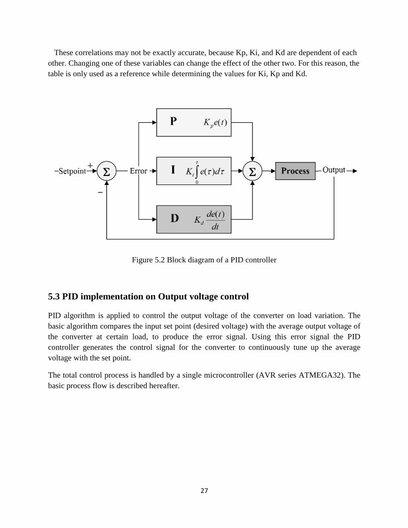
These correlations may not be exactly accurate, because Kp, Ki, and Kd are dependent of each other. Changing one of these variables can change the effect of the other two. For this reason, the table is only used as a reference while determining the values
Figure 5.2 Block diagram of a PID controller
5.3 PID implementation on Output voltage control PID algorithm is applied to control the output voltage of the converter on load variation. The basic algorithm compares the input set the converter at certain load, to produce the error signal. Using this error signal the PID controller generates the control signal for the converter to continuously tune up the average voltage with the set point.
The total control process is handled by a single microcontroller (AVR series ATMEGA32). basic process flow is described hereafter
27
These correlations may not be exactly accurate, because Kp, Ki, and Kd are dependent of each other. Changing one of these variables can change the effect of the other two. For this reason, the table is only used as a reference while determining the values for Ki, Kp and Kd.
Figure 5.2 Block diagram of a PID controller
PID implementation on Output voltage control
PID algorithm is applied to control the output voltage of the converter on load variation. The basic algorithm compares the input set point (desired voltage) with the average output voltage of the converter at certain load, to produce the error signal. Using this error signal the PID controller generates the control signal for the converter to continuously tune up the average
The total control process is handled by a single microcontroller (AVR series ATMEGA32). process flow is described hereafter.
These correlations may not be exactly accurate, because Kp, Ki, and Kd are dependent of each other. Changing one of these variables can change the effect of the other two. For this reason, the
for Ki, Kp and Kd.
PID algorithm is applied to control the output voltage of the converter on load variation. The point (desired voltage) with the average output voltage of
the converter at certain load, to produce the error signal. Using this error signal the PID controller generates the control signal for the converter to continuously tune up the average
The total control process is handled by a single microcontroller (AVR series ATMEGA32). The

5.3.1 Determination of Average output voltage
The maximum DC output voltage is supply. If the duty cycle is ‘D’ then the average voltage is 325*D. The microcontroller can only handle voltage upto 5V. Hence the output voltage at the converter end has to be first scaled down to a range in between 0V to 5V.This is achieved using a potentiometer of high resistance value (1MΩ), in order to reduce losses.
Figure 5.3 Measurement of output voltage by microcontroller
Analysis of the above figure shows that for D=1 (mathe transformation ratio is 325/5=65. So the input voltage to microcontroller ADC channel has to be multiplied by 65 to get the corresponding output voltage of the converter.
The different values of the output voltage 2.5 milliseconds (1/400Hz). After getting all those values for a cycle the average voltagecalculated and scaled up by a factor of 65.
5.3.2 PID implementation
The error in the voltage is calculated by comparing the average output voltage Vo and set point voltage Vset. This is given as
28
Determination of Average output voltage
The maximum DC output voltage is equal to 230* = 325V for single phase 230V AC power supply. If the duty cycle is ‘D’ then the average voltage is 325*D. The microcontroller can only handle voltage upto 5V. Hence the output voltage at the converter end has to be first scaled down
0V to 5V.This is achieved using a potentiometer of high resistance value ), in order to reduce losses.
Figure 5.3 Measurement of output voltage by microcontroller
Analysis of the above figure shows that for D=1 (maximum value), the input voltage is 5V. So the transformation ratio is 325/5=65. So the input voltage to microcontroller ADC channel has to be multiplied by 65 to get the corresponding output voltage of the converter.
The different values of the output voltage are stored in the microcontroller for a time period of 2.5 milliseconds (1/400Hz). After getting all those values for a cycle the average voltagecalculated and scaled up by a factor of 65.
The error in the voltage is calculated by comparing the average output voltage Vo and set point
= 325V for single phase 230V AC power supply. If the duty cycle is ‘D’ then the average voltage is 325*D. The microcontroller can only handle voltage upto 5V. Hence the output voltage at the converter end has to be first scaled down
0V to 5V.This is achieved using a potentiometer of high resistance value
ximum value), the input voltage is 5V. So the transformation ratio is 325/5=65. So the input voltage to microcontroller ADC channel has to
are stored in the microcontroller for a time period of 2.5 milliseconds (1/400Hz). After getting all those values for a cycle the average voltage Vo is
The error in the voltage is calculated by comparing the average output voltage Vo and set point
To microcontroller ADC channel

e(t)= Vset(t)
After getting the error signal, the PID algorithm is applied to generate necessaryfor the plant. The input to the plant is generated by processing the error signal and hence the desired voltage is achieved by adjusting the duty cycle of the gate pulse to the IGBT.
5.3.3 The Plant Model
The converter including the source can be modeled as shown in figure.
Let V1= source dc voltage, VL = voltage across the load, Rs = source resistance
The transfer function of the open loop gain is found as:
29
e(t)= Vset(t) – Vo(t)
After getting the error signal, the PID algorithm is applied to generate necessaryfor the plant. The input to the plant is generated by processing the error signal and hence the desired voltage is achieved by adjusting the duty cycle of the gate pulse to the IGBT.
source can be modeled as shown in figure.
Figure 5.4 Plant Model
= voltage across the load, Rs = source resistance
The transfer function of the open loop gain is found as:
After getting the error signal, the PID algorithm is applied to generate necessary control action for the plant. The input to the plant is generated by processing the error signal and hence the desired voltage is achieved by adjusting the duty cycle of the gate pulse to the IGBT.

The open loop response of the model, obtained by The response shows that, the output voltage never reaches the same as the input voltage.
MATLAB program
clc;
clear all;
close all;
E0=1;
rs=1;rl=50;L=0.015,C=10^(
num=[ rl];
den=[ rs*L*C rl*rs*C+L rl+rs];
u=20/E0;
step(u*num,den);
30
The open loop response of the model, obtained by Matlab, to step input of 20V is shown below. The response shows that, the output voltage never reaches the same as the input voltage.
Figure 5.5 Open loop response
;rl=50;L=0.015,C=10^(-3);
num=[ rl];
den=[ rs*L*C rl*rs*C+L rl+rs];
step(u*num,den);
Matlab, to step input of 20V is shown below. The response shows that, the output voltage never reaches the same as the input voltage.

5.3.4 Proportional Integral Derivative
The close loop transfer function (G) ,in laplace domain,of the model including the PID controller is given as follows.
Where Kp = Proportional gain
Kd= Derivative gain
Ki= Integral gain
5.3.5 Application of Proportional control
Applying proportional control only we get the following response for a voltage variation of 20V, due to load change. Here Kp = 50, K
Figure 5.6 Response
31
Integral Derivative control (PID)
The close loop transfer function (G) ,in laplace domain,of the model including the PID controller
Application of Proportional control (P)
Applying proportional control only we get the following response for a voltage variation of 20V, = 50, Kd=0, Ki=0
Figure 5.6 Response due to proportional control
The close loop transfer function (G) ,in laplace domain,of the model including the PID controller
Applying proportional control only we get the following response for a voltage variation of 20V,

MATLAB program
kp=50;
ki=0;
kd=0;
num2=[ kd*rl kp*rl ki*rl];
den2=[ rs*L*C rl*rs*C+L+kd*rl rl+rs+kp*rl ki*rl];
figure;
t=0:0.0001:0.05;
step(u*num2,den2,t);
5.3.6 Application of Proportional
Applying Proportional-Integral control we get the following response for a voltage 20V, due to load change. Here K
Figure 5.7 Response due to P
32
num2=[ kd*rl kp*rl ki*rl];
den2=[ rs*L*C rl*rs*C+L+kd*rl rl+rs+kp*rl ki*rl];
t=0:0.0001:0.05;
step(u*num2,den2,t);
Application of Proportional Integral control (PI)
Integral control we get the following response for a voltage Here Kp = 50, Kd=0, Ki=200
Figure 5.7 Response due to P-I control
Integral control we get the following response for a voltage variation of

MATLAB program
kp=50;
ki=200;
kd=0;
num2=[ kd*rl kp*rl ki*rl];
den2=[ rs*L*C rl*rs*C+L+kd*rl rl+rs+kp*rl ki*rl];
figure;
t=0:0.0001:0.1;
step(u*num2,den2,t);
5.3.7 Application of Proportional
Applying Proportional-Integral-Derivative control we get the following response for a voltage variation of 20V, due to load change
Figure 5.8 Response due to P
33
num2=[ kd*rl kp*rl ki*rl];
den2=[ rs*L*C rl*rs*C+L+kd*rl rl+rs+kp*rl ki*rl];
t=0:0.0001:0.1;
step(u*num2,den2,t);
Application of Proportional -Integral-Derivative control (PID)
Derivative control we get the following response for a voltage due to load change. Here Kp = 50, Kd=0.03, Ki=200
Figure 5.8 Response due to P-I-D control
Derivative control we get the following response for a voltage
34
MATLAB program
kp=50;
ki=200;
kd=0.03;
num2=[ kd*rl kp*rl ki*rl];
den2=[ rs*L*C rl*rs*C+L+kd*rl rl+rs+kp*rl ki*rl];
figure;
t=0:0.0001:0.5;
step(u*num2,den2,t);
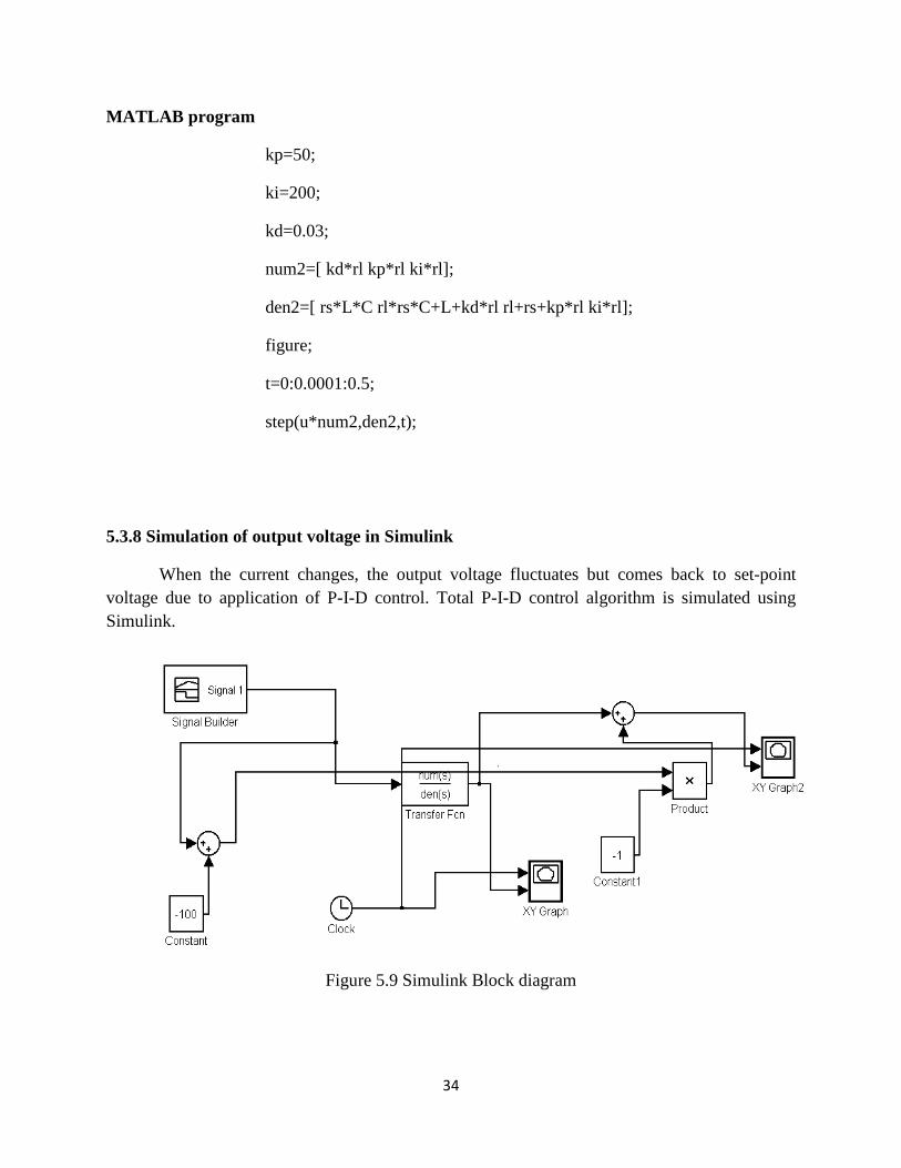
5.3.8 Simulation of output voltage in Simulink
When the current changes, the output voltage fluctuates but comes back to set-point voltage due to application of P-I-D control. Total P-I-D control algorithm is simulated using Simulink.
Figure 5.9 Simulink Block diagram

The graphs showing the load voltage variation with Pbelow. are shown below.
Figure 5.10 Voltage variation
Figure 5.11
VOLTAGE
VOLTAGE
35
The graphs showing the load voltage variation with P-I-D control and without control is shown
Voltage variation due to load change without control
Figure 5.11 Voltage variation with P-I-D control Time
control and without control is shown
without control
Time

5.3.9 Load resistance measurement
Figure 5.12
Design is being done for the maximum load current resistance (0.5Ω) is 15V (maximum). This voltage is scaled down by the potentiometer of 1Mto a range of 0V to 5V, in order to make it compatible with the microcontroller,using the differential channel of the microcontrollerdetermined. Now dividing the load voltage by the load curren
36
Load resistance measurement
Figure 5.12 Calculation of load resistance
Design is being done for the maximum load current of 30A. Hence the drop across the (maximum). This voltage is scaled down by the potentiometer of 1M
to a range of 0V to 5V, in order to make it compatible with the microcontroller, using the differential channel of the microcontroller. Hence load current in the circuit is
Now dividing the load voltage by the load current the load resistance is determined.
. Hence the drop across the test (maximum). This voltage is scaled down by the potentiometer of 1MΩ
and measured by Hence load current in the circuit is
load resistance is determined.
Differential
channel of the
microcontroller

37
5.3.10 Voltage control across the load due to AC voltage fluctuation
Maximum DC voltage is given as : Vdc,mx= Vrms/ac *√2 =230*1.414= 325.27V
Average voltage across the load is given as: VL = D* Vdc,mx
Where D = duty cycle of the gate pulse
Vdc,mx is calculated by scaling down the voltage at the rectifier end by a 1MΩ potentiometer to a voltage range of 0v to 5v range, in order to make it compatible with the microcontroller, and connected to the ADC channel(PA3 pin) of ATNEGA32. For a given output load voltage(VL) the ratio between VL and Vdc,mx , which is same as the duty cycle, is calculated and the is change d to the new calculated value to maintain the constant set-point voltage across the load.
The microcontroller is programmed to work for certain tolerance limit of AC voltage fluctuation, beyond which the circuit is isolated by switching of the gate pulse.

38
CONCLUSION

39
We draw the following conclusions
1. We have performed the simulation work and could able to vary the average voltage using 2. PWM technique with a low fluctuation. 3. IGBTs possess many desirable properties including high switching speed, low conduction
voltage drop, high current carrying capability, and a high degree of robustness. 4. The availability of IGBTs lowers the cost of systems and enhances the number of
economically viable applications. 5. The insulated gate bipolar transistor (IGBT) combines the positive attributes of BJTs and
MOSFETs. BJTs have lower conduction losses in the on-state, especially in devices with larger blocking voltages, but have longer switching times, especially at turn-off while MOSFETs can be turned on and off much faster, but their on-state conduction losses are larger, especially in devices rated for higher blocking voltages. Hence, IGBTs have lower on-state voltage drop with high blocking voltage capabilities in addition to fast switching speeds.
6. By varying the duty cycle of the gate pulse of IGBT, the output voltage was effectively varied.
7. By use of multipulse triggering, the harmonics were significantly reduced. 8. When load varies, the output voltage fluctuates. So PID control algorithm is used. 9. In proportional control error is reduced but can’t be eliminated. In P-I control error is
completely eliminated after certain time, but overshoot is increased. In P-I-D control, due to derivative gain, the overshoot is minimized.

40
REFERENCES

41
1. Bimbhra , Dr. P.S., Power Electronics ,Khanna Publishers, 2
2. Rashid, Muhammad H., Power Electronics. New Delhi: Prentice Hall of India Pvt Ltd 2001.
3. Skibinski, G. Maslowski, W. Pankau, J. ;Installation considerations for IGBT AC
drives;Textile, Fiber, and Film Industry Technical Conference, 1997., IEEE 1997 Annual;May 1997 (http://ieeexplore.ieee.org/stamp/stamp.jsp?tp=&arnumber=598530&isnumber=13056)
4. ATMEGA32 Datasheet , ATMEL Corporation.
5. www.NI.com
6. www.atmel.com
7. http://www.engin.umich.edu/group/ctm/PID/PID.html#introduction ,
Carnigie Mellon University