DEVELOPMENT AND APPLICATION OF GENERAL CIRCUIT THEORY...
149
DEVELOPMENT AND APPLICATION OF GENERAL CIRCUIT THEORY TO SUPPORT CAPACITIVE COUPLING Yusuf Mahomed A dissertation submitted to the Faculty of Engineering and the Built Environment, University of Witwatersrand, Johannesburg, in fulfilment of the requirements for the degree of Master of Science in Engineering. Johannesburg, 2011
-
Upload
trinhnguyet -
Category
Documents
-
view
218 -
download
1
Transcript of DEVELOPMENT AND APPLICATION OF GENERAL CIRCUIT THEORY...

DEVELOPMENT AND APPLICATION OF
GENERAL CIRCUIT THEORY TO
SUPPORT CAPACITIVE COUPLING
Yusuf Mahomed
A dissertation submitted to the Faculty of Engineering and the Built Environment,
University of Witwatersrand, Johannesburg, in fulfilment of the requirements for
the degree of Master of Science in Engineering.
Johannesburg, 2011

i
Declaration
I declare that this dissertation is my own unaided work. It is being submitted to
the degree of Master of Science in Engineering at the University of the
Witwatersrand, Johannesburg. It has not been submitted before for any degree or
examination at any other university.
_________________________________
Signed on: ____ day of _________ 20___

ii
Abstract
In textbook literature, the phenomenon of mutual inductance has been described in
rigorous detail from the magnetic field-level behaviour all the way to equivalent circuit
models, and these are valid for circuits consisting of any number of coils where there
may be magnetic flux linkage. Unlike mutual inductance, the description of multi-body
systems which exhibit electric flux coupling has not been carried through from a field
level to equivalent circuit models in the same way. Most circuit models used to
describe capacitive coupling are therefore different and cannot be easily compared.
In this dissertation, a general circuit model describing capacitive coupling is developed
from field-level theory. This model is based on a four-body physical structure, and
forms a restricted dual to the well-known two-body inductive coupling circuit model.
A quantity representing coupling capacitance was defined and given the symbol S, and
this quantity is the dual to the mutual inductance term commonly referred to by the
symbol M in textbook literature. An in-depth analysis is documented into the coupling
capacitance term S, showing that it is possible to obtain a system which exhibits
positive, negative or zero coupling. Experimental verification was done for systems
exhibiting zero coupling, 100 % coupling and arbitrary coupling. For all cases, the
experimental results had very good agreement to the values predicted using the
capacitive coupling circuit model.
The circuit properties of the capacitive coupling model hold in the same way as it does
for inductive coupling, as expected of a dual model. In general, interconnections of
capacitive coupled networks can also be made as long as specific conditions are met.
A concise discussion into different possible practical applications of the circuit model
is then provided, together with circuit diagrams. This is followed by a detailed
discussion into a condition-monitoring application for inductive (power) transformers.
It is shown theoretically and experimentally that the capacitive coupling circuit model
can be used in condition-monitoring of power transformers to detect mechanical
movements of coils.
The dissertation is concluded with a discussion on possible future work.

iii
Opsomming
Die verskynsel van onderlingeinduktansie is al breedvoerig in die literatuur beskryf
vanuit beide die veldteorie sowel as ekwivalente stroombaanmodelle. Hierdie
stroombaanmodelle is geldig vir enige aantal spoele waar daar gemeenskaplike
magnetiesevloedkoppeling voorkom. In teenstelling hiermee is daar geen soortgelyke
beskrywing van die elektriesevloedkoppeling van veelliggaamstelsels waar die
veldteorie deurgetrek word na die stroombaan model nie. Die meeste
stroombaanmodelle wat gebruik word om kapasitiewe koppeling te beskryf verskil en
dit is dus moeilik om verskillende stelsels te vergelyk.
In hierdie verhandeling word ʼn ekwivalente stroombaanmodel wat kapasitiewe
koppeling beskryf vanuit veldteorie afgelei. Hierdie model is gebaseer op ʼn
vierliggaam- fisiese struktuur. Vanuit ʼn terminale perspektief vorm dit ʼn sogenaamde
beperkte dualis van die welbekende onderlingeinduktansie stroombaan model met
twee spoele (liggame). ʼn Grootheid wat die koppelingkapasitasie verteenwoordig is
gedefinieer en word die simbool S gegee. Hierdie grootheid is tweeledig tot die
onderlingeinduktansieterm wat in teksboekliteratuur algemeen deur die simbool M
voorgestel word. ʼn Diepgaande ontleding van die koppelingkapsitasiesterm S, is
gedokumenteer en toon aan dat dit moontlik is om 'n stelsel wat positiewe, negatiewe
of nul-koppeling toon te verkry. Eksperimentele verifikasie is gedoen vir stelsels wat
nul-koppeling, 100 %-koppeling en arbitrêre koppeling vertoon. Deur gebruik te maak
van die kapasitiewekoppeling-stroombaanmodel het die eksperimentele uitslae in al die
gevalle baie goed ooreengestem met die voorspelde waardes .
Die stroombaaneienskappe van die kapasitiewekoppelingmodel is soortgelyk aan die
vir induktiewekoppeling, soos verwag sou word van ʼn dualis. Interverbindings van
kapasitief-gekoppelde netwerke is ook moontlik solank bepaalde toestande geld.
ʼn Bondige bespreking van verskillende moontlike werklike toepassings van die
stroombaanmodel word vervolgens gegee, tesame met stroombaandiagramme. Dit
word gevolg deur ʼn dieper bespreking van ʼn kondisie-monitering toepassing vir
induktiewe (krag-) transformators. Die verhandeling sluit af met ʼn bespreking van
moontlike toekomstige werk.

iv
ملخص
ان ظاھرة الحث المتبادل مفھومة على نطاق واسع وموثقة في الكتب المنھجية بشكل جيد. فقد وصفت بتفصيل دقيق من
سلوك مستوى المجال المغناطيسي الى النماذج المعادلة للدوائر وھي دقيقة للدوائر التي تتكون من أي كمية من الملفات
لتدفق المغناطيسي.التي من الممكن ان تكون في توصيل ا
ومشابھا للحث المتبادل، فان نظم اHجسام المتعددة التي تعرض ربط التدفق الكھربائي قد وصفت بشكل دقيق على
مستوى المجال اH ان ھذا الوصف لم يتم من خMل وصف مستوى المجال المغناطيسي مرورا بالنماذج المعادلة
رة الحث المتبادل. ھذا يعني: اوH، ان معظم النماذج المعادلة للدوائر للدوائر كما ھي الحالة التي وصفت بھا ظاھ
الموظفة من اجل وصف الربط السعوي مختلفة، وبالتالي فانه من الصعب مقارنة انظمة مختلفة معتمدا على نفس
النموذج. ثانيا، ان العMقة ما بين نموذج الدائرة ومستوى نشاط المجال غير واضح أحيانا.
ذه اZطروحة، ان النموذج المعادل للدائرة والذي يصف الربط السعوي سوف يستخلص من نظرية مستوى في ھ
المجال. ويستند ھذا النموذج على ھيكل فيزيائي رباعي، ويشكل ثنائية معروفة للجسمين الحثيين المربوطين بنموذج
، وھذه الكمية ھي ثنائية Sواعطيت الرمز الدائرة من منظور الربط النھائي. وقد عرفت كمية تمثل الربط السعوي
في الكتب المنھجية. Mلمصطلح الحث المتبادل ويشار اليھا عادة بالرمز
يمكن ان يعرض ربط ، مبينا أنه من الممكن الحصول على نظام Sوقد تم توثيق تحليل معمق لمصطلح الربط السعوي
H يوجد ايجابي او سلبي او منعدم. كذلك تم اظھار انه وبسبب العزل الكھربائي الواضح بين روابط ا^دخال وا^خراج
%، او 100. وقد تم التحقق من تجريبية اZنظمة التي تعرض ربط منعدم، او ربط Sأھمية لaشارة بمفھوم المصطلح
فإن النتائج التجريبية متفقة بشكل جيد للغاية مع القيم المتنبأ بھا عند استخدام نموذج ربط متراوح. وفي جميع الحاHت،
الربط السعوي للدائرة.
وقد تم استكشاف خصائص دائرة الربط السعوي ووجدت بانھا تعمل بنفس الطريقة التي تعمل في الربط الحثي كما ھو
ان عملية الربط السعوي للشبكات ممكنة بتوافر شروط معينة.متوقع من النموذج الثنائي. وبشكل عام تم الكشف عن
كما تم التزويد بمناقشة موجزة عن مختلف التطبيقات التجريبية الممكنة لنموذج الدائرة وبمخططات نموذج الدائرة.
نموذج واعقب ھذا منقاشة تفصيلية تدور حول شروط تطبيق رصد المحوHت (القوى) الحثية. وثبت نظريا ومخبريا ان
الربط السعوي للدائرة يمكن ان يستخدم في شروط رصد محوHت القوى للتحري حركات مكانيكية للملفات.
وختمت اZطروحة بمناقشة حول اHعمال المحتملة في المستقبل.

v
Acknowledgements
The author would like to thank his parents for their unwavering support and motivation, his
supervisor for always being available to help and his friends who provided worthwhile
distractions throughout the course of his studies.

vi
Contents
Declaration i
Abstract (English) ii
Abstract (Afrikaans) iii
Abstract (Arabic) iv
Acknowledgements v
Contents vi
List of Figures x
List of Tables xiii
Chapter 1: Background and Problem Statement 1
1. Introduction and Problem Statement 1
2. Literature Review 4
3. Research Methodology 13
4. Conclusion 14
5. List of References 14
Chapter 2: Duality between inductance and capacitance and its application to
capacitive coupling 16
1. Introduction 16
2. Duality 16
3. Topic Review 20
3.1 Mutual Inductance 20
3.2 The Concept of an Absolute Potential 21
4. Duality in the fundamental case 22
5. Duality at a circuit component level 23
6. Duality for a multibody system 27
7. Duality for inductive and capacitive coupling 29
7.1 Derivation of Model 31

vii
8. Conclusion 38
9. List of References 39
Chapter 3: A deeper analysis of the coupling capacitance 41
1. Introduction 41
2. Coupling Terms 41
3. Analysis 42
3.1 Positive/Negative Coupling 42
4. Experimental Validation – Arbitrary Coupling 48
5. Experimental Validation – 100 % Coupling 52
6. Zero Coupling 56
6.1 Experimental Validation – Zero Coupling 56
7. Conclusion 60
Chapter 4: Properties of the Capacitive Coupling Model 61
1. Introduction 61
2. Circuit Properties 62
2.1 Linearity, Memory and Causality 62
2.2 Energy Storage 63
2.3 Limit on Coupling Capacitance 64
3. Applications of model 66
3.1 Theoretical Application: Interconnections between networks 66
3.2 Theoretical Application: Arbitrary configurations 69
4. Use of the circuit model in circuit analysis 72
5. Conclusion 72
6. List of References 73
Chapter 5: A Discussion on Typical Applications for the Capacitive Coupling
Circuit Model 74
1. Introduction 74
2. Applications 74

viii
2.1 Tapping power from overhead transmission lines 75
2.2 Human Proximity Sensors 80
2.3 The Electric Transformer 87
2.4 Minimisation of parasitic capacitance in inductor windings 90
2.5 Capacitive Crosstalk 93
3. Conclusion 97
4. List of References 97
Chapter 6: A different perspective on condition monitoring for inductive
(power) transformers 99
1. Introduction 99
2. Background 99
3. Method 101
3.1 Diagnosis routine 102
4. Experimental Verification 105
4.1 Analysis of experimental data 111
5. General Discussion 112
6. Conclusion 114
7. List of References 114
Chapter 7: Conclusion 115
1. Overall Summary 115
2. Future work 117
Appendix A: Capacitive Coupling Model Parameters 119
1. Parameters for full model 119
2. Parameters for Level 1 simplification of model 120
Appendix B: Capacitance Measurements 122
1. Introduction 122

ix
2. Measurement Procedures 122
2.1 Measurement of all capacitors present in four body system 122
2.2 Measurement of six capacitors between four bodies neglecting self-
capacitors 124
2.3 Direct Measurement of Capacitive Coupling Model Parameters 126
3. Conclusion 129
Appendix C: Typical Examples 130
1. Introduction 130
2. Examples 130

x
List of Figures
Chapter 1
Figure 1: Capacitive Coupling 3
Figure 2: Inductive Coupling 3
Figure 3: High Frequency Isolation Transformer 5
Figure 4: Lumped Capacitor Model 5
Figure 5: Typical Capacitive Power Transfer Device 6
Figure 6: Typical Power Transfer Circuit 7
Figure 7: Dual Capacitive Coupling Model 9
Figure 8: Six Capacitors between four bodies 10
Chapter 2
Figure 1: Planar Network 17
Figure 2: Non-Planar Network 17
Figure 3: Connected Network 18
Figure 4: Unconnected Network 18
Figure 5: Restricted Dual Networks 19
Figure 6: Inductive Coupling 21
Figure 7: Absolute Voltages 22
Figure 8: Three-Body inductive system 28
Figure 9: Three-body system with co-efficients of capacitance 29
Figure 10: Capacitive Coupling Model 31
Figure 11: Ten capacitors for a four body system 32
Chapter 3
Figure 1: Positive mutual inductance 43
Figure 2: Negative mutual inductance 44
Figure 3: Capacitive Coupling Positive 45
Figure 4: Capacitive Coupling Negative 45

xi
Figure 5: Current flow through the self-capacitors 47
Figure 6: The test structure 49
Figure 7: The test structure schematic 49
Figure 8: Circuit with 100 % Coupling 54
Figure 9: Schematic for structure with zero coupling 57
Chapter 4
Figure 1: Capacitive Coupling Model 61
Figure 2: Inductive Coupling Model 62
Figure 3: Two Port Series Connection 67
Figure 4: Two Port Parallel Connection 67
Figure 5: Two Port Cascade Connection 68
Figure 6: Autotransformer configuration 69
Figure 7: Capacitive Coupling showing alternate excitation 71
Chapter 5
Figure 1: Power tap off from ground wire 77
Figure 2: Power tap off from ground wire using model 79
Figure 3: Proximity Sensor for Chainsaw 81
Figure 4: Chain saw proximity sensor circuit 81
Figure 5: Using Capacitive Coupling Model for Chainsaw 83
Figure 6: Human Proximity to Wall Wiring 86
Figure 7: Capacitive Power Transfer for 3-D chips 88
Figure 8: High Frequency Inductor 91
Figure 9: Capacitive Coupling Model 92
Figure 10: Ribbon Cable 93
Figure 11: Ribbon Cable using Capacitive Coupling Model 95
Chapter 6
Figure 1: Impedance plot 102

xii
Figure 2: Capacitive Coupling Model describing Power Transformer 104
Figure 3: Test configuration 105
Figure 4: Power transformer under test 106
Figure 5: Dismantled transformer 107
Figure 6: Impedance plot 1 of 6 107
Figure 7: Impedance plot 2 of 6 108
Figure 8: Impedance plot 3 of 6 108
Figure 9: Impedance plot 4 of 6 109
Figure 10: Impedance plot 5 of 6 109
Figure 11: Impedance plot 6 of 6 110
Chapter 7
No Figures
Appendix A
No Figures
Appendix B
Figure 1: Ten capacitors between four bodies 122
Figure 2: Six capacitors between four bodies 124
Figure 3: Capacitive Coupling Model 126
Figure 4: Impedance description of Capacitive Coupling Model 127
Appendix C
Figure 1: Capacitive Coupling Circuit Model 130
Figure 2: Frequency domain representation of Capacitive Coupling Model 131
Figure 3: Output Stage with Load 131
Figure 4: Output stage with total load 132
Figure 5: Input Stage of Network 133

xiii
List of Tables
Chapter 1
No Tables
Chapter 2
No Tables
Chapter 3
Table 1: Parameters for test structure 50
Table 2: Capacitor sizes for test layout 51
Table 3: Circuit Parameters for Arbitrary Coupling 52
Table 4: Capacitor Values 53
Table 5: Capacitor values for circuit with 100 % Coupling 55
Table 6: Circuit Parameters for 100 % Coupling 55
Table 7: Parameters for system with zero coupling 58
Table 8: Capacitor sizes for zero-coupled layout 58
Table 9: Circuit Parameters for zero-coupled layout 59
Chapter 4
Table 1: Configurations of capacitive coupling system 71
Chapter 5
Table 1: Six capacitors 111
Table 2: Capacitors in Capacitive Coupling Circuit 111
Chapter 6
No Tables

xiv
Chapter 7
No Tables
Appendix A
No Tables
Appendix B
Table 1: Measurement Routine for Ten Capacitors 123
Table 2: Measurement Routine for Six Capacitors 125
Appendix C
No Tables

1
Chapter 1: Background and Problem
Statement
1. Introduction and Problem Statement
The content of this chapter begins with a description of the problem statement and
a literature review of current work in this field. Details regarding the research
methodology are then provided, followed by the conclusion.
In textbook theory, the subject of magnetostatics has been described in rigorous
detail from the field level behaviour all the way to electric circuit models. The
field level behaviour is represented by a lumped element called an inductor at a
circuit level. This component represents a quantity called inductance, which has a
direct link back to the physical properties of the system. This theory is very
general in that it remains valid for any arbitrary number of coils to make up the
system. For a single coil system, the inductance is usually termed as the self-
inductance of that coil. However, in a multiple-coil system where there may be a
certain amount of magnetic coupling between the coils, each inductor interacts
with the field. This interaction between coils leads to an added component of
inductance seen at the terminals of each inductor, which is commonly referred to
as mutual inductance. As with self-inductance, mutual inductance is well
described and the link has been made from the field-level theory all the way to its
circuit representation.
Using this general theory, many different application-specific circuit models have
been developed. The limitations of these models have been explored and
experimentally verified using multiple approaches; the results of which are
generally consistent. This theory has been used in many physical systems,
including high-power applications (examples include electric power transformers
and electric motors and drives) as well as low-power applications (examples
include wireless charging and communication).

2
Similarly, the subject of electrostatics has also been well documented in textbook
theory. The behaviour of electrostatics at a field level has been rigorously
described and modelled. This was done for both single and multiple body (a
conductive structure in space) systems, and analogies can be drawn between the
electrostatic and magnetostatic systems in this regard. In order to represent the
electrostatic behaviour at a circuit level, a lumped element called a capacitor was
defined. Capacitors represent a quantity called capacitance, which has a direct link
back to the physical properties of the system. Unlike with inductance, however,
no consistent definition for “mutual capacitance” can be found for a multi-body
system with electric field coupling using an approach similar to mutual
inductance.
The lack of a simple, consistent method for dealing with multi-body capacitive
coupling at a circuit level has meant that designers generally have had to develop
individual application-specific circuit models in every instance. This is unlike
inductive coupling where the same circuit model is used for every application.
While the former approach presents a more challenging design procedure, it also
has the disadvantage of producing different circuit models for different
applications. This means that it is difficult to compare different physical systems
in the same way that it can be done for systems based on inductive coupling.
Many of the application-specific models give good agreement with experimental
data, but very few have a direct link from the field level all the way to the circuit
level. These attempts are also generally concerned with the constraints of the
specific application rather than supporting general circuit theory.
There is therefore a missing link in current circuit theory for systems with
multiple bodies which exhibit capacitive coupling behaviour. For this link to be
made, a general circuit model must be developed similar to the inductive coupling
model, and this model must have its basis in field theory. It is this general model
which is developed in this dissertation, and the boundaries of its validity are
explored.

3
The theory developed in this dissertation is restricted to a four body system, i.e. a
system with two sets of terminals as shown in Figure 1. This is in order to
compare to a two-body inductively coupled system (a system also with two sets of
terminals), as shown in Figure 2.
The detailed reasoning behind the choice of four bodies for the capacitive
coupling circuit model will become clearer in later chapters.
Figure 1: Capacitive Coupling
Figure 2: Inductive Coupling

4
It must be noted that a mixed physical-circuit notation is often used in this
dissertation. This is a relaxed notation in that it mixes the field level behaviour
and circuit level symbols, and is simply used to help show the link from the field
level to the circuits domain. The final model lies entirely in the circuits domain.
In the following section, a review of the various traditional methods of dealing
with the problem of capacitive coupling is provided.
2. Literature Review
In order to describe the electric fields present in a system, it is helpful to model it
in some way at a circuit level. This model allows the designer to both predict an
output to a given input, as well as vary parameters within the model to try and
attain a specific outcome. There have been various circuit models proposed in the
past to deal with electric-field coupling, and these models are usually concerned
with the constraints of the particular application at hand. In this section, a review
of some of the proposed models is provided, and the limitations of these models
are highlighted.
Method 1: Elementary Model
Capacitive coupling is commonly a parasitic effect; and one of the typical cases in
which it arises is that of inter-winding capacitance in high frequency inductors. A
physical application of this is in a high frequency 1:1 transformer as shown in
Figure 3.

5
Figure 3: High Frequency Isolation Transformer
It is common in such a system to model the capacitance in a very elementary way,
i.e. to lump the distributed interwinding capacitance into a single capacitor which
is connected across the terminals of the inductor at a circuit level, as shown in
Figure 4.
Figure 4: Lumped Capacitor Model
This type of modelling is often done in order to represent inductive coupling
losses arising from the displacement current flowing through the capacitors; and is
generally a measured value (as opposed to a prediction based on geometry). The
elementary model is solely used to quantify the coupling so that it can be reduced
by some other mechanism. Since it is a measured value, it cannot be
reduced/maximised by design, so a circuit is designed to cancel its effect, i.e. it is
a re-active approach to the problem of capacitive coupling. One such case was
documented by Wang and Lee [1] where a model similar to Figure 4 was used for
a high frequency inductor.
Using such an elementary model, very little insight is achieved into the cause of
the parasitic capacitance. If this information was available, it may be possible for

6
the designer to design the inductor such that its inductive properties remain, but
the parasitic capacitance effect is minimised. This could possible alleviate the
need for a cancellation circuit altogether, but would require a more comprehensive
circuit model.
This form of elementary modelling is therefore extremely limited in its usefulness,
and more comprehensive modelling of capacitively coupled systems is required.
Method 2: Trend-based Optimisation
It was shown above that lumped capacitor modelling does not provide much
insight into the cause of coupling capacitance. It would be more useful to use an
approach where the coupling capacitance can be related to the physical geometry
of the structure. It is well known that capacitance is a quantity dependent on the
geometrical parameters of a structure. Therefore, with even the simplest of
capacitive coupling models, changes in the geometrical parameters should affect
the coupling which occurs.
Using this basis, Liu et al. developed a circuit model for a capacitive power
transfer system [2] as shown in Figure 5.
Figure 5: Typical Capacitive Power Transfer Device

7
The premise of their argument was that a capacitive power transfer system
consists of an input circuit with a power source, which is open circuited using two
plates (with zero coupling between the plates). An output circuit with a load is
also open circuited with two plates that have zero coupling between the plates.
When the plates of the input and output circuits are placed on top of each other,
coupling occurs between the input and output circuits, forming the circuit shown
in Figure 6.
Figure 6: Typical Power Transfer Circuit
Using this circuit model, the authors developed expressions for the capacitors in
Figure 6 which were functions of physical alignment parameters that were
variable in two dimensions. The authors had the aim of maximising power
transfer to the load, and found that in order to use this type of circuit effectively,
the plates (one in the input circuit and the other in the output circuit), had to be
aligned perfectly, or less power transfer will occur due to less coupling.
The method presented by the authors to develop a capacitive power transfer
circuit model offers a simple circuit-level description of the capacitive coupling
behaviour that occurs, as well as the way it changes as the alignment is varied.
Based on their experimental results, it seems to tie in well with a physical system
and therefore the model can be said to be valid for a specific region of application.

8
It is perhaps important to consider the disadvantages and implications of such a
model to highlight its limits of operation. One of the most fundamental
assumptions implicitly made by the authors is that the only coupling which occurs
is between the plates connecting the input and output circuits, and there is zero
coupling between each plate to every other plate. This assumption may be
reasonable if there is excellent coupling between the plates connecting the input
and output circuits, however, as this coupling is reduced by varying the geometry,
this assumption may no longer be valid. The implication of such an assumption is
at the very least a discrepancy in terms of what the model predicts and actual
results; in the extreme case the model will not be applicable at all.
A second drawback of the model is that it is based on a 2-D alignment analysis of
the plates making up the system. It can be expected that most practical power
transfer systems will have a 3-D alignment variability and in this case the model
cannot be used at all. The model presented by the authors cannot be easily
extended to allow for 3-D analysis.
The method therefore has an area of application, however, it is inefficient in its
design and is based on certain fundamental assumptions of which the designer
must be aware. While it is more comprehensive than the Method 1 discussed
earlier, it is not representative of all the coupling which occurs, and therefore
cannot be said to be a general representation of an arbitrary four body system.
Method 3: Generalised Model
It was shown above that there is a need for a general model which can represent
arbitrary geometries in a capacitively coupled system. There have been attempts
in the past to develop a general model, each with different levels of success. One
such model was listed as a curiosity in the Problems section of [9], with no further
discussion. In its form, however, it appears to be similar to those discussed in the
papers below.

9
In [3], Yang proposed the method of using the duality principle in order to
develop a general capacitive coupling circuit model as a dual to the inductive
coupling model. The duality principle is discussed in detail in Chapter 2. Since the
mutual inductance in the inductive coupling circuit is an inductance, he postulates
that there should exist a dual quantity to this, which he calls a “mutual
capacitance”. Also, the duality dictates that the capacitive coupling circuit model
should take the form of the dual to the inductive coupling circuit, i.e. the
equations take the same form, and the “mutual capacitance” refers the
currents/voltages from the one side of the circuit to other; and there is full
electrical isolation between the two sides.
Using this premise, he developed a circuit model to represent the capacitive
coupling which occurs in a four-body system. His circuit model is shown in
Figure 7 with the “mutual capacitance” term given the symbol MC. To support the
premise of duality, he shows that certain properties of the defined “mutual
capacitance” quantity are similar to those of mutual inductance.
Figure 7: Dual Capacitive Coupling Model
Although Yang appears to have a promising basis for his work, the method is
incoherent, making it difficult to engage with his results. It is perhaps notable

10
however, that his paper appears to be one of the first pieces of work suggesting a
dual circuit to inductive coupling. The duality approach has since been widely
used by researchers attempting to develop general circuit theory to support
capacitive coupling.
In attempting to derive a general capacitive coupling model, Liu et al [4] used a
similar approach to Yang [3]. Also based on the duality principle, the authors took
a general four-body system and neglected the self-capacitances of the bodies,
which gives rise to a network of six capacitors between the four bodies. This is
shown in Figure 8.
Figure 8: Six Capacitors between four bodies
The authors then simplified the circuit in Figure 8 to obtain the layout of the
circuit in Figure 7, To do this, they developed a “mutual capacitance” term as a
function of the capacitors joining the input to the output terminals, namely C14,
C13, C23 and C24. Using this mutual term, they developed a circuit of the form
shown in Figure 7, with the terms shown in (1) to (3).
= (1)
= (2)

11
= (, , , ) (3)
In the expressions above, C1 is analogous to the self-inductance of coil 1 in the
inductive coupling circuit, C2 to the self-inductance of coil 2 and MC to the mutual
inductance between the coils. This representation takes the form of the dual to the
inductive coupling model, and it is this model which is presented as a generalised
coupling representation. This circuit was identified as a two-port network, and
using network theory a simplified π circuit model was developed with a common
reference between the input and output stages.
In developing the two port circuit model in Figure 7 with expressions (1) to (3),
the authors assumed that expressions (1) and (2) are true, without doing further
circuit analysis. It is shown by papers reviewed in the following paragraphs that
this is in fact not true. This has significant consequences in that voltages and
currents cannot be predicted correctly using their model. The assumption
therefore presents a fundamental flaw in the validity of the model.
A second assumption made by the authors was that any arbitrary interconnections
can be made between the input and output stages of the capacitive coupling
model. Using the basis that the developed circuit is a true dual to the inductive
coupling circuit, it is assumed that all properties which hold for the latter also hold
for the former. It can clearly be seen from Figure 8 that the connection of a
common reference between the input and the output stages will modify the
“mutual capacitance” term by shorting out certain capacitors. Further
investigation therefore is required into the extent of validity of a proposed dual
circuit, and this is discussed in detail in Chapter 4.
Similar to the paper discussed above, the authors in [6] also developed a two-port
representation of the coupling for use in planar microwave filters. A quantity for
mutual capacitance was defined to represent the coupling which takes place in a
case similar to Figure 7. The authors noted that the circuit takes the form of the

12
standard conductance parameter (Y-parameter) layout; however, similar to the
paper discussed above, the authors assumed that the connection of a common
reference can be made between the input and output according to standard
network theory. It was highlighted above that this type of connection cannot be
made as it modifies the mutual term. This is discussed in detail in Chapter 4.
Mahomed and Hofsajer proposed a general capacitive coupling circuit model also
based on duality [5]. In order to derive the model, a general four-body system was
used as in Figure 8, with the self-capacitances of each body neglected. By
explicitly stating the conditions for which the approach is valid, the authors
simplified the six-capacitor network fully using standard two-port network theory.
This approach gives a capacitive coupling circuit of the form shown in Figure 7,
but where the expressions for the terms are different to those in [4]. It is shown to
give excellent agreement with experimental results. Since this is an analytic
model, it is general in nature and can be used in an arbitrary four-body system.
The limits of the duality of this circuit were not explored, and no conclusion can
be drawn as to the types of interconnections which can be made for which the
model is still valid. The mathematical derivation is consistent, but the approach is
entirely a circuit level simplification. The link from the physics all the way to the
circuit model is therefore missing, and as such there may be conditions required
for the model to be valid, which may not be apparent.
In an earlier paper [7], Hofsajer proposed a capacitive coupling circuit similar to
that shown in Figure 7, however, the approach used to develop the expressions for
the terms in the circuit was slightly different. He referred to the “mutual
capacitance” term as a coupling capacitance, and derived expressions for the term
from a field as well as a circuit point of view. From a circuit perspective, the
expressions presented in this paper correspond to those developed using the two-
port network simplification approach discussed in the paper above. Using a test
structure, the circuit model was verified and found to be in good agreement to the
predicted values.

13
Following an identical approach to Hofsajer in [7], Wang presented the same
circuit model as discussed above for use in an application for EMI noise
suppression [8]. This model was also verified experimentally and found to be in
good agreement.
All the papers discussed above present the concept of duality as the basis for the
development of a capacitive coupling model. The developed circuit, in general, is
presented as a true dual to mutual inductance, and has good agreement with
experimental data. However, it is perhaps important to note that in general,
textbook theory states that a dual to mutual inductance does not exist. In order to
investigate these two conflicting views, a detailed discussion on duality is
provided in Chapter 2.
3. Research Methodology
The literature review reveals that the duality approach to the problem appears to
give good results [5][6][7][8]. It was also highlighted that textbook theory in
general shows that a dual to mutual inductance does not exist. In order to develop
this link, it is necessary to investigate the concept of duality in detail, and then
develop the circuit model from a field level instead of doing a circuit-level
simplification to produce a dual to the inductive model.
In order to solve this problem, the duality between the fields of electrostatics and
magnetostatics is rigorously investigated in Chapter 2 to determine the boundaries
for which the duality holds. The duality is investigated at different levels, from
field-level behaviour to circuit-component duality. This is done in order to
develop a meaningful definition of duality for the mutual component of
capacitance as compared to mutual inductance.
Using this definition, a capacitive coupling circuit model is developed. Unlike
previous work, the development of this model is approached from the field level

14
theory, and it forms a dual circuit to the inductive coupling circuit model under
certain conditions. Since the duality does not fully carry through to the field level,
there are limitations in its operation as compared to the inductive model, and these
are investigated.
With the capacitive coupling model developed, a concise review of typical
applications is provided to highlight the possible widespread use of this circuit
theory. As a detailed design application, a diagnosis methodology based on
capacitive coupling is proposed for use in a condition monitoring application for
inductive power transformers.
The detailed application is followed by a concluding chapter summarising the
contents of the dissertation.
4. Conclusion
In summary, the literature review has highlighted a missing link in contemporary
circuit theory in the field of multi-body capacitor systems. It was observed that
mutual inductance has been extensively described and modelled; however, this
has not been done in a similar manner for a coupled capacitor system. The
methodology proposed in this chapter to find a solution to this problem is to
investigate the duality of inductance and capacitance extensively, and thereby
define a capacitive coupling circuit model which is a dual to the mutual
inductance circuit. With this circuit as a goal, its description would be developed
from the field level in order to close the missing link in circuit theory.
5. List of References
[1] Shuo Wang; Lee, F.C.; , "Common-Mode Noise Reduction for Power Factor
Correction Circuit With Parasitic Capacitance Cancellation," Electromagnetic
Compatibility, IEEE Transactions on , vol.49, no.3, pp.537-542, Aug. 2007

15
[2] Chao Liu; Hu, A.P.; Nair, N.K.C.; Covic, G.A.; , "2-D alignment analysis of
capacitively coupled contactless power transfer systems," Energy Conversion
Congress and Exposition (ECCE), 2010 IEEE , vol., no., pp.652-657, 12-16
Sept. 2010
[3] Yang, Z.L.; , "Mutual capacitance-duality principle evolved from planar
network ," Circuits and Systems I: Fundamental Theory and Applications,
IEEE Transactions on , vol.39, no.12, pp.1005-1006, Dec 1992
[4] Chao Liu; Hu, A.P.; Budhia, M.; , "A generalized coupling model for
Capacitive Power Transfer systems," IECON 2010 - 36th Annual Conference
on IEEE Industrial Electronics Society , vol., no., pp.274-279, 7-10 Nov. 2010
[5] Mahomed Y; Hofsajer I.W.; , “Derivation of a General Capacitive Power
Transfer Circuit Model based on Electric Field Coupling,” SAUPEC – South
African Universities Power Engineering Conference, pp. 356-361, 13-15 July
2011
[6] Jia-Sheng Hong; Lancaster, M.J.; , "Couplings of microstrip square open-loop
resonators for cross-coupled planar microwave filters," Microwave Theory
and Techniques, IEEE Transactions on , vol.44, no.11, pp.2099-2109, Nov
1996
[7] Hofsajer, I.W.; , "An Investigation into Electric Field Coupling for Parasitic
Effect Minimisation," Power Electronics Specialists Conference, 2007. PESC
2007. IEEE , vol., no., pp.2875-2880, 17-21 June 2007
[8] Shuo Wang; Lee, F.C.; , "Negative Capacitance and its Applications on
Parasitic Cancellation for EMI Noise Suppression," Power Electronics
Specialists Conference, 2007. PESC 2007. IEEE , vol., no., pp.2887-2891, 17-
21 June 2007
[9] Ruston H, Bordogna J. Electric Networks: Functions, Filters and Analysis.
McGraw-Hill Inc, USA, 1966.

16
Chapter 2: Duality between inductance and
capacitance and its application to capacitive
coupling
1. Introduction
It was highlighted in Chapter 1 that there is a missing link in contemporary circuit
theory for dealing with coupled capacitance systems. Where there exists a simple
universal circuit model for mutual inductance, a similar circuit model does not
exist for “mutual capacitance”. It was also shown that certain authors have
presented a circuit model to close this missing link, and these models are
generally based on the concept of duality. However, these models are generally a
circuit level simplification of a coupled system, and as such lack a clear basis in
field theory.
In this chapter, the concept of duality is discussed in detail to determine the extent
to which it can be used as a basis for the development of a circuit model for
capacitive coupling.
2. Duality
The principle of duality as a circuit level construct describes a symmetry between
two networks. At a very basic level, two electrical networks are said to be duals of
each other if the loop equations of one network have the same form as the mesh
equations of another [4]. It is this definition that is used throughout this
dissertation, for reasons that will become clearer in the following paragraphs. In
the mathematical representation, the equations of two dual networks differ only by
the symbols used to describe specific quantities. In literature, dual networks are
sometimes referred to as reciprocal or inverse networks, or in the case where an
electrical system is described by a similar set of equations to a physical system,
these systems are said to be analogs of each other [5].

17
If the investigation of duality is restricted to a circuit level, there are differences of
opinion in literature as to the exact conditions required for a network to have a
dual. The authors of [5] and [6] have treated this subject in detail, and [5]
classifies the different definitions into two categories, namely completely dual
networks and restricted dual networks. A short summary of each category is
provided below to contextualise the content of this chapter.
The complete dual is the strictest definition of duality. This definition enforces an
exact structurally symmetrical duality, where there are dual elements for every
element in each network, i.e. there are an equal number of elements in both
networks [5]. In this definition, only planar and connected networks can have
duals [6].
The planarity requirement is shown in Figure 1 and Figure 2, and basically states
that a non-planar graph cannot be redrawn on a flat plane such that the lines do
not cross, while this is possible for a planar graph.
Figure 1: Planar Network
Figure 2: Non-Planar Network

18
This requirement arises from the fact that a non-planar network must have at least
one element common to more than two meshes. This means that the dual element
must be in contact with more than two nodes, and this is not physically
realisable [5].
A connected network implies that there is at least one node in common between
different sections of a network as shown in Figure 3 and Figure 4.
Figure 3: Connected Network
Figure 4: Unconnected Network
Based on the definition for complete duality, it is clear that mutual inductance
cannot have a dual element since it presents an unconnected network in the
fundamental case where there is full electrical isolation between the two
inductors.
The second definition for duality describes the restricted dual network. In this
category, two networks form a restricted dual if dual behaviour can be observed at
specified terminal pairs, i.e. it is not required to observe dual behaviour from all
terminal pairs as required by two completely dual networks. A schematic is shown
in Figure 5.

19
Figure 5: Restricted Dual Networks
A consequence of this more relaxed definition is that dual networks need not be
structurally similar, allowing any network, including one with mutual inductance,
to possess a dual [5]. Since this is a restricted definition, it is clear that limitations
will arise in the operation of these dual networks. The two most obvious
conditions are listed below.
- Since duality is declared at specified terminal pairs, the behaviour of the
two networks can only be compared when operated from those terminals,
i.e. the dual network cannot necessarily be used to solve for the original
network if another set of terminals is used.
- Duality may fail if using a different set of terminals, and as such, arbitrary
interconnections at the terminals of either network may not yield similar
results as expected of a true dual.
Since the aim of this dissertation is to develop a capacitive coupling circuit model
which forms the dual of the inductive coupling model, it is clear from the above
that the developed network must form a restricted dual to mutual inductance, and
the consequences of this must be fully described. In order to develop the model, it
is useful to investigate the duality between electrostatics and magnetostatics from
a very fundamental level, as this highlights the physical differences between the
two fields.
In the following sections, the duality between the two fields is investigated. This
is not a circuit level duality, but rather a mathematical duality where the equations
take the same form. As is shown, duality can be observed on many levels; each

20
with its own limitations. A circuit model describing capacitive coupling is then
presented using the duality approach and is shown to be the restricted dual of the
two-body inductive coupling model. In the following chapters, the term “dual”
will be used to refer to the restricted dual unless specified otherwise.
In order to aid with the discussion of the duality between magnetostatics and
electrostatics, it is perhaps useful to first review the concept of mutual inductance
as well as that of absolute potentials. The description of mutual inductance is
referred from Chapter 1. Both concepts are discussed in the following subsections.
3. Topic Review
The following two subsections provide information to assist the reader to engage
with the contents of the remainder of this chapter.
3.1 Mutual Inductance
For a single coil system, its inductance is usually termed as the self-inductance of
that coil. However, in a multiple-coil system where there may be a certain amount
of magnetic coupling between the coils, each inductor interacts with the field.
This interaction between coils leads to an added component of inductance seen at
the terminals of each inductor, which is commonly known as mutual inductance.
For a two-inductor system, the circuit-level representation is shown in Figure 6
with the definitions for each term shown in (1).

21
Figure 6: Inductive Coupling
= (1)
3.2 The Concept of an Absolute Potential
At a circuit level, all voltages are described as differential voltages. At a field
level, however, all components also have a voltage with respect to infinity (or
ground/earth). This zero reference does not exist on a circuit level. A schematic
of this type of situation is shown in Figure 7 with infinity shown as the earth node.
In this case it is shown that there exists a capacitance between each body and the
zero reference, as well as a capacitance between the two bodies. These
capacitances give rise to potentials on each body. The capacitances between the
bodies are often referred to as differential capacitors or inter-body capacitors,
while the capacitances to the zero reference are referred to as the self-capacitances
of each body. Since circuit level theory is only concerned with differential
voltages, the self-capacitances are neglected and a capacitor element is defined for
the capacitance C12, i.e. bodies 1-2 form a single capacitor at a circuit level.

22
Although the absolute reference is neglected in the circuit modelling, the
existence of it can present limitations in certain applications. This will be shown
later in the chapter.
Figure 7: Absolute Voltages
4. Duality in the fundamental case
It is widely known that inductance is based on magnetic fields and capacitance on
electric fields. In order to present the duality of the two concepts, then, it is useful
to look at the duality of the fields as well. To do this, one needs to consider the
equations that define the fields and see if a duality can be observed. This is shown
below.
Magnetostatics
In textbook theory, the topics of electrostatics and magnetostatics are introduced
using a basic property of each field which is that it is able to exert a force on
something; and this force is proportional to the field. One of the governing
equations of magnetic fields is the expression of the Lorentz magnetic force on a
moving charge, as shown in equation (2) [1].
= × (2)

23
In (2) FM is the Lorentz magnetic force acting on a charge q which is moving at a
velocity v in a magnetic field with flux density B.
Electrostatics
Similar to the magnetic field case, a fundamental equation for electric fields is that
given in equation (3) [1].
= (3)
In (3) FE is the electric force acting on a charge q which is in an electric field E.
Discussion of duality
From the expressions given in equations (2) and (3), it can be seen that they are of
a similar form in that both B and E are “sources of field” which act on a charge to
produce a force. These expressions therefore appear to exhibit a mathematical
duality, with the only difference being that in the magnetic case, the charge must
be moving for a force to be exerted on it due to the magnetic field. This is not a
requirement for electric fields, however.
If the duality presented above is accepted, this leads to the conclusion that the
magnetic flux density, B, is the dual of the electric field, E.
5. Duality at a circuit component level
At a circuit component level, an inductor is typically a coil of wire wound around
a magnetic core which concentrates the magnetic flux. A capacitor is defined to be
a two-body parallel plate device with a dielectric material between the two plates
which concentrates the electric flux in the gap. The reason for this definition ties

24
into the theory presented earlier regarding absolute voltages, and is explored in
more detail later in this chapter.
For inductors and capacitors, the relationships in equations (4) and (5) hold [1].
= (4)
= (5)
In (4), B is the magnetic flux density, µ is the magnetic permeability of the
magnetic core and H is defined as the magnetic field intensity vector. In (5), D is
the electric flux density, ε is the electric permittivity of the dielectric material and
E is the electric field intensity. Although it appeared in the preceding section that
B is the dual of E, this will not be considered in this analysis, for reasons which
become apparent later.
Magnetostatics
Equation (4) can be simplified further to obtain a component-level description of
inductance based on geometric parameters. This is by using equations (6) and (7).
= ∅ (6)
= (7)
In (6), B is described by a flux Ø per unit area A. In (7), H is described as N times
a current i per unit of magnetic path length l. Since the inductors are ideal and all
flux is confined to the core, the flux density is uniform throughout the core and
the magnetic path length is clearly defined by the geometric parameters of the
core. The current i is the current flowing through the coil which makes up the

25
inductor, and the factor N arises since more turns on the coil results in more flux
in the core. Combining (4), (6) and (7) gives (8).
∅ = !" # (8)
Using Faraday’s law to get an expression relating voltage to current in (8),
expression (9) is obtained.
= ! ∅ = ! # (9)
In (9) there is a component-level description of terminal voltage due to a current
flowing in a coil. The quantity called inductance can be used to describe the
geometric constant relating current to voltage in the component, and this is given
by (10).
= ! # (10)
Electrostatics
Using a similar procedure as above, equation (5) can be simplified using
expressions (11) and (12) which hold for a parallel plate system with ideal
behaviour.
= $ (11)
= % (12)
In (11) the electric flux density D is expressed as an electric flux Q per unit area
A. It is notable that in the electric field case, the electric flux has the dimensions of
charge. In (12), the electric field in the gap E is given by the potential difference v

26
between the two plates divided by the distance across which the electric flux “is”,
i.e. the electric path length l. Combining (5), (11) and (12) and then differentiating
with respect to time yields (13).
$ = " = & % (13)
In (13), there is a component-level description of the current flow due to a
potential difference across two plates. The quantity called capacitance can be used
to describe the geometric constant relating current to voltage in the component,
and this is given by (14).
' = & (14)
Discussion of duality
The information presented in the preceding sections leads to significant
conclusions. Given that duality holds for capacitance and inductance at a circuit
level, i.e. equations (9) and (13) are valid; it means that the generally accepted
circuit-level duality actually exists between a single body inductor and a two-body
capacitor. In other words, the duality exists between self-inductance and mutual-
capacitance, rather than the intuitive case in which self-inductance is the dual to
self-capacitance. Going further back into the physics domain, it is evident that the
magnetic permeability µ is the dual for the electric permittivity ε, and
consequently a duality between the B and the D fields is declared. This is contrary
to the duality shown between the B and the E fields shown in the preceding
section.
It is important to note that the analysis presented in this section is heavily
dependent on geometric parameters. Because of this, it is extremely difficult to
extend it to a system of N conductors which is required to present a more general
approach. This is also required to investigate coupled circuit components. If it is
27
accepted that the terms inductance and capacitance are purely geometry-
dependent terms describing the voltage-current relationships for the components,
it may be possible to present the duality in a more general manner. This is shown
in the following section.
6. Duality for a multibody system
This section presents the case for multibody systems in order to investigate the
general duality between the magnetostatic and the electrostatic systems.
Magnetostatics
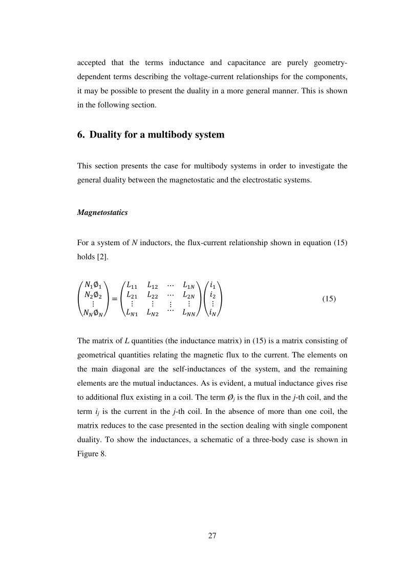
For a system of N inductors, the flux-current relationship shown in equation (15)
holds [2].
(!∅!∅⋮!∅* = (⋮
⋮⋯⋯⋮⋯
⋮*(""⋮"* (15)
The matrix of L quantities (the inductance matrix) in (15) is a matrix consisting of
geometrical quantities relating the magnetic flux to the current. The elements on
the main diagonal are the self-inductances of the system, and the remaining
elements are the mutual inductances. As is evident, a mutual inductance gives rise
to additional flux existing in a coil. The term Øj is the flux in the j-th coil, and the
term ij is the current in the j-th coil. In the absence of more than one coil, the
matrix reduces to the case presented in the section dealing with single component
duality. To show the inductances, a schematic of a three-body case is shown in
Figure 8.

28
Figure 8: Three-Body inductive system
Electrostatics
For a system of N conductors, the electric flux-voltage relationship shown in
equation (16) holds [3].
(,,⋮,* = ¢¢⋮¢
¢¢⋮¢⋯⋯⋮⋯
¢¢⋮¢⋮
(16)
In (16), the charges on each body, Qj, are described in terms of some constant ₵
multiplied by the potential of a body vj. The ₵ constants populate a matrix of
quantities called coefficients of capacitance, and are purely geometric constants.
The potentials are absolute potentials with reference to infinity (a reference which
does not appear on a circuit, as described earlier in the chapter). To show the co-
efficients of capacitance, a schematic of a three-body case is shown in Figure 9,
together with the potentials of each body Vx with reference to infinity (shown as
the earth node in the schematic).

29
Figure 9: Three-body system with co-efficients of capacitance
Discussion of duality
If it is accepted that current is the dual of voltage, then the expression in (15) must
be the dual of that in (16). This means that self-inductance must be the dual of the
self co-efficient of capacitance, and similarly with the mutual terms. If the
analysis is restricted to two body systems, then a two-body capacitor must form
the dual of a two body coupled inductor. This is however not the case at a circuit
level, as shown earlier in the chapter. This is because at a circuit level, a two body
capacitor is regarded as a single circuit component. It was mentioned earlier that
the reason it is considered a single component is that this definition is required to
enable the sole use of voltage differences (as opposed to absolute voltages) in the
circuits domain. This is a mathematical duality then, in that the expressions take
the same form. It is not a circuit level duality and cannot be extended to a circuit
level.
7. Duality for inductive and capacitive coupling
It was shown in preceding section that a general duality between inductance and
capacitance cannot be traced from the governing field equations all the way to a
circuit level. This is mainly due to the fact that at a circuit level, a two-body

30
capacitor is the dual of a single-body inductor. In this section, the two-body
inductive coupling model is presented and an expression is derived for a
capacitive coupling model, for which the duality between the two systems holds at
a circuit level. As before, an analysis of this duality is provided.
Inductance
For this investigation, the analysis is restricted to a two-body system for the
simplest case of inductive coupling. Equation (15) therefore reduces to the well-
known expression shown in (1), after applying Faraday’s law. A circuit diagram
for the system is given in Figure 6.
In (1), L1 and L2 represent the two self-inductances of the inductively coupled
system. The term M is the mutual inductance which arises due to the inductive
coupling. The mutual inductance is equal regardless of which port is used as the
input. The method of determining the values for L1, L2 and M is widely
documented and will not be discussed here.
Capacitance
If a circuit model representing coupled capacitors is to be a dual to the inductive
model shown in (1), the model must have two “self-capacitances” and a coupling
capacitance. It was shown earlier in the chapter that capacitors form two-body
components at a circuit level. This means that the coupling model in the
capacitive case must consist of a four body system, unlike the two body system in
the inductive case. The model should be as shown in Figure 10 with its governing
equation given in (17), where C1 is the input capacitance, C2 the output
capacitance, and S the coupling capacitance of the system. The derivation of this
model is presented in the following section.

31
Figure 10: Capacitive Coupling Model
"" = ' .. '%% (17)
The capacitive model in Figure 10 as well as the inductive model Figure 6 form
two-port networks, and may be referred to as such in later chapters.
7.1 Derivation of Model
Equation (16) describes the electric flux-voltage relationship for a general multi-
conductor system. Since the voltages are absolute, it is not a useful representation
for circuit-level analysis. Through mathematical manipulation, it is possible to
convert Equation (16) to Equation (18), where the C quantities are circuit level
capacitors which are based on the coefficients of capacitance. All primed voltages
are absolute voltages. The terms Cii are the self-capacitances of the system and Cij
(i ≠ j) are the mutual capacitances. Also, a symmetry exists whereby Cij = Cji. The
matrix of C values is often referred to as the capacitance matrix, and the
relationship provides a component-level description of the electrostatic behaviour.
$$⋮, = 01230(12512)3⋯30(12512)30123⋯3⋮'(7′ − 7′) + '(7′ − 7′) + ⋯
0;(1251;2)0;(1251;2)+'7′ (18)

32
Further analysis is restricted to a four body system to fit the form shown in Figure
10. The expression in (18) therefore has the circuit representation shown in Figure
11.
Figure 11: Ten capacitors for a four body system
For the four body system described above, expression (18) can re-written as
shown in (19).
(,,,<,=* =>?
'7′ + '7 + '<7< + '=7='7 + '7′ + '<7< + '=7='<7< + '<7< + '<<7<<′ + '<=7<='=7= + '=7= + '=<7=< + '==7==′@A (19)

33
The expression in (19) is a fourth order expression. This eventually needs to
reduce to a second order mathematical representation in order to form the
expression in (17), with the circuit-level representation in Figure 10.
As was discussed earlier, a circuit capacitor is a two body system, so two bodies
need to be used as the input terminals and two bodies as the output terminals of
the network. Terminals 1-2 are therefore arbitrarily chosen to form the input
terminals with terminals 3-4 to form the output terminals. Clearly it is useful to
express as many voltages as possible in terms of the input and output voltages as
these form the terminals of the device. For the system to remain fully described,
however, it must remain dependent on at least one absolute voltage. Using this
approach, a voltage transformation expression can be developed as shown in (20).
>BBBBBBB?
7′7′7<′7=′77<7=7<7=7<=@CCCCCCCA
=>BBBBB?
1 0 10 0 1 000 1 00 0 0 111 0 01 −1 1 0−11 0 10 −1 1 −1−10 0 10 1 0 −10 @CCCCCA(77<=7′7=′* (20)
It is now possible to rewrite the expression describing the arbitrary four body
system shown in (19), using only the four voltages chosen above. This is shown in
(21).
(,,,<,=* = (' + ' + '< + '=−'−'<−'=
−'<−'<'< + '< + '<< + '<=−'<=' + '= + '<' + '< + '=−'< − '<−'= − '=
−'< − '=−'< − '='< + '< + '<<'= + '= + '==*(77<=7′7=′*
(21)
It is important to recall that absolute voltages are not defined at a circuit level,
therefore some condition needs to be placed such that they are not apparent from a

34
terminal perspective. Recall from the introduction that the aim is to obtain a
duality from a terminal perspective as the network by definition cannot be a
complete dual to mutual inductance.
By inspection of the expression in (21), it is clearly possible to have a different
charge on each of the four bodies. However, it was stated earlier that the proposed
circuit model has one input (circuit-level) capacitor and one output (circuit-level)
capacitor. At a circuit level then, the current which flows through the two input
bodies (the input circuit-level capacitor) must be equal, and similarly at the
output. This is evident from the circuit described in (17). Mathematically this
condition can be applied in terms of charge by the relationships in (22) and (23).
, + , = 0 (22)
,< + ,= = 0 (23)
By expressing the charges in the above expression using their definitions from the
four-body system in (19), the conditions given in (24) and (25) can be obtained.
At this stage the four-body system now comprises of two sets of bodies
possessing the same charge. At a circuit level, this translates to differential
currents at the input and output terminals.
+ '< + '=)7 + (' + '< + '= + ' + '< + '=)7′ + (−'< − '<)7<=+ (−'< − '= − '< − '=)7=′ = 0
(24)
(−'< − '=)7 + (−'< − '= − '< − '=)7′ + ('< + '< + '<<)7<=+ ('<< + '< + '= + '== + '< + '=)7=′ = 0
(25)
The conditions in (24) and (25) provide two equations as functions of four
voltages. It is therefore possible to solve for two voltages in terms of another two.

35
It was mentioned earlier that the absolute voltages may not present themselves
from a terminal perspective, since the absolute reference does not exist at a circuit
level. In order to remove the absolute voltages from the circuit definition, voltages
V2‘ and V4‘ can be solved for in terms of V12 and V34, based on the expressions in
(24) and (25). For the sake of clarity, a short review the procedure used to develop
the model is provided below:
i) A system with four bodies was defined in terms of a mixture of
differential and absolute voltages.
ii) Terminals were chosen for input and output, and all voltages from
above were expressed in terms of input/output voltages and two
absolute voltages, i.e. a total of four voltages.
iii) The condition of differential currents at the input and output was
highlighted, and using this condition it was possible to express the two
remaining absolute voltages in terms of the input/output voltages,
resulting in the system being fully described using only two voltages:
input and output.
Every voltage is now fully described in terms of the input and output voltages: V12
and V34. The expressions are too expansive to print in this chapter, and are
therefore provided in Appendix A. It is clear that Q2 is simply the negative of Q1,
and Q4 the negative of Q3. The terms Q2 and Q4 can therefore be dropped from the
system as they are no longer independent. At this step it is clear that the order of
the system has been reduced from a fourth order system to a second order system.
It immediately follows that the resulting expression fits the form given in (17).
The expressions for the terms C1, C2 and S are given in Appendix A.
Discussion of duality
At this point a capacitive coupling circuit model has been developed which is of
similar form to the inductive coupling model. This model holds as long as the
condition of differential currents at the input and output terminals is externally

36
enforced. In this way the net current flow from the input stage to the output stage
through the self-capacitances is forced to be equal to zero. The absolute voltages
are therefore fully defined, but are not apparent from a terminal perspective. This
had consequences in terms of electrical isolation and is discussed in detail in the
next subsection. From a terminal perspective, the system appears to be a dual to
the inductive coupling model. This duality does not hold at the electromagnetic
level, however, for the simple reason that the one system has two bodies while the
other system has four.
In reducing the fourth order capacitive system to a second order “dual” system,
the input and output capacitances became a complicated conglomeration of the
individual capacitors which make up the system. This is unlike the inductive
model which is physically a second order system where the input and output
inductances are equivalent to the self-inductances of the system. However, similar
to the inductive model, the capacitive model is reciprocal in that the mutual term
is the same no matter which port is used as the input.
Since the developed dual network forms a restricted dual to inductive coupling,
there are certain boundaries in its operation. Deeper insight into the coupling term
and the network as a whole are presented in Chapters 3 and 4.
Electrical Isolation
The capacitive coupling model developed in the above section forms a dual to the
inductive coupling model from a terminal perspective, i.e. the equations
describing the two systems from a terminal perspective take the same form and
differ only in their mathematical symbols. However, it is evident from the
derivation of the capacitive coupling model that the absolute voltages are fully
defined in terms of the differential voltages. The consequence of this is that every
absolute voltage in the circuit, both in the input and output stages, can be solved
for, i.e. there is always a common reference between the input and output, and this
common reference is at a zero potential at infinity. This concept may be better

37
understood by reviewing the circuit diagram in Figure 11, with the zero potential
shown as the earth node.
This means that there cannot be true electrical isolation between the input and the
output of the capacitive coupled circuit model in Figure 10, unlike in the inductive
case in Figure 6. This is despite the fact that it tends to behave as an electrically
isolated system when balanced currents are enforced at the input and output. The
circuit therefore presents one of the cases where despite the fact that an absolute
reference is missing from the model, its existence may have consequences on the
operation of the circuit. This will become evident in Chapter 4.
Simplification of Coupling Model: Level 1
Although the developed capacitive coupling network presents a simple circuit
level description of the electric field coupling, the expressions for each term in the
model are expansive and therefore could complicate its implementation. The
following subsections describe two levels of simplification of the model to ease its
implementation in certain cases.
In most physical four body capacitive systems it may be reasonable to assume that
the bodies will be arranged in proximity to each other such that the capacitors to
infinity (the self-capacitances) will be of similar magnitudes. In such a case, the
model described above can be simplified further by making the self-capacitances
C22, C33 and C44 equal to C11. This gives simplified expressions for the terms C1,
C2 and S. The terms remain too large to print in this chapter and are shown in
Appendix A.
This level of simplification provides slightly less complicated expressions for
each term in the model, and has the benefit of requiring only a single self-
capacitance measurement as compared to the measurement of four self-
capacitances in the full model. It is therefore easier to implement.

38
Simplification of Coupling Model: Level 2
If a physical four body system is set up in such a way that the magnitudes of the
capacitors between the bodies are much larger than the self-capacitances of the
bodies, then it may be possible to neglect the effect of the self-capacitances
altogether. This entails making the values for C11, C22, C33 and C44 equal to zero in
the detailed two port model derived earlier. This leads to a further simplified two
port network description of capacitive coupling, where the expressions for C1, C2
and S are given by (26) to (28).
' = (0F30G)(0G30F)(0F30G30F30G) +' (26)
' = (0F30F)(0G30G)(0F30G30F30G) +'<= (27)
. = (0F0G50G0F)(0F30G30F30G) (28)
It can be noted that the expressions in (26) to (28) correspond to those presented
by other authors referenced in the literature review of this dissertation. In this
dissertation, however, the expressions were developed using a very rigorous
approach with a direct link to field theory. This is as opposed to the papers
discussed in the literature review, where the expressions were developed by
neglecting all the self-capacitors at the outset and then performing a circuit-level
simplification. The fact that different methods were used in literature to obtain the
same result gives confidence in the method presented in this dissertation.
8. Conclusion
A summary of duality was provided to contextualise the contents of the chapter. It
was shown that mutual inductance cannot have a dual in the complete sense, but it

39
is possible in a restricted sense. If a restricted dual is developed, it will have some
operational limitations and these must be fully defined.
Duality between electrostatics and magnetostatics was explored in order to
highlight the link between field level duality and circuit level duality. It was
shown that there are certain inconsistencies in the duality when approached from
different perspectives, and no duality extends from the field level to a circuit
level. This is primarily due to the fact that circuit theory only deals with
differential voltages, whereas any conductor has a self-capacitance with an
absolute voltage; the latter which does not exist on a circuit level. The typical
circuit capacitor is therefore a “mutual capacitor”, i.e. a capacitor between two
physical bodies, unlike an inductor which is inherently a single bodied system.
A capacitive coupling circuit model was developed which forms a restricted dual
to the inductive coupling model. This is physically made up of four conductive
bodies. It is restricted in the sense that it appears to be a dual from a terminal
perspective, but does not form a full structural dual. The absolute voltage of each
body is fully defined internally, but these do not appear on a circuit level as long
as the network is operated with differential currents enforced at the input and
output terminals. Since these voltages are defined, there is no full electrical
isolation between the input and output of the network.
The full capacitive coupling model was simplified to two levels, taking into
account typical possible operating conditions of the model. It was highlighted that
the full simplified model corresponds to those presented in earlier literature,
giving confidence to the method used to develop the model in this dissertation.
9. List of References
[1] Inan A S, Inan U S. Engineering Electromagnetics. Addison Wesley Longman
Inc, California, 1999.

40
[2] Paul CR. Analysis of Multiconductor Transmission Lines. John Wiley & Sons
Inc, New Jersey, 2008.
[3] Elliot R S, Electromagnetics: History, Theory and Applications. IEEE Press,
New York
[4] Skilling H H. Electric Networks. John Wiley and Sons.
[5] Weinberg L. Network Analysis and Synthesis. McGraw-Hill Book Company,
USA, 1962.
[6] Desoer C A, Kuh E S. Basic Circuit Theory. McGraw-Hill Book Company,
USA, 1969.

41
Chapter 3: A deeper analysis of the coupling
capacitance
1. Introduction
In Chapter 2, a term called coupling capacitance was derived and given the
symbol S. This coupling term was shown to be the dual of the mutual inductance
term (usually known as M) to a large extent. This is arguably the most significant
term of the three terms describing the coupled circuit, namely C1, C2 and S,
primarily because it is a quantity that describes the extent of coupling between
two separate circuits. In this chapter, a detailed analysis of the coupling term S is
documented to explore the properties of this term and to compare it with the
mutual inductance term M where appropriate. Experimental verification of
specific scenarios is also provided.
2. Coupling Terms
In Chapter 2, the initial derived expression for the coupling capacitance term S
takes the form shown in (1). Two levels of simplification of this expression were
developed based on typical operating conditions, with the most simplified version
fully independent of self-capacitances. Every version however, takes the form
shown in (1), with f4, f5 and f6 each being a sum of various capacitors, i.e. f4, f5 and
f6 are all positive terms and their definitions can be found in Appendix A. In
order to analyse the coupling term in this chapter, the most complicated form (the
original form) of the coupling term S will be used, so as not to neglect any
information.
= , = (1)

42
3. Analysis
The denominator of the S term is a sum of both self-capacitors and inter-body-
capacitors, and thus cannot have a negative value. It can therefore either assume a
positive non-zero value or a value equal to zero, and this depends on the physical
construction of the four-body system. For the denominator to be zero, the four
body system tends to the case where there is zero coupling between the input and
output stages. Physically this means placing the two bodies comprising the output
terminals far from the two bodies comprising the input terminals. We are
primarily concerned with the coupled case in this dissertation, i.e. where the
bodies are in proximity to each other such that the capacitances are not negligible,
so we will only focus on the situation where the denominator is positive and
greater than zero. In this case, the denominator can be seen purely as a scaling
factor.
The numerator, however, contains a negative sign. Theoretically then, it is
possible to design systems that exhibit one of three types of coupling: positive,
negative and zero. These are discussed below.
3.1 Positive/Negative Coupling
Before designing a system to have either positive or negative coupling, it is
important to know exactly what the sign between the terms in the numerator of (1)
represents in a physical system. In order to do this, it is perhaps useful to consider
the well-known inductive coupled system given by (2).
! = "# $$ # %&'()'*'(+'*, (2)

43
In (2), the M term is the mutual inductance in the system, and shown in Chapter 2
to be a dual to the S term in (1). However, it is not shown in textbooks to have a
mathematical form like S in (1). Despite this, it can also have a positive or
negative polarity and this arises from the physical winding direction of the coils
comprising the system.
The sign of the M term defines the polarity of the induced voltage with reference
to the applied voltage, whilst maintaining positive current flow, i.e. if M is
positive, then the induced voltage will have the same polarity as the applied
voltage, whereas in the negative case the voltages have the opposite polarity. This
is shown in Figure 1 and Figure 2. In the figures the red arrows show the defined
positive current direction, and the red polarity markings show the defined positive
voltage polarity. The blue polarity markings show the polarity of the induced
voltage with reference to the applied voltage, and this corresponds to the sign of
M. The placement of the dots is often used in circuit theory to denote the sign of
M.
Figure 1: Positive mutual inductance

44
Figure 2: Negative mutual inductance
In order to physically achieve a negative value for M, it entails the winding of the
secondary coil in a different direction to that of the primary coil, consequently
changing the direction of flux coupling. However, due to the electrical isolation
between the input and output, if an oppositely polarised voltage is required at the
output, the terminals of the output can simply be interchanged without having any
effect on the coupled circuit. The only case where the sign of the M term matters
therefore is the case of where there is no electrical isolation between the input and
output, for example in the autotransformer. In this case both the load and supply
have a common reference, and the terminals of the output cannot be as easily
swapped around to give an oppositely polarised voltage whilst maintaining the
common reference in the supply and load circuits.
Returning to the capacitive case, the coupled system is given by (3).
" % = "- - %&'.)'*'.+'*
, (3)
As a dual to the inductive case, in (3), the sign of the S term defines the direction
of the induced current with reference to the applied current, whilst maintaining

45
positive voltage polarity i.e. if S is positive, then the induced current will have the
same direction as the applied current, whereas in the negative case the currents
have opposite directions. This is shown in Figure 3 and Figure 4. Similar to
before, the red polarity markings show the defined positive voltage polarity, and
the red arrows show the defined positive current direction. The blue arrows show
the direction of the induced current with reference to the applied current, and this
corresponds to the sign of S. The placement of the dots corresponds to the sign of
S.
Figure 3: Capacitive Coupling Positive
Figure 4: Capacitive Coupling Negative

46
The dot polarity described for the inductive case can therefore be extended to the
capacitive case. Based on the expression for S, it is evident that a negative value
for S can indeed be obtained. The sign of S can therefore be likened to the
winding direction in an inductively coupled system. By modifying the sign of S, a
designer can change the “direction” of the electric flux coupling, consequently
changing the direction of induced current flow, assuming constant voltage
polarity.
It was shown in the inductive case that the winding direction was irrelevant in the
case of full electrical isolation between the input and output, due to the lack of a
common reference point between the two stages. This is different to the capacitive
case, however, as it was shown in Chapter 2 that the reference at infinity forms a
common reference between the input and the output of the network, i.e. the
capacitive coupling network always has a common reference.
Taking the above into account, it is the fact that the system behaves like an
electrically isolated system that is of great importance. This is because even
though current can flow through the self-capacitors to infinity, the differential
current requirement placed at the terminals means that the same current will have
to flow back from infinity into the circuit. This is shown by the red arrows in
Figure 5.

47
Figure 5: Current flow through the self-capacitors
From a terminal perspective, then, the input and output terminals of the network
appear to be electrically isolated from each other. We will refer to this type of
electrical isolation as a pseudo-electrical isolation from this point forward. The
output terminals can therefore easily be switched around to give a different
polarity at the output if required, because at a circuit level, the supply and load
circuits do not have a common reference. The sign of the S term is therefore
irrelevant in the capacitively coupled system just as it is in the inductive system,
despite the fact that the capacitive system is not electrically isolated in the true
sense. In terms of design, the magnitude of the term is the only item of
significance.
It was shown earlier that the sign of the mutual inductance term M becomes
relevant in the case of a common reference between the input and output circuits.
It is shown in Chapter 4 that the physical connection of a common reference

48
between the input and output is not allowed by the capacitively coupled circuit
model as it causes a violation of the balanced currents condition at the terminals
of the network. Since this connection is not allowed, i.e. the model is not defined
in this case; no further conclusion can be made as to the significance of the sign of
S.
Based on the above analysis, it can be concluded that the sign of S holds no real
significance, but instead it is only the magnitude that is of any importance. This
conclusion is valid for as long as the circuit is operated in a region for which the
model is valid, i.e. with balanced currents at the input and output.
The following experiments were done in order to validate the capacitive coupling
model derived in Chapter 2. The first experiment is to test the model’s validity for
an arbitrary setup, followed by experiments with coupling parameters which were
designed to achieve a specific output. These include a system that exhibits 100 %
coupling followed by a system that exhibits zero coupling.
4. Experimental Validation – Arbitrary Coupling
In order to verify the validity of the model for a system with non-zero coupling, a
parallel-plate system consisting of four plates was constructed. A parallel-plate
geometry was chosen because the mathematical expression for capacitance
between parallel plates is very well defined in textbook theory. The setup
comprised of a four-layer PCB with arbitrary plate sizes and 0.1 mm thick FR4 as
the dielectric between the plates. The setup is shown in Figure 6 with a schematic
in Figure 7.

49
Figure 6: The test structure
Figure 7: The test structure schematic
The geometrical properties of the structure are given in Table 1. As shown in the
schematic, length is defined as the horizontal distance and breadth defined as the
length into the page. The quantity d is the vertical distance between plates. The
subscripts are used to show which geometrical dimensions correspond to specific
capacitors, e.g. l12 is the horizontal length of the overlap between plates 1 and 2,
b12 is the distance into the page of overlap between plates 1 and 2, and dxx is the
vertical distance between any two plates.

50
Table 1: Parameters for test structure
Parameter Magnitude
l12 0 cm (no overlap)
l13 3.9 cm
l14 3.9 cm
l23 3.6 cm
l24 6 cm
l34 2.1 cm
b12 0 cm
b13 3.8 cm
b14 4.3 cm
b23 3.8 cm
b24 4.8 cm
b34 3.8 cm
dxx 0.1 mm
ε0 8.854 pF/m
εD ~4
In order to use the full model, the self-capacitances of the individual bodies,
namely C11, C22, C33 and C44 need to be measurable. To achieve this, the parallel-
plate setup was put into a Faraday cage – the body of the cage forming the “earth”
terminal.
Using the physical dimensions in Table 1, it was possible to theoretically
determine the six capacitances definable between the conductors. This was
achieved by using standard parallel plate capacitor theory and the capacitors are
shown in Table 2. The self-capacitance of each of the bodies cannot be easily
predicted using geometrical parameters and thus no prediction was made. All the
capacitor values were then verified experimentally using the measurement routine
in Appendix B and this is shown in Table 2.

51
Table 2: Capacitor sizes for test layout
Capacitor
Name
Capacitance Measured Capacitance Predicted
(nF)
C12 0.003 nF 0.000
C13 1.278 nF 1.262
C14 1.524 nF 1.427
C23 0.264 nF 0.410
C24 2.494 nF 2.390
C34 0.341 nF 0.324
C11 0.000 pF No Prediction
C22 12.00 pF No Prediction
C33 12.00 pF No Prediction
C44 1.225 pF No Prediction
It is clear from Table 2 that there is good agreement between the predicted and
measured capacitances. The differences can be attributed to fringing flux and
inaccuracies in the construction process.
Putting the measured capacitors from Table 2 into the expressions in Appendix A,
the values for C1, C2 and S in the capacitive coupling model were calculated. The
values for C1 and C2 were then measured directly using the routine in Appendix B.
Using two separate load resistors, the value for S was inferred according to the
routine detailed in Appendix B. All calculated and measured values are shown in
Table 3.
Measurements were taken using an Agilent precision LCR-meter for increased
accuracy, with excitation at 1V 1kHz, to minimise inductive effects.

52
Table 3: Circuit Parameters for Arbitrary Coupling
Parameter Measured
Capacitance (nF)
Calculated
Capacitance (nF)
Percentage
Discrepancy - 1.394 1.394 0 % - 1.458 1.459 0.062 % -0.499 (inferred using
50 kΩ load)
-0.499
0 %
-0.499 (inferred using
100 kΩ load)
It is clear from Table 3 that the capacitive coupling model is an extremely
accurate model of the electric field coupling which occurs in a four-body system.
There is almost no discrepancy between the predicted and measured values within
the resolution of the experiment.
This level of accuracy was aided by the controlled environment in which the test
structure was placed, as well as the fact that all electric field effects were taken
into account, i.e. the self-capacitances of the various bodies were not neglected.
An experiment where the structure was not placed in a Faraday Cage and the self-
capacitors were neglected is discussed in a later section.
5. Experimental Validation – 100 % Coupling
In Chapter 4, an expression describing the extent of coupling between the input
and output of a coupled circuit is developed. This expression is given in (4).
= /′1-- ; 0 ≤ /′ ≤ 1 (4)

53
Given this expression, it appears to be theoretically possible to construct a system
such that k’ = 1, i.e. a system which exhibits 100 % coupling. In order to do this,
the process shown in Figure 8 was used, whereby a structure was designed such
that only capacitors C13 and C24 would be significant. In order to do this, a circuit
was set up using two capacitor elements in the layout of the bottom diagram in
Figure 8. The magnitudes of these capacitors are shown in Table 4.
Table 4: Capacitor Values
Capacitor Name Capacitance (nF)
C13 10
C24 10

54
Figure 8: Circuit with 100 % Coupling
For increased accuracy, the circuit was placed in a Faraday cage to allow the self-
capacitors to be easily measured. Following the measurement procedure in
Appendix B, all capacitances were measured and this shown in Table 5.

55
Table 5: Capacitor values for circuit with 100 % Coupling
Capacitor Name Capacitance Measured
C12 2.500 pF
C13 10.02 nF
C14 0.890 pF
C23 0.890 pF
C24 9.991 nF
C34 1.500 pF
C11 3.240 pF
C22 1.500 pF
C33 3.240 pF
C44 1.500 pF
Putting the measured capacitors from Table 5 into the expressions in Appendix A,
the values for C1, C2 and S in the capacitive coupling model were calculated. The
values for C1 and C2 were then measured directly using the routine in Appendix B.
Using two separate load resistors, the value for S was inferred according to the
routine detailed in Appendix B. All calculated and measured values are shown
in Table 6.
Table 6: Circuit Parameters for 100 % Coupling
Parameter Measured Capacitance
(nF)
Calculated
Capacitance (nF)
Percentage
Discrepancy - 5.005 nF 5.007 nF 0.039 % - 5.004 nF 5.006 nF 0.039 % 5.002 nF (inferred using
10 MΩ load)
5.002 nF
0 %
5.002 nF (inferred using
560 kΩ load)

56
In Table 6 we see very good agreement between predicted and measured results.
Using the parameters in Table 6 we can calculate the extent of coupling given by
k’ in the expression in (4). This is shown in (5).
/6 = 71)+ = 8.:: ;<√8.::8;<∗8.::?;< = 0.999 (5)
From (5) it is clear that the designed system exhibits close to 100 % coupling.
6. Zero Coupling
The coupling term S in a capacitive system can be made to have a zero magnitude.
This is a system with bodies arranged such that the voltages and currents sum in
such a way that despite the capacitance between the bodies, there is no apparent
coupling between the input and the output. In order to achieve this, the numerator
of the S term needs to be made equal to zero, i.e. based on (1), the relationship in
(6) must hold.
?- − 8- = 0 (6)
The mathematics does not pose any restriction on a design which allows for (6) to
hold, so the only possible limiting factor is the geometrical structure. A coupled
system was designed to show that it is indeed possible, and this is discussed in the
following section.
6.1 Experimental Validation – Zero Coupling
The aim of this design was a proof of concept rather than optimisation for a
specific application. There are many applications for a zero-coupled capacitive
system, and some are discussed concisely in Chapter 5.

57
Similar to the previous structure with arbitrary coupling, a parallel plate layout
was chosen for simplicity. A schematic for the structure is shown in Figure 9.
Figure 9: Schematic for structure with zero coupling
Using an iterative design procedure, the parameters shown in Table 7 were
obtained to give a system with zero coupling. The subscripts are used to show
which geometrical dimensions correspond to specific capacitors, e.g. l12 is the
horizontal length of the overlap between plates 1 and 2, bxx is the distance into the
page of overlap between any two plates, and dxx is the vertical distance between
any two plates.

58
Table 7: Parameters for system with zero coupling
Parameter Magnitude
l12 1 cm
l13 2 cm
l14 15 cm
l23 2 cm
l24 3 cm
l34 0 cm (no overlap)
bxx 10 cm
dxx 0.01 mm
ε0 8.854 pF/m
εD ~4
In this experiment, the test structure was not placed in a Faraday cage, and thus
the self-capacitances of the bodies could not be easily measured. It is shown later
that in this particular case, the neglect of the self-capacitors does not have a major
effect on the results.
Using the routine in Appendix B which neglects self-capacitances, the magnitudes
of the six inter-body capacitors were measured and these are shown in Table 8.
Table 8: Capacitor sizes for zero-coupled layout
Capacitor Name Measured Capacitance (nF)
C12 0.094
C13 0.457
C14 0.933
C23 0.403
C24 0.741
C34 0.006

59
Based on the measured capacitances, the expression in (6) is very close to zero as
shown in (7).
?- − 8- = 37.36 × 10 F (7)
Using the measured capacitors, the values for C1, C2 and S were determined, and
these are shown in Table 9. These parameters were also experimentally
determined using the routine described in Appendix B. The experimental values
are also provided in Table 9.
Table 9: Circuit Parameters for zero-coupled layout
Parameter Measured Capacitance (nF) Calculated
Capacitance
Percentage
Discrepancy - 0.720 nF 0.721 nF 0.139 % - 0.571 nF 0.574 nF 0.525 % 15.62 pF (inferred using 220 kΩ
load)
14.52 pF
7 %
It is clear from Table 9 that there is very good agreement between the values
predicted using the model and the values which were measured directly. Although
there is a 7 % discrepancy in the S parameter, this is considered acceptable as the
order of magnitude of S is much smaller than that of the parameters C1 and C2.
This slightly higher error level can be attributed to the difficulty of the inferred
measurement – since S is so small (designed to be zero), the input impedance
barely changes when a load is applied to the output. At this resolution, parasitic
effects such as temperature drift become apparent and may have affected the
measurement slightly.
Since the capacitive coupling model used in this experiment was the simplified
model which neglects self-capacitors, the high level of agreement between
predicted and measured results show that in this case the neglect of self-capacitors

60
is a valid assumption. Evidently the relative magnitudes of the self-capacitors are
much smaller than the inter-body capacitors, and this is achieved by the
construction of the structure where the bodies had large overlap area and small
inter-body distance.
Using expression (4) to quantify the coupling of this system, we get (8).
/6 = 71)+ = 8.F G<√:.H :;<∗:.8H;< = 0.024 (8)
Based on the results above, it is clear that it is indeed possible to construct a
system which exhibits close to zero coupling as predicted by the model.
7. Conclusion
An in-depth analysis was done into the properties of the coupling capacitance S
which forms part of the capacitive coupling network developed in Chapter 2. It
was shown that although a designer can obtain positive, negative and zero
coupling with a four-body system, there is no real significance in the sign of S as
the output terminals can easily be switched to obtain a different voltage polarity. It
was also shown that this holds regardless of the fact that the system is not fully
electrically isolated, since it behaves like an electrically isolated system when the
condition of balanced currents is enforced at the input and output terminals.
Experimental verification of three capacitively coupled systems were documented.
These included a case with arbitrary coupling between the input and output, a case
with close to 100 % coupling and a case with close to zero coupling. All
experimental evidence showed excellent agreement with the results predicted by
the capacitive coupling circuit model. This shows that the model can indeed be
used to describe the electrostatic behaviour of an arbitrary four body system.

61
Chapter 4: Properties of the Capacitive
Coupling Model
1. Introduction
In the previous chapters, the need was highlighted for general circuit theory to
support capacitive coupling in a similar way that inductive coupling is described.
A circuit model for a four body system was then developed from the field level
theory which formed a dual to the inductive coupling model. A term called
“coupling capacitance” was defined to be the dual quantity to mutual inductance,
and this quantity was explored in detail in Chapter 3. Experimental verification
showed good agreement between the theory and a physical system.
At this point, a “new” circuit component has been developed. In this chapter,
certain circuit properties of this component are explored in order to gain insight
into the operation and limitations of the component. For reference purposes, the
capacitive coupling model is shown in Figure 1 with the governing equation in
(1). The inductive coupling model is shown in Figure 2 with its governing
equation in (2).
Figure 1: Capacitive Coupling Model

62
= (1)
Figure 2: Inductive Coupling Model
= (2)
2. Circuit Properties
Typical circuit properties are discussed in the following subsections.
2.1 Linearity, Memory and Causality
The system of equations which describe the capacitive coupling model is easily
shown to be linear under the condition that the coefficients C1, C2 and S are linear.
Since these quantities translate to physical capacitors, the condition imposed for

63
the system to be linear is that the dielectrics of the capacitors be linear. In the
inductive model, the requirement for linearity is that the permeability of the
magnetic core is linear. The linearity property thus appears to impose similar
requirements in both the capacitive and inductive coupling models.
Since the voltage-current relationships of a capacitor are based on values at
previous time intervals, the capacitive coupling model can be said to have
memory. There is no future dependence, so the system is causal. These properties
also hold in the inductive coupling model.
2.2 Energy Storage
In order to develop the capacitive coupling circuit model, the only condition
which was placed on the general four-body coupled system is that there are
differential currents at the input and output ports. This condition implies that there
is zero net current flow from the input side of the network to the output side. By
enforcing this condition, the system is fully described by the parameters as
described in Appendix A. The energy storage of the system can therefore be
calculated as follows.
Short circuit the output port V2. Let V1 increase from 0 V up until V1’. The total
energy stored in the network is given by (3), where P represents power.
= = = = ′ (3)
Let V1 remain constant, i.e. = 0. Now let V2 increase from 0 V up until V2’.
The total energy stored in the network is given by (4).

64
= " = + "
+ " ′
= 12 ′ + 12 ′ + ′
(4)
Since the system is linear, the expression for total energy stored is the same if the
procedure is reversed. The expression in (4) is the dual to the expression in (5)
which represents the energy storage in a two-body inductively coupled system.
& = + + (5)
In order to verify the expression in (4), an arbitrary four body system was
simulated using the circuit model and the total energy was calculated using (4). A
similar four body system was then set up in a FEM package and the field energy
was computed numerically. The energy calculated using these two methods were
found to be identical.
2.3 Limit on Coupling Capacitance
In the inductive model in (2), the inductances on the off diagonal of its co-
efficient matrix Lii correspond to the self-inductances of the system, and the term
M on the main diagonal is the mutual inductance of the system. Both quantities
have a direct link to the field level theory.
If it is stated that the capacitive model in (1) is the circuit level dual to the
inductive model in (2), then at a circuit level the self-inductances must be the
duals of the Cii terms on the off diagonal of the capacitive co-efficient matrix in
(1). The same relationship applies to the mutual terms on the main diagonal. It is
important to recall, however, that these relationships do not extend to the field
level.

65
In an inductively coupled circuit, the mutual inductance can be expressed in terms
of the self-inductances of the system, as shown in (6). The term k is a ratio defined
to indicate the “extent” of the coupling between the two coils.
= (); 0 ≤ ( ≤ 1 (6)
The question arises as to whether or not a similar expression to (6) can be found
for the capacitively coupled system. In order to do this, boundary conditions must
be applied to the system to determine the maximum value for the mutual term S.
Recall the expression for energy storage in (4). To find the maximum value for S,
a boundary condition that can be enforced is that the energy storage in the
capacitive coupling system must be minimised. This condition is physically
realised when the coupling term S is negative, giving an expression for energy
storage is given (7).
= + − (7)
Since the energy storage of the system is always greater than or equal to zero, this
reduces to the expression in (8).
+ ≥ (8)
By completing the square and solving for S, the expression in (9) can be derived.
≤ ) ./0123334 = (′); 0 ≤ (′ ≤ 1 (9)
Based on the analysis above, it is shown that in a capacitively coupled system, the
coupling capacitance S can be expressed in terms of the two capacitances C1 and
C2, similar to the inductive coupling case. A coupling term k’ can also be defined

66
to describe the “extent” of the coupling in the network. This property ties in with
the dual nature between the inductive and capacitive coupling networks.
3. Applications of model
This section describes some important applications of the capacitive coupling
model with comparisons to the inductive coupling model.
3.1 Theoretical Application: Interconnections between networks
One of the main benefits of two-port modelling is the ability to analyse
complicated networks in terms of combinations of different two-port network
circuits. The converse of this is to construct a complicated network using two-port
network components in various combinations. Two-port networks can be
interconnected in a few basic ways, namely: series, parallel and cascade. These
can be split into two groups and are discussed separately below.
Group 1: Series and Parallel Connections
For a two port network interconnection in this group, the two port parameters
describing the interconnected network is simply the sum of the component
network parameters, as long as a set of validity tests known as the Brune tests
hold [1]. The Brune tests verify that each component network behaves the same
way when it is interconnected as it does in isolation, by verifying that the input
and output ports have differential currents even when interconnected. These
interconnections are shown in Figure 3 and Figure 4.

67
Figure 3: Two Port Series Connection
Figure 4: Two Port Parallel Connection
Recall from Chapter 2 that in the inductive coupling model, the two-port network
representation has a direct link to the physics upon which it is based. Since the
model and the physics show no electrical connection from the input to the output
stages of the network, the condition for differential currents at both ports is
internally enforced by the physical system. Because of this, the Brune tests are
inherently satisfied, allowing any combination of the above interconnections to be
made. The two-port representation of the interconnected network is therefore the
sum of the component two-port parameters.
In contrast, the capacitive coupling two port model requires that the condition for
differential currents should be externally enforced for the model to hold. This
means that the Brune tests do not necessarily hold in any arbitrary

68
interconnection, and thus the two-port parameters describing the interconnected
network is not necessarily the sum of the component network parameters. Further
analysis needs to be done on an interconnected system to develop an input-output
model. Alternatively, a 1:1 transformer can be used between each interconnection
to ensure differential currents at the ports and satisfy the Brune tests; after which
the two-port representation of the interconnected network will be the sum of the
component two-port parameters.
Although a difference in the operation of the inductive and capactive models is
highlighted here, it does not show a breakdown in the duality theory at a circuit
level. A condition for the duality was that differential currents must be enforced,
and as long as this condition is satisfied the models can be interconnected in the
same way.
Group 2: Cascade interconnection
This type of connection can be made between arbitrary component networks, and
the two port parameters of the interconnected network is simply the product of the
parameters of the component networks. It is shown in Figure 5.
Figure 5: Two Port Cascade Connection
The cascade connection can be made for both the inductive and capacitive
coupling two-port networks, and the condition for differential currents is
inherently satisfied due to the terminations of the interconnected network on both
ends.

69
3.2 Theoretical Application: Arbitrary configurations
Due to the physics upon which the inductively coupled circuit is based, the output
stage may be connected to the input stage of the circuit in either a series or
parallel configuration whilst maintaining the coupling; however the electrical
isolation will be lost. A common case of this is in the autotransformer, where a
series connection is made between the input and output stages, as shown in Figure
6.
Figure 6: Autotransformer configuration
The inductance looking into the input terminals is given by (10).
567 = + ± 2 (10)
Based on the duality between the two port representation of capacitive coupling
and inductive coupling, a similar expression can be found for the capacitance

70
looking into the input terminals when a series connection is made. However, this
expression does not carry through to a field level.
The reason for the breakdown in the duality in this particular application is that
the condition upon which the capacitive coupling model is based is not satisfied.
This condition is that the input of the circuit must be applied between two bodies,
and the output between the other two bodies; and there must be differential
current at both the output and the input ports. However, in the case of the
autotransformer, the output is tapped off between one of the original output ports
and one of the input ports, i.e. a common reference is used for both the output and
input. The two-port capacitive coupling model therefore cannot be used in any
configuration that entails the use of a common terminal for both the input and
output. A different model needs to be developed based on the physics of the
system to allow for the two cases of 1) a single common terminal between the
input and output (the series connection); and 2) two common terminals between
the input and output (the parallel connection).
Although it was stated above that the model fails when a common reference is
implemented between the input and output, a significant difference of the
capacitive coupling model can be highlighted. In an inductively coupled circuit,
there is only a single configuration that can be used such that there will be
electrical isolation between the input and output circuit, and this is the
configuration as shown in (2). However, in the capacitive coupling model, it is
simply a condition that the input be applied between two bodies, and the output
between two bodies. This means that as long as this condition is satisfied, any
configuration of input/output ports will achieve pseudo-electrical isolation, as
shown in Figure 7. Pseudo-electrical isolation is discussed in detail in Chapter 3.
All of the combinations of input/output ports for a four-body system are shown in
Table 1. To aid with this concept, the similarity between the networks in row 1
and row 2 of Table 1, using the same four bodies is shown in Figure 7.

71
Table 1: Configurations of capacitive coupling system
Input port terminals Output port terminals
1-2 3-4
1-3 2-4
1-4 2-3
Figure 7: Capacitive Coupling showing alternate excitation

72
In order to use the various configurations shown in Table 1 in a circuit, it is
simply a matter of substituting for the individual capacitors in the same two-port
model described in this dissertation. This difference arises from the physical basis
of the capacitive circuit, due to the fact that the capacitive coupling circuit is a
four-body system as compared to the inductive circuit which physically consists
of two bodies.
4. Use of the circuit model in circuit analysis
With the properties of the capacitive coupling circuit model described in the
preceding sections, it is perhaps useful to show how the model can be used in
circuit analysis. In this regard, a few examples are provided in Appendix C.
5. Conclusion
In this chapter, certain circuit level properties of the capacitive coupling model
were explored to gain insight into the operation and limitations of the model. It
was shown that the properties of linearity, memory and causality hold in a similar
way that it does for inductive coupling. An expression for total energy storage in a
capacitively coupled network was developed, and this expression also appears to
exhibit a duality with the expression for energy storage in an inductively coupled
network. Using the expression for energy storage, an expression for the maximum
value of the coupling capacitance of the network was developed. This is also
shown to be of similar form to the inductively coupled network.
Interconnections between multiple capacitively coupled networks were then
explored, and it was found that in general these connections can be made without
the duality breaking down, as long as the condition of differential currents at the
input and output of the network is enforced. It was then mentioned that it is not
possible to enforce this condition when there is a connection of a common

73
reference between the input and output of the network - hence this type of
connected is not allowed by the model.
A difference of the capacitive coupling model was then highlighted in that the
model can be used to describe a system with any set of ports chosen as the input
and the other set as the output. This is not the case with an inductively coupled
system.
Lastly, general examples are provided detailing how to use the model in standard
circuit analysis.
6. List of References
[1] Ruston H, Bordogna J. Electric Networks: Functions, Filters and Analysis.
McGraw-Hill Inc, USA, 1966.

74
Chapter 5: A Discussion on Typical
Applications for the Capacitive Coupling
Circuit Model
1. Introduction
In the previous chapters, a circuit model was developed to deal with capacitive
coupling between four conductive bodies. In this model, the input is applied
across two bodies and the output is tapped off the other two bodies. The aim of
the model was to further develop general circuit theory, as there was no
consistent, rigorously defined capacitive coupling circuit model similar to the
well-known inductive coupling model. This meant that many designers used
different circuit models in different applications and it was difficult to make any
comparisons between different systems. Since the model derived is general in
nature, it has the potential to be used in a variety of applications and allow
comparisons to be made between different systems.
In this chapter, typical practical applications of the capacitive coupling model are
documented. For each type of application, a discussion is provided as to whether
or not the use of the capacitive coupling model would be advantageous. The list of
applications provided is by no means an exhaustive list of all possible
applications, but rather a concise group of different applications to give the reader
an indication of the possible widespread benefits of such a model.
2. Applications
Typical applications are discussed in the following subsections.

75
2.1 Tapping power from overhead transmission lines
The presence of AC voltage on floating conductors in proximity to high voltage
overhead AC transmission lines has received much attention in literature. This
voltage can exist due to three mechanisms: conductive coupling, inductive
coupling and capacitive coupling [1]. The voltage due to the coupling is often
undesirable as it can result in electric shock when humans or animals come into
contact with it. In these cases, it is important to take the electric fields into
account, and implement measures to mitigate its effect. In order to do this, some
sort of modelling of the coupling effect must be done. With this in mind, Al-Badi
and Salam [1] developed a finite-element-modelling based system to predict the
voltage on a gas pipeline in the vicinity of an overhead transmission due to
capacitive coupling. Although this model gave good agreement to an experimental
setup, it is limited in that it is not a circuit model, and as such cannot easily be
used to describe the interaction between the capacitive system and other circuit
systems which may be present.
While the case described in the preceding paragraph had undesirable coupling,
there are also applications where capacitive coupling can be used for beneficial
purposes. One such application is the Sishen-Saldana railway link in South Africa,
where the locomotive is powered by the high voltage overhead line [2]. In this
application, there is no low-voltage supply easily available alongside the train for
track-side services, and other options such as step down inductive transformers
and PV arrays are not feasible or viable solutions. In his paper [2], Nicolae
presents a capacitive coupling model that allows for sufficient energy tapping off
the transmission line for powering up of these devices. This model is an analytic
model, and corresponds to the simplified model (neglecting self-capacitance)
presented in Chapter 2 of this dissertation. It is shown experimentally that the
model does in fact give good agreement with experimental data, and can be used
in such a situation.

76
Another use for capacitive power tapping off transmission lines is for powering
cellular masts in remote locations. In recent years, mobile phone usage has
become very widespread, to the extent that there are more mobile phones in use
than traditional landline phones. Because of this, cellular network operators are
continuously increasing their network coverage to support the increasing number
of subscribers. In urban areas, this is not too difficult as there is generally a power
source easily available. However, this is not necessarily the case in outlying areas
where there is no electrical infrastructure available. Blais and
Berthiaume [3] proposed a method of tapping power from the overhead ground
cable of an electric power transmission line. The mechanism upon which it is
based is capacitive coupling. This is widely regarded as the more economical
method of capacitive power tapping as compared to the use of a capacitive voltage
divider [3].The basis of their work is that capacitive coupling gives rise to a
voltage on the overhead ground cable due to the group of electrified 3-phase
cables in its vicinity. This voltage can be used as a voltage source to power a
device. This setup is shown in Figure 1. Using this information, they derived a
Thevenin circuit model of the setup; the output of which provides the power to the
cellular mast as shown in Figure 1. In a test case of a 735 kV transmission line,
they were able to tap off 2 kW of power for every kilometre of wire length.

77
Figure 1: Power tap off from ground wire
In terms of their design process, although they proposed that the mechanism of
power transfer was capacitive coupling, the capacitive effects were not modelled,
and assumed to be uniform for the length of the line. There is no measurement of
these capacitances with a link back to the proposed circuit model. Instead, the
voltage between the overhead ground and earth was simply used as the two
terminals providing power to the cellular mast. Because of this, the only method
to optimising power transfer is to increase the length of the line.
In the case where the capacitances are uniform and no modification is made to the
overhead lines, this simplified approach is fully valid and gives good experimental
results as shown by the authors. However, it is extremely limited in that the output
cannot be predicted theoretically as the capacitances are unknown.

78
In order to have a more general approach to capacitive tap-off from overhead
transmission lines, it will be useful to use a capacitive coupling circuit model such
as the one derived in Chapter 2. In order to use the model, it is required that there
are differential currents at the input and the output terminals, as shown in Figure
2. Similar to the paper discussed above, the overhead ground cable and earth can
be used as the two output terminals since the condition of differential currents at
the output will be enforced by the powering a passive load.
At the input, the three 3-phase cables can again be modelled as a single body, and
this forms one of the input terminals. This is possible since the three 3-phase
cables are at different potentials, and their electric fields add to give a resultant
field in space. Due to phasing, this resultant field will only be non-zero within
close proximity to the group of cables, and further investigation is required to
quantify this exact distance. It is not possible to use earth as the second input
terminal because a common reference between the input and output is not allowed
as discussed in Chapter 4. To get around this, a test conductor can be inserted into
the field to form the second terminal at the input. In this way, the condition of
differential currents at the input can be enforced. The test conductor can have any
geometry and placement, such that the system gives the desired output. This gives
the designer the benefit of a level of variability in the design, i.e. the designer is
not entirely restricted by the geometry of the lines.
Investigation must be done into the consequences on the surrounding fields due
to the placement of a test conductor, as well as the maximum distance from the
group of three-phase lines at which the resultant electric field will be of a
magnitude such that it can be modelled as a single body.

79
Figure 2: Power tap off from ground wire using model

80
The advantage of using this type of system is that the fourth body (the test
conductor) can be designed and placed specifically to optimise power output,
since the other three bodies have no variability. Also, the output can be
determined theoretically for any given geometry of transmission lines at any
voltage. Therefore this is not only a more comprehensive model than the
traditional one, but it also offers designers more flexibility in a design of such a
system.
2.2 Human Proximity Sensors
There are many applications where some sort of human proximity sensing is
required. Generally these sensors are used to preserve the safety of human beings
who are in proximity to some sort of machinery. One of these applications is
presented in [5], where the authors describe a proximity sensor which detects a
human close to the blade of a chainsaw, and implements electricity cut-off. The
mechanism of operation is simple as shown in Figure 3 – a transmitter plate is
placed on the one side of the blade and a receiver is placed on the other. A
switching waveform is applied to the transmitter plate and the voltage at the
receiver plate is measured. Capacitors are defined between the various bodies as
shown in Figure 4. Because of the grounded blade placed between the transmitter
and receiver, there is a weak capacitance between the two plates and it relies on
fringing flux. When a human body part enters that field, it disturbs the flux and
less voltage appears at the receiver. It is found that by using this mechanism, a
human hand can be detected at a distance of 15 cm, and false alarms are not
triggered by the presence of wood.

81
Figure 3: Proximity Sensor for Chainsaw
Figure 4: Chain saw proximity sensor circuit

82
It is clear from Figure 4 that the circuit is made up of four bodies can be
simplified using the model presented in this dissertation. An alternative circuit
model for this application is shown in Figure 5. By using the setup in Figure 5, it
is not a requirement that the blade be connected to physical ground, unlike the
circuit used in [5]. The ground symbols used in Figure 5 therefore refer to the
absolute zero reference, or infinity, to which all bodies have a self-capacitance.

83
Figure 5: Using Capacitive Coupling Model for Chainsaw

84
Other applications of human proximity sensing can be found in buildings where
existing electrical infrastructure is utilised to detect human presence and
implement measures such as powering on lights or activating an alarm. In a higher
voltage environment such as an electrical substation, human proximity sensors
can be used to raise an alarm if a person steps too close to a live installation.
Buller and Wilson [6] described a method of measurement and modelling the
coupling capacitance between electrical wiring in buildings and humans. The
technique employed to measure the coupling capacitance between the human and
the electrical wiring was to make use of a musical instrument called a theremin.
This device operates on the principle that the human acts as a conductor with a
capacitance to ground, and modifies the capacitance controlling the frequency of a
variable frequency oscillator. The signal is compared to a fixed frequency
oscillator, and the change in capacitance observed due to a human interacting with
the field can be found as a function of the difference between these two signals. A
series of experiments were performed with different humans and a numerical
consistency was found in the results obtained for specific distances away from the
electrical wiring. It was found that this type of sensor could predictably detect the
proximity of a human up to a distance of 1 m away.
An analytic first order model was then proposed to represent the coupling effect,
and the model results agree with the measurements taken using the theremin only
in terms of order of magnitude.
Although the analytical model presented by the authors of the paper does have a
level of agreement with experimental results, it is a very crude estimation of the
capacitive effects which are manifest in such a setup. The model is not detailed
enough to use as a basis for a design of such a system, but merely provides a step
in the right direction. The authors mainly focused on the experimental setup to
measure the capacitances and show that there is indeed a capacitive coupling that

85
occurs between humans and wiring, and that this coupling is large enough to be
measureable.
In order to fully represent the electric field effects that are manifest, a much more
comprehensive analytical model is required. The capacitive coupling model
presented in this paper takes into account all electric field effects in a four body
system, and this can be beneficial in such an application. A proposed setup is
shown in Figure 6.

86
Figure 6: Human Proximity to Wall Wiring

87
In this particular application, there is electric wiring in the walls of the building. It
is reasonable to assume that there is an outgoing and return cable in the walls for
the electric supply, and these form two bodies. Outside the wall is the person. It is
proposed that the person wears a conductive body on their person, which is not
electrically connected to their body, e.g. an armband. In order to enforce the
condition of differential currents at the output port, a load can be used with a
connection to the band and the human. Depending on the coupling, a certain
amount of power can be dissipated in the load, and this gives an indication of the
proximity of the human to the electric cable. This kind of setup can also be used
in high voltage installations, where a light can be made to glow on a person’s
armband to notify him when he moves his hand close to an electrified line.
The advantages of using the proposed model instead of the one detailed in the
paper include the fact that all capacitive effects are fully modelled. The model
also allows for calculation of outputs for any arbitrary configuration of wiring and
human proximity.
2.3 The Electric Transformer
3-D integrated circuits have emerged in recent years as one of the technologies
necessary for use in high end processing chips. The benefit of the extra dimension
is that it allows for parallel processing power with short interconnects [7]. One of
the main challenges in manufacturing 3-D chips is that of transferring data and
power across the various layers, as galvanic connections restrict the layout and
design of the chip significantly. While there have been methods proposed for data
transfer between layers such as optical and inductive vias, these do not compete
with the interconnect density of galvanic connections; and the power transfer
across different dies is still an issue [7].

88
Culurciello and Andreou proposed a method of using capacitive coupling between
different dies on a 3-D chip to allow communication as well as power transfer
between different layers [7]. This is shown in Figure 7.
Figure 7: Capacitive Power Transfer for 3-D chips
The concept behind their approach is to have metal pads on different layers. These
pads are aligned accurately to overlap each other, and these form parallel-plate
capacitors across which displacement current can flow. In this way, power and
data can be transmitted across layers, with each power transfer circuit requiring a
minimum of two capacitors to complete the circuit. Using this concept, a power
supply circuit was developed and an expression was developed to show the
relationship between output current and the physical geometry of the capacitors.
The setup was tested experimentally and found to yield good results. For their
application, a reasonable amount of power was transferred using capacitive
coupling, and it is shown that capacitive power transfer is a very viable
technology for use in 3-D circuits.

89
Although the authors attempted to transmit power across layers using capacitors, a
very fundamental assumption was made in their approach, namely that each two-
body capacitor does not interact with the bodies alongside them. In other words it
is assumed that the capacitors are very well defined in terms of their construction,
and there is no coupling between the two capacitors which make up the power
transfer circuit. There is a lot of precision in the design of 3-D integrated circuits,
so this assumption is a reasonable assumption to make. However, in the case
where the capacitors are brought very close to each other due to space constraints,
this may pose a problem. For a more general approach then, it is beneficial to
make use of the capacitive coupling model derived in Chapter 2. This takes all the
effects of capacitive coupling between four bodies into consideration, and will
provide a much more accurate model for the circuit.
A second application of capacitive power transfer is that of battery charging. Due
to technological developments in recent years, most consumer devices have some
sort of battery built in to the device to allow for mobility. Some of these include
mobile phones, mobile computers, electric toothbrushes and electric cars. One of
the biggest inconveniences of these devices is that they need to be plugged in to
an electrical supply to get charged, and this often entails making a direct contact
between the supply and the device using a cable. There have been many methods
proposed to wirelessly charge devices in the past as it offers many benefits,
including convenience and electrical isolation [8]. The most common technique
used for wireless power transfer is inductive coupling, however this has its
limitations. Another method to achieve wireless power transfer is to use capacitive
coupling, and this has been used in niche applications. A typical example was
investigated by Hu, Liu and Li in [9], where the authors developed a contactless
battery charging system for a soccer-playing robot.
In this application, the authors developed a stationary power supply circuit with
two flat plates, and a mobile power receiving circuit with another two flat plates,
similar to the circuit shown in Figure 7. The method of operation is that when the
battery charge on the robot falls to a certain level, it would return to the charge

90
station, and the plates would line up. When these plates are aligned, there is a
well-defined capacitance between the plates on the stationary and mobile circuits,
and due to the high frequency of operation, displacement current flows across the
plates, completing the circuit.
This device is seen to give good experimental results, however, it is exceptionally
limited in its design. Firstly, the authors rely on good coupling of plates between
the stationary and mobile units, and zero coupling between the two plates on the
stationary unit or the two plates on the mobile unit. The immediate consequence
of this is that when the mobile unit is not charging, there will still be coupling in
the stationary circuit, resulting in unnecessary power draw. Also, the mobile unit
must align itself perfectly with the stationary unit when charging. If this does not
happen, the coupling is not predictable. Another consequence is that the
capacitances of their circuit must be very well defined if the other coupling
capacitors are to be ignored (the capacitor between the stationary plate 1 and the
mobile plate 2 and vice versa). Also, the self-capacitance of each plate is ignored
entirely.
The factors mentioned in the previous paragraphs can potentially lead to many
limitations in the general applicability of the approach used by the authors. If the
capacitive coupling model discussed in this dissertation is used instead, many of
these limitations can be accounted for and a much more general device can be
designed. It is notable that this type of charging is not restricted to the niche
application of soccer-playing robots, but rather it can be extended to wireless
mobile phone chargers and the like.
2.4 Minimisation of parasitic capacitance in inductor windings
In the design of high frequency inductors, there is much emphasis placed on the
electromagnetic coupling, where unwanted capacitive coupling takes place
between windings in the inductor. This is especially true for filter inductors like

91
the one shown in Figure 8, where the capacitance between the windings leads to
displacement current flow across the windings rather than conduction current
through them. This effect is exacerbated by the high frequency of operation. There
have been a number of measures proposed to reduce this effect by varying the
placement and orientation of components, or by modelling it using finite element
analysis [10], however these measures are non-general in nature. As such, it is
difficult to use this theory in any arbitrary configuration.
Hofsajer [11] and Wang [13] proposed a capacitive coupling circuit model to deal
with the inter-winding capacitance for minimisation of the parasitic effect in a
high frequency inductor.
Figure 8: High Frequency Inductor
This capacitive coupling model presented in [11] and [13] to represent the
parasitic effect is identical to the simplified model derived in Chapter 2, where the
self-capacitances were ignored. This is shown in Figure 9.

92
Figure 9: Capacitive Coupling Model
Using this model, an experiment was set up to arrange conductors in a layout to
minimise the coupling term. A planar inductor, which usually gives problems at
higher frequencies due to inter-winding capacitance, was built with the sizing of
the plates accurately determined for coupling minimisation.
This was compared to a similar planar inductor which was not optimised for
coupling minimisation. The results obtained show that the model indeed
represents the coupling behaviour in such a configuration, and can be used to
design inductors such that the coupling can be minimised.
Although the analysis performed by Hofsajer [11] was done on a planar inductor,
the approach can easily be extended to the more common wound inductor. This
means that the model can be used to reduce parasitic capacitance between
transformer windings as well, by making use of a negative or zero coupling term
as discussed in Chapter 3.

93
2.5 Capacitive Crosstalk
Ribbon cables are commonly used in electronics because they offer numerous
benefits over other types of cable in certain applications. A typical commercially
available application is that of medical ultrasound probes [12]. In this application
it offers the benefits of improved ergonomics, decreased capacitance and lower
cost than the conventional co-axial cable [12].
The typical configuration of four-wire ribbon cable and its electrical model are
shown in Figure 10 [12]. This configuration represents a section of the ribbon
cable, i.e. the terminations of the individual cables are not included in the model.
The purpose of the multiple ground wires is to electrically shield each of the
signal wires from each other, i.e. instead of signal wires coupling with other signal
wires, they now couple with adjacent ground wires, thereby reducing the coupling
between different circuits. Although the coupling between signal wires is now
reduced, it cannot be assumed to be zero. However, it is clear from Figure 10 that
the typical circuit model for the cable neglects the coupling which still occurs
between the signal wires, i.e. it only takes into account the coupling between
adjacent wires.
Figure 10: Ribbon Cable

94
The authors of [12] have highlighted that despite the enhanced crosstalk-reducing
properties of ribbon cable, the crosstalk remains a problem in the design of the
probes. This crosstalk arises due to imperfect shielding of the signal cables by the
ground cables over a certain length.
To reduce the effect, the authors proposed that instead of the constant spacial
separation used in conventional ribbon cable, a variable geometry ribbon cable
should be used. Since the cable has a variable geometry over its length, the
lumped model in Figure 10 can no longer be used. As an alternative, they
proposed a model using Multiconductor Transmission Line (MTL) theory to
compute the per unit capacitances along the line. These distributed quantities were
lumped for certain sections, and these sections were cascaded to form the full
model for the cable.
Using this model together with a variable geometry cable, it was found in
simulation that the capacitive coupling could be reduced as compared to a
standard ribbon cable.
It is evident from the above discussion that in the simplified case of Figure 10, the
capacitive coupling between signal wires is not modelled at all. To solve this
problem the authors of the paper developed a second model which is much more
complicated than the one in Figure 10. As an alternative to the model presented in
the paper, the capacitive coupling model in this dissertation can also be used, as
shown in Figure 11.

95
Figure 11: Ribbon Cable using Capacitive Coupling Model

96
Based on the modelling in Figure 11 it may appear that a common reference is
created between the input and output in the capacitive coupling model, due to the
ground cables being short circuited at the cable terminations. Recall from
Chapter 4 that the capacitive coupling circuit model is not valid when the
connection of a common reference is made. This issue is addressed by the
discussion in the following paragraphs.
For the circuit in Figure 11, the return current of cable 1 flows only along cable 2,
and the return current of cable 3 flows only along cable 4 since these are the paths
of least inductance. However, at the termination of the cable, cables 2 and 4 are
connected to each other as they both form the same digital ground.
However, due to the high frequency switching signals in the cable, inductive
effects along its length are no longer insignificant, and this gives rise to voltage
drops along the length of cable. Thus, despite the fact that cables 2 and 4 may be
connected to each other at the termination of the cable, the inductive voltage drops
along the length of the individual lines result in the two cables being at different
potentials along their lengths. This means that if a small section of cable is
considered, cables 2 and 4 will be at different potentials and will not appear to be
connected to each other. As a result, the capacitive coupling model can be used to
model the electric field coupling manifest in a ribbon cable used for high
frequency switching signals.
Figure 11 therefore shows a simple alternate circuit model to the one presented in
the paper, and takes into account the capacitive coupling between signal wires in a
ribbon cable. In the case where a variable geometry ribbon cable is used to reduce
the coupling effect, this model can still be used by using the same method as the
authors, i.e. split the cable into small sections such that the lumped parameter
approach is valid and use the model for each section. The model can be cascaded
with itself as shown in Chapter 4 of this dissertation.

97
3. Conclusion
Based on the discussion presented in the preceding section, it is evident that the
capacitive coupling model has a very widespread area of application due its
general nature. In situations where the model is not directly applicable, minor
modifications can be done to the experimental setup to allow the model to be
used. The numerous applications of the model emphasise the fact that as a new
circuit “component”, the coupled capacitor network is a much needed tool in the
electric circuits domain. The list of applications discussed is a non-exhaustive
one, and more detailed research may be required to implement the model in some
of these applications.
4. List of References
[1] Al-Badi A. H., Salam M. A. Computation of the Capacitive Coupling in
Conductors Installed nearby AC Power Lines. Transmission & Distribution
Conference and Exposition: Latin America, 2006. TDC '06. IEEE/PES , vol.,
no., pp.1-4, 15-18 Aug. 2006.
[2] Nicolae D. V., Hofsajer I. W. Study of Direct Energy Tapping From Electric
Field. Electrical Machines and Power Electronics, 2007. ACEMP '07.
International Aegean Conference on , vol., no., pp.240-244, 10-12 Sept. 2007.
[3] Blais R, Berthiaume R. Reliable Power Supply Tapped from the Overhead
Ground Wire on 735 kV Transmission Lines. Electric Power Systems
Research, Vol. 1, 1977/78.
[4] Gururaj B. I, Nandagopal M. R. Design parameters for earth-wire power
tapping. IEEE Proceedings, Vol. 117, 1970.
[5] George B, Zangl H, Bretterklieber T. A Warning System for Chainsaw
Personal Safety based on Capacitive Sensing. IEEE Sensors Conference,
2008.

98
[6] Buller W, Wilson B. Measurement and Modelling Mutual Capacitance of
Electrical Wiring and Humans. IEEE Transactions on Instrumentation and
Measurement, Vol. 55, October 2006.
[7] Culurciello E, Andreou A.G. Capacitive Inter-Chip Data and Power Transfer
for 3-D VLSI. IEEE Transactions on Circuits and Systems – II Express Briefs,
Vol. 53, December 2006.
[8] Liu C, Hu A.P, Nair N.K.C. Coupling Study of a Rotary Capacitive Power
Transfer System. Industrial Technology, 2009. ICIT 2009. IEEE International
Conference on , vol., no., pp.1-6, 10-13 Feb. 2009.
[9] Hu A.P., Liu C, Li H.L. A Novel Contactless Battery Charging System for
Soccer Playing Robot. M2VIP08, Auckland, New Zealand, 2008.
[10] Lou J, Chen Y, Liang D, Gao L, Dang F, Jiao F. Novel Network Model for
Dynamic Stray Capacitance Analysis of Planar Inductor with Nanocrystal
Magnetic Core in High Frequency.IEEE, 2010.
[11] Hofsajer I.W. An Investigation into Electric Field Coupling for Parasitic
Effect Minimisation. Power Electronics Specialists Conference, 2007. PESC
2007. IEEE , vol., no., pp.2875-2880, 17-21 June 2007.
[12] Griffith, J.M.; Lebender, R.; Mueller, J.; , "Crosstalk in ribbon-based
probe cables," Ultrasonics Symposium, 2000 IEEE , vol.2, no., pp.1143-1148
vol.2, Oct 2000
[13] Shuo Wang; Lee, F.C.; , "Negative Capacitance and its Applications on
Parasitic Cancellation for EMI Noise Suppression," Power Electronics
Specialists Conference, 2007. PESC 2007. IEEE , vol., no., pp.2887-2891, 17-
21 June 2007

99
Chapter 6: A different perspective on
condition monitoring for inductive (power)
transformers
1. Introduction
Various applications for the capacitive coupling circuit model were discussed in
the previous chapter. These applications were discussed in a very concise manner,
i.e. without any detailed design considerations taken into account. In this chapter,
an in-depth look into a condition monitoring application for power transformers
using the capacitive coupling model is provided. In order to contextualise the
application, some background information is provided. This is followed by
experimental results, analysis and a conclusion.
2. Background
Power transformers are widely used in industry for various applications. These
transformers are designed such that they are able to withstand a certain amount of
mechanical and electrical stress, however, due to aging or electrical faults,
mechanical deformations can occur within the transformer and this may affect the
performance and the health of the device. It is therefore necessary to have some
form of diagnosis routine in place to detect these mechanical deformations so that
transformer failure can be prevented. There are many techniques currently
available for diagnosis of mechanical faults, including short-circuit impedance
measurement, vibration measurement, and frequency response analysis [1]. Each
method has a range of application, in that some methods can detect only certain
types of faults, whereas other methods may be able to detect more faults but their
implementation in the field may not be easy.
Frequency Response Analysis (FRA) is one of the more recently developed
diagnosis techniques, proposed by Dick and Erven [2]. This technique entails the

100
use of a frequency sweep generator to apply sinusoidal voltages at certain
terminals of the transformer, with the measurement of the voltage and phase at
specific terminals. Plots of the voltage and phase can then be made as a function
of frequency. The concept behind this is that when a mechanical deformation
occurs, the voltage/phase plots will change; and depending on the change and the
frequency that it appears at, a specific fault can be diagnosed. The benefits of this
method include a high sensitivity and good repeatability.
Much research has gone into the development of diagnosis procedures based on
FRA; and a comprehensive review of these methods can be found in [1]. In terms
of the measurement procedure, most methods entail the use of a frequency sweep
from low to high frequencies, but the exact boundaries of these frequencies differ
from method to method. The methods also differ in the quantities which are
measured, as well as the terminal conditions.
Once the measurements have been taken, there is also a variety of analysis tools
used to interpret the data [1]. A common method is to compare the voltage/phase
plots of a damaged transformer with the voltage/phase plots of a fully working
similar transformer using a statistical approach. Another method entails the use of
circuit models with a predefined topology, and finding numerical values for each
component such that the response of the circuit model matches the response of the
physical transformer. The circuit model of the undamaged transformer is
compared to the model of a damaged transformer, and depending on which
component changes in the model, specific faults can be diagnosed.
There is therefore an extensive amount of measurement and analysis techniques
for fault diagnosis using FRA, and there are no industry standards currently in
place for a general FRA routine to detect specific faults. In this chapter, an
alternative approach to fault diagnosis related to FRA is proposed, which is based
on the capacitive coupling model developed in Chapter 2. This method is
discussed in the following section.

101
3. Method
If an arbitrary four-body system exhibits capacitive behaviour internally, it can be
represented by the capacitive coupling model regardless of the physical makeup
of the internal structure. This means that a conventional inductively coupled
transformer may be modelled as a capacitively coupled transformer at a frequency
such that the internal impedances are capacitive. Since capacitors are fully
geometry dependent, it can be expected that the capacitances will change if the
coils have been mechanically deformed due to electrical or mechanical stress.
Therefore, a condition-monitoring diagnosis routine can be proposed which
entails modelling a healthy power transformer using the capacitive coupling
model at a specific frequency. This circuit model forms the “reference signature”
for that specific transformer, and on a periodic basis the transformer can be re-
measured and verified against the reference signature. Any mechanical
deformations will translate to a difference between the reference signature and the
current signature, and further action can be implemented if this difference is
highlighted.
As an example, a typical impedance/angle plot verses frequency for a 1:1 50 Hz
power transformer is shown in Figure 1. The data for this plot was measured
using a precision LCR meter with a logarithmic frequency sweep from 20 Hz to
2 MHz. It is evident that at lower frequencies, the transformer is primarily
inductive as expected. However, as the frequency is swept to high orders of
magnitude, resonant points can be seen and the transformer exhibits capacitive
behaviour. Using the standard expression for capacitor impedance with sinusoidal
excitation, the “Capacitor Match” line can be drawn to intersect with the
impedance plot of the transformer by varying the capacitance. At around 300 kHz,
the input impedance of the transformer is purely capacitive, and the capacitance
can be determined from the “Capacitor Match” line. If all impedances making up
the four-terminal device can be shown to be capacitive, then the capacitive
coupling model can be fully defined.

102
The exact diagnosis routine is detailed in the following section.
Figure 1: Impedance plot
3.1 Diagnosis routine
There are a few steps to follow in the routine and these are detailed below.
Step 1: Obtain a Signature
As mentioned in the previous section, the first step in the diagnosis routine is the
formation of a reference signature for the power transformer. In practice, this will
be done before the transformer leaves the factory or on any transformer which is
certified to be in optimal working condition. To do this, either a frequency sweep
LCR meter or a frequency sweep function generator with an oscilloscope is
required. The purpose of this step in the routine is to find a frequency such that
the impedances are capacitive in nature.
-100
-80
-60
-40
-20
0
20
40
60
80
100
1.E+00
1.E+01
1.E+02
1.E+03
1.E+04
1.E+05
1.E+06
1.E+07
1.E+082
.E+
01
5.E
+0
1
1.E
+0
2
4.E
+0
2
1.E
+0
3
3.E
+0
3
7.E
+0
3
2.E
+0
4
5.E
+0
4
1.E
+0
5
4.E
+0
5
1.E
+0
6
An
gle
(d
eg
ree
s)
Imp
ed
an
ce (Ω
)
Frequency (Hz)
Z
Impedance
Capacitor Match
Angle

103
There are two ways to formulate the reference signature for the transformer. The
first is based on the measurement of the individual capacitors upon which the
parameters of the capacitive coupling model is based, and the second is to
measure the parameters of the coupling model directly. Both are discussed in the
next few paragraphs.
Six Capacitor Measurement for calculation of model parameters
Although the six-capacitor measurement routine is discussed here (neglecting
self-capacitances), a similar procedure can be followed in the case where all ten
capacitors need to be accounted for (the case where self-capacitances are
significant).
There are six measurements that need to be taken in order to determine the six
capacitors upon which the parameters of the capacitive coupling model is based.
The exact routine for the six measurements is similar to the one detailed in
Appendix B, with a slight variation. Instead of measuring a capacitance directly
for each of the six measurements, it is required that a frequency sweep is
performed from low to high frequencies to measure the impedance and angle
throughout the chosen frequency range. This is because the impedance will not be
capacitive for the entire range of frequencies; hence the impedance is measured to
allow for an appropriate frequency to be chosen later.
After taking the measurements, plot the impedances as functions of frequency and
choose a frequency at which all impedances are mostly capacitive. At this
frequency, the six capacitors can be determined from the impedance plot using the
line matching technique discussed above. This is the frequency at which all future
measurements are taken.
Using the capacitors as calculated above, the capacitors C1, C2 and S of the
capacitive coupled circuit model can be determined.

104
Direct Measurement of Model Parameters
The second method to formulate the circuit model as discussed above is to
measure the parameters of the coupling model directly. Parameters C1, C2 and S of
the capacitive coupled circuit model can be measured directly using the routine in
Appendix B, by doing a frequency sweep similar to the one discussed above. It is
now possible to model the power transformer using the capacitive coupling model
at the frequency chosen in this routine. The model is shown in Figure 2.
Figure 2: Capacitive Coupling Model describing Power Transformer
Step 2: Measure at periodic intervals or after a suspected occurrence
In order to verify the geometrical integrity of the transformer, the capacitive
signature can be verified periodically or after an occurrence which could have
affected it. Since the model for the transformer in Figure 2 is valid for a specific
frequency, all that is required is to excite the circuit with a function generator at

105
the correct frequency, place a load on the output, and measure the voltages and
currents. A typical circuit configuration is shown in Figure 3.
Figure 3: Test configuration
Step 3: Analyse
This step entails the comparison of the voltages and currents predicted by the
model to those measured at a later stage. If there are any significant differences
between the two, it can be suspected that some sort of mechanical change has
occurred.
4. Experimental Verification
In order to experimentally verify the diagnosis routine discussed in the previous
section, a 50 Hz 300 VA 1:1 power transformer was used. This is shown in Figure
4.

106
Figure 4: Power transformer under test
The transformer core was removed to allow easy access to the coils for physical
modification to emulate a deformed coil structure. The mechanical deformation
chosen to be implemented was axial displacement of the secondary coil as shown
by the arrow in Figure 5. This was chosen purely for ease of implementation, as
the theory shows that any form of mechanical deformation will result in a change
in geometry and hence a change in the capacitive signature. The dismantled power
transformer is shown in Figure 5.

107
Figure 5: Dismantled transformer
Using the dismantled transformer without coil displacement, impedance plots
were obtained. These are shown in Figure 6 to Figure 11. The capacitor match
lines have also been drawn in. For this specific transformer the frequency chosen
for development of the capacitive coupling circuit is 300 kHz.
Figure 6: Impedance plot 1 of 6
-100
-80
-60
-40
-20
0
20
40
60
80
100
1.E+00
1.E+01
1.E+02
1.E+03
1.E+04
1.E+05
1.E+06
1.E+07
1.E+08
2.E
+0
1
7.E
+0
1
2.E
+0
2
8.E
+0
2
3.E
+0
3
9.E
+0
3
3.E
+0
4
1.E
+0
5
3.E
+0
5
1.E
+0
6
An
gle
Imp
ed
an
ce (
log
10
) (Ω
)
Frequency (Hz)
Z1
Impedance
Capacitor Match
Angle

108
Figure 7: Impedance plot 2 of 6
Figure 8: Impedance plot 3 of 6
-100
-80
-60
-40
-20
0
20
40
60
80
100
1.E+00
1.E+01
1.E+02
1.E+03
1.E+04
1.E+05
1.E+06
1.E+07
1.E+08
2.E
+0
1
6.E
+0
1
2.E
+0
2
5.E
+0
2
2.E
+0
3
5.E
+0
3
1.E
+0
4
4.E
+0
4
1.E
+0
5
4.E
+0
5
1.E
+0
6
An
gle
Imp
ed
an
ce(l
og
10
) (Ω
)
Frequency (Hz)
Z2
Impedance
Capacitor Match
Angle
-100
-80
-60
-40
-20
0
20
40
60
80
100
1.E+00
1.E+01
1.E+02
1.E+03
1.E+04
1.E+05
1.E+06
1.E+07
1.E+08
2.E
+0
1
7.E
+0
1
2.E
+0
2
8.E
+0
2
3.E
+0
3
9.E
+0
3
3.E
+0
4
1.E
+0
5
3.E
+0
5
1.E
+0
6
An
gle
Imp
ed
an
ce(l
og
10
) (Ω
)
Frequency (Hz)
Z3
Impedance
Capacitor Match
Angle

109
Figure 9: Impedance plot 4 of 6
Figure 10: Impedance plot 5 of 6
-100
-80
-60
-40
-20
0
20
40
60
80
100
1.E+00
1.E+01
1.E+02
1.E+03
1.E+04
1.E+05
1.E+06
1.E+07
1.E+08
2.E
+0
1
5.E
+0
1
1.E
+0
2
4.E
+0
2
1.E
+0
3
3.E
+0
3
7.E
+0
3
2.E
+0
4
5.E
+0
4
1.E
+0
5
4.E
+0
5
1.E
+0
6
An
gle
Imp
ed
an
ce(l
og
10
) (Ω
)
Frequency (Hz)
Z4
Impedance
Capacitor Match
Angle
-120
-100
-80
-60
-40
-20
0
1.E+00
1.E+01
1.E+02
1.E+03
1.E+04
1.E+05
1.E+06
1.E+07
1.E+08
1.E+09
2.E
+0
1
6.E
+0
1
2.E
+0
2
5.E
+0
2
2.E
+0
3
5.E
+0
3
1.E
+0
4
4.E
+0
4
1.E
+0
5
4.E
+0
5
1.E
+0
6
An
gle
Imp
ed
an
ce(l
og
10
) (Ω
)
Frequency (Hz)
Z5
Impedance
Capacitor Match
Angle

110
Figure 11: Impedance plot 6 of 6
The impedance plots above are used to obtain the capacitive signature for the
transformer. Using the routine in Appendix B, the six capacitors obtained at a
frequency of 300 kHz are shown in Table 1. Based on these capacitors, the values
for C1, C2 and S in the coupled circuit were obtained and are shown in Table 2.
The secondary set of coils was then displaced in two increments and new
capacitive signatures were obtained. The first displacement increment was a 25%
axial movement of the secondary coil. At the same frequency of 300 kHz, the
capacitances were re-measured. The process was repeated for a 50% axial
movement of the secondary coil and the capacitances recorded. All values are
shown in Table 1 and Table 2. Although it is very unlikely that such big coil
displacement will occur in practice, these increments were chosen to show a proof
of concept that coil displacement can indeed be detected. Based on the large
-100
-80
-60
-40
-20
0
20
40
60
80
100
1.E+00
1.E+01
1.E+02
1.E+03
1.E+04
1.E+05
1.E+06
1.E+07
1.E+08
2.E
+0
1
6.E
+0
1
2.E
+0
2
5.E
+0
2
2.E
+0
3
5.E
+0
3
1.E
+0
4
4.E
+0
4
1.E
+0
5
4.E
+0
5
1.E
+0
6
An
gle
Imp
ed
an
ce(l
og
10
) (Ω
)
Frequency (Hz)
Z6
Impedance
Capacitor Match
Angle

111
percentage changes recorded in Table 2, it is likely that smaller coil displacements
will also be detectable.
Table 1: Six capacitors
Capacitor
Name
Value for reference
signature (nF)
Value for signature with
25% coil displacement
(nF)
Value for signature
with 50% coil
displacement (nF)
C12 0.1825 0.16 0.1765
C13 0 -0.015 -0.0050
C14 0.0175 0.0550 0.0285
C23 0.0075 0.03 0.0085
C24 0.04 -0.01 0.0150
C34 0.0925 0.0550 0.0865
Table 2: Capacitors in Capacitive Coupling Circuit
Capacitor in
Coupling
Circuit
Value for reference
signature (nF)
Value for signature with
25% coil displacement
(nF)
Value for signature
with 50% coil
displacement (nF)
C1 0.1953 0.1733 (11.26 %)* 0.1883 (3.58 %)*
C2 0.0991 0.0663 (33.10 %)* 0.0897 (9.49 %)*
S 0.0020 0.0025 (25.00 %)* 0.0068 (240 %)*
* Values in brackets represent the percentage difference with respect to the
reference signature
4.1 Analysis of experimental data
Based on Table 1, changes can be observed in all six capacitors as the secondary
coil is displaced. This is expected, since the coupling between the various
conductors is modified. There are also negative values in the table. These are not
“negative capacitors” in the true sense of the word, but instead they result from
the measurement process, where it is assumed that all measurements are purely
capacitive (i.e. the phase is exactly -90o) in the reference signature measurement

112
as well as in all subsequent measurements. This is not necessarily the case, as a
change in geometry often results in a movement of the resonant points; therefore
the use of a single frequency for all measurements is prone to a level of error.
While this does invalidate the model to an extent, it does not invalidate the
diagnosis routine as the routine is centred on the detection of a change in its
parameters as opposed to its absolute values.
Based on Table 2, a change is also observed in all parameters describing the
coupled circuit. This immediately shows that the capacitive coupled circuit can be
used for a condition monitoring application, as a physical deformation in the coil
structure results in an observable change in the coupled circuit model.
It is notable that there are many different types of physical deformations which
can occur, and each can occur to different extents. In this verification procedure,
only a single fault was emulated, namely axial displacement of coils, and this was
done in only two increments. The experimental verification described above is
therefore a proof of concept; however, further analysis is required to show the
relationship between each capacitor value and specific faults.
5. General Discussion
It was shown above that the capacitive approach to condition monitoring shows a
change in capacitor values when there is a change on geometry. This means that if
the transformer is tested after having been deformed, the currents and voltages
will not be as predicted and the deformation can therefore be highlighted.
There are however a few interesting points to note: Based on the experimental
data, there does not appear to be any obvious relationship between each capacitor
and a specific fault/extent of fault. If there was, it may have been possible to
simplify the routine to the measurement of a single/few capacitors to detect a
specific fault.

113
Furthermore, each capacitance in the coupled network (C1, C2 and S) is a function
of the six capacitors, and it may be possible that a certain change in geometry will
change certain of the six capacitors, while inversely changing other capacitors,
resulting in an unchanged value for C1, C2 or S. This geometry change will
therefore not be detectable using the model, and presents an exception to this
approach. However, in this case, the tester can simply revert to observing changes
in the individual six capacitors, which will highlight changes regardless.
Lastly, the approach discussed does not strictly fall into the domain of FRA as the
frequency is swept only once from low to high frequencies to determine the
optimal frequency for the capacitive model. Every subsequent measurement is
done at a single frequency. While this differs from the general method of FRA
where the frequency is swept on every iteration [1], it does offer the benefit of an
easy, quick measurement procedure. One of the limitations which this single-
frequency approach introduces is the possibility that certain faults may show at
different frequencies to the test frequency, and as a result become undetectable.
One of the main benefits of FRA is that different faults can be diagnosed based on
the frequency at which a difference is observable in the FRA plots.
In the case where the preceding requirements have been met, i.e. the capacitive
model is used to detect a fault which presents itself at the operating frequency of
the model, it may be possible to detect a change in the capacitive model on a fully
operational healthy power transformer. This may arise due to external
interference, different wire-loop areas in the measurement equipment, etc.
Research is therefore required into developing tolerance limits for measurements
to cater for these factors.
6. Conclusion

114
A diagnosis routine for condition monitoring of power transformers was
proposed. This method is based on the capacitive coupling model developed in
Chapter 2 of this dissertation, and is related to Frequency Response Analysis. It
requires an initial frequency sweep measurement to choose an appropriate
frequency at which a reference signature is formed; and every subsequent
measurement is taken only at this frequency. The routine offers the benefit of a
very simple measurement process, in that a single frequency input is used for all
validation measurements using inexpensive equipment.
The routine was verified experimentally using a 300 VA 1:1 power transformer
with an axial coil displacement fault. It was shown that the model does indeed
show a change in parameters as the coil is displaced. The benefits and drawbacks
of this diagnosis approach were discussed.
7. List of References
[1] J.R. Secue, E. Mombello, Sweep frequency response analysis (SFRA) for the
assessment of winding displacements and deformation in power transformers,
Electric Power Systems Research, Volume 78, Issue 6, June 2008, Pages
1119-1128.
[2] E.P. Dick, C.C. Erven, Transformer diagnostic testing by frequency response
analysis, IEEE Trans. Power Apparatus Syst. PAS-97 (November/December
(6)) (1978) 2144-2153.

115
Chapter 7: Conclusion
1. Overall Summary
The literature review highlighted a missing link in contemporary circuit theory in
the field of multi-body capacitor systems. Although mutual inductance has been
extensively described and modelled, this has not been done in a similar manner
for a coupled capacitor system. It was proposed that a coupled capacitor circuit
model should be developed from a field level, and should form a dual to mutual
inductance.
Duality theory showed that mutual inductance cannot have a complete dual but
instead only a restricted dual, and this give rises to certain operational limitations.
The duality between electrostatics and magnetostatics was then explored in order
to highlight the link between field level duality and circuit level duality. This
highlighted certain inconsistencies in the duality when approached from different
perspectives, and no duality extends from the field level to a circuit level. One of
the reasons for this is that a circuit capacitor physically consists of two bodies
while an inductor is a one-body system.
A capacitive coupling circuit model was then developed which forms a restricted
dual to the inductive coupling model. This is physically made up of four
conductive bodies. It is restricted in the sense that it appears to be a dual from a
terminal perspective, but does not form a full structural dual. The absolute voltage
of each body is fully defined internally, but these do not appear on a circuit level
as long as the network is operated with differential currents enforced at the input
and output terminals. Since these voltages are defined, there is no full electrical
isolation between the input and output of the network, unlike in the inductive
coupling circuit model.

116
The full capacitive coupling model was simplified to two levels, taking into
account typical possible operating conditions of the model. The full simplified
model corresponds to those presented by other authors in earlier literature, giving
confidence to the method used to develop the model in this dissertation.
An in-depth analysis was done into the properties of the coupling capacitance
term S which forms part of the capacitive coupling circuit model. Although it is
possible to obtain positive, negative and zero coupling with a four-body system,
there is no real significance in the sign of S as the output terminals can easily be
switched to obtain a different voltage polarity. This holds regardless of the fact
that the system is not fully electrically isolated, since it behaves like an
electrically isolated system when the condition of balanced currents is enforced at
the input and output terminals.
Experimental verification of three capacitively coupled systems were documented.
These included a case with arbitrary coupling between the input and output, a case
with close to 100 % coupling and a case with close to zero coupling. All
experimental evidence showed excellent agreement with the results predicted by
the capacitive coupling circuit model.
Certain circuit level properties of the capacitive coupling model were explored to
gain insight into the operation and limitations of the model. The properties of
linearity, memory, causality, energy storage and coupling factor hold in a similar
way that it does for inductive coupling as expected of a dual.
Interconnections between multiple capacitively coupled networks were explored.
In general these connections can be made without the duality breaking down, as
long as the condition of differential currents at the input and output of the network
is enforced. It is not possible to enforce this condition when there is a connection
of a common reference between the input and output of the network, and hence
this type of connected is not allowed by the model.

117
A difference of the capacitive coupling model was highlighted in that the model
can be used to describe a system with any set of ports chosen as the input with the
other set as the output. This is not the case with an inductively coupled system.
General examples are provided detailing how to use the model in standard circuit
analysis.
A discussion on numerous practical applications of the circuit model is provided.
The capacitive coupling model has a very widespread area of application due its
general nature. In situations where the model is not directly applicable, minor
modifications can be done to the experimental setup to allow the model to be
used. The list of applications discussed is a non-exhaustive one, and more detailed
research can be done to implement the model in some of these applications.
An in-depth discussion of a diagnosis routine for condition monitoring of power
transformers was proposed. This method is based on the capacitive coupling
model, and is related to Frequency Response Analysis. It requires an initial
frequency sweep measurement to choose an appropriate frequency at which a
reference signature is formed; and every subsequent measurement is taken only at
this frequency. The routine offers the benefit of a very simple measurement
process, in that a single frequency input is used for all validation measurements
using inexpensive equipment.
The routine was verified experimentally using a 300 VA 1:1 power transformer
with an axial coil displacement fault. It was shown that the model does indeed
show a change in parameters as the coil is displaced. The benefits and drawbacks
of this diagnosis approach were discussed.
2. Future work
Although the capacitive coupling circuit model was rigorously developed and its
properties, limitations and possible applications discussed, there is yet much

118
research that can be done to broaden the scope of this content. In the following
paragraphs, some ideas are proposed.
At a very basic level, the capacitive coupling circuit model in this dissertation
consists of four bodies, and there does not appear to be any clear method to extend
its applicability to a system consisting of a different number of bodies. This is
unlike the inductive case where the theory of mutual inductance is easily extended
to a system consisting of any number of coils. Research is therefore required into
development of the capacitive coupling circuit model for a system consisting of an
arbitrary number of bodies.
At an operational level, further research can be done into the coupling capacitance
term S and how it compares to the M term describing mutual inductance. In
particular, it is well known that an inductive coil can link magnetic flux more than
once, hence giving a transformer the ability to step voltages or currents up. It is
suspected that the capacitive system will not be able to step voltages or currents
up, however, this has not yet been conclusively shown.
Also at an operational level, research can be done into the behaviour of the
capacitive coupling system when operated in a background uniform and non-
uniform electric field. In addition to this, the model can be extended to include
dielectric and conductive losses.
At a production level, routines need to be designed that easily allow a designer to
physically realise a system given its circuit model. These routines need to account
for construction and material limitations, as well as operational environments.

119
APPENDIX A
Capacitive Coupling Model Parameters
This document contains the expressions for the parameters used to describe the capacitive coupling circuit model.
1. Parameters for full model
The expressions in this section do not neglect any capacitors. Equations (1) to (3) describe C1, C2 and S.
= , = (1)

120
= , = !" #$
% (2)
& = , = '()*'+)',) = *
- . (3)
2. Parameters for Level 1 simplification of model
This section assumes that all self-capacitors are of the same magnitude and equal to C11. Equations (4) to (6) describes C1, C2 and S.
= / , =012 (4)

121
= 3 , =012 (5)
& = 4 , = '56)*'55)'51) = * (6)

122
APPENDIX B
Capacitance Measurements
1. Introduction
In this document the measurement routines related to the capacitive coupling
model are provided.
2. Measurement Procedures
2.1 Measurement of all capacitors present in four body system
In a four-body system, there are ten capacitors between the various bodies and
infinity/earth that describe the electric field coupling as shown in Figure 1.
Figure 1: Ten capacitors between four bodies

123
There are ten measurements that need to be taken in order to determine the ten
capacitors making up the circuit in Figure 1. Each measurement entails connecting
certain terminals together, and then using simple circuit analysis to formulate an
equation for capacitances seen at the input terminals of the circuit. Clearly, this
routine can only be used in the case where the self-capacitors of each body can be
measured, i.e. where an earth terminal can be defined. We will refer to the earth
terminal as terminal 5 in this routine.
The LCR meter-based routine is detailed in Table 1. The same routine can be
followed if a function generator and oscilloscope are used instead of an LCR
meter; simple use of Ohm’s law and the expression for impedance of a capacitor
with sinusoidal excitation, will allow for the determination of capacitance from
current and voltage readings.
Table 1: Measurement Routine for Ten Capacitors
Measurement
Number
Terminal 1 of test
device
Terminal 2 of
test device
Measurement taken
1 1 2-3-4-5 Ci
2 2 1-3-4-5* Cii
3 3 1-2-4-5* Ciii
4 4 1-2-3-5* Civ
5 5 1-2-3-4* Cv
6 1-2* 3-4-5* Cvi
7 2-3* 1-4-5* Cvii
8 3-4* 1-2-5* Cviii
9 4-5* 1-2-3* Cix
10 1-5* 2-3-4* Cx
* Connect these bodies to each other when using the set of bodies as a single
terminal

124
The ten capacitors in Figure 1 can then be calculated using the expression shown
in (1).
=
1 1 1 1 0 0 0 0 0 01 0 0 0 1 1 1 0 0 00 1 0 0 1 0 0 1 1 00 0 1 0 0 1 0 1 0 10 0 0 1 0 0 1 0 1 10 1 1 1 1 1 1 0 0 01 1 0 0 0 1 1 1 1 00 1 1 0 1 1 0 0 1 10 0 1 1 0 1 1 1 1 01 1 1 0 0 0 1 0 1 1
(1)
Using the capacitors as calculated above, the capacitors C1, C2 and S of the
capacitive coupled circuit model in Figure 3 can be calculated. The expressions
for C1, C2 and S in terms of the ten capacitors are shown in Appendix A.
2.2 Measurement of six capacitors between four bodies neglecting self-
capacitors
In the case where the self-capacitances of a four-body system can be neglected,
there are six capacitors between the bodies that describe the electric field coupling
as shown in Figure 2.
Figure 2: Six capacitors between four bodies

125
There are six measurements that need to be taken in order to determine the six
capacitors making up the circuit in Figure 2. Similar to before, each measurement
entails connecting certain terminals together, and then using simple circuit
analysis to formulate an equation for capacitances seen at the input terminals of
the circuit. The LCR meter-based routine is detailed in Table 2. The same routine
can be followed if a function generator and oscilloscope are used instead of an
LCR meter; simple use of Ohm’s law and the expression for impedance of a
capacitor with sinusoidal excitation, will allow for the determination of
capacitance from current and voltage readings.
Table 2: Measurement Routine for Six Capacitors
Measurement
Number
Terminal 1 of test
device
Terminal 2 of
test device
Measurement taken
1 1-2-3* 4 CA
2 1-2-4* 3 CB
3 1-3-4* 2 CC
4 2-3-4* 1 CD
5 1-2* 3-4* CE
6 1-3* 2-4* CF
* Connect these bodies to each other when using the set of bodies as a single
terminal
The six capacitors in Figure 2 can then be calculated using the expression shown
in (2).
=
0 0 10 1 01 0 0
0 1 11 0 11 1 01 1 10 1 11 0 10 0 01 1 01 0 1
(2)

126
Using the capacitors as calculated above, the capacitors C1, C2 and S of the
simplified capacitive coupled circuit model in Figure 3 can be calculated. The
expressions for C1, C2 and S in terms of the six capacitors are shown in a chapter
in the dissertation.
2.3 Direct Measurement of Capacitive Coupling Model Parameters
In the case where the three parameters of the coupling model, namely C1, C2 and S
need to be measured directly, i.e. not as functions of interbody capacitors as in the
routines above, the following routine can be used. The coupling model is shown
in Figure 3.
Figure 3: Capacitive Coupling Model
If the circuit in Figure 3 is excited sinusoidally, it is trivial to show that it can be
represented by Figure 4. It is interesting to note that this corresponds to the
standard admittance parameter (Y-Parameter) two-port network model found in
textbook theory. In Figure 4 w is the angular frequency of operation and j is the
imaginary number in the complex domain.

127
Figure 4: Impedance description of Capacitive Coupling Model
It is easy to see from Figure 4 that the parameters C1, C2 and S can be measured
experimentally using the following steps:
Measurement 1:
Short circuit V2.
Excite the circuit sinusoidally at V1, and record the voltage V1, the current I1 and
the frequency of the sinusoidal input signal. C1 can then be calculated using (3).
= =
(3)
Alternatively, a LCR meter can be used to measure the impedance looking into
terminals at V1. C1 can then be calculated using (4), where Z1 is the impedance
looking into the terminals.
= =
(4)
Measurement 2:
Short circuit V1.

128
Excite the circuit sinusoidally at V2, and record the voltage V2, the current I2 and
the frequency of the sinusoidal input signal. C2 can then be calculated using (5).
= (5)
Alternatively, a LCR meter can be used to measure the impedance looking into
terminals at V2. C2 can then be calculated using (6), where Z2 is the impedance
looking into the terminals.
= (6)
Measurement 3:
Short circuit V2.
Excite the circuit sinusoidally at V1, and record the voltage V1, the current I2 and
the frequency of the sinusoidal input signal. S can then be calculated using (7).
! = (7)
It is clear from (7) that the S parameter is a function of the current on one side of
the network and the voltage on the other side. In order to use a LCR meter in this
case, it is therefore required that the meter is capable of measuring the current and
voltage without the use of a common reference between the two measurement
circuits. As this is not easily available, an alternative method for Measurement 3
is detailed below.
Alternative Method for Measurement 3 (Inferred Measurement)
It is clear that if a load is placed at the output terminals of the network (i.e. at V2),
the impedance looking into the input terminals of the network (i.e. at V1) will

129
change. Using simple circuit analysis, an expression for S can be found as a
function of the load impedance, the input impedance and the two port parameters.
This is given in (8).
! = "#$% &#$ &"#$"& (8)
In (8), ZL is the load impedance measured before inserting the load into the circuit.
ZIN is the impedance looking into the input terminals of the network after placing
the load at the output terminals.
Therefore, to measure S, a load is placed across the output terminals. The
magnitude of the load must be such that when placed at the terminals, a change in
the input impedance of the network can be observed. Using the expression in (8),
the parameter S can be determined. This is an inferred measurement of S as
compared to the direct measurement in the routine above.
3. Conclusion
In this document, procedures were discussed to allow for experimental
measurement of the various capacitors that exist between four bodies. This is to
allow for calculation of the parameters which make up the capacitive coupling
model. A procedure was also provided to directly measure the parameters which
make up the capacitive coupling model.

130
APPENDIX C
Typical Examples
1. Introduction
This document has a set of examples to illustrate how to use the capacitive
coupling model in circuit analysis.
2. Examples
2.1 Determine an expression for the voltage across a load impedance in terms
of the input voltage and capacitive coupling model parameters.
Solution:
We recall the capacitive coupling circuit model in Figure 1 with its governing
equation in (1).
Figure 1: Capacitive Coupling Circuit Model

131
= (1)
Writing (1) in the frequency domain for sinusoidal excitation we get the circuit in
Figure 2.
Figure 2: Frequency domain representation of Capacitive Coupling Model
Taking the input voltage to be V1, and the output at V2, we place a load at V2. The
output stage of the circuit then looks like Figure 3.
Figure 3: Output Stage with Load
We can now simplify the two parallel impedances into a single impedance as
shown in (2).

132
= (2)
We now have the circuit in Figure 4.
Figure 4: Output stage with total load
By using Ohm’s Law, we get (3).
= = − = − (3)
2.2 Calculate impedance looking into the input terminals of the network in
the above question.
Solution:
In the above question we developed an expression for the voltage V2 across the
load. We now look at the input stage of the network as shown in Figure 5.

133
Figure 5: Input Stage of Network
We can now use Kirchoff’s Current Law to sum the currents at the node marked
in red, as shown in (4).
= + (4)
The input impedance is given by (5).
!" = #$%!$% = #! = ##&# (5)
But we already have an expression for V2 from the previous example in (3).
Therefore substituting (3) into (5) we get (6).
!" = '()'*(+,
(6)
2.3 Determine the current through a load impedance in terms of C1 and S
given a system with 50 % coupling.
Solution:
We recall the expression relating the extent of coupling to circuit parameters as
shown in (7), where k = 0.5 for 50 % coupling.

134
- = &. (7)
From (7) we can determine the capacitance C2 in terms of the given parameters as
shown in (8).
= &/ (8)
By applying Ohm’s law at the load we can develop an expression for the current
flowing through the load as shown in (9).
0 = #123123 (9)
From Figure 3 we know that the voltage across the load is V2, and the expression
for the voltage is given in (3). Therefore by substituting (3) into (9), we get (10).
0 = #123123 = #123 = 4&# '123'123*(+,123 = 4&#(123) (10)
Lastly we have an expression for C2 from (8), so we substitute it into (10) to get
the final expression in (11).
0 = 4&#(123 )7+) =4&#/(123&/) (11)