Dev - core.ac.uk · The address mapping. 59 4.5.2 The Siro cco program siro cco.c. 62 4.5.3 The c...
184
Transcript of Dev - core.ac.uk · The address mapping. 59 4.5.2 The Siro cco program siro cco.c. 62 4.5.3 The c...

Developments of readout methods for Siliconstrip detectorsDalvinder Singh9th June 1997
Thesis submitted for the degree cand. scient.Department of PhysicsUniversity of Oslo


Contents1 Abstract 12 The ATLAS-experiment at LHC 22.1 Introduction to the fundamentals of particle physics . . . . . . . 22.1.1 Forces and their particles . . . . . . . . . . . . . . . . . . 42.1.2 The experiments . . . . . . . . . . . . . . . . . . . . . . . 52.2 CERN . . . . . . . . . . . . . . . . . . . . . . . . . . . . . . . . . 52.2.1 LHC (Large Hadron Collider) . . . . . . . . . . . . . . . . 62.3 ATLAS . . . . . . . . . . . . . . . . . . . . . . . . . . . . . . . . 72.3.1 Introduction . . . . . . . . . . . . . . . . . . . . . . . . . 72.3.2 Inner detector . . . . . . . . . . . . . . . . . . . . . . . . . 102.3.3 SCT . . . . . . . . . . . . . . . . . . . . . . . . . . . . . . 122.3.4 R�-module . . . . . . . . . . . . . . . . . . . . . . . . . . 152.3.5 Z-module . . . . . . . . . . . . . . . . . . . . . . . . . . . 162.3.6 Silicon-strip readout electronics . . . . . . . . . . . . . . . 172.3.7 Trigger System . . . . . . . . . . . . . . . . . . . . . . . . 183 The prototype units for the ATLAS SCT 213.1 Silicon micro-strip detectors . . . . . . . . . . . . . . . . . . . . . 223.1.1 The properties . . . . . . . . . . . . . . . . . . . . . . . . 223.1.2 The silicon detector basic principle . . . . . . . . . . . . . 233.1.3 The spatial resolution. . . . . . . . . . . . . . . . . . . . . 243.2 FElix . . . . . . . . . . . . . . . . . . . . . . . . . . . . . . . . . . 263.2.1 Front End Ampli�er . . . . . . . . . . . . . . . . . . . . . 273.2.2 Analog data bu�er (ADB) . . . . . . . . . . . . . . . . . . 273.2.3 Analog Pulse Signal processor (APSP) . . . . . . . . . . . 283.2.4 FElix32 . . . . . . . . . . . . . . . . . . . . . . . . . . . . 283.2.5 FElix32 signals . . . . . . . . . . . . . . . . . . . . . . . . 293.2.6 FElix128 . . . . . . . . . . . . . . . . . . . . . . . . . . . 303.3 MUX . . . . . . . . . . . . . . . . . . . . . . . . . . . . . . . . . . 323.3.1 The signals . . . . . . . . . . . . . . . . . . . . . . . . . . 333.4 Hybrid . . . . . . . . . . . . . . . . . . . . . . . . . . . . . . . . 353.4.1 Hybrid for FElix32 read-out . . . . . . . . . . . . . . . . . 353.5 PCB for Hybrid . . . . . . . . . . . . . . . . . . . . . . . . . . . . 384 Silicon module-testing in H8-testbeam at CERN SPS 404.1 Introduction . . . . . . . . . . . . . . . . . . . . . . . . . . . . . . 404.2 Prototype and Read Out Chip electronics . . . . . . . . . . . . . 404.3 Experimental Setup . . . . . . . . . . . . . . . . . . . . . . . . . 414.3.1 The trigger system . . . . . . . . . . . . . . . . . . . . . . 414.3.2 Detector and FElix Biasing . . . . . . . . . . . . . . . . . 414.4 Data Acquisition System, Hardware Setup . . . . . . . . . . . . . 414.4.1 Module-control and readout of H8-testbeam . . . . . . . . 434.4.2 Sequencer . . . . . . . . . . . . . . . . . . . . . . . . . . . 454.4.3 Sirocco . . . . . . . . . . . . . . . . . . . . . . . . . . . . 48i

4.4.4 CORBO, VME Read-Out Control Board (Interrupt han-dler) . . . . . . . . . . . . . . . . . . . . . . . . . . . . . . 524.4.5 TDC . . . . . . . . . . . . . . . . . . . . . . . . . . . . . . 524.4.6 Scintillators . . . . . . . . . . . . . . . . . . . . . . . . . 534.5 DAQ Software . . . . . . . . . . . . . . . . . . . . . . . . . . . . 554.5.1 The address mapping . . . . . . . . . . . . . . . . . . . . 594.5.2 The Sirocco program sirocco.c . . . . . . . . . . . . . . . 624.5.3 The changes in the sirocco program . . . . . . . . . . . . 644.5.4 The Sequencer programs runseq.c and loadseq.c . . . . . . 644.5.5 The changes in the sequencer programs . . . . . . . . . . 674.5.6 The sequence used in the H8 test-beam . . . . . . . . . . 674.6 Detector performance . . . . . . . . . . . . . . . . . . . . . . . . 685 The Lab system. Interface to the VME crate 725.1 Interface to the VME crate . . . . . . . . . . . . . . . . . . . . . 725.1.1 Os9 operative system . . . . . . . . . . . . . . . . . . . . 725.1.2 VME-MXI/PCI8000 . . . . . . . . . . . . . . . . . . . . . 755.2 LabVIEW . . . . . . . . . . . . . . . . . . . . . . . . . . . . . . . 765.2.1 The LabVIEW programs . . . . . . . . . . . . . . . . . . 775.3 Software setup . . . . . . . . . . . . . . . . . . . . . . . . . . . . 785.3.1 Software under OS9 . . . . . . . . . . . . . . . . . . . . . 785.3.2 Software under LabVIEW . . . . . . . . . . . . . . . . . . 806 The lab system. Test setups 846.1 Hardware setup . . . . . . . . . . . . . . . . . . . . . . . . . . . . 846.2 Testing steps . . . . . . . . . . . . . . . . . . . . . . . . . . . . . 856.3 The noise from front-end electronics with the detector . . . . . . 876.4 The CAL test method . . . . . . . . . . . . . . . . . . . . . . . . 916.5 Source setup . . . . . . . . . . . . . . . . . . . . . . . . . . . . . 926.6 New logic FElix32 . . . . . . . . . . . . . . . . . . . . . . . . . . 957 The analyses of data, PAW, KUMAC 1017.1 PAW, KUMAC . . . . . . . . . . . . . . . . . . . . . . . . . . . . 1017.2 The methods . . . . . . . . . . . . . . . . . . . . . . . . . . . . . 1027.2.1 The reference data for location of hits . . . . . . . . . . . 1037.2.2 Hit and Cluster Search . . . . . . . . . . . . . . . . . . . . 1037.3 Self made data analyzer program, Analyzer.c . . . . . . . . . . . 1047.3.1 The motivation for the programme . . . . . . . . . . . . . 1047.3.2 Steps in the program . . . . . . . . . . . . . . . . . . . . . 1077.4 The noise from the detector. . . . . . . . . . . . . . . . . . . . . . 1097.5 The noise relationships . . . . . . . . . . . . . . . . . . . . . . . . 1097.6 Results of the data taking. . . . . . . . . . . . . . . . . . . . . . . 1137.6.1 The noise level with or without the detector. . . . . . . . 1137.6.2 The CAL test setup results. . . . . . . . . . . . . . . . . . 1147.6.3 Hit and cluster Search. The cluster size. . . . . . . . . . . 1168 Conclusions 117ii

PrefaceI have learned much during my thesis to the degree cand. scient. I amnow familiar with di�erent types of methods for testing and reading the silicon-strip front-end electronics, C and LabVIEW programming. I especially likedto work with the PCI-MXI/VME-MXI, the interface between the VME crateand the PC terminal. The use of electronics for particle physics purposes wasinteresting. I got much experience at CERN and the moment was unforgettable.I want to thank my supervisor Steinar Stapnes, who have helped me a lotin getting in the details of di�erent part of my thesis.I especially tank my parents for the moral support. Other people I would liketo thank is :� Pushap Gurbakhs Singh, for reading and correcting my thesis more thanone time.� Jan Solbakken, my 'always-fellow' student, for being my fellow-student ...� Randeep Mandla, for doing the student life more 'spicy'.� And all other friends.By ending this thesis, a new phase will start in my life ..And sometimes I will miss the life as student ..Thanks !
iii

1 AbstractThe Oslo epf-group is involved in development of a silicon detector for theATLAS-experiment at CERN. This thesis describes the experiment with par-ticular emphasis on the silicon systems. In the lab we have developed generaltools for readout and control of silicon test-systems. We have developed o�-linetools for analyses of the data. These systems will be described an detail.
1

2 The ATLAS-experiment at LHC2.1 Introduction to the fundamentals of particle physicsEarlier people thought that the atom was a fundamental undividable unit, andall the matter consisted of di�erent atoms. Experiments in 19th and 20thcentury indicated that the atom was build up by negatively charged electronsand positively charged nucleus. Further experiments indicated that the atomscenter (nucleus) was not a fundamental unit, but built up by particles calledprotons and neutrons (Fig. 1). The inner structure of the nucleus was studiedin high energy particle experiments.Quark
e -
Size <10 m
m
-18
-14about 10Nucleus,
-18size < 10 m
d
d u
Atom
u
d
d
u
d
du
Proton, neutronsize 10 m-15
u
u
size 10 m-10Figure 1: Atom model.Experiments on the inner structure of nuclear matter have revealed many typesof particles, each with speci�c well-de�ned properties, such a mass, electriccharge and intrinsic angular momentum (spin). The best examples are protonand the neutron, which are the building blocks of the atomic nuclei. The otherparticles are short-lived and decay to the more stable protons and neutrons,or to electrons. In 1964 the physicists postulated that many of the particlesobserved in the experiments are built up by smaller objects called quarks. Onlythe particles classi�ed as leptons are not built from quarks (Fig. 2).2

gluonfoton
oW, W, Z+γ ggBoson
Gauge
gravitino
4x10 -3
υe υτ< 17 eVc2
υµ
muon
muon-neutrino
µ-
< 0.27
105.66
SymbolName
Mass
2c(GeV )
SymbolName
Mass
2c(MeV )
2c (GeV )
ElectricCharge
-3
Electromagnetic
7x10
"top"
ElectricCharge
ElectricCharge
2/3
-1/3
-1
0
1.5
0.15
tau electrone
electron-neutrino
tau-neutrino
τ- -0.51
1784
4.7
< 35
Weak nuclear Strong nuclear
Mass
W +-
Z 91.16
80.60
Gravitational
10 10 10 -2 -13-38 1
RelativeStrength
L E P T O N S
Q U A R K S
Fundamental Forces In Nature
t
s
c
"bottom"
b"strange"
"charm"
"down"d
"up"u
~ 175
Figure 2: Quark model.We now know that there are at least six varieties of quarks, they occur in threepairs of increasing mass. The lightest pair of quarks, u (for 'up') and d (for'down'), form the protons and neutrons. The remaining four quarks, form heavyparticles which decay quickly to the lighter particles, as the quarks themselvestransmute to lighter types.The four heavier quarks carry properties that are not seen in our world of uand d quarks. For example, the s quark carries one 'negative' unit of a prop-erty known as strangeness. In similar way the c, b and t quarks carry their ownunique properties. All the quarks has their anti quark with the opposite charge,with the same mass. Also leptons has their anti particles.Experiments indicate that quarks can not exist alone. Instead they form clus-ters, - the baryons and mesons (Fig. 3). The quarks bind together throughthe agency of the strong nuclear force.3

� Baryons are clusters of tree quarks. The proton is a baryon. Proton is astable baryon and consists of two d quarks and one u quark.� Mesons are cluster of one quark and one anti quark. The pion particle isa meson.Protons uud >1.6 10
25
Neutrons udd 889 year
uus 0.799 10 -16
BARIONS
s Σ+
udc 1.9 10 s -13
cΛ+
MESONS
-8ππ+ , ud, du 2.603 10 s−
ο οD, D uc, uc 4.2 s
(spin 1)
(spin 1/2) life-time
life-timeFigure 3: Example of the baryons and mesons.Quarks, like leptons, have an intrinsic spin angular momentum of 1/2. Informing particles, the spin of the quarks can thus align in di�erent ways. Inthe case of baryons (three quarks), the arrangements of two spins parallel andone anti parallel gives the states of lowest energy (the ground state), that is theparticle with lowest mass. Baryons in which the spins of the three quarks areparallel have lighter mass. Similarly, mesons with anti parallel quark and antiquark spin have lower mass than those where the spin is parallel (ref. [16]).2.1.1 Forces and their particlesPhysicists have identi�ed four fundamental forces in nature.� Gravitational� Electro-weak� Weak nuclear� Strong nuclearThey are thought to operate through the agency of particles called gauge bosons.A particle of matter, such as a quark, feels a force when it receives a gauge boson,4

carrying energy, momentum and other properties emitted by another particles.The particles interact via the gauge bosons, as the players in a game of rugbyinteract as the they pass the ball.Electromagnetic . The interaction particle is a photon, . It is a interactionbetween electrically charged particles, both quarks and leptons. This isthe force that holds atoms and molecules together.The strong nuclear force . Interaction particles gluons. These strong forcesacts between quarks and holds mesons and barions together. Energicquarks can radiate gluons.The weak nuclear force . Interaction particles are W and Zo. They areresponsible for the decay of quarks and leptons to lighter form which areless energetic and therefore more stable. This force underlies radioactivityand reactions that heats the sun and other stars.Gravitational force . Interaction particles are the gravitons. They are theweakest of the four powers, and holds matter together in bulk in planets,stars and galaxies. The graviton has not been observed.There exist an successful electro-weak theory, which combines the electro-magneticand weak forces. So-called 'grand uni�ed theories' that incorporate the strongforce into electro-weak theory have not so far provided entirely successful. Theygenerally predict that protons should decay on a time scale of some 1032 years,but there is no clear evidence for this. The inclusion of gravity in uni�ed theoriespresents still more fundamental di�culties (ref. [16]).2.1.2 The experimentsThe quarks and leptons are very small, certainly less than 10�15 mm across, sowe can not see them directly. To investigate them, physicists employ an armoryof techniques, which reveal the tracks of particles and the products from theircollisions and interactions at high energies. The particles are driven to highenergies in the accelerators (ref. [16]).2.2 CERNCERN was commissioned in 1953 by the 12 countries of the Conseil Europeenpour la Recherche Nuclaire. CERN's main object is to provide european physi-cists with accelerators that meet research demands at the boundaries of hu-man knowledge. In the quest for higher interaction energies, the Laboratoryhas played a leading role in developing colliding beam machines. Notable'�rsts' were the Intersection Storage Ring(ISR) proton-proton collider commis-sioned in 1971, and the proton- anti-proton collider at the Super Proton Syn-chrotron(SPS), which became operative in 1981 and produced the massive W5

and Z particles two year later, con�rming the uni�ed theory of electro-magneticand weak forces.The main impetus at present is from the Large Electron-Positron Collider(LEP)where measurements unsurpassed in quantity and quality are testing our bestdescription of sub-atomic nature, the Standard Model, to a fraction of 1 per-cent soon to reach one part in a thousand. This year, the LEP energy will bedoubled to 90 GeV per beam (ref. [13]).2.2.1 LHC (Large Hadron Collider)LHC is the latest instrument in Europe's particle physics armory. This greatinstrument is needed, because all evidence indicate that new physics, and an-swers to some of the most profound questions of our time lie at energies around1 TeV. It is designed to share the 27-kilometer LEP tunnel, and will be fed byexisting particle sources and pre-accelerators. A challenging machine, the LHCwill use some of the most of advanced super-conducting magnets and accelera-tor technologies ever employed.LHC can collide proton beams with energies around 7 on 7 TeV and beamcrossing points of unsurpassed brightness, providing the experiments with highinteraction rates. It can also collide heavy ions such as lead with total colli-sion energy in excess of 1,250 TeV, which is much higher than any other IonCollider. Joint LHC/LEP operation can supply proton-electron collisions withenergy levels of 1.5 TeV. It will allow scientists to penetrate further into thestructure of matter and recreate the conditions prevailing in the Universe just10�12 seconds after the "Big Bang" when the temperature was 1016 degrees.(ref. [13]). The planned high luminosity detectors in the LHC ring are :� ATLAS : A Toroid Large hadron ApparatuS.� CMS : Compact Muon Solenoid. For muon physics.These detectors have been optimized for the search for the SM Higgs bosonover a mass range to 1 TeV. In addition the detectors have been optimized fora wide range of new studies :- Super-symmetric particles- An extended Higgs-sector- studies of CP-violation- new Gauge-bosonsand Standard Model gauge couplings. The basic layout of the LHC is eightlong straight sections, each approximately 500 meters in length, available forexperimental insertions or utilities (Fig. 4). Two high luminosity proton-protonexperiments are located at diametrically opposite straight sections, Point 1(ATLAS) and Point 5 (CMS). Two more low-beta insertions are located atPoint 2 (ALICE, Pb ions) and Point 8 (B-physics), which also contain thetwo injection systems. The beams crosses from one to the other side at thesefour locations. The remaining four long straight sections do not have beam6

Low Beta(pp)
Low Beta(pp)
Octan 4
CMS
ALICE
ATLAS
LHC-B
Cleaning Cleaning
Dump
InjectionLow Beta Injection
B-physics
Octan 2Octan 1
Octan 8
Octan 7
Octan 6
Octan 5
Octan 3
Figure 4: Schematic layout of LHC.crossings. Point 3 and 7 are used for beam 'cleaning' and collimation. Therole of the cleaning is to allow for collimation and cleaning of the beam halo inorder to minimize the background in experiment detectors as well as the beamlosses in the cryogenic part of the machine. The beam abort system is locatedat Point 6.2.3 ATLAS2.3.1 IntroductionThe ATLAS Collaboration proposes to build a general-purpose proton-protondetector which is designed to exploit the full discovery potential of the LargeHadron Collider (LHC).The LHC o�ers a wide range of physics opportunities, among which the originof mass at the electro-weak scale is a major focus of interest for ATLAS. Thedetector optimization is therefore guided by physics issues such as sensitivityto the largest possible Higgs mass range. Other important goals are the search7

Figure 5: The ATLAS detectorfor heavy W- Z- like objects, for super-symmetric particles, for compositenessof the fundamental fermions, as well as the investigation of CP violation inB-decays, and detailed studies of the top quark.The most prominent issue for the LHC is the quest for the origin of the sponta-neous symmetry-breaking mechanism in the electro-weak sector of the StandardModel (SM). New direct experimental insight is required to advance in one ofthe most fundamental questions of physics which is closely connected to this,namely : What is the origin of the di�erent particle masses ?One of the possible manifestations of the spontaneous symmetry-breaking mech-anism could be the existence of a SM Higgs boson (H), or a family of Higgsparticles (H�, h, H and A) when considering the Minimal Super-symmetricextension of the Standard Model (MSSM). The Higgs search is therefore usedas a �rst benchmark for the detector optimization.In particle collider concept we use a term called �. This term de�nes at whichangle the detector is able to measure the resulting particles or photons after a8

collision. � = ln(tan(�2)) (1)Spheric coordinates are used to describe the detector0s geometry. The angelsare expressed in radians. The z-axis is along the pipeline. If we assume thatthe inner detector covers to � = 2.5, it means that the � direction is coveredto 9:4� (ref. [12]).The ATLAS detector will be built of following sub-systems.Magnet system . The magnet con�guration is based on an inner super-conducting solenoid around the inner detector cavity, and large super-conducting air-core toroids outside the calorimeters.Inner Detector . Pattern recognition, momentum, vortex measurements, andenhanced electron identi�cation are achieved with a combination of dis-crete high resolution pixel and strip detectors in the inner part and con-tinuous straw-tube tracking detectors. The inner detector is containedwithin a cylinder , 6.8 m long and 1.15 m in radius, with a solenoidalmagnetic �eld of 2 Tesla.Calorimetry part . This high performance system must be capable of recon-structing the energy of electrons, photons and jets, as well as measuringmissing transverse energy.There are two types of calorimeters :1) E.M. calorimeter (Electro-magnetic calorimeter). This is used to iden-tify and accurately reconstruct electrons, photons and leptons over a en-ergy range of 2 GeV to 5 TeV. Many important processes in physics, suchas the decay of bosons into photons or electrons, or the detection of newgauge bosons decaying to electrons, place stringent requirements on theE.M. calorimeter in terms of acceptance, dynamic range, particle identi�-cation, energy resolution, and direct measurement. This calorimetry willcover the region j�j < 3.2.2) Hadronic calorimeter. The major goals of hadronic calorimetry atthe LHC are to identify jets and measure their energy and direction, tomeasure the total missing transverse energy, and to enhance the particleidenti�cation capability of the E.M. calorimetry by measuring quantitiessuch as leakage and isolation. This calorimeter is made as end-caps in theregion 1.5 < j�j < 3.2 and forward calorimeter in the region 3.2 < j�j <4.9.Moun Spectrometer . The calorimeter is surrounded by the muon spectrom-eter. The air-core toroid system, with a long barrel and two inserted end-cap magnets, generates a large �eld volume and strong bending power.An excellent muon momentum resolution is achieved with three stationsof high-precision tracking chambers.The main component of the muon spectrometer is a system of threelarge super-conducting air-core toroid magnets, precision tracking detec-tors with � 60 �m intrinsic resolution, and a powerful dedicated trigger9

system. Emphasis is given to reliable, high resolution, stand-alone per-formance over energy range of 5 GeV to � 1000 GeV. Good momentumresolution is essential for the detection of decays containing muons, abovelarge backgrounds.2.3.2 Inner detectorThe inner detector is reconstructed to satisfy following speci�cations :� High tracking e�ciency.� High electron-�nding e�ciency.� High photon-�nding e�ciency.The layout of the inner detector aims to meet the above goals by applying aconsistent design concept over the whole acceptance. This is achieved by use ofa combination of a few high-precision, high-granularity layers in the inner partof the tracker, and straw tubes in the outer part which supply a large num-ber of measurement on the track trajectories. This concept o�ers the bene�tsto pattern recognition of a device which makes a large number of 'continuous'track measurement over a long track length, as well as those of a smaller higher-precision points.The large track density requires the use of tracking layers with high granular-ity, and the momentum-resolution and spatial-resolution targets demand a highprecision per point in both coordinates. Semiconductor devices on silicon o�ersuch resolution. A combination of pixel detectors and small-angle stereo-striptracking provides the required granularity.However, such 'precision' layers must be equipped with local electronics, whichresults in the presence of extra material and power dissipation in the trackervolume, and high cost per unit area. This means that the total number ofprecision layers must be limited. The layout of precision tracking is such thatevery track within < j�j < 2.5 crosses two layers of pixels and four strip layers.� Pixel detectors, are used nearest to the beam pipe. The ATLAS pixelsystem includes two barrel layers and eight disk layers to provide at leasttwo tracking points within j�j � 2.5. These provide two-dimensionalspatial information for pattern recognition.� Strip detectors , are used for the larger-area precision trackers. High pre-cision is obtained in the � direction in both the barrel and in the forwardregions. Silicon detectors are foreseen in the barrel and forward region.The pixel and silicon detectors together compromise the Semi-ConductorTracker (SCT). Each semiconductor-strip layer consist of two single-sideddetectors glued back-to-back to measure alternating combinations of �10

Figure 6: Inner detector.11

and �, or � and v for the barrel, or combination of � and v for the GaAsforward disks. A precision point may therefore consist of a single pixelhit, a pair of coordinates from the semiconductor strips.The inner detector is made of di�erent detectors likeTRT , The combined straw tracker and transition-radiation detector, TRT,provides tracking and contributes to the electron identi�cation over thewhole inner detector rapidity coverage. Its pattern-recognition capabilityis strong due to the large number of measurement points, which will becombined to perform the momentum measurement together with the SCTprecision detectors. The TRT can also provide a stand-alone momentummeasurement, but with a lower precision than the whole inner detector.Layers of 4 mm diameter cylindrical drift tubes (straw detectors), areinterleaved with radiators to produce and detect X-ray emission from veryrelativistic particles. The straw orientations are chosen to make optimaluse of the 2 T axial magnetic �eld. The detector will be built in threedi�erent blocks - two end-cap TRTs with radial straws and one barrelTRT with axial-oriented straws. Hence, the barrel TRT measures R�while the end-cap TRT measures � and z.SCT , Semi-Conductor Tracker. The main requirement for SCT are to pro-vide powerful track-�nding and pattern-recognition performance, a sagit-tal resolution of � 25�m, a polar-angle resolution of �2 mrad.(Fig. 6)2.3.3 SCTSCT are made of six barrel layers, two pixel layers in the center and four siliconlayers as shown in �gure 7. The design of the SCT is a compromise betweentwo considerations :- Minimize the amount of material, cost and hence the number of layers andreadout channels.- Maintaining an adequate number of layers and readout granularity to facilitatetrack �nding at high luminosity and within jets at lower luminosity.The pixel layers . The pixel system is chosen because of their extremelygood spatial resolution information for pattern recognition. The pixelsize is chosen to be the smallest allowed by the area required for readoutelectronics. The pixel aspect ratio is chosen to improve the � resolutionby the charge sharing, while maintaining excellent z segmentation. Thepixel system is composed of small modules precisely mounted on a stablemechanical system that must also provide cooling to operate the silicondetectors near 0�C. The readout electronics chips are bumb-bonded di-rectly to silicon detectors. 12

Figure 7: SCT.The Silicon-strip detector layers . These layers stands for the central pre-cision tracking. A total of 11 424 single-sided silicon-strip detectors isrequired for the four outermost barrel layers.A guiding principle has been to make the detector highly modular and tominimize the number of di�erent components required. All four cylindersare built from identical modules, z-modules or R�-modules. Each moduleconsisting of two pairs with readout strips aligned along the z axis; theother rotated by 40 mrad. In one proposed assembly scheme, 14 modulesare �rst mounted onto a stave and then the staves are assembled intocylinders. Alternate cylinders are built of u� � and v�� layers. A totalof 2856 modules will be required.In the forward direction a similar number of modules are mounted onforward disks.Barrel region . The engineering requirements of the barrel are to :� Support 41 m2 of pixel and silicon detectors with a stability at the10�m level in R�, at a constant temperature.� Support 50000 straw tubes for the TRT detector with a stability of30 �m level in R�.� Remove up to 20 kW of heat generated by local electronics by us-ing a uni�ed uid-cooling system. The pixels and silicon detectorsoperate at a stable temperature of � �7� C with a tolerance of lessthan 1� C. The TRT operates at the detector ambient temperatureof � 20� C. A thermally-insulating enclosure, with a ow of cold13

dry nitrogen, will be required around pixel and silicon detectors toprevent condensation.
Figure 8: Silicon barrel at R= 60 cm.In the forward direction the requirements are similar.The cooling system . There are two major problems that each cooling con-cept has to address.(1) The front-end electronics produce a well localized large power densitywhich has to be removed before it can heat up the silicon detectors. Theavailable surface area for cooling is small (less than 1 cm2 per chip andvery delicate).(2) The silicon detectors also dissipate power. This is exponentially de-pendent on the temperature. The power is spread across a large area,and due to it's temperature dependence, the power dissipation is largestin those places which are hottest. This may lead to a situation where thesilicon detector thermally runs away in a badly cooled area.Two designs are being pursued for the silicon strips mechanics and coolingsystem (Fig. 8):� Beryllium rods, with built-in cooling channels, are used as the mainstructural element. Silicon modules are mounted directly onto thebinary-ice cooled rods, which results in a short thermal path (Fig.9). These are interconnected using four rings. This structure mustaccommodate movements up to 0.5 mm in the z direction, due to14

temperature changes. This rod-based solution is most suitable forthe Z-module.� The second scheme is based on the use of composite cylinders con-structed to have a zero coe�cient of thermal expansion. In this casethe cooling pipes are clipped into place, but are allowed to move in z,thus avoiding transmission of thermal strains to the silicon modules.A good thermal contact is provided by a heat-sink compound. Thismethod of cooling will be used for the R�-module.Figure 9: Beryllium stave equipped with the z-module.The module is the basic building block of the silicon detector system. It con-sists of two pairs of daisy-chained detectors glued back-to-back. Two di�erenttopological con�gurations are being prototyped, these are the R�-module andthe Z-module. The second option uses beryllia fan-ins to connect the stripsto the front-end chips which are mounted on the side of the module directlyabove the cooling channel. The cooling for the R�-module is the same as theone used for the z-module, to attach the R�-module to the cooling pipe line. Asingle R�-module is glued on to a cooling plate (Fig. 10), and this cooling plate,the R�-module on it is then attached to the cooling pipeline. The cooling uidarrives in the cooling pipeline, the cooling plate will then be cooled down. Thecooled plate will then cool down the front-end electronics and the detectors.2.3.4 R�-moduleIn the R�-module , the front-end chips are mounted on top of the silicon detec-tors. This is natural con�guration for the electrical connections but complicatesthe cooling, especially for a stave solution. The R�-module is shown in Fig.11. It is a natural con�guration to use with axial or small angle stereo strips,particularly on a cylindrical support structure. This is because the electronicsare oriented parallel to the strip direction. The module is designed to :� Be self supporting. 15

-ModuleφR Cooling pipe
Cooling plate
With newcoolingConcept.
SILICON BARREL
Cooling pipe
ZX
Y
R
θ
φ
Z-Module
Or
Figure 10: Z- and R�-module� Minimize the number of components.� Maximum the signal-to-noise ratio.� Have open edges for ease of overlap.The last tree points are realized by placing the front-end electronics near themiddle of the module unit. Reading signals out at the middle of the strips resultsin the minimum noise and the maximum signal. This because the resistive inputload on the preampli�er is 1/4 of the load with readout at the ends and thesignal dispersion through the strips is also reduced.2.3.5 Z-moduleOn the Z-module beryllia fan-ins are used to connect the strips to the front-endchips which are mounted on the side of the module directly above the coolingchannel. The detectors and the hybrid assembly are adjent to each other. Thecooling runs along the hybrid in z and makes contact between the readout chips.The front-end electronics and silicon strips are interconnected by berylla fan-ins(Fig. 12) which also serve to cool the detectors. Detectors are either back toback single sided or double sided. The hybrid supports the front-end electronicsand provides the control,readout and bias lines. The front-end chips are placedon both sides of the hybrid. One advance of this design is that the front endelectronics are decoupled electrically and thermally from the silicon. Another16

120
60
Cooling pipe
Be shield
Be compression plate
Si 0.3 x 60 x 60mm3 Spacer
Kapton hybrid Be shield
Carbon spacer
Be cooling plate10mm
2mm Figure 11: R�-module.advantage is that the cooling paths are short into the detectors. This geometryprovides optimal connectivity to services and as mentioned, e�cient cooling.2.3.6 Silicon-strip readout electronicsThe requirements on the electronics and, in particular, on the front-end elec-tronics can be summarized as follows:� The total noise after 10 years of operation should be less than 1500 elec-trons equivalent noise charge (ENC), giving a signal-to-noise ratio (S/N)above 12:1, in order to maintain high e�ciency and low noise levels com-pared to the hit rate from particles. Results obtained in the test beam,using prototype LHC readout, indicates that a pulse-height threshold onsingle strips, would be viable if these speci�cations are met.� Power per unit area of detector < 40 mW cm�2.� Maximum signal of 6-8 minimum ionizing particles (mips).17

Figure 12: z-module.� De-randomizing bu�ers to assume < 0.1 percent data loss for maximummean �rst level trigger (T1) at 100 kHz.� Operation with a 2 �s �rst level trigger latency.� Full functionality after exposure to � 100 kGy of ionizing radiation and2�1014 n cm�2.� System design tolerant to the failure of any single circuit element.Three separate approaches (Analog, Digital and Binary) to the developmentof electronics , design have been followed. In all schemes, detector signals areampli�ed, shaped, and stored in on-detector pipelines until a read request isprompted by �rst level trigger (T1). At that point either analog, digitized ana-log or binary data are transferred using optical links to the o�-detector readoutbu�ers.In the analog architecture, a preampli�er is followed by an analog pipeline, afast analog multiplexer, and optical analog readout of all pulse heights.Prototypes for both the analog and binary options have already been evaluatedin test beams and have been shown to have the good noise performance. For ex-ample, a bipolar preampli�er/shaper circuit has a measured noise performanceof 391e� + 27e�/C, where C is the capacitance in pF, at a power consumptionof 1.61 mW per channel and with a peaking time of 23 ns. (ref. [1]).2.3.7 Trigger SystemThe ATLAS trigger is organized in tree trigger levels (LVL1, LVL2, LVL3), asshown in Fig. 13. 18

At LVL 1, special-purpose processors act on reduced-granularity data from a10 - 10
54
10 - 102 3
10 - 1021
6TRACKING MUON
Readout/ Event Building
Data Storage
MUX MUX MUX
CALO
LVL3(processorfarm)
~10-100 MB/s
pipelinememories
memoriesdigital buffer
derandomaizing buffers
~1-10GB/s
Switch-farminterface
Rate [Hz]
LVL1
Latency
~2 us(fixed)
LVL2
~1-10ms(variable)
40 x 10
Figure 13: The Trigger System.subset of the detectors. The LVL2 trigger uses full-granularity, full precisiondata from most of the detectors, but examines only regions of the detector iden-ti�ed by LVL1 as containing interesting information. At LVL3, the full eventdata are used to make the �nal selection of events to be recorded for o�-lineanalysis.The LVL1 trigger accepts data at the full LHC bunch-crossing rate of 40 MHz(every 25 ns). The latency (time taken to form and distribute the LVL1 triggerdecision) is about 2 �s, and the maximum output rate is limited to 100 kHz bycapabilities of the sub-detector readout systems and the LVL2 trigger. Hence,the LVL1 trigger must select no more then one interaction in about 104 (onebunch crossing in 400).Muon and calorimeter trigger conditions are evaluated in separate LVL1 pro-cessors.During the LVL1 trigger processing, the data from all parts of the detector areheld in pipeline memories. The LVL2 trigger must reduce the rate from up to100 kHz after LVL1 to about 1kHz. LVL1 trigger system is used to identifythe regions of the detector containing interesting features such as clusters (elec-19

trons/photons), jets and muons. LVL2 trigger then has to access and processonly a small fraction of the total detector data, with corresponding advantagesin terms of the required processing power and data-movement capacity.The LVL2 trigger uses full-precision information from the inner-tracking, aswell as from the calorimeters and muon detectors. After an event is acceptedby the LVL2 trigger the full data are sent to the LVL3 processors via the eventbuilder (EB). Complete event reconstruction is possible at LVL3, with decisiontimes up to about 1 s. The LVL3 system must achieve a data-storage rate of10-100 MB/s by reducing the event rate and/or event size. (ref. [1]).
20

3 The prototype units for the ATLAS SCTFor the ATLAS SCT test-setups, following units for silicon-strip detector read-out are used. (Fig : 14).������������������
������������������
Strip#1
������������������������������������������������
������������������������������������������������
Vbias
BUFCLK
OUT
SF
DFF
A
SF : Source FollowerDFF : D flip-flopB : Output Buffer
PCBHybrid
BUFHOLDRBIT
RESETB
CH#1 CH#2
CH#32
CH#1 CH#2
CH#32Strip#32
Strip Detector FElix32 MUX32
Strip#2
Figure 14: The Front-end electronics.� Silicon-strip detectors. When a particle crosses the detector, it will releasesome electrical charge, the charge drifts in the electric �eld to the outputof the corresponding strip.� FElix , front-end chip. This chip contain several channels. Each channelamplify and shape the signals coming from the corresponding strips of thestrip detector. The ampli�ed signal in all channels are sampled by theFElix, and sent to the outputs when a �rst level trigger, T1, is received.� MUX , the multiplexer. The analog signals from the each channel of FElixoutputs are connected to the inputs of the MUX. The MUX will convertthe parallel signal coming from the FElix into a serial output sequence.� Hybrid . The front-end chips are mounted on this board. The chips areconnected together through the several hybrid layers. Many layers areused to reduce the pickup noise on the the control- and power lines andseveral layers are also needed for all the interconnections.� PCB . This is a support Printed Circuit Board for the hybrid. Thisboard function as the interface between hybrid and the VME system.The signals from the front-end chips on the hybrid are send for furtheranalysis through the PCB.All these modules are described in more detail in the following sections.21

3.1 Silicon micro-strip detectorsStrip detectors are widely used for reconstructing the particle paths in the par-ticle detectors. The ATLAS experiment being designed for the CERN LHCwill include a large micro-strip tracking detector. This detector must operatein a high radiation environment for at least 10 years, maintaining a satisfac-tory detector performance despite the resulting severe changes in the materialproperties of the silicon and dielectric.The ATLAS tracker requires one 'barrel' detector design for the majority ofthe silicon wafers and �ve slightly di�erent designs for the 'forward' detectorswhich are to be built into disks. The same speci�cations apply to all designsexcept for the small geometrical di�erences required for the 'forward' detectors.The �nal overall production requirement for the ATLAS will be for about 20000 detectors (ref. [14]).3.1.1 The propertiesIn silicon one gets an electron-hole pair for every 3.6 eV released by a particlecrossing the medium. The � radiation sources sends the electrons at least 1MeV. An other sensitive e�ect of the high density silicon is the high energyloss of the incoming particle , the average energy loss is about 290 eV�m . It giveabout 80 elec�holepairs�m . There is no multiplication of the primary charge andthe collected signal is only a function of the thickness of the detector. Thepracticle thickness limit is set by the signal to noise ratio and the thickness ofthe depletion zone.Silicon is an element of the group 4 and have 4 electrons in the valence shell.The p- and n-type materials are obtained by replacing some of the silicon atomsby atoms from group 3 or 5 respectively. The elements from group 5 are calledthe donors, they have 5 electrons in the valence shell. This is called n-typematerial and the majority carriers is the electrons. Doping atoms from theatoms from group 3 is called the acceptors, in this p-type material the majoritycarriers are the holes.In both the p- and n-type materials the carriers of the other type, the minoritycarriers, coming from the thermal excitation of silicon atoms. The densities ofelectrons and holes in a semiconductor is given byn = Ncexp� (Ec�Ef )kT (2)p = Nvexp� (Ef�Ev)kTwhere Nc and Nv are e�ective densities of state at the conduction and valenceband edge respectively. Ec; Ef and Ev are the energies of the conducting band,Fermi level and the valence band, k is the Boltzmann constant and T is thetemperature. 22

Intrinsic carrier density, ni isni2 = np = NcNvexp�EgkTwhere Eg is the energy gap given by Eg = Ec�Ev. For silicon, Eg = 1.1 eV atroom temperature.The conductivity, �, is given by� = eni(�e � �h)and the resistivity is just the inverse of �.Since the semiconductors are neutral, the negative and positive charge must beequal ND + p = NA + nND; NA is donor and acceptor concentration. In n-type material NA=0 and n>> p density, then n = ND.3.1.2 The silicon detector basic principle++
++
w 1
w 2
++
+
+
++
+
Net charge densityshowing zero chargeexcept for a dipolelayer at the junction.
-
of the junction.formed on either side A depletion layer is
Electron and hole densitythrough the crystal showing no free carriers in the depletion zone.
+++
+ ++ +
+
+ +
+
+ +
+ +
-
- -
P N
Space charge density
Carrier density
Electric field
Electricpotensial
x
x
x
x
x
-
--
- - - -
Acceptor ion
Donor ion
- Electron+ Hole
a)
b)
c)
d)
e)
f)
Dopantconcentration
- - ----
--
-- -
-
--
- ++
-
--
- --
-+
Figure 15: pn junction.23

The principle of the operation of a silicon radiation detector is to deplete thedetector of free carriers through a reverse biased p-n junction. Depleted of freecarriers it behaves like a capacitor, drawing little current under the appliedvoltage, but any charge deposited within its volume drift towards the junctionand can be collected. The particle detectors are made of high resistivity mate-rials.There is some built in potential, of the order of a few hundred �V , between thejunctions.If we regard the junctions as a detector, one sees that the charge created in thedepleted region by a transversing particle could be collected at the junctionsand read out. Charge created in the neutral, non-depleted zone recombineswith free carriers, and is lost. Increasing the width of the space charge region(depleted zone), increases the collected signal. Ideally one would like to havethe hole thickness of the n-type silicon depleted of free carriers. It is possible byapplying an external potential di�erence, Vbias, of the same sign as the builtinpotential, Vd. The barrier height would be given by VB = Vbias + Vd. Thejunction is reverse biased.The depletion width, w, is given byw = w1 + w2where w1 =vuut 2eVBqNa(1 + NaNd )and w2 =vuut 2eVBqNd(1 + NdNa )Na is the acceptor concentration and Nc is the donor concentration.Here we can see that the width of the space charge region depends on the re-verse bias voltage, VB and the acceptor, donor concentration in the pn junction.By increasing the VB the width can be increased.A silicon strip detector is a p or n junction called bulk, with highly doped n orp strips at the surface of bulk. Under the bulk is placed a highly doped n orp plane for applying the Bias voltage. As shown in the Figure 15, there aresome guard-rings around the strips, these rings are used to protect the stripsfrom leakage from the detector edges. The guard rings are usually connectedto ground. The rings are incorporated to promote higher voltage operation.3.1.3 The spatial resolution.The resolution of the silicon micro strip detectors depends on many factorswhich can be divided into two categories. The �rst contain physical processeslike statistical uctuations of the energy loss. The second is the external pa-rameters like strips, readout pitch and the electronics noise. However taking all24

+n silicon. (Back plane, V > 0)bias
SiO 2
n-type silicon bulk
width
++++
- - - -- p silicon strip.
h+
e-
Schematic of a silicon particle detector.
Guard-rings
Thickness
Read outPitchStrip
Figure 16: Silicon detector.these constraints into account one can improve the precision and a localizationprecision as good as 1.0 �m can be achieved.For events generating signals on just one strip, the track position is given by thereadout pitch. For events generating signal on two strips one can measure theposition more precisely by calculating the center of gravity. The best locationaccuracy will be obtained for tracks crossing the detector between two stripsbecause the signal is equally shared on both of them and the in uence of noiseis small. The localization precision for tracks close to a strip is bad because thenoise is relatively important for the small signal on the neighbor. (Ref. [5]).
25

3.2 FElixThe FElix chip is designed to read out strip detectors at LHC. It provides a fastanalog signal at the output when a trigger is received 2 �s after the event. Thesignal output can either be the peak of 75 ns CR-RC pulse or of a (processed)25 ns peaking time triangular pulse. The chip is said to run in 'peak mode' or'de-convoluted mode' according to the output.One channel in the FElix chip is composed of three parts:� Front-end ampli�er.� Analog data bu�er.� Analog pulse signal processor.in
V preamp
V out
R fp
Cfp C fs
R fs
Vfp
R fp
MOSFET transistor
I
Gate
C -
-
+
+
is used as a resistor.The resistor value isregulated by regulatingthe V
f=drain on the transistor.
A mostfet transistor
fs. The edges ofthe resistor are source and
SOURCE
Source
Source Drain
Figure 17: Pre-ampli�er and shaperThe idea behind the design of the FElix chip was to keep the front-end powerto a minimum level, and at the same time retaining the speed necessary forLHC timing. Standard CMOS technology is used to make this chip.26

Signal height of shaped samples
Pre-amplifier &Shaper
Sample &Hold Unit
1.775 us delay analog pipeline
Garbage
Buffers
First level TriggerT1
NO
YES
+ +
+
APSP
AMPLIFIER
PROCESSORANALOG PULSE SHAPE
Max Out APSP Out
Weighted sumperformsDeconvolution
BufferingAnd Amplification
ANALOG DELAY AND BUFFERING UNIT (ADB)
40 MHzInput Signal
Time 35 ns/binFigure 18: A single channel of the FElix3.2.1 Front End Ampli�erThis is the analog part of the FElix. The pre-ampli�er is a current-to-voltageconverter. The charge-sensitive pre-ampli�er has a gain of 1 mV/fC. The am-pli�er has PMOS input device and a feedback capacitor of 0.75 pF (Fig. 17).It is designed to run at 700 �A current between � 2 V. This gives a powerdissipation of 1.4 �W. The pre-amli�er and the shaper both give an overallCR-RC shape with 75 ns peaking time. The noise slope has a function of loadcapacitance given by this equation.ENC = (220 + 27:5=pF )electronsfor peak mode, and ENC = (500+ 60=pF )electronsfor de-convoluted mode.3.2.2 Analog data bu�er (ADB)Full read-out of millions of strips at a rate of 40 MHz, would be a impossibletask. Therefore the pipeline is needed to store the data until a �rst level triggerarrives. The ADB is divided into the actual pipeline which is 84 cells long andthe control logic which controls the overall timing of the pipeline and bu�eringmechanism. The input signal is continuously sampled by the Sample and Holdunit which samples at rate of 40 MHz. These samples are then stored in the27

pipeline. The samples travels through the pipeline, and when the pipeline isfull it starts to �ll the pipeline from the start again. When the �rst level triggerarrives, four samples are tagged and protected from overwriting and becomingbu�ers. There are four such bu�er zones, one for each event. A total of 16cells are used by four events. The stored events are read out sequentially, �rstin �rst out. At the arrival of the �rst level trigger, T1, the �rst three of thefour samples are sent to APSP to produce a De-convoluted pulse. The peak is�rst sent on the output for 550 ns and then followed by the de-convoluted pulseafter 250 ns reset period. The de-convoluted pulse remains at the output for550 ns. T1 can arrive at any time in the CR-RC pulse, the height of the signalon the FElix output correspond to the value sampled, in the CR-RC pulse, bythe T1.3.2.3 Analog Pulse Signal processor (APSP)The APSP implements a �nite impulse response �lter by taking the three ofthe four samples from an event and adding them with di�erent weights. Theweights have such values that the sum of tree weighted samples always is zero,except at the beginning of the CR-RC pulse. APSP unit de-convolute theCR-RC shaping done by the pre-ampli�er/shaper and gives an output, thatis proportional to the shaped signal. The de-convoluted pulse have a peakingtime of 25 ns (�g. 30). The De-convoluted pulse is then sent out to the FElixoutput for 550 ns.particle after RC-CR shaping.
PEAK-MODE
The RC-CR pulse after De-convolution
De-covolution : Y = w1*S1 + w2*S2 + w3*S3
sign of w3.
The parameters w1,w2 and w3 are such that the de-covoluted pulse, Y, allways is zeroexcept for these tree samples. This means that the parameter w1 and w2 have opposite
Pulse from the
CAL
BCO
TR (Scintillator)
T1
S1S2
S3
Figure 19: The de-convoluted pulse.3.2.4 FElix32This FElix version contains 32 channels. In this chip one channel is broken intoits logical units in a way that each of the three blocks could be investigated28

separately. This chip is designed for use with a 40 MHz clock. A multiplexer(MUX) is also designed by Jan Kaplon for use with the FElix in lab testing andbeam tests. The MUX readout speed is 5 MHz.This FElix chip has been successfully used in several beam tests [7].3.2.5 FElix32 signalsThe signals from the FElix can be divided into three groups.� Power supply lines.� Bias current lines.� Control signals lines.The analog part of FElix, the front-end ampli�er in each channel is supplied bythe signals AVDD and AVSS. Other parts, Analog data bu�er (ADB) and theAnalog Pulse Signal Processor (APSP) is supplied by the signals DVDD andDVSS.Almost all of the control signals must be CMOS compatible, since the CMOStechnology is driven by �2 V, the logical signal is +2 V for high level and -2 Vfor low level. Some of the signals are described in detail below.VFP, PREB and VFS, SHAB . The analog supply voltages are used togenerate VFP and VFS, because internally in the chips these voltagesare provided to the gate of a MOSFET transistor coupled like a resistor.The two edges of the resistor are used as source and drain. (As shownin Fig. 17) By regulating VFP one can change the resistor value in thePre-ampli�er. The Pre-ampli�er is the integrator part of CR-RC pulsecreating. The PREB current is also used to control the integration time ofthe pulse. The resistor in the shaper is controlled by VFS. By regulatingVFS one can control the shape of the pulse. SHAB current is also usedto shape the pulse (Fig. 18).BUFB . Is the operating current of the Pre-ampli�er/shaper output bu�er.BCO . This is a 40 MHz continuous clock signal to the FElix. The Sampleand Hold unit samples the pulse, coming from the Pre-ampli�er/shaper,with the BCO rate and send it to the pipeline. BCOB is the inverted,DUMMY, signal of BCO, it is just bonded to the FElix and have nofunction inside the FElix.RESETB . Reset signal for the FElix. The FElix must be reset for each read-out period. It can be done in the beginning or at the end of a controlsignal sequence. It is active low and it has to be held low for 8 clock cycles.At CERN test-setup this signal is held low at the end of the sequence.29

T1 . Is the �rst level trigger, it must arrive at least within the time vailablethe demanded samples is at the end of the pipeline. This signal is activehigh, when the signal is at least 0.5 V. Low is when the signal is lessthan -0.5 V. At the arrival of T1 the last four samples in the pipeline arepulled out and sent to the analog signal processor APSP. The continuousreadout frequency of the FElix is 250 kHz. If several triggers occurs inshort interval the FElix will put them out one at a time at a rate 4 �s perevent. Processing a single event will take 4.775 �s. The maximum triggerrate is 100 kHZ. T1B is the DUMMY version of T1.DTA . This is asserted when there is data ready on the FElix output. Inthe old logic there was a DTA pulse which was divided into two by areset period of 250 ns. Also, �rstly this signal is asserted for 550 nsindicating that there are peak-data on the outputs. Secondly this signalis un-asserted for reset before asserting this level again for another 550 nsindicating that there are de-convoluted data available on the outputs. Inthe new logic FElix the signal is also asserted for the while the outputsare reseted. There can be many groups of the DTA's in a readout period.This depends on the width of the T1.BUSY . This signal can by used by the external electronics to slow down theFElix read-out. The signal can be asserted at any time after one BCOclock after the �rst DTA and 13 BCO's after the second DTA. The FElixwill then �nish the read-out of the event associated with these two DTApulses and it will not start to read-out any more events before BUSY isbrought low again.3.2.6 FElix128The FElix128 is an extension of the previous version to 128 channels, but italso include several important changes :� Front-end is made faster, on the basis of the results from the 'brokenchannel' of FElix32.� The on-chip bu�er stage between the front-end and the ADB was simpli-�ed and referenced to ground instead of an adjustable reference voltage.� Two bias voltages are now generated on-chip instead of using externalpotentiometers.� All the control signals enter as ECL levels and are converted on-chip.The �rst change is now shown to be mistaken. From the analysis it can now beshown that the previous version of the FElix had the correct shaping time [8],and the problem was related to the output bu�er of the broken channel.30

Table 1: FElix32 signals.Signal DescriptionAVDD Analog power (+2 V)AVSS Analog power (-2 V)DVDD Digital power (+2 V)DVSS Digital power (-2 V)GND GroundVFP Pre-ampli�er feedback resistor (-0.4 V)VFS Shaper feedback resistor (0.3 V)VDC Grounded trough 100 nF capacitor, ADB storagecapacitor backplane.VBP Grounded trough 100 nF capacitors,APSP backplane capacitors.PREB Pre-ampli�er bias current (700 �A)SHAB Shaper bias current (120 �A)BUFB Pre-ampli�er/shaper output bu�er (80 �A)APSPB APSP bias current (20 �A)BCO 40 MHz clock. At least 0.5 V swing around +0.2 V.BCOB Inverted of BCO, implemented to reduce pick up.RESETB FElix reset. (Active low)T1 First level FElix trigger.T1B Inverted of BCO.DTA Data on the FElix output.DTAB Inverted of DTA.BUSY Digital control input.CAL 0.07 V step excite all channels from FElix with1 MIP. Internal capacitor of 56 fF for each channel.INP1 Analog input to inject a charge in �rst brokenchannel. 1 MIP for 2 mV step for externalcapacitor 1.8 pF.OUT1 Analog output from preamli�er. In �rst brokenchannel.OUT2 Output from pre-amp.in second broken channel.31

3.3 MUXA dedicated analog multiplexer chip (AMUX) for the readout of silicon detec-tors was designed and manufactured, with the same CMOS technology as inFElix. Data from all the channels in FElix are released at the same time atthe corresponding outputs. The operating computers read out the front-endelectronics serially. The AMUX is used to convert the parallel data from theFElix into serial data. The outputs of the FElix are bonded to the inputs of themultiplexer. A clock signal is provided to the MUX for sampling the signals atthe input and the signals are then sent out serially, one by one. The aim wasto design a multiplexer which had following parameters.- power dissipation less than 50 mW for 32 channels.- readout-speed 20 Mhz.- dynamic range of the input 0 - 1 V, with �2 V power supply.- maximum load capacitance 20 pF, typical 10 pF.The multiplexer chip contains 32 input channels with Sample-and-Hold circuits.In addition to the 32 input channels, one extra channel is used to cancel theo�set and the cross-talk from the digital parts. The output from this channelcan be used as a reference for the di�erential output. Each channel consists ofan input switch, a storage capacitor and an input bu�er, designed as a sourcefollower based on an NMOS transistor biased with 20 �A. This bias current iscalled SFBI in our test-setup design. With this NMOS technology a slew-rateof 75V/�s is obtained. The multiplexing function is implemented as a simplearray of 32 NMOS switches controlled by a shift register connected by an ana-log bus line to the output bu�er. This shift register is controlled by sending asignal called RBIT. By sending a logical one down trough the shift register, oneenables a new channel switch for each clock-cycle. The bit is clocked in on thenegative edge of the clock. There is also a reset line to the MUX. The MUXreset signal is active low and this resets the register made by the D ip- ops.32

3.3.1 The signals Table 2: MUX signals.Signal DescriptionAVDD Analog power (+2 V).AVSS Analog power (-2 V).DVDD Digital power (+2 V).DVSS Digital power (-2 V).GND Ground.MPUL Bias voltage for pull-up resistor (1 V).BUBI Bias current for output bu�er (150 �A).SFBI Current for sample and hold bu�er (20 �A).CKL Max. 20 MHz clock for the shift register,active high.MRESETB Resets the shift register. (Active low).HOLDB Select sample or hold. Hold when low.RBIT Input of shift register, active high.MOUT The analog MUX output.OLEV The reference part of analog MUX output.Some of these signals are described in detail below.CLK . MUX has a maximum operation speed of 20 MHz. When the FElixis read, the MUX clock must be turned on while the HOLDB signal isactive.HOLDB . Data is ready on the FElix outputs when the DTA signal from theFElix is active. To sample these data the HOLDB must be set low insidethe active DTA pulse. MUX will hold the peak-data if HOLDB is turnedlow in the �rst 550 ns of the DTA pulse and the de-convoluted data whenit is held low in the last 550 ns. The MUX clock can then be startedanywhere inside the active HOLDB signal. This hold signal must be heldlow until the MUX has clocked out all the data on the FElix output.MRESETB . Reset signal for the MUX. The MUX must be reset for eachread-out period. It can be done in the beginning or at the end of a controlsignal sequence. It is active low and it is held low for 8 clock cycles. Inthe CERN test setup this signal is held low at the end of the sequence.RBIT . One logical high bit is sent to the �rst shift register to get the sampleson the MUX outputs. This bit has to be clocked in on the negative edgeof the CLK. One extra clock cycle is needed at the beginning or at theend of a read-out period. By sending a logical one down through thisshift-register, one enables a new channel switch for each clock-cycle.MOUT . This is an output from the MUX. Signals from each channel, withthe same duration as one clock cycle, is send out serially on this line.33

OLEV . This output is implemented for having a di�erential output.In CERN test-setup a 5 MHz clock was used for the MUX to read out theFElix32. This gives a readout time of 325MHz = 6:4�s. The time it takes toread-out the MUX is more the minimum time between outputs from the FElix,which is 4 �s. Therefore to read-out the FElix without use of BUSY, a MUXthat can run at 40 MHz, is needed. This is implemented in the new version ofFElix, the FElix128. (Ref. [24]).
34

3.4 HybridFor detector read-out in the ATLAS inner detector, front-end electronics withthe following characteristics are needed in the ATLAS inner detector.� Low noice� High speed of operation, accuracy, low power consumption, low weightand small size� High tolerance for changes in the operation environment, such as uctu-ating temperature.� Long lifetime with good reliabilityTo meet all these speci�cations, thick �lm hybrid technologies are found to bemost satisfactory. The feature of the thick �lm hybrid technologies are high reli-ability and stability, of both the components and the interconnections comparedto the printed circuit board, PCB, technology. The level of packaging technol-ogy is also high, with the capabilities of multi-layer conductor patterns andprinted components integrated in the substrate area underneath the mountedcomponents. The substrate is made of ceramic and in the PCB the glass/epoxylaminates are used. These technologies give high frequency characteristics com-pared to the PCB [9]. The substrate in the hybrid also give other importantproperties� High thermal conductivity� High electrical resistivity, giving isolation between components, that re-duce the pickup noise from neighboring components.To reduce the radiation length, thin materials must be used in the detectors andfront-end electronics. The high luminosity leads to the need of radiation hardtechnologies both for the detectors and front-end electronics. The Signal-to-Noise ratio of the front-end electronics after 10 years of operation is 15. In thisway we can obtain and maintain an e�ciency above 99 % with and occupancybelow 10�3 and a spatial resolution better than 20 �m.3.4.1 Hybrid for FElix32 read-outThe Hybrid for FElix32 read-out is designed by Bj�rn Magne Sundal and OleDorholt at University of Oslo (Figure 20). To reduce the noise, the followingbasic rules have been taken into account during the design of the circuit.� Keep the analog and digital signals well separated.35

� Separate power for the analog and the digital parts.� Make power and ground planes separated. Critical signals must be shieldedfrom each other by means of these planes.� Short tracks are better, because they reduces the capacitance of the tracksand their ability to pick up nearby signals.� Signals with very fast rise and fall time should have its inverted signalsclose to its own track in order to reduce pickup.The hybrid has a track where the silicon strip detectors backplane can be gluedon the hybrid by leading adhesive [10].Two connectors, CON 1 and CON 3 are implemented to receive and send thedigital and analog signals between the PCB and hybrid. For the detector powersupply CON 4 is used and CON2 is used for power supply of the FElix andMultiplexer.The hybrid for the FElix32 is constructed for two chip-sets (�g. 20 and can beused to read out 64 signals.
36

CVFS
100NFCER100nF
2
1CVFP
100NFCER100nF
1
2
470NF
C6
MKT
1U0F
12
100NF
C5CER
100nF
1
2
100NF
C2CER
100nF
2
1
470NF
C3
MKT
1U0F
2 1
1P8F
C4
CER
1P8F
2 1
1P8F
C1
CER
1P8F
12
100 nF
INP1
CMPUL
100NFCER
100nF
1
2
THE PROTOTYPE HYBRID.
U3
RBIT
PREB
BUBI
VFS
VFP
CAL
SHAB
BUFB
OUTAMP21
OUTAMP22
APSPB
SFBI
OLEV2
MOUT2
OLEV1
MOUT1
CON3
24
23
22
21
20
19
18
17
16
15
14
13
12
11
10 9 12345678
MPUL
DTAB1
BCO
MRESETB
CKL
HOLDB
T1B
T1
BCOB
DTA2
DTAB2
DTA1
OUTAMP11
CON4
12345678910
11
12
GATE
GROUND
BIAS
BCKPLN
FOR THEDETECTOR PART
CON2
12
11
10
9 8 7 6 5 4 3 2 1
U2
AVSS2
AVDD
DVDD2
DVDD
DVSS
AVSS
FELIXRESETB
BCOBBCO
T1BT1
BUSY
INP1
CALVFP
PREB
VFSSHAB
BUFB
VDC
VBP
APSPB
DTABDTA
OUT1OUT2
GND
272625242322212019
181716
1514
13
1211
10
9876543
2
1
U1
CD4
CER100nF
1
2
CD3
CER100nF
2
1
CD2
CER100nF
1
2
AVSS
AVDD
DVDD
DVDD
DVSS
DVSS
AVSS
AVDD
DVSS
DVSS
AVSSAVSS
DVSS
AVDD
DVDDAVDD
DVDD
DVDDAVDDDVSSAVSS
AVSS
DVSS
DVDD
AVSS
AVSS
DVSS
DVSS
AVDD
U4
MUXTCKLTRBHOLDBGNDCKL
MRESETB
DVSSDVDD
RBITMPUL
AVSS
OLEVBUBI
MOUTSFBIAVDDATST
TSH18
17161514
1312
1110
98
7
6
54321
AVSS
DVSS
DECOUPLING
POWER
AVDD
AVSS
DVSSDVDD
TO POWERPLANES
DVDDDVSS
CD1
CER100nF
2
1
B.M.SUNDAL, UiO, jan. -95CON1
24
23
22
21
20
19
18
17
16
15
14
13
12
11
10 9 12345678
OUTAMP12
RESETB
DVDD
AVSS2
AVDD
DVDD2
DVDD
DVSS
AVSS
FELIXRESETB
BCOBBCO
T1BT1
BUSY
INP1
CALVFP
PREB
VFSSHAB
BUFB
VDC
VBP
APSPB
DTABDTA
OUT1OUT2
GND
1617
76
12
13
15
18
1920
22
2425
27
10
98
543
1
2
11
14
21
23
26
MUXTCKLTRBHOLDBGNDCKL
MRESETB
DVSSDVDD
RBITMPUL
AVSS
OLEVBUBI
MOUTSFBIAVDDATST
TSH
12345
6
78
9
1011
1213
14151617
18
Figure20:FElix32Hybrid.37

3.5 PCB for HybridThe PCB used in the test setup is a simple double layer PCB with conductorpattern on each side of the board. The PCB was constructed at University ofOslo to support the hybrid in the test setups at the University of Oslo [10].All the signals from the PCB to Hybrid are sent through Dupont connectorsby Kapton cables. Power supplies to the PCB and the Hybrid are suppliedthrough the connector CON5. The PCB is shown in �gure 21.All the biasing currents to the FElixes and MUXes on the Hybrid are gen-erated by potentiometers on the PCB. These currents are generated by theAVDD power line via a potensiometer. The bias-currents are sent through theconnector CON3 on the PCB to the corresponding connectors on the Hybrid.The voltages Vfp and Vfs are used to regulate the feedback resistor in thepre-ampli�er and the voltage in the shaper, respectively. These voltages aregenerated in the same way from the analog supply voltage AVSS and AVSS.The MPUL signal however, for the pull-up resistors in the MUX, is generatedfrom the digital power supply voltages DVSS and DVDD.Digital input control signals for the FElixes and MUXes, which are generatedby the VME Sequencer module, are received on the CN7. These signals areterminated on the PCB by AVSS and DVSS signals. Before the digital signalsenter the PCB, they have been level shifted from ECL level to CMOS level bya level shifter. The signals are then sent to the Hybrid through the connectorCON1 and CON3. We also �nd the output signals from FElixes and MUXeson CON3. Output signals of FElix are :(1) The DTA pulses with its converted DTAB.(2) The outputs from the �rst and second broken channel, OUTAMP11, OUT-AMP21, OUTAMP12 and OUTAMP22, respectively, for both FElixes on thehybrid. These signals are called (3) OUT1 and OUT2 on the FElix description(Table 2).From the MUXes we have the analog output signals MOUT and the referencesignal OLEV. All the FElix and MUX output signals are sent through linedrivers and out on the lemo connectors. Outputs from the �rst broken channel,OUTAMP11 and OUTAMP21 on both FElixes are sent to the lemo connectorsU15 and U19, respectively. The line drivers used are OP633; these are typicalcoaxial cable drivers. Jumper CN13 is used to ground the lemo housings to theground on the PCB, if needed.The lemo connector U22 is used for testing the broken channel by INP1. Avoltage step of 2 mV corresponds to 1MIP. The INP1 signal is sent throughan external capacitor (1.8 pF) mounted on the Hybrid. This capacitor gives aMIP of � 22000 electrons (q = C � V = 1:8pF � 2mV = 3:6fC ; This gives3:6fC1:610�19 = 22 000 electrons). Since the signal is received from a lemo cable thissignal is terminated by grounding this signal via a 50 ohm resistor. An othertest input is CAL which is provided on the lemo plug U21. A Voltage stepof 64 mV corresponds to 1 MIP. Internally in the FElix it travels to separatecapacitors (56 fF) for each channel. 38

CN13
12
51R0
1 2
R2
180R
1
2R1
180R
1
2
B.M.SUNDAL, UiO, feb. -95
RM2
270R
1
2
RO2
270R
1
2
RPL1330
1 2
3
4
5
6
7
8
9
10
47U
CS125V47uF
2
1
CP12
CER100nF
1
2
CP21
CER100nF
1
2
GROUND
DTCGND
RDBI
1K00
12
12
11
10
9
8
7
6
5
4
3
2
1
8
7
6
5
4
3
2
1
RDBC
5K10
2
1
RDGR
5K10
2
1
VNVNVNVN
VN VN VN VN VN VN
CN21CER
100nF
1
2
CN22CER100nF
1
2
CNM2CER
100nF
1
2
CNO2CER100nF
1
2
CNM1CER
100nF
1
2
CNO1CER
100nF
1
2
CND2
CER100nF
1
2
CND1
CER100nF
1
2
CN11
CER100nF
1
2
CN12
CER100nF
1
2
OPA633KP
OUT
IN
+V
N3
-V
N2
N1
8
4 1
75
3 2OPA633KP
OUT
IN
+V
N3
-V
N2
N1
23
5 7
14
8
OPA633KP
OUT
IN
+V
N3
-V
N2
N1
8
4 1
75
3 2OPA633KP
OUT
IN
+V
N3
-V
N2
N1
23
5 7
14
8
OPA633KP
OUT
IN
+V
N3
-V
N2
N1
8
4 1
75
3 2OPA633KP
OUT
IN
+V
N3
-V
N2
N1
23
5 7
14
8
OPA633KP
OUT
IN
+V
N3
-V
N2
N1
8
4 1
75
3 2OPA633KP
OUT
IN
+V
N3
-V
N2
N1
23
5 7
14
8
OPA633KP
OUT
IN
+V
N3
-V
N2
N1
8
4 1
75
3 2OPA633KP
OUT
IN
+V
N3
-V
N2
N1
23
5 7
14
8
RA12
180R
1
2
RA21
180R
1
2
RDU1
270R
1
2
BCOB
CPL2
CER100nF
1
2
CP11
CER100nF
1
2
DTCPOW
AVDDAVDD
AVSSAVSS
RP2
TP5K00
2
13
BCKPLN
BIAS
GATE
OUTAMP21
OUTAMP22
OUTAMP11
OUTAMP12
VP VP VP VP
VPVP
VPVP
VP VP
V-2 V-2
V-12
V+12
V+2
MPUL
BU-BIAS
SF-BIAS
BUF-BIAS
SHA-BIAS
VFS
PRE-BIAS
VFP
AVDDAVSS
AVSS AVDD
DVSS
AVDD
AVDD
AVDD
AVDD
AVDD
AVSS
DVSS
DVDD
DVDD
AVDD
OLEV1 MOUT1 OLEV2 MOUT2
RP1
TP20K0
2
13
RP3
TP20K0
3 1
2
RP4
TP25K03 1
2
RP5
TP50K03 1
2
RP6
TP250K3 1
2
RP8
TP25K03 1
2
RP7
TP100K3 1
2CPD1
CER100nF
1
2
CPD2
CER100nF
1
2
CPO1
CER100nF
1
2
CPM1
CER100nF
1
2
CPO2
CER100nF
1
2
CPM2
CER100nF
1
2
CP22
CER100nF
1
2
CP2CER100nF
1
2
CN2CER100nF
1
2
47U
CP125V
47uF
2
1
47U
CN125V47uF
2
1
47U
CPL125V47uF
2
1
47U
CD125V
47uF
2
1
47U
CD325V
47uF
2
1
CS2CER100nF
1
2
CS4CER100nF
1
2
CD2CER
100nF
1
2
CD4CER
100nF
1
2
CDBICER
100nF
1
2
CDGACER
100nF
1
2
C33
CER
100nF
1 2
C99
CER
100nF
1 2
RA11
180R
1
2
RD1
180R
1
2
RD2
180R
1
2
RDD1
270R
1
2
RDU2
270R
1
2
RDD2
270R
1
2
RL1
180R
1
2 RL2
180R
1
2
RO1
270R
1
2
RM1
270R
1
2
RA22
180R
1
2
R221K00
1 2
R441K00
1 2
R551K00
1 2
R661K00
1 2
R771K00
1 2
RDGA
1K00
1 2
RESETB
CKL
T1T1B
BCO
R881K00
1 2
24
23
22
21
20
19
18
17
16
15
14
13
12
11
1091 2 3 4 5 6 7 8
LP1
680U
LD1680U
LD2680U
LS1680U
LPL1
680U
AVDD
RP9
TP20K0
2
13
LN1
680U
87654321 9
10
11
12
13
14
15
16
17
18
19
20
21
22
23
24
8 13 24567910
TRACEWIDTH=6
V+12
TRACEWIDTH=6
V-12
TRACEWIDTH=7
TRACEWIDTH=6
VP
CON4
1 2 3 4 5 6 7 8 9 10
11
12
TRACEWIDTH=6
V+2
TRACEWIDTH=6
V-2
RP20
TP5K00
3
1
2
RP21
TP5K00
2
1
3
CN5S3CON
123
CN9
2 1
REDAC_LIB=7401
C1
MKS2
150NF
21
DTA1 DTA2
U15
2
1
U16
1
2 U11
2
1
U12
1
2
U13
2
1
U14
1
2
U20
1
2
U19
2
1
U21
1
2
U22
2
1
CN8
2 1
LS2680U
47U
CS325V47uF
2
1
TRACEWIDTH=6
VN
AVSS
DVSS
AVDD
DVDD
U17
2
1U18
1
2
C11
CER
100nF
1 2
APSP-BIAS
CAL
INP1
CN11
12
PCB FOR TEST HYBRID.
U1
U2
U3
U4
U5
U6
U7
U8
U9
U10
R79
R78
51R0
21
CON1 CON3
CON6
CON2
CN7
HOLDB
MRESETB
RBIT
Figure21:SupportPCBforTheFElix32Hybrid.39

4 Silicon module-testing in H8-testbeam at CERNSPS4.1 IntroductionMany di�erent con�gurations of electronics and semiconductor strip detectorswere studied in 1995 using the ATLAS tracking detector test area at the H8beam-line of the CERN SPS.Data has been collected with the ADAM, APV5 and FElix read-out chips on anumber of di�erent detectors. The �rst results are presented for readout withLHC electronics of detectors with the ATLAS-A speci�cation of 112.5 �m pitch,employing n-strip in n-type silicon, capacitive coupling and one intermediatestrip. It is demonstrated that with adequate signal/noise, a spatial resolutionof approximately 13 �m is obtainable with these detectors.Extensive R&D has been required to show the viability of 128 channel front-end read-out chips, fast enough to operate at 40 Mhz beam crossing rate at theLHC whilst dissipating � 4 mW of total power per channel. For high trackinge�ciency, noise values of � 1500 ENC are required at the capacitive load rep-resented by a 12 cm length silicon strip detector.There are two categories of electronics considered in this testbeam for ATLAS.With digital electronics, the signal is digitized and the data sparsi�ed by thefront-end electronics on the detector giving encoded pulse height and channelnumber information for strips above a pre-set threshold. The signal is trans-mitted digitally to the control room. In the case of analog electronics, all theampli�ed output levels for the trigger time slot are time-multiplexed o� thedetector as an analog signals to be digitized and sparsi�ed remotely.Whilst an understanding of the electronics performance was a major concern forthe test-beam programme during 1995, development of full-sized ATLAS mod-ules incorporating the prototype electronics and detectors was also undertaken.These modules were shown to work satisfactory.4.2 Prototype and Read Out Chip electronicsThe following units were used for the test setup.1. DetectorTwo types of detectors were used in the 1995 test-beams.1) FoxFET biased, 6 cm long, 350 �m thick detectors of 50 �m read-outpitch fabricated by CSEM.2) ATLAS-A capactively coupled polysilicon biassed detector. The devicewe used was 6 cm long, 300 �m thick with 112.5 �m read-out pitch.2. FElix chip.The 128 channel FElix chip was tested.40

4.3 Experimental SetupThe experimental setup can be divided into three main parts.- Trigger system- Detector and FElix biasing- Data Acquisition System (DAS)4.3.1 The trigger systemThe trigger system is based on the coincidences of two scintillators locatedbefore and after the silicon micro-strip detector (Fig. 22). The coincidencesare created by a crossing particle in the beamline.4.3.2 Detector and FElix BiasingA stable voltage supply unit for the detector biasing was used. Power suppliesfor the FElix were provided by several low voltage bench power supplies, whichalso provided the biasing for the FElix pre-amli�ers. It has been noticed thatthe performance of the FElix128 strongly linked to variations on its bias powersupplies.The main e�ects are :- An increase in the noise level by a factor about 2.- Global shift of the pedestal values of all the channels.4.4 Data Acquisition System, Hardware SetupThe FElix read-out uses a VME Test System which is based around a RAIDprocessor, with OS9 operating system. Within the VME crate there is a VMEsequencer (SEQSI), a Sirocco card with a ash ADC, an interrupt unit and aTDC.All clocks and control signals for the FElix and the Analog Multiplexer aregenerated by the sequencer. An interrupt handler, CORBO Card, that canhandle Start of Burst (SOB), End of Burst (EOB) and event interrupts isneeded. Within the VME crate there are the following modules :� VME display module. This module displays all the signal in the VMEBus.� RAID 8235 CPU operating under Unix operative system.� CORBO, Interrupt handler.� TDC , Time to Digital Converter. Notes the time between active edge ofthe pulse on the �rst input and the active edge of the pulse on the secondinput. 41

� SEQSI , Sequencer modules. It produces clock and control signals for theFElix chip.� SIROCCO's , Six ADC units for telescope, FElix read-out and the APV5module.
(EE)SOB(WE)
EOB(EE)
SOB(WE)
VME modules controlled by OS9 operative system. (RAID 8235)
VME operativesystem independentmodules.
Sequencer
����������������������������������������
����������������������������������������
��������
��������
��������������������
��������
��������
����������
����������
����������
����������
��������
EOB
FElix128
��������
������������������������������
������������������������������
Coincident UnitOut
In
CH #2
Out
In
RESET
ToTelescope modules
Viking Timer
ADCIn
for Felix128 ,APV5TDC CORBO
In Out
Sirocco modules for telescopes
Dual BipolarAmplifier
8 dB
CONTROL ROOM
Cables Flat
(Bus)
H8 TEST-BEAMAREA
GATE
Strobed Coincident Unit
Scintillatot 2 Scintillatot 1
Fan In/Out
In
CH #1
Dual Timer
200 ns
10 s
RESET
&
Out
&
In
Busy
#4
#3
#2
CH #1
Tr.
Clk
Tr Tr
ADAM Telescope 1, 2, 3, 4
5 cm 5 cm20 cm20 cm
BEAM
for Felix 128, APV5
(a)(b)
TR
TR
TR*
(c)
Sirocco modules
BCO To FElix
Figure 22: Testbeam Setup42

All these modules are described in more detail in the following sub-sections.There are also other NIM modules, like Coincident units, Quad Timer, FastDiscriminater, Fan In/Out, Dual Timer and Timing Repeater. A Dual BipolarAmpli�er unit is used to adjust the level of a signal. A Viking sequencer isused to generate the control signals for the Telescope modules. To store thedigitized values from the front-end-electronics, a 1 GB disk and Exabyte driveis attached to the RAID. All these units are integrated into the setup shown in�g. 224.4.1 Module-control and readout of H8-testbeamThe read-out process starts with the SOB and EOB signal arriving from theBeam Control Room. When a particle bunch is sent by the Beam ControlRoom a SOB signal is set (�g. 23). An EOB signal is set when the bunch hasBurst
Signal
Signal
Run
SOB EOB
SOR EOR
2.6 us
11.8 us
SOB EOB
BURST 50000 - 100000 particles in a burst.
Each particle give a pulse in the scintillator.Figure 23: The burstpassed through the scintillators and the detectors connected to the front-endelectronics. Each burst contains 50 000 - 100 000 particles. Each particle in theburst give a signal in the scintillators. The duration of a burst is about 2.6 usand the period of burst is about 14.4 us. It means that a new burst will occurafter 11.8 us. The start of run (SOR) is set active when the software is readyfor data taking. It is held active while the requested numbers of the events areread out.The scintillator-signals are discriminated and give NIM level pulses, and the co-incidence between the the pulses from these scintillators are used as TRIGGERfor the whole hardware setup. The coincindence signal get through the StrobedCoincidence unit only if the gate of this unit is active. The gates are set active43

between the SOB and EOB signals and when the CORBO gives an interruptsignal indicating that the previous readout cycle are �nished. In other words,the TRIGGER get through only when there are beams and the logic are readyto begin the next readout cycle. The GATE signal are made by coincidencebetween (a) and (c) :Signal (a) : This signal is activated by the SOB signal and reset by the EOBsignal. This is done from the Dual Timer unit.Signal (c) : This signal arrives from the BUSY output in channel 1 of theCORBO unit. To form an active gate-signal this signal, (c), must below in the time period when signal (a) is high. It means that the BUSYmust be reset (logical low). The BUSY signal of this channel is set whenthere is a TRIGGER and reset when an interrupt arrives from the VME-CPU. The interrupts are sent from the o�-line software when readout iscompleted.When the signal (a) is high and the signal (c) is low, the coincidence betweenthese signals will give an active signal (b) on the gate of Strobed Coincidenceunit (we are sending the signal (c) on the inverter input of the Coincidenceunit). Then the TRIGGER will get through the Strobed coincidence unit, andactivate the VME Modules, like TDC, Sequencer etc..In this way the triggers from the background particles coming from space isrejected. The coincidence between the three scintillators also sort out the noisetriggers from each Scintillator.The TRIGGER starts all the Sequencers which makes the sequence for thefront-end electronics and a clock for the FElix Sirocco. The readout process ofthe detectors starts. The signals from the detector are ampli�ed and shapedwith 75 ns peaking time. The First level trigger, T1 or LVL1, samples thesignal. In each read-out period these analog signals are converted into digitalvalues by the Sirocco's. These are stored in the Sirocco's on-board memory fora while. The adc-values are then read-out from the Sirocce's and stored ontoan hexabyte drive.Channel one of the CORBO unit is used to detect the triggers, the input ofthis channel is fed by the TRIGGER. Channel two detects the SOB signals andchannel four detects the number of EOB signals.The TDC is feed by the TRIGGER signal on it's �rst channel and the BCOclock signal of the front-end electronics on the second channel. This unit notesthe time between active edge of the TRIGGER pulse and the �rst active edgeof the front-end electronics BCO clock. This time delay is called �t.The information about the event number and the time delay �t are stored withthe corresponding readout cycle. 44

4.4.2 Sequencer� INTRODUCTIONSequencer front panel
B(0:19) ECL level signals.
B(29:30) NIM level signals.
B29
B30
PL1
TR
CLK
PL2
B24
B0
B0
B16B17
B3
B19
B(0:19) and B(29:30) are output channels.
Figure 24: Sequencer panels.The Sequencer is a programmable multi-channel pulse generator. Thismodule can be used to generate control signals to drive the front-endelectronics, such as the Felix chip used in ATLAS inner detector. Thismodule is controlled from the VME CPU. The sequence is de�ned by theuser, according to the electronics using the sequence. The Sequencer cangenerate 22 signals in parallel for external use, together with 4 clock lines.Twenty of the channels are available at a 50-way front panel IDC headeras balanced ECL levels, connector PL2. The two remaining channels, B29and B30, are NIM level signals, these are sent through Lemo plugs.A NIM level input is provided, here we send a trigger signal to initiatethe sequence. The sequencer is triggered on the leading edge of the trig-ger pulse. This pulse should be wider than 10 ns. The sequencer has 12control registers. These registers are used to de�ne the sequence we wantto use to control external logic, such as front-end electronics.The data memory of the module is 32 bits wide and 64 K deep. This mem-ory is �lled from VME. We use the address 0 to �ll the lowest bits, bits<0:15>, for the data memory, and address 2 is used to �ll bits <16:31>[3].CONTROL REGISTERS 45

Seq.-memory data bits <0:15> register, Addr.0x0000. This regis-ter is used to load the �rst 16 bits of the 32 bits memory cell.Seq.-memory data<16:31>, Addr. 0x0002. This register is used toload the upper 16 bits of the 32 bits cell.Jump register, Addr. 0x0004. A register loaded with a certain memoryaddress.Interrupt register, Addr. 0x0006. It is used to control multiple trig-gers.Clock control register, Addr. 0x0008. The sequencer is provided byeither 67 or 40 MHz crystal. 20, 10, 5 and 2.5 MHz clocks can beselected, derived from the 40 MHz clock.Polarity Control register, Addr. 0x000A. B(4:19) can individually beinverted by setting a bit in this register.Direct register, Addr. 0x000C. Each of these 16 bits, B(4:19) are theOR of the data latch and a latch which is directly writable from thisregister. It means that all these 16 outputs can directly be drivenfrom the VME.Signal control register, Addr. 0x000E. The outputs B(0:3) can indi-vidually be delayed relative to the internal clock signal.Memory address counter, Addr. 0x0016. After reading or writingto the memory this counter is incremented. The counter and theaddress latch provide word addresses, a word being 4 bytes. If thecounter is set to 1 it will address the 2nd 32-bit word of the sequencememory.Memory Data Register, Addr. 0x0018. This register latches all 32bits of the sequence memory. At power up state all these bits areunknown. Before any operation is performed on the sequencer thisregister must be cleared.� HOW TO MAKE A SEQUENCELet us look at the main steps for making a sequence. We have an exampleof a sequence in Fig. 25. Fig. 26 shows the steps needed to program thesequencer. After these steps the sequencer is initialized. The sequencerstarts at point a, the address of this point is the content of the Addressmemory address counter, by turning the clock on (Clock Control register,step 9). From a the sequence goes to point b which is the address con-tained in the Jump Address reg. The sequence remains in the loop b to cuntil a trigger arrives. The point c is the address where the sequence bitis asserted. When the trigger arrives the sequence jumps to an addresswhich is the content of the Interrupt reg. Here the front-end electronicreadout sequence start. The sequence ends at the point e, when the se-quence bit B31 is asserted again. This bit is de�ned by the programmer.After ending, the sequence goes to point b again, and remains in the sameloop, b to c, until a new trigger arrives.46

State of the Address Counter when clock turnes on.
Jump Addr.Contents of Jump Address Reg.)
Address where B31 (Jump Bit) is set. Address the sequence jumps to,
at receipt of TRIGGER.(Contents of Interrupt Reg.)
Start Addr. TRIGGER
clock.Internal
B0
B1
B6
B7
B31
B8
6 9 10 12 133210 4 5 7 8 11
E A B C DFigure 25: Sequence loop.0 0 0 0 0 0 0 0 0 0 0 0 0 0 0 0 0 0 0 0 0 0 0 0 1 1 0 0 0 0 0 0
8. If you want to accept all arraiving triggers. put hex. 0F in Interrupt Register.
Signal Controll Reg, Polarity Controll reg. to zero.
For the security, we fills all the other register with zero
give. if we dont want to use the facility theese registers can
So we can set the contains of the Direct Controll reg.
9. The Clock Controll reg. is used.
For 40 Mhz clock we set one in the register. to provide a clock signal at the Clk. NIM level lemo plug.
STEPS OF INITIATING THE SEQUENCER
������������������������������
������������������������������
������������������������������
������������������������������
B0 B15B16B31
0 0 0 0 0 0 0 0 0 0 0 0 0 0 0 0 0 0 0 0 0 0 0 0 0 0 0 0 0 0 0 00 0 0 0 0 0 0 0 0 0 0 0 0 0 0 0 0 0 0 0 0 0 0 0 0 0 0 0 0 0 0 0
0 0 0 0 0 0 0 0 0 0 0 0 0 0 0 0 0 0 0 0 0 0 0 0 1 1 0 0 0 0 0 0
1 0 0 0 0 0 0 0 0 0 0 0 0 0 0 0 0 0 0 0 0 0 0 0 0 0 0 0 0 0 0 0
0 0 1 0 0 0 0 0 00 0 1 0 0 0 0 0 10 0 1 0 0 0 0 1 1
0 0 0 0 0 0 0 0 0 0 0 0 0 0 0 0 0 0 0 0 0 0 0 0 0 0 0 0
0 0 0 0 0 0 0 0 0 0 0 0 0 0 0 00 0 0 0 0 0 0 0 0 0 0 0 0 0 0 00 0 0 0 0 0 0 0 0 0 0 0 0 0 0 00 0 0 0 0 0 0 0 0 0 0 0 0 0 0 0
0 1 1 0 0 0 0 0 0
Address (Hex)
1 0 0 0 0 0 0 0 0 0 0 0 0 0 0 0 0 0 0 0 0 0 0 0 0 0 0 0 0 0 0 00 0 0 0 0 0 0 0 0 0 0 0 0 0 0 0 0 0 0 0 0 0 0 0 0 0 0 0 0 0 0 00 0 0 0 0 0 0 0 0 0 0 0 0 0 0 0 0 0 0 0 0 0 0 0 0 0 0 0 0 0 0 0
01234
1A 1B1C1D
22
2. Load the start address into the Jump Addr. reg.
4. The data can now be written or read from the memory.
Seq. Mem. ta<31:16> Seq. M . Data<15:0>
Memory Data register. (32 Bits)
1. To read or write the memory, the clock must be turned off.
This is done in the Clock Control reg.
3. The contents of address register, must now be moved into Memory Addr. Counter reg. (The addr. of mem we
want to load the data into.)
5. Afer writing the Mem. Data reg., the Addr. pointer is increased automatacally. So the next write will write in. the next cell in the memory.
7. Fill the Interrupt Register with adrress of the start point for the sequence.
Figure 26: Writing to the sequencer memory.47

4.4.3 Sirocco� INTRODUCTION A1
B1
C1
C32
B32
A32
Back panel.
PX2
PX1
J1
1 2
D1
J2
Sirocco front panel. Figure 27: Sirocco panels.The Sirocco is used to convert analog signals to digital signals. Theconverted Adc-values are then stored in the Sirocco's on-board memory,until they are read out and saved to a �le. The memory is 0x2008 long(Hexa decimal), organized in 16 bits words, as shown in Fig. 28. TheAdc-values are stored in the range of 0-0x1FFE, in the memory. Thismeans that 4096 Adc-values can be stored in this memory. The memoryarea has both read and write access. Further the memory contains fourregisters. Register 1 and 2 are readable and writable, register 3 is readableand register 4 is writable.The Adc-values are 16 bits wide, but only the lowest 10 bits are used. The10th bit is used for indicating over ow. If the Adc-value is higher thanthe values Sirocco can handle, than this bit is asserted. In the beginning,before putting some Adc-values into the memory, all the 10 bits (ADCcount) are cleared.The Sirocco is driven from VME. The analog signals have to be convertedand are sent through the two-polar lemo plug PX2. The Sirocco needsa clock signal to convert the signal. External or internal clocks can beselected. The external clock can be of NIM level or of ECL level type.The NIM level clock signal must be sent through the lemo plug PX1. Foreach ECL level signal there are both the inverted signal and the non-48

R E G I S T E R 1 (Read/Write)
01 23 4 5 6 7 8 910 11 1213 14 15
R E G I S T E R
R E G I S T E R
R E G I S T E R 2 (Read/Write)
3 (Read Only)
4 (Write Only)
YYXX,0000
YYXX,1FFE
YYXX,2000
YYXX,2002
YYXX,2006
YYXX,2004
A D C
(Read/Write)
Count Memory
0 9 15
Ovf Adc CountFigure 28: Sirocco memory.inverted. Then we have to send the non-inverted clock signal through pin5 and the inverted signal through pin 6 on the J1 connector. To use anexternal clock one must get some jumpers on the Sirocco. The jumper S6is used to select the external clock or the external start/stop. If externalclock is selected then jumper S11 must be set on for NIM level signal orjumper S12 must be set for ECL level signal. When the internal clock isselected, then the Sirocco will generate the clock signal. If the conversionis in progress the diode D1 will turn on (Fig. 27) [4].The analog signal into the two-polar plug can oscillate between a min-imum and a maximum value. This area is 0.6 V wide (Fig 3). Thesetwo values (max/min) can be regulated by the DAC base line. The DACbase is set in the 11 least signi�cant bits in register 2. The values can bebetween 0-0x0�f. When we set the value 0x0�f into this register, then themaximum value for the input signal is 0 V, and minimum value is -0.6 V.By setting the value 0 in the register, we will get the working range forthe analog signal between 0 and +0.6 V. When the DAC value 0x800 isused then the input signal can oscillate between +/-0.3 V around 0 V.Furthermore this analog signal is ampli�ed before it is send to the inputof the main converter chip (TDC1020). This chip can handle the inputvalues between +/- 2.0 V. The converted Adc-values will be �lled (as de-scribed earlier) in the 10 lowest bits in the Adc count memory, which havethe address between 0-0x1�e. When the DAC base line is not set correctlyor the analog signal is out of the 0.6 V range we have selected, then wewill get an over-/under ow error. To indicate over-/under ow, the 10th49

-0.3 V 000 (0V- +0.6V)
0x800 (-0.3 - +0.3V)
PX2
-2.0 V
At the front panel (PX2)
ADC Input on the TDC1020 chip (ADCIN)
ADC Input
000
+0.3 V 0xFFF (-0.6V- 0V)
DAC Base line, voltage range
+2.0 V 0x3FF
ADC Analog values Digital values Figure 29: Analog input signals range.bit in Register 2 is set by the Sirocco. The analog signal to the converterchip has the value +2 Volt when all the 9 bits are set (0x03�) and -2Volt when all the bits are cleared (0x0000). Each step is of 586.510 uV.On this Sirocco module the range was found to be 780 mV wide, whichmeans that one adc-value corresponds to 762.463 uV. The range of theconverter can be adjusted by a potentiometer on the Sirocco card.� HOW TO START.The Sirocco must be initiated for processing. First we have to set thememory, the registers, in write mode. This is done by clearing the �rstbit (Bit 0) in register 4. This register is also used to enable or disable theSirocco. Then the registers 1 and 2 are used for initiating the Sirocco,register 3 is used to check the last memory address. The strip number,lemo mode, convert mode and the clock are selected in the register 1.Minimum strip number is 256. For a 32 strips detector we must choose256. Select the number of clock pulses to skip before conversion. We canselect whenever we want to start or stop the conversion by an externalsignal into the lemo plug (PX1, external start/stop), or we can select thatthe conversion starts on the �rst clock puls (Lemo disabled, remember thejumpers). When external stop is selected, the conversion will stop afterconverting all the selected 256 values. The lemo mode is selected by set-ting the register 1. We can select the frequency for the external clock, themaximum frequency being 18 MHz.The analog signal is sent, through plug PX2. After setting the registersthe conversion can be started by clearing Bit 0 in register 4. The conver-sion is stopped when the ADC have converted all 256 analog values. Toread the converted values from the Adc count memory, the memory mustbe set in read mode. 50

Register 3 contains address of the last memory access. From this addresswe can �nd the adc values. (In the sirocco.c program we only use the256 16-bit cells on the top of memory.) The memory �lls from the top ataddr. 0x1FFE.We can store all the ADC values into a �le.We had some problems with synchronizing the Sirocco with the analogsignal which had to be converted. When we read the converted Adc-values from the Sirocco memory, we found that the Sirocco not alwaysstarted the converting in the top of memory as expected. So the adc-values were always delayed some clock pulses from the top of the memory.This problem was not detected before we started analyzing the data usingPAW. We solved this problem by using the external start for conversion(Lemo plug PX1). We used a sequence bit from the Sequencer as a triggerpulse for the Sirocco. After that the Sirocco memory was always �lledfrom the top (Addr.1�f'Hex).
51

4.4.4 CORBO, VME Read-Out Control Board (Interrupt handler)The VME module handles event interrupt signals. It takes care of VME in-terrupt generation, event counting, dead time generation and control. Thismodule houses four identical and independent channels. Each of them containsa TRIGGER input, a BUSY output, two VME interrupt generators and twocounters.In the test setup this module is used as follows.� When a trigger arrives at the TRIGGER input, a BUSY signal is asserted,as well as a VME interrupt.� The Event Counter is incremented by one and the Dead Time Counterstarts counting the Slow Clock signal (100 �s period)� The BUSY signal will remain active until it is cleared by a VME access.As long as BUSY is asserted, no other TRIGGER is accepted.� The content of the Dead Time Counter give a measure of the BUSY activetime.(Ref. [11]).4.4.5 TDCTRIGGER caused by a particle can arrive in any time interval of the front-endelectronics 40Mhz BCO clock period. The distribution of the time delay, �t, istherefore at.TDC module notes the time between TRIGGER and the �rst active edge ofthe BCO clock. Each event is given a recorded time interval. In the dataanalysis process, the events with TRIGGER, which is not synchronized withBCO period, can be sorted out. The timing is started by the TRIGGER fromscintillators and is stopped by a pulse from the sequencer. The pulse is de�nedby the sequence programmer, it is chosen to arrive n BCO clock periods afterTRIGGER from the scintillators. Time between the TRIGGER and n BCOclocks is given by t = �t+ n � 25ns�t = t � n � 25nsThe TRIGGER is not syncronized with the BCO clock if �t > 0.The pulse after RC-CR shaping in the FElix chip has a peaking time of 75ns, and at the top of this pulse there is little change in pulse level in a timeinterval of one BCO period. Therefore in the peak-mode it is not so importantto care about the TRIGGER not being synchronized with the BCO clock (Fig.30). In the de-convoluted mode the peaking time of the pulse is just 25 nsand the width 50 ns. In the time interval of 25 ns this pulse change the levelvery rapidly. The delay between TRIGGER and the BCO clock is thereforenecessary to measure. 52

t
The RC-CR pulse after De-convolution
Pulse from the particle after RC-CR shaping.
PEAK-MODE
∆ t ∆ t
∆
t
BCO
TR (Scintillator)
TDC - stop(Sequencer)
n x 25ns
T1Figure 30: The Trigger from scintillators compared to the BCO clock.4.4.6 ScintillatorsThe scintillation detector, is undoubtedly one of the most widely used particledetector devices in nuclear and particle physics. It makes use of the fact thatcertain materials when stuck by a nuclear particle or radiation, emit a small ash of light, i.e. a scintillation. When coupled to an amplifying device suchas a photo-multiplier, these scintillations can be converted into electrical pulseswhich can then be analyzed and counted electronically to give information con-cerning the incident radiation.� General CharacteristicsGenerally, the scintillator consist of a scintillating material which is opti-cally coupled to a photo-multiplier either directly or via a light guide.As radiation passes through the scintillator, it excites the atoms andmolecules making up the scintillator causing light to be emitted. Thislight is transmitted to the photo-multiplier where it is converted into aweak current of photoelectrons which are then further ampli�ed by anelectron-multiplier system. The resulting current signal is �nally analyzedby an electronics system.Scintillator are fast instruments in the sense that their response and re-covery times are short relative to other types of detectors. This fasterresponse allows timing information.Scintillator materials exhibit the property known as luminescence. Lumi-nescent materials, when expose to certain forms for energy, for examplelight, heat, radiation, etc., absorb and re-emit the energy in the form ofvisible light. If the the re-emission occurs immediately after absorptionor more precisely within 10�8, the process is called fluorescence. If thereemition takes longer time, because the exited state is meta-stable, the53

PowerSupply
Thin Window
PowerSupply
SignalOutput(NIM level)
ShieldIron protected
PM Base
SignalOutput(NIM level)
Mu metal Shield
PhotomultiplierScintillator
network)(Voltage dividerFigure 31: The scintillatorprocess is called phosphorescence or afterglow.A good scintillator satisfy following requirements:- high e�ciency for conversion of exciting energy to uorescent radiation- transparency to its uorescent radiation so as to allow transmission ofthe light- emission in a spectral range consistent with the spectral response of ex-isting photo-multipliers- a short decay constant, � .In the test-setups we used a plastic scintillator. In nuclear and particle physics,plastic scintillator are probably the most widely used of the organic detec-tor. They are aromatic hydrocarbon compounds. Scintillation light in thesecompound arises from transitions made by the free valence electrons of themolecules. Plastic have extremely fast signal with a decay constant of about2-3 ns and high light output. To avoid cracking of the plastic the scintillator isprotected by wearing a cotton or thick plastic tape.The scintillator NE102A is used in the test-setups. It has a decay constant, � ,of 2.4 ns. It has an wave length of 423 nm at the maximum emission.The detector must be feed by a voltage of 1-2 kV from a for power supply (Ref.[15]).
54

4.5 DAQ SoftwareThe whole test-setup system is controlled by a big, C program TB.001 underthe UNIX operative system, it runs on a RAID 8235 CPU, sitting in VME. TheTB.001 program uses the program Portable Bu�er Manager (PBM) DAQ forSI strips (�g. 32).TB.001 controls the initiation and readout of the VME modules like CORBO,TDC and the Sirocco's. The sequencers are programmed separately. The pro-gram is divided into small program routines. The Sirocco's are read out in thesubroutine tb-int. The read data are then stored into exabyte by the subroutinecalled tb-exaxmit. The steps of running this program are drawn in �g. 32 and�g. 36.The DAQ is based on the portable bu�er manager developed by Patrick El-combe. The purpose of the PBM is to maximize the exibility of the DAQ. Forthis reason, standard calls are provided to access the next event in the bu�erat the start of a program, and pass it on at the end. The structure of PBM isset up in such a way that the DAQ operations are naturally done in a set ofsmall processes, rather than a large monolithic package. This approach is ap-propriate to UNIX and OS9, where image activation is quick and the operatingsystem is designed to handle many processes e�ciently. For the RAID systems,a subroutine called tb-int is used to deal with events, SOB and EOB triggers.The interrupt handling routine perform the readout that must be done whilethe BUSY signal from the CORBO is held and �nally release the BUSY. Thedevice used as interrupt handler is the CORBO.The subroutines of the program TB.001, which are used in the test-beam :tb-con�g . This is the con�guration �le we want to use in the test-setup.An example of such �le is shown in �g. 33. The �rst eight items, in thisexample of con�guration �le, are read in the PBM subroutine called pbm-init(). The �rst item is the requested area, in bytes, for each event. Thesecond is number of events the memory area is required for. The PBMallocate the needed bu�er in the VME-accessible memory. The third itemis the number of the subroutines, of the TB.001, which has to be run. Theset of subroutines is called a stream. The subroutine, pbm-init() sets upthe needed descriptors for these TB.001 subroutines. The fourth item isthe total number of descriptor wanted. The items from second occuranceof '16384' is read in the subroutine tbc-init and will be discussed in theitem tbc-init. (Ref. [17], [18])tbc-start The readout cycles are started by this subroutine :'tbc-start 1234 50000'The �rst parameter is the run number, the second is the number of eventsallowed before automatic stopping of the run. An error is displayed if arun is already in progress. All the listed subroutines are run in the order55

sirocco.cSirocco
TB.001
VME-accessible memory
(1)
(2) (3)
TAPE
PBM
(3)
Sequencer
runseq.ctbc_init tb_config
tb_format
tb_int
tb_exaxmit
TB.001
TB.001
Figure 32: DAQ software.given in the con�guration �le. A signal is set active at the SOR andcleared when the wanted numbers of the events are readout (�g. 23).tbc-init This �le reads the con�guration �le tb-con�g and allocate the re-quested memory area with use of the PBM subroutine pbm-init(). It alsoset up the base addresses of di�erent type of modules, like FElix- andADAM module. The number type of each module must be set up.tb-int This routine initiate the CORBO module and all the sirocco modules.The CORBO is programmed to handle the VME interrupts, the SOB andEOB signals.The logic ignores any triggers outside the run, and any SOB and EOB atthe wrong time. At the run start, the triggers will be ignored until next56

15728641638432001tb_inttb_formattb_exaxmit163843
000000 41 1
2 4
CA000000 1280C8000000 1280
Number of descriptors (i.e events)
C6000000 1280 C4000000 1280
3 1 70000000 0
Size of allocation quantum
Number of stages in this stream
Number of this streams
Name of each stage (the sub-rutines of TB.001)
Largest event permitted
Number of detector types to followDetector type and number of this type
Base address of mudule and user-defined number
Stream
Size re of quired memory buffer in bytes
Figure 33: The con�guration �le tb-con�gSOB.After an initiation, the event-loop is started. The program waits forsignals from the RAID processor (�g. 34).� When the SOB signal arrive, the following things are checked :(1) If the data taking is not in run, the trigger will be ignored andthe BUSY from the CORBO is cleared. The routine jumps to thestart of event-loop and waits for the next signal.(2) If the program is already in the SOB, then this false SOB will beignored. The BUSY is cleared and the routine jumps to the event-loop again.(3) The right SOB is seen, the number of spill triggers is incre-mented. Keep the HOLD signals active. The program jumps out ofevent loop.� When the EOB arrives, the following things are checked :(1) If not in run, the trigger is ignored and the BUSY from theCORBO is cleared. Back to start of the event-loop.(2) If the program is already out of the EOB, then we get an EOBsignal before SOB, this will be ignored. The BUSY is cleared andthe program jumps to the beginning of the event-loop.57

Else Exit
If event nr < total event nr
Reset the CORBOfor next event.
?
?no
signal
no
yes
yes
noyes
yes
no
from all the modules Event readout
yes
no
yes
no
noyes
no
yes
Already in
In run ?
In burst ?
In run ?Signal = EVENT_SIGNAL
In burst ?
burst
In run ?
Signal = SOB
Signal = EOB
Initiating theCORBO and the Siroccos
burst signal Wait for
Figure 34: Interrupts handler and module readout routine(3) The right EOB is seen. Keep the HOLD signal active. The pro-gram jumps out of the event loop.� When the event TRIGGER is arrived on the CORBO channel, thefollowing checks are made :(1) If not in run, ignore the trigger and clear the BUSY signal. Gotothe beginning of the event-loop.(2) If not in burst, ignore the spurious event and the BUSY is cleared.The program jumps to the beginning of the event-loop.(3) Count this event and jump out of the event-loop.The readout of the modules starts, when there has been a valid TRIG-GER. The event data from all the modules are �lled in the memory al-located by the PBM subroutine pbm-getbuf(). First all the same kind ofmodules are stored, then the next kind of modules, etc.. The format ofdata storage is shown in the �g. 35.58

After the modules have been read, and if the event number is less thanevent data package
Event countRun number Operation statusMax size of event allowedDelay between the eventsNumber of events before
The read values from the silicon detector.The delay between the leading
auto-stop.
edge of BCO clock and the trigger.
This is the way the data for each module are stored into first the PBM memory area and then into the exaxbyte tape.
The data from the FElix128 module
The data from the telescopes
The data from the ADAMmodule
The data from other modules
The next sequence of the same
Figure 35: The coding of data, or the data-format.the given number of maximum events, the program jumps to the event-loop again. If all the events have been collected, the run signal is cleared(EOR), see the �g. 23.In each burst 100-300 triggers can be handled, it means that upto 300events can be collected in each burst.tb-exaxmit This subroutine store the event data into the exaxbyte tape. Firstthe status of the tape are checked. If there are no tape inside the exabyteor the tape is full then the program will exit from this routine.This subroutine use the subroutine of the program PBM, to read the datafrom the PBM memory and store it on to tape. This is done event byevent until all the event data are read from the PBM memory.4.5.1 The address mappingIn the 1995 test beam setup the VME OS9 system was changed from beingbased on the OS9 operative system to the UNIX operative system. The newsystem required that all the VME modules like Sirocco, Sequencer, TDC andthe CORBO, be given some area in the VME accessible memory. This is necce-sary for each module. A program routine was made in C language to reservethe memory area, i.e to perform address mapping.Each VME module require some area in the VME-accessible memory to oper-ate. This memory area must be mapped specially for this module, no other59

(T1)LVL1 trigger Offline modules
Hardware trigger logic
SCINTILLATORS
Offline hardware control logic.for
Front-end electronic
Controll signals
TRIGGER
(b)Sirocco FElix 128
Sirocco, tel. #1
Sirocco, tel. #2
Sirocco, tel. #3
Sirocco, tel. #4
FElix128 MUX
(telescope 4)
(telescope 3)
(telescope 2)
(telescope 1)
(a)
(a)
(a)
(a)
(a)
Exadrive data storage disk.
Data Readoutfor analyzes
TDC
CORBO
(b)
(b)
(b)
(c)
(d)
(b)
Figure 36: Data readout cyclemodule must interface to this memory area. The width of area depends on themodule. The memory is divided into pages (�g 37).There exist a VME library that enables and controls the access to VME bus inmaster or slave mode from the RAID 8235. This is called RD13Vme.c writtenin the c ++ language. All the functions in this library return an integer repre-senting the success of a certain operation or the code of error.When the RAID 8235 is reset both the master and slave interface are enabled.More over, half of the available pages are enabled for VME access. The onlyway to have memory of the mapped and unmapped pages is inside the appli-cation or the program itself, and this cannot be made by a hardware control ofthe registers.To reserve the necessary pages for each VME module, following routine is usedin the program for the corresponding module.int _RD13_VmeMap(address, AM, space, base)This function maps a VME device in the raid Master interface. A pointerthat points to start of the reserved internal space is returned in the 'base'parameter. Description of the parameters :� address : The �rst parameter in this function is the physical address/60

electronics
Space 1 page 1page 2
16 MByte
16 MByte page 16
VME accessible memory
CORBO
Sequencer
TDC
Sirocco #1 ,telescope
Sirocco #2, telescope
Sirocco #3, telescopeSirocco #4, telescope
Sirocco for FElix128
module for other type of front-end
RAID 8235CPU
Figure 37: Address mappingreal address of the device, this is the address �xed on the device. Thephysical address must be of the type unsigned long.� AM : The second parameter, AM, is the address modi�er, an integertype, in our programs it is set to be 0x39.� space : The third is the dimension of the addressing space mappedon the VME, this parameter is of unsigned long type.� base : The fourth parameter is an integer pointer to the internalbase address of the space addressed in VME.The external VME Master Interface is mapped on the RAID 8235 through 2physical address spaces :Space 1 : Contains 16 pages of 16 MByte each, mapped from 0x0800 0000 to0x1800 0000. (�g 37).Space 2 : Contains 224 pages of 16 MByte each, mapped from 0x2000 0000 to0x�� ��.The RAID 8235 can only access space 1. The spaces are divided in pages of16 MByte each. Each page is associated to a page descriptor contained in thefast SRAM. The descriptor contains all the information to generate VME buscycles, plus the high address generated on the VME bus. The Master Interfaceopens a page of 16 MBytes also if the space required in the parameter spaceis more than adequate, and the page address starts from the �rst byte of theVME address that is passed to the routine (Ref. [19]).61

4.5.2 The Sirocco program sirocco.cThis program initiate the Sirocco VME module for conversion of the analogvalues from the front-end electronics, in our case the MUX128 for FElix128.The converted analog values, adc-counts, are then read out and stored into abu�er. A pointer to the start of this bu�er, of type short (16 bits) is returnedto the routine tb-int of the program TB.001. This routine reads this bu�erand store the adc-counts into the PBM VME accessible memory. The siroccosfor telescopes are read in the same way. Then the routine tb-exaxbyte() readsthe adc-counts of all the modules , related to this event, from the PBM VMEmemory and store the event into the exabyte tape (�g. 38).As mentioned in the subsection of address mapping, all the VME modules must
put them into a buffer
tb_int
tb_exaxmit
TB.001
sirocco_read()
sirocco_AddrMap()
sirocco_init()
sirocco_prep()
sirocco_read()
sirocco_unprep()
select_clock()
set_conv_mode()
set_lemo_mode()
skip_pulses()
set_num_strips()
sirocco_init()
convert_disable()
end_of_convert ?
convert_disable()
convert_enable()
no yes
sirocco.c
set the addresses ofthe registers
Exaxbyte tape
set the addresses ofthe registers
Short is 16 bitsint is 32 bits read the adc-counts andFigure 38: The Sirocco program and the interface to the TB.001 programhave reserved their own memory area, such that interference of the modules tothe same memory area can be avoided. In this case all the Sirocco moduleshave been reserved some area in the VME accessible memory area. Since the62

memory of the Sirocco (�g. 28) is 0x2008 long (and 16 bits wide) we need toreserve at least this amount of memory area in the VME memory. The memorysize of 0x4000 is reserved for each Sirocco module. The physical addresses ofeach Sirocco module are shown in the �gure 33. The address mapping is doneby the subroutine sirocco-AddrMap() of the sirocco.c program. This subroutineis called from the subroutine tb-int of the TB.001 program.The steps of initiating and the reading the adc-count from a Sirocco module isas follows (�g. 38) :� The First step is address mapping. The routine, sirocco-AddrMap(), havean input of integer type. This is the physical address of the module.An output of integer type is returned, and this is the base address ofthe module. This routine has a call to the address mapping function,RD13-VmeMap(phys addr, 0x39, 0x4000, base-addr); these parametersare explained in the subsection of address mapping. The parameter addr.is the returned value of integer type. This is the base address of themodule.� The second step is the Sirocco initialization. The inputs of this routineare the pointer (of 16 bits type) to the base address. The parameters are:(1) The DAC base line.(2) The number of strips.(3) The number of pulses to skip before conversion starts.The number of strips of conversion, the pulses to be skipped are set inthe tb-int routine of TB.001.The addresses of the di�erent registers of the Sirocco, are found by addingthe o�set of these registers to the base address. If the internal addressof a register is 0x2000, then the VME address is the base address plus0x2000. Before writing to the registers, the ongoing conversion must bestopped and memory made writable. Then the number of the strips tobe converted must be set and the external or internal clock be selected.Further details of the initiating steps can be found in the Sirocco section.The conversion starts by a NIM level signal to it's lemo input PX1 (�g.27). The Sirocco only needs to be initiated once in tb-int().� The Sirocco must be prepared before reading the adc-counts from it'smemory. In the preparation, the Sirocco is enabled to convert the analogvalues coming into it's input from the front-end electronics.� The conversion must be stopped before reading the adc values. TheSirocco waits for all the values for selected strips to be converted. Thenthe adc-counts are stored in a bu�er. The pointer to the beginning ofthis bu�er is returned to tb-int(). The input parameters for this routineare the base address of the Sirocco, the pointer to the bu�er where theadc-count are to be stored and the number of the strips to be read.63

All the Sirocco's are initiated once in the tb-int. The sirocco readout routine isimplemented in an event loop in the tb-int() (�g. 34). The tb-exaxmit() routinestores the adc-values from all the front-end readout modules into an exabytetape.4.5.3 The changes in the sirocco programA Os9 version of the Sirocco program existed already. To run the Os9 versionunder the UNIX operative system some major changes were made. An addressmapping routine was written. All addressing had to be modi�ed.The input parameters of the Sirocco-init routine was also changed. It is done toreg_1 = (short *) (base_address + 0x2000)
The reg_1 and base_address are pointers of type short.
reg_1 = base_address + 0x1000;
as the right side. This is done by typing that the left side also is of type short. In UNIX we have to secure that the left side of the equal sign also is of the same
Under Os9 operative system Under UNIXFigure 39: An example of a change in the Sirocco programcontrol more of the Sirocco parameters, like strip number, DAC value, numberof pulses to skip etc., from the TB.001 program. In Os9 version, a pointer tothe internal memory of the Sirocco was returned from the sirocco-read routine.In the UNIX version no pointer is returned, but the adc-counts are stored intoa bu�er instead. A pointer to this bu�er is sent to the sirocco-read. Laterthis bu�er is read in the tb-int. Some of the changes were necessary to runthis program under UNIX, and some changes were made to in order to makethe Sirocco program perform better. In this way the necessary changes in theSirocco program could be done by changing external parameters.4.5.4 The Sequencer programs runseq.c and loadseq.cIn the H8 beam-test two di�erent sequencer programs were run, runseq.c andloadseq.c. These programs are used for loading and running a speci�c sequenceof digital control signals from the sequencer VME module. The sequence isloaded from a �le. The loaded sequence is stored in the on-board memory.� runseq.cThe runseq program was used to generate the control signals for the tele-scope modules (FElix32 modules). The original version of runseq.c pro-gram was made by Lars A. Gundersen. This program was initially run64

on the Os9 operative system. This program has a user interface that it isrunning until the user exits out of the program. In this program we candelay the sequence one by one clock cycle. When delaying the sequence,one bit is set in beginning of all the sequence channels, the level of thisbit is the same as the level of the �rst bit in the corresponding channel.It means that the sequence starts at the same time, but it has been oneclock cycle longer, �g. 41 b. The sequence can also be modi�ed one clockcycle backward (smaller), �g. 41 c.As shown in the ow-diagram (�g. 40) of this program, the TDC is alsoset the sequence-file
Set the addresses of the INITIATING THE SEQUENCER
Setting the values in the sequencer registers
Read the sequence-file
Load the sequence into the sequencer memory.
Start the sequence
EXIT
The runseq.c program
different registers.
Set the length of the sequence,start point of the interrupt
Initiating the TDC
Read the sequence-file
Start the sequence
Modify the
forward backward orsequence
Type b : backward f : forward e : exit
b or f
different registers.
Set the length of the sequence,start point of the interrupt
set the sequence-file
Set the addresses of the INITIATING THE SEQUENCER
Load the sequence into the sequencer memory.
Exit and save the modified sequenceinto a file.
Setting values into the resisters
The loadseq.c program
Figure 40: runseq.cinitiated in this program. To modify the sequence backward or forward aprocedure is needed to send the �rst level trigger, T1, at the peak valueof the CR-RC pulse in the front-end electronics (�g. 41 d). The modi�edsequence is stored into a bu�er. This bu�er is then read and the modi�ed65

sequence must be loaded into the sequencer memory again. The sequenceris prepared by starting the internal clock of the sequencer. The sequenceappears at the outputs at the arrival of a trigger pulse on the modulestrigger input. The BCO clock is sent at the NIM level output, CLK. TheBCO is independent of the trigger, it is available at all times.
BCO
T1
CR-RCpulseinthepipe-line
d)
blocks = 7 offset = 0 length = 3 width = 10000000000000010000010000000000offset = 3 length = 1 width = 10100000000000010000010000000000
0000000000000000000010000000000offset = 4 length = 1 width = 1
offset = 5 length = 1 width = 10000001000000000000000000000000offset = 6 length = 8 width = 200000010000010100000100000000000000001000000010000010000000000offset = 14 length = 2 width = 10000001000000010000010000000000
0000000000000010000010000000000offset = 16 length = 1 width = 1
sequence line
CLK
CH#1
CH#6
CH#12
CH#20
CH#14
CH#1
CH#6
CH#12
CH#14
CH#20
CH#1
CH#6
CH#12
CH#14
CH#20
b)
c)
Initial sequence
The file format of the sequence file.
This file corresponds to the sequencein fig. a.
a)
The blocks is the number of differentsequence lines in the file.Offset is the time at which the followingsequence line must be into the sequencer.The parameter length, tells the sequencerprogram, how many times the memory must filled with this sequence line.The parameter width tells the programhow many sequence lines there is in thisblock.Figure 41: Sequence example� loadseq.cThis program is used to make the control signals for the FELix128 chip.This is a simple program that read a sequence �le and dump it into thesequencer memory. At the arrival of a trigger, the sequence is seen on the66

outputs. The BCO clock is send through the NIM level output, CLK. A ow-diagram of this program is shown in �g. 40.4.5.5 The changes in the sequencer programsExamples of the changes are shown in the �g. 42. Both the runseq.c and load-bg_buff_ptr[] if of type long (32 bits)a is a variable of type short (16 bits)
Under UNIX version :
b = big_buff_ptr[i] >>16 b = (short)((bif_buff_ptr[i] >>16) & 0xffff)
Other example of change :
tegn = getc(f)
FILE *f ; (pointer to a file)tegn variable is of type char
getc() read the data from the file stream. This command
of the same type of the variable in the left side.The casting command must be used to convert the right side,
a = big_buff_ptr[i] & 0xffff a = (short) (big_buff_ptr[i] & 0xffff)
to the same type as the left side, before setting them equals to
In the Os9 version it is not so important, since the right side
each other.
is same as the command fgetc(). This command gives a
equal sign must be of type integer.
automatacally convert to the same type as the left side. In UNIX this tegn variable must be of the same type as getc() or the casting of the getc() to the char be done.
Under Os9 operative system Under UNIX
In the Os9 version : The right side of the equal sign is automatically converted to be
variable of type integer. It means that the left side of the Figure 42: Examples of changes in the sequencer programsseq.c programs are made under DOS. To make them UNIX compatible someof the commands in the programs were changed. There were some of the sametype of changes as in the Sirocco programs. The address mapping routine werealso included in both programs.Both programs read a sequence �le that has a format like the example in �g. 42.4.5.6 The sequence used in the H8 test-beamThe FElix128 was set to use the control signals shown in the �g. 43. The phasedi�erences between the MUX128 clock and the Sirocco clock is 90 degree. Thisdelay is needed, to sample the signal from the MUX, in the middle of the pedal-stal value of each channel (The analog value of each channel). The BUSY signalof the FElix is set low at all times. The BUSY signal is used to slow down the67

FElix readout. Since this signal is not asserted the FElix128 is running atnormal speed. The Sirocco must receive at least 260 clock pulses pr. readoutcycle. The �rst four pulses is used as 'skipped pulses'. This sequence is used toread the FElix128 in the peak mode.1
260 periods 2MHz
2 12
20
8
10
128 periods 2MHz
359
311
364
5532
5506
5975
1
83
0 84 delay
5572
Control signals for the FELix128 and MUX128 CH #
5
10
8
6
11
29
4
9
31
T1
RB
MUXCLK
SAMPLE
BUSY
SIR.CLK
RESETFElix BAR
MUXRESET
JUMP BIT
MUX CLK
SIR.CLK
Phase difference between MUX and the sirocco clock.
Jump Address = 0, Interrupt address = 84, delay = 205.
units1 = 25 nsFigure 43: The sequence, for FELix128, used in the H8 testmeam4.6 Detector performanceData has been collected with the ADAM, APV5 and FELix readout chips usinga number of di�erent detectors.The detectors used :ATLAS-A : 112.5 �m pitch, 56.25 �m diode pitch, employing n-strips in n-type silicon (bulk) , capacitive coupling and intermediate strips. This detectoris demonstrated with adequate signal/noise and good resolution is attainable68

with these detectors.CSEM : 6 cm long FoxFET biased, 350 �m thick with 50 �m readout pitch.Whilst an understanding of the electronics performance was a major concernfor the test-beam program during 1995, development of full-sized ATLAS mod-ules incorporating the prototype electronics and detectors was also undertaken.These modules were shown to work satisfactory.The e�ency values are calculated with a cut on the cluster signal of fourTable 3: Detectors performanceDETECTOR TYPE CSEM ATLASThickness 350 �m 300 �mReadout Pitch 50 �m 112.5 �mPeak modeS/N6 cm strips 33 : 1 17 : 1Resolution6 cm strips 4.6 �m 12.8 �mDeconv. modeS/N6 cm strips 15 : 1 11 : 112 cm strips 11 : 1Resolution6 cm strips 9.1 �m 15.7 �mE�ciencyPeak mode 99.8 % 99.5 %Deconv. mode 98.9 % 99.5 %Noise hitprobability 10�4 10�4time the noise. The corresponding noise hit probability is of the order � 10�4(table. 3).The FELix chip in Deconvoluted mode gives higher signal to noise ratio. Thedeconcolution is done by the Analog Pulse Shape Processor (APSP) unit in theFElix chip. The convolution of the pulse gives 25 ns peaking time, but at thecost of some increase in the noise.The Telescope, the Viking chip modules, allows the position of tracks in thetest detector to be determined to better than 2 �m. Using this information andthe pulse height information, has provided an opportunity to both the optimalresolution, e�ciency and noise hit rate with a full analog signal treatment.Several readout chips allowing pulse-height information to be transmitted o�the detector, have been tested at CERN. Detectors to the ATLAS speci�ca-tion for n-strip in n-type silicon were tested with two of the available readoutarchitectures. Measurements with these, and with simpler p-strip detectors,demonstrate the advantage in spatial resolution one can achieve with an analog69

Figure 44: Spatial resolution of the ATLAS-A detector in peak and deconv.mode with FElix128.readout scheme (Ref. [20]).70

Figure 45: S/N ratio of the ATLAS-A detector in peak and deconv. mode withFElix128.71

5 The Lab system. Interface to the VME crateThe lab system is divided into two part.� The VME-crate where the o�-line modules like Sequencer and Siroccoare controlled. These modules are used to control the front-end readoutelectronics.� The test setup for front-end readout electronics.5.1 Interface to the VME crateTwo di�erent systems are used to control the VMEmodules. Primarly the VMEsystem is based on a 64040 Motorola processor with Os9 operative system. TheC programming language is used to control the VME modules.Secondly we used VME-MXI/PCI8000 interface system to control the VMEcrate, this was done through LabVIEW. LabVIEW , like C or BASIC, is ageneral-purpose programming system.5.1.1 Os9 operative systemThe Os9 operative system is used on a Nitro40, this is a single-board computerthat �ts in the VME crate. A Nitro40 with Motorola 68040 32-bits micropro-cessor running at 33 Mhz is used as the interface to the VME crate. It has32-bit internal architecture; 32-bit address and data path; a 4-kilobyte instruc-tion cache and 4 a four-kilobyte data cache.The Nitro40 uses the VIC64 intelligent VMEbus controller/arbiter. The VME-bus uses a 32-bit address bus with 16-, 24-, or 32 bit address modes and a 32-bitdata bus with 8-, 16-, 24-, 32-, or 64-bit board compatibility. The Nitro40 alsohave two RS-232C serial I/O ports implemented, one is used for the monitorand the second port is used for the terminal.The VMEbus interface consists of the VIC64 VMEbus Interface Controller andsupport circuitry to perform all VMEbus functions. The control logic for theVMEbus allows numerous bus masters to share the resources on the bus. Thisinterface has 32 address lines, they can be used in di�erent address modes. TheVIC64 handles seven interrupts and multiple local interrupts (Ref. [21])The Os9 is a powerful and a versatile operating system that allow us to usemost of the 68000 system's (Nitro's) capabilities. Os9 o�ers a very wide selec-tion of functions because it was designed to serve the needs of a broad audience.This operating system is designed to provide a friendly software interface formicrocomputers. Some of the basic functions of Os9 are :� To provide an interface between the computer and the user.� To manage the input/output (I/O) operations of the system.72

� To load and execute programs.� To manage timesharing and multitasking. Multitasking capabilities makeit possible for e�ecient memory use, CPU time and I/O operations to beshared by all programs without con ict.� To allocate memory for various purposes.The most visible function of the operating system is its role as an interfacebetween the user and the technically complex internal hardware and softwarefunctions of the system. Os9 is a sophisticated operative system, it was madeto ease the use of powerful features of the CPU.The Nitro40 Cache. A cache is a memory chip, it function like an interme-diate station between CPU and the other chips on the CPU-card. Thecache is used to make the CPU operations faster and more exible. TheNitro40 cache is divided into two parts, an instruction cache and a datacache. Both caches are 32 bits I/O units. They only support 32 bits datatransfer between the CPU and VME crate. The wanted data and instruc-tion blocks are transfered from memory to the corresponding caches. TheCPU brings the data to the external units (other chips on the CPU-card)via these caches. CPU reads the instructions of how the control lines areto be set, from the instruction cache. An instruction is a sequence of howthe sequence lines are to be set while talking to the external units. Thesequence of instructions is executed by the CPU, and the necessary dataare transfered to the external units via the data cache.The data transfer to a VME module will be successful if the VME modulehas 32 bits data interface. For 16 bits data interface modules, the buserror will occur and the I/O cycle will fail. This happens because theother 16 data bits are unde�ned. The only way to talk with the externalmodules, such as VME modules, is to turn of both the instruction- anddata-cache.Under the Os9 operative system, there exists a C programmed include�le which can be used to control the cache. There are routines for en-abling/disabling the instruction and data cache. There are also a routinefor ushing these caches. The cache routines are shown in �g. 46. Thecaches must be ushed before the user can enable or disable them.The address mapping The address of a VME module must be within theVME-standard-space of Nitro40 (�g. 46c). A certain memory area mustbe reserved for each VME module. This is a similar process as the address-mapping routine under UNIX Os9 system. This process avoids that dif-ferent module interface in the same VME memory area. A permission-to-access the VME-standard-space routine exist in a Os9-include �le calledprocess.h :-Os9-permit(BASE-ADDRESS, size, permission, 0) ;BASE-ADDRESS is the 32 bit address pointer to VME module in the73

VIC64
Motorola
CPU
68040
68040
cache.h include file
Operation :
00000000 : Flush all caches.00000001 : Enable the data cache.
cache. 00000002 : Disable data
00000010 : Enable
00000020 : Disable
00000040 : Flush
_os_cache(int_32 operation)
00000004 : Flush data cache.
instruction cache.
instruction cache.
instruction cache.
CPU
Motorola
VIC64
Memory
Address Map of Nitro40
Memory
Fig. (a)
Nitro40 Cache enabled
Instruction
Data
data trancefer
Address linesDatalinesControl lines
data trancefer32 bits
Cache
16 bits
Nitro40
Cache
Instruction
Data
32 bits data trancefer
Address linesDatalinesControl lines
data trancefer32 bits Cache disabled
Connectors
VM
E
VM
E
Connectors
Fig. (b)
Fig. (c)
On-card RAM
VME extended Space
On-card I/O
VME Standard Space
Reserved
Flash ROM 0
VME
Extended
Space
On-card RAM or
VIC64 Registers
Flash ROM 3 Flash ROM 2Flash ROM 1
On-card ROM
FFFF FFFF
FF01 0000FF00 0000
FE00 0000FDC0 0000FD80 0000FD40 0000FD00 0000
FC80 0000
FC00 0000
0100 0000
0080 0000
0000 0000Figure 46: The cache control.VME-standard-space. The 'size' is the required VME memory area, it isa 16 bit parameter. The third parameter is 'permission', this de�nes who(owner, group, public) has access to the memory, and what kind of ac-cess(read, write, execute) it is. Typing 3 for this parameter gives us read,write and execute access. The last parameter is a process identi�er of thetarget process, this is not used in the Os9, it is set to zero (Ref[22],[23]).74
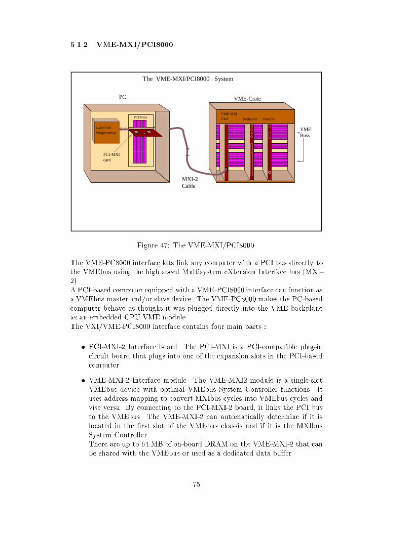
5.1.2 VME-MXI/PCI8000�������
�������
���
���
�������
�������
���������
���������
���������������������
���������������������
��������������
��������������
������
������
��������������
��������������
���������������������
���������������������
���������
���������
���������������������
���������������������
���������������������
���������������������
���������������
���������������
������������������������������
������������������������������
The VME-MXI/PCI8000 System
VME-Crate PC
PCI Buss
Cable
VMEBuss
MXI-2
ProgrammingLabVIEW
Card Sequencer Sirocco
PCI-MXIcard
VME-MXI
Figure 47: The VME-MXI/PCI8000.The VME-PC8000 interface kits link any computer with a PCI bus directly tothe VMEbus using the high speed Multisystem eXtension Interface bus (MXI-2).A PCI-based computer equipped with a VME-PCI8000 interface can function asa VMEbus master and/or slave device. The VME-PC8000 makes the PC-basedcomputer behave as thought it was plugged directly into the VME backplaneas an embedded CPU VME module.The VXI/VME-PCI8000 interface contains four main parts :� PCI-MXI-2 Interface board. The PCI-MXI is a PCI-compatible plug-incircuit board that plugs into one of the expansion slots in the PCI-basedcomputer.� VME-MXI-2 Interface module. The VME-MXI2 module is a single-slotVMEbus device with optimal VMEbus System Controller functions. Ituses address mapping to convert MXIbus cycles into VMEbus cycles andvise versa. By connecting to the PCI-MXI-2 board, it links the PCI busto the VMEbus. The VME-MXI-2 can automatically determine if it islocated in the �rst slot of the VMEbus chassis and if it is the MXIbusSystem Controller.There are up to 64 MB of on-board DRAM on the VME-MXI-2 that canbe shared with the VMEbus or used as a dedicated data bu�er.75

� MXI-2 Bus. The MXIbus is a general-purpose, 32-bit, multi-master sys-tem bus on a cable. The MXI-2 expands the number of signals on astandard MXI cable by including VME-triggers, all VME interrupts andall of the utility bus signals.� NI-VXI software media for the PCI-MXI-2. NI-VXI bus interface soft-ware for Windows 95 is a fully 32-bit native Plug and Play driver forWindows 95. Only 32-bit applications can be run with this driver. Thesoftware includes a Resource Manager, graphical and text-based versionsof an interactive VXI resource editor program, a comprehensive library ofsoftware routines for VME programming, and graphical and text-basedversions of an interactive control program for interacting with VME.These modules are set up as shown in �g. 47.The RESMAN (RESourse MANager) program con�gures the VME-MXI-2 toallow the PCI-MXI-2 to access devises in the VME chassis. RESMAN does notcon�gure the VME devices. However, it is recommended that the informationabout the VME devices is entered into the VXIEDIT utility. RESMAN can thanproperly con�gure the various device-speci�c VME address space and VMEinterrupt lines. The PCI-MXI-2 interface module must have the logical addressof 0.After RESMAN has detected and con�gured all VME the devices, we can viewspeci�c information on each device in the system by using VXIEDIT utilities.These utilities include a Resource Manager Display, which contains a descriptionfor each device. We can interact with the VME devices by using the VICor VICTEXT utilities. These utilities let us interactively control the VMEdevices without having to use a conventional programming language like C orLabVIEW.We used the National Instruments LabVIEW application program to ease theprogramming task. LabVIEW match the modular virtual instrument capabilityof VXI and can reduce the VMEbus software development time. LabVIEW is acomplete programming environment that departs from the sequentially natureof traditional programming and features a graphical programming environment.Further description of this program can be found in LabVIEW section.At every power-up of the VME crate or/and the PC machine equipped withthe PCI-MXI, the PCI-MXI and the VME-MXI have to be initiated. This isdone by running RESMAN and VXI-init program (Ref. [25]).5.2 LabVIEWLabVIEW is a program development application, much like C or BASIC. How-ever labVIEW is di�erent from those applications in one important aspect.Other programming systems use text-based languages to create lines of codes,while labVIEW uses a graphical programming language, G, to create programsin block diagram form. 76

LabVIEW like C or BASIC, is a general-purpose programming system withextensive libraries of functions for any programming task. LabVIEW includeslibraries for data acquisition, GPIB, and serial instrumental control, data anal-yses, data presentation, and data storage. LabVIEW also include conventionalprogram development tools, so one can set breakpoints, animate the executionto see how the data passes through the program, and single-step through theprogram to make debugging and program development easier.5.2.1 The LabVIEW programsLabVIEW programs are called virtual instruments (VIs) because their appear-ance and operation can imitate actual instruments. However, VIs are similarto the functions of conventional language programs. A VI consists of an inter-active user interface, a data- ow diagram that serves as the source code, andicon connections that allow the VI to be called from the higher level VIs. Morespecially, VIs are structured as follows :Front panel. This is the interactive user interface of a VI. It simulates thepanel of a physical instrument. The front panel can contain knobs, pushbuttons, graphs, and other controls and indicators. One enters data usinga mouse and keyboard, and then view the result on the computer screen.One can add controls and indicators to the front panel by selecting themfrom the Controls palette. For doing that the right tool must be selectedfrom the Tools palette.Block diagram. The VI receive the instructions from this diagram, which weconstruct in G. The block diagram is pictorial solution to a programmingproblem. The block diagram is also the source code for the VI. One con-struct the block diagram by wiring together objects that send or receivedata, perform speci�c functions, and control the ow of the execution.The objects are selected from the functions palette.Hierarchical. VIs are Hierarchical and modular. We can use them as top-levelprograms, or as subprograms within other programs or subprograms. AVI within other VI is called SubV I . The icon and connector of a VI worklike a graphical parameter list so that other VIs can pass data to a subVI.With these features, LabVIEW promotes and adheres to the concept ofmodular programming. We can divide an application into series of tasks, whichcan be divided again until a complicated application becomes a series of simplesubtasks. One build a VI to accomplish each subtask and then combine theseVIs on another block diagrams to accomplish the larger task. Finally, we havetop-level VI contains a collection of sub VIs that represent application functions.77

Each subVi can be executed by itself, apart from the rest of the application,which make debugging much easier (Ref. [26]).5.3 Software setupTwo di�erent programming tools were used in the test setup. The programsfor the VME modules was made both in C programming language and in Lab-VIEW. The C programs were executed on the VME CPU called Nitro40, andthe LabVIEW programs used the PCI-MXI/ VME-MXI interface for the datainput/output to the VME crate.A PC machine was used as console or terminal for the Nitro40. A FasTrakprogramming package was used as Ethernet-interface between the PC and theNitro40. FasTrak for Windows development environment is an easy-to-use tool-set for compiling, running, debugging, and updating programs for the OS9operative system. FasTrak for Windows features a Graphical User Interfacepresentation of the Microware Ultra C compiler and Source Level Debugger.Commands and options a�ecting how programs are organized, debugged, andexecuted are selected from windows and menus and speci�ed in dialog boxes.Programs may be created using any text editor, word processor, or desktoppublisher and saved in ASCII format for use with FasTrak for windows.5.3.1 Software under OS9A C-language program for the Sirocco module was made. The Sirocco modulehas control lines, 24 address lines and 16 data lines. Data transfer to the Siroccomodule can only be done in 16 bit mode. The instruction Cache and data cacheof Nitro40 support just 32 bits data transfer (�g. 46) to the VME crate.This problem was found when executing of the Sirocco program, as data transferof 16 bits gave bus error. There is a cache control include �le under Os9 system.This �le contains the routines for enabling/disabling the instruction- and datacache. All the caches must be ushed and turned o� before any communicationwith this kind of VME module.The caches have to be ushed and disabled before any other I/O operation inthe program, such as writing to the screen. After that the module must getaccess to the VME standard memory space.The steps in the sirocco.c program :� First a short type (16 bits) pointer is set to point at the base-address ofthe Sirocco module. Short type pointers are declared for all the Siroccoregisters. Other variables are also declared.� Before any operation in the program, the cache is ushed and turned o�.78

whi
le i
< n
umbe
r of
req
uire
d ev
ents
.
registers.
Set the Siroccobase-address andthe address of
Set DAC base line.The DAC base line regulates the range ofthe ADC converter.
Turn of the instruction- and
EXIT
data-cache.
Get permission for memory access.
Disablethe Sirocco.
Initiate the Sirocco :
the lemo mode, external/internal clock.Set the number of strips to convert, number of pulses to skip before conversion,
Select :n : Read a given number of events.c : List the sirocco memory.t : Test the sirocco by writing/reading to it’s memory.b : List the adc-counts from the buffer.d : Change the DAC base-line.e : Exit
List the Sirocco memory.
Test the Sirocco.
List the adc-countsfrom the buffer
Change the DAC base-line.
Convert enable(Starts theconversion)
Wait for end-of-convert
Stop the conversion.Read the required number of convertedvalues (adc-counts)from the memory
a buffer.and add them in
Read the adc-countsfrom the buffer andsave them into a file
n
ct b d
Figure 48: Sirocco.c ow diagram.� Permission to the VME memory-standard-space is necessary before anycommunication with the VME module.� The Sirocco is initiated. Before the initialization, the ongoing (if any)conversion must be stopped, i.e disable convert. In the initiating step,the Sirocco registers are set such that :(1) Sirocco skips four clock pulses before it converts all the required 256strips. 79

(2) For synchronizing the Sirocco module with the front-end electronics,the Sirocco must start the conversion by the same trigger as the triggerto the Sequencer. It is called Lemo-start. The trigger is feed to the lemoinput of the Sirocco.(3) The conversion is set to be use an external clock, this clock is generatedby the Sequencer (as the rest of control signals for front-end electronics.(4) The range of the ADC converter must be set (The DAC base-line).� After the initialization an 'event loop' is entered. There exist many facil-ities in this loop :(1) In the �rst step of programming the Sirocco, we needed to know thatthe Sirocco really works. This can be checked by writing some data intoit's memory, reading it back and comparing.memory area of the Sirocco, have to be the same.(2) Every read adc-count is stored to a bu�er before writing them to a�le. This bu�er can be displayed if necessary. Some times it is nice tocheck the adc-count values before appending them to a �le.(3) The conversion range of the ADC can be changed by changing theDAC base-line.(4) Speci�ed areas of the Sirocco memory can be displayed.(5) The desired number of events can be converted. This is done in aconvert loop. The adc-counts, for desired number of events ,are storedinto a given �le. The �le format is shown in �g. 49.The clock for the conversion is fed to the J1 connector at the Sirocco's frontpanel. The clock must be turned on at the same time as the analog values, thepedestals for each channel, is avaliable. It is importent that the Sirocco-clocklevel shifts in the middle of each pedestal. This will give the best convertedvalue of the pedestals. The Sirocco clock is also shown in the �g. 58.An sequencer program for the Os9 operative system existed allready, madeby Bj�rn Magne Sundal. This was used to program the sequencer to give thewanted sequences.5.3.2 Software under LabVIEWA LabVIEW program version was made to control the Sirocco VME module.The sirocco VI program is divided into two diagrams, like every other LabVIEWprogram. First is the Front panel, which functions like an user interface. Thesecond is the Block diagram were all the functional information is put.The front panel. The Front panel of Sirocco-LabVIEW program is shown in�g. 50, and the Block diagram is shown in �g. 52. In the front panel,there is possibility to set the DAC base line, the number of pulses to skipbefore conversion, and the number of events to read. It is also possible tocheck the Sirocco memory, by a switch. It is done in the same way as in80

510514480503
477450
550
450
CH#2CH#1
CH#3CH#4
CH#n
477
Event 1
Event 2
510524
510
514
Event i
ASCII formatfile.
Figure 49: The adc-count �le format.the C-program for this module. A value is set into the memory, afterwardthe same memory area is read. If the read values are the same as thewritten values, then there is contact with the Sirocco module.The base address and the registers of the Sirocco are displayed on theindicator. Successful contact with the module is indicated by lights. Byhaving the switch in the convert mode, the desired number of events willbe converted and stored into a given �le with speci�ed format. The �lename is entered in the 'Path controller'. The event number is displayedon a digital indicator. A graph display the converted values in adc-counts,the adc-counts are given in mV on an indicator. A light will ash duringconvertion. The latest memory address is also displayed in a digital indi-cator.The Block diagram. This diagram contains instruction of the base addressof the Sirocco, address of the registers and all the data that have to beset for initializing and reading the Sirocco.The programs is organized in �ve main sub-diagrams, called sequencestructures, or sheets. The Sirocco is disabled in the sub-diagram on 0th.sheet. On the second and third sheet, the Sirocco is initiated. The Lab-VIEW have VXI interface nodes, among these nodes is the 'VXIn' and'VXIOut' node (�g. 51). The nodes, which are written in the conventionallanguages like C, can be used for communication between the VME mod-ules and the PC.The functions of all the di�erent sub-diagrams are explained in the �g. 53.81

Figure 50: The Front panel of the Sirocco programVXIin
VXIout
Accessparm
Address
Width
U16
Status
Accessparm
Address
Width
Value
Value
Status
VXI
VXI
Address : The address of the place to write into.
operation.Status : Indicate the success of I/O
Value : Read /Write 32 bit.
Width : Number of 16-bit package.
Accessparm : Type of access (Read, Write, Execute)
( Inside the VME module)U16
U32
U16
U32
U16
U16
U32
U16
U32Figure 51: The LabVIEW VXI-Interface Nodes.The adc-counts are stored into a �le with the same format as the adc-count�le made by the sirocco.c program. This is done to keep the same adc-count interface to the analyzer program, 'analyzer.s'.There exist a LabVIEW program for the Sequencer module, this is madeby Shawn Roe at CERN. 82

Figure 52: The Block diagram of the Sirocco programsirocco.vi
Sirocco Base addr.
The DACbase line
Number of pulses toskip
# Events to convert
The file nameof where tostore the adc-counts
The fileformat
Store the adc-counts into a file.If test Sir. mem.
selected.The value to
is
write.
Initiating Sheet 0 : Disable the ongoing conversion, if any.
sheet 1,2 : Set the registers. Light on if succesful
Sheet 3,4 : read the registers Light on if succesful
Sheet 5 :
Sheet 1 : Write to Sirocco memory
Sheet 2 : Read from the Siroocco memory Light on if succesful
Light on if succesful Sheet 0 : Convert disable
Sheet 0 : Convert enable (Start the conversion) Sheet 1 : Wait for end-of-convert. Sheet 2 : Convert disable Sheet 3 : Read the 256 converted values
in an array. from the sir.mem., and store/append them
Test theSir. mem.
Convertthe signal
TRUE
FALSE
Number ofevents
Light on
Figure 53: The sub-diagrams sheets in the Block diagram.83

6 The lab system. Test setupsThe �rst step in the test procedure was to measure the noise from the front-endelectronics.6.1 Hardware setupThe following units were used in the test setup (�g. 57).� Hybrid with two FElix32 chips mouted on it.� Support PCB for the hybrid. The PCB is a interface between the hybridand the Sequence.� Sequencer� Sirocco. This VME module converts the analoge signals from the front-end electronics into digital signals.� The Levelshifter. This PCB, made by Bjorn M. Sundal, converts the ECLlevel signals to CMOS signals. The front-end electronics functions withCMOS level signals.� Gain adjust module.� Pulse generator. It generates TRIGGER signal for the Sequencer.� VME crate, with the operative system.� Voltage supply unit.The hybrid is connected to the PCB through the capton cables. A power supplyunit are used for the front-end electronics. The sequencer is used to generatethe control signals, and a level shifter is used to convert the ECL level signals toCMOS level signals. The TRIGGER for the Sequencer is generated by the pulsegenerater. The analoge signals from the front-end electronics are converted intodigital signals by an ADC called Sirocco. The DC level of the analogue signalshave to be inside the converter range of the Sirocco module (described in theSirocco subsection). The DC level of the analog signals are adjusted with theGain Adjust module, before they are sent to the Sirocco. The Sirocco modulestore the adc-counts in it's memory before they are read by a program.The memory of the Sirocco module will be �lled up very rapidly, in a time of614.25 �s (We use a sequence from the sequencer which is 150 �s long and thememory of the Sirocco contains 4095 Adc-counts). Since Sirocco has limitedmemory area, we must read the Adc-counts out from it periodically and storethese data into a �le. A signal from the sequencer is used to synchronize theSirocco with the out-coming data The adc-count �les are then transported to84

file to an UNIX terminal forfurther analyses.
Transferring the adc-countelectronics and the data
VME crate
readout.
Control of the front-end(1)
(2) Control of the VME modules,and the storage of adc-countsinto a file.
(3)
Front-endelectronics
VME CPU and the modules
(2) (3)
UNIX terminal forthe data analyses
(1)
PC terminal to control the
Figure 54: The elements of the test-setup.the UNIX workstation for further analyses. (Fig. 57).The signals, the digital electronics makes, can have di�erent levels. What thelogical signal 'high' and 'low' is depends on the electronic unit. In the lab, theelectronic units required a speci�c kind of signals. There exists, NIM, CMOSand ECL level signals ( 4).Table 4: The logical signalsSignal High LowCMOS � +2.0 V � -2.0 VNIM � -0.9 V � -1.8 VECL � -0.8 V � -0.3 V6.2 Testing stepsBefore any data are read out from the FElix, it is important to check thatevery part of the FElix chip is working normally. First the analog part must bechecked, there is no need for the digital signals in this procedure. The digitalsignals are needed when the functionality of the digital parts of the front-endelectronics are tested. The BIAS currents set in the lab test setup can be foundin table 5.Note that all the bias currents written in this section are given for both FElixchips, and both MUX chips.The voltage Vfp, for the feedback resistor in the preampli�er, is set to -0.25 V.The voltage Vfs, for the feedback resistor in shaper, is set to 0.30 V. All thesevalues are set by potensiometers on the PCB.85

Table 5: The bias currentsFElixPREB 1035 �ASHAB 230 �ABUFB 100 �AAPSPB 40 �AMUXBUBI 300 �ASFBI 40 �ABy applying a step-pulse into CAL test-input, there must be a perfect CR-RC shaped pulse out of �rst broken channel OUT1, called OUTAMP11 andOUTAMP21 on the PCB. This pulse should have a peaking time of 75 ns. Aftersetting the analoge signals, an approximately perfect CR-RC pulse is locatedat the �rst broken channel (Fig. 56). This indicates that the analog parts ofthe FElixes are functioning well. The height of the shaped pulse is proportionalto the value of the step-signal to the CAL input of the FElix. With the givenBIAS currents, Vfp and Vfs the ampli�er got into saturation at � 7 MIPs (448mV).All the data read from the front-end electronics are read from the second DTAgroup. The available data in the �rst DTA pulse is found to be garbage data.The numbers of the DTA pulses can be controlled by the width of the �rst leveltrigger, T1(table. 6). Table 6: DTA pulse vs. width of the T1T1 (ns) 100 300 400 450DTA groups 1 2 3 4The digital part of the FElix chips was tested by applying the digital signals.To get the FElix chip to work, it must be applyed with the right sequence ofthe control signals. The FElix chip must be reset at every sequence cycle. The�rst level trigger , T1, must arrive at the correct time. The BUSY signal of theFElix must not be set throughout the readout cycle. When the digital part ofthe FELix, is �nished with the data handling, there will be sent a DTA signalon the FElix output. The DTA was observed, this indicates that also the digitalparts is functioning.The output bu�ers, sample and hold unit of the MUX must be fed by the biascurrents to operate. (Note that all the bias currents written in this section aregiven for both the FElix and the MUX chips). The sequence used in the testsetup is shown in �g. 58. The easiest way of reducing the e�ects of inductivecoupling to an external interference sources, is to have each power line twisted86

Figure 55: The �rst broken channel.Figure 56: First broken channel, zoomed.with a ground line into loops of approximately equal area. The magnitude ofthe interference voltage induced in a loop is canceled by an opposite voltagemagnitude induced in the next loops. In this way the electro-magnetic noise inthe conductor loops, in the PCB and the hybrid, is reduced.In the lab there is two hybrids with old logic FElixes, and a detector is bondedon both of these hybrids. There is also two hybrids with the new logic FElixes,without the detectors.6.3 The noise from front-end electronics with the detectorIn this test setup we used the hybrid with old logic FElixes with a detectorbonded to the FElix inputs. The detector have a strip pitch of 25 �s and a 50�s readout pitch. The detector is of size, 3 cm x 6 cm with a strip length of 6cm, the thichness is of 350 �m. The detector have p+-strip and n-doped bulk.Before any data readout for the noise measurement, the front-end electronics87

B30
Pulse generater
Level shifter
Power supply
Sequencer
Sirocco
Gain adjust module
PC-terminal (DOS)
support hybridFElix32
MUX
Tr
Clk
B29 Tr (In)
(Signal Input)
In Out
DC
(For controlling the VME modules)
Out
CAL
INP1 2
Mout1PCB
FElix32
0 V
+ 8 V0 V
- 8 V
+ 2 V0 V
- 2 V0 V
8 V
2 V
Controlsignals
UNIX terminal(For the data analyses)
503506480530502512
Telescope
NIM Crate
VME-Crate
Nitr
o40
AC
Figure 57: Test Setup.88

The idle loop is 20 units long.
FElix signals
BCO
Reset
Busy
Reset
Read Bit
Hold
Clk
MUX signals
Sirocco
Trigger
Clk
(T1)TriggerFirst level
16
Typically #1100 wide
812
12
390
10
40
12
12
32 cycles
< 20 >
< 20 >
6500
6300
97
320
330
408 436(Peak Mode)
(De-conv.)
260 cycles 727
Time(# x 25 ns)
Peak mode
Mux clk
Sir. clk
90 degree phase difference.Length of sequence is of about 7000 units.Figure 58: The control signals for the test setup.must be well shielded from electro-magnetic noise. It is done by placing thefront-end electronics in a totally shielded iron box. In such way the electro-magnetic noise is reduced to minimum. For data taking the front-end elec-tronics is supplied by the sequence shown in �g 58. Both the noise in peak-and de-convoluted mode were measured. The data was read from the Siroccoand stored into several �les with 500 to 600 events. This data was analyzedby the analyzer program and analyzed graphically in PAW by the student JanSolbakken.The de�nitions are :The common mode noise , �cm, is the RSM (standard deviation) of the varia-tions in the DC level of all the channels.The parameter, �, is RSM of the pedestal distribution of each channel.89

������������
����
����
������
����������
��������
��������
������������������������������
DetectorCALINP1
MOUT1
MOUT2
PCB HYBRID
+8 V -8 V
-2 V+2 V
0 V
0 V
Vbias(detector bias)Figure 59: Front-end electronic shielding.Table 7: The noise performance of the FElix32Noise (�V) Common mode (�cm) pedestal (�) Pedestal RSM(�cms)Peak mode 670 1410 1240De-conv. mode 1100 2520 2270The parameter, �cms, is the RSM of the changes in pedestal value of each chan-nel after subtraction of the common mode noise. There was big noise problemsin the lab, we had lot of problems with the common-mode noise. The commonmode noise is related to the noise from the power supply lines of the front-endelectronics. Compared to 1 MIP (64 mV) the common-mode noise is very high.The common-mode noise can be subtracted in software. The measured noisevalues in the lab, is more than accepted. These can be explained by that themeasured values above, is for the FElix chips with no detector bonded on it.The measured noise is the noise from the FElix plus the noise from the detector,or :noise2 = noiseFElix2 + noisedetector2 The detector is not feed by any voltagesupply. This is same as that the FElix channels are connected, to a capacitiveload, or some antenna, that cache noise from the surroundings.After the de-convolution the noise value should be increased by a factor 1.8,compared to noise for the peak mode. This is veifyed by the results.90

6.4 The CAL test methodThe CAL test setup is same as the setup shown in �g. 57. The CAL step pulseis made by a pulse generator. The trigger which is used for the Sequencer mod-ule, is also used to synchronize the CAL signal with the front-end electronics.How this is done is shown in �g. 60.We used CAL test-input to �nd the delay between �rst level trigger, T1, andPulse generator
Out
TR
Trigger In
VMEmodule
Sequencer
Trig.
LevelShifter ECL
CM
OS
(Lemo plug U21 of the PCB).To the CAL input of FElix Sequence to
the front-endelectronics.
Pulse generatorOut
Trigger Out
CAL
TR
Figure 60: CAL Test Setup.the CAL signal. This delay can be calculated. There is 84 cells in the FElixpipe line and 67 of these cells are used for delay of the CR-CR pulse. TheBCO clocks the samples from one to next cell. The peak value of the CR-RCpulse will be in the last cell after delay of 67 � 25 ns = 1675 ns. If the digitalpart of the FElix is in order, all channels will be maximum exited at the righttiming of T1, or at the delay of 1675 ns between CAL pulse and T1. Betweenthe CAL-input and each FElix input, there is a capacitor of 56 fF. With thiscapacitor, one Mip corresponds to qC = 22000e56fF = 63 mV (�g. 61).The method used in the CAL test setup, is to hold the �rst-level-trigger at a�x delay after the trigger TR. After that, change the delay between the T1andthe CAL signal. The delay is changed in a step of 25 ns. A step signal of 3Mip (190 mV) was used for CAL to sample through the CR-RC pulse in thepipeline. An maximum excitation of all channels was seen at a delay of 1500ns, between CAL and T1, while, 1675 ns was calculated. There was a drop of80 mV in the level with a 3 Mip step signal.The second measurement was to �nd how the DC level changed. Several smalldelays in the system might account for the di�erence, as a function of the inputsignal. We held the delay between T1 and the CAL signal at 1500 ns. Thevalue of CAL signal was increased, 0 - 8 Mip, to �nd the drop in the DC levelpr. MIP. The CAL signal was increased with steps of 1 Mip (Fig. 61, 66). Thecommon mode noise and the RMS of pedestals vs. number of Mips is measured91

cal
1 Mip = 64 mVC cal = 56 fF
C
A detector strip of the detector used in the lab test setup.
TR
T1
CAL
> 10 ns
Delay
6450 ns
# of MIP
Pipe line (84 cells, 67 cells are used for delay)
Pre-amlifier Shaper
1675 ns
CAL
V bias
Detector, if any.Figure 61: First level trigger compared to CAL step-signal.(Fig. 68). The result is discussed in the next section.Data with many events have been taken in the CAL test. The whole CR-RCpulse in the pipeline have been 'scanned' by di�erent delays between the CALpulse and the T1 (Fig. 61). The collected data have been stored in several�les. A program in C ('analyzer.c'), was made to analyze the data. In this pro-gram, many interesting parameters like, pedestals, the noise in the pedestals,the common mode noise etc., are calculated. This desired parameters can bestored into a �le for further analyses in the graphical analyzer program PAW.The sampled CR-RC pulse (Fig. 67) is drawn in PAW.6.5 Source setupThe main goals of this setup was :(1) Measure the noise performance of the detector.(2) Collect the hits by radiating the detector.(3) Find the signal to noise ratio.The setup is the same as in �g. 57, now the detector is also feed by the biasvoltage. In the �rst test, to measure the noise performance of the detector, thedetector is not radiated by any source. The detector performance was measuredby changing the detector bias voltage. For the detector used in this setup, posi-tive bias voltage (V bias > 0) is needed to depletion the detector. By increasing92

Figure 62: Detector noise vs. the bias voltage.(V bias > 0) the deplete zone of the detector zone will increase, this will result adecrease in the noise from the detector (as discussed in the detector subsection).Fig. 69 shows the noise performance of an ATLAS-A detector, the depletionvotage is around 25 V. After full depletion of the detector, there is very littlefall in the noise. As seen in the �gure, the noise in the peak-mode is less thanfor the de-convoluted mode. The collected data for di�erent voltage steps, isshown in �g. 69. The �gure shows the noise from the detector strips. Thestrips, 0, 1, 13, 30 and 31 are not taken in account. These strips seems to bedead, the noise performance for these strips compared to the rest of the stripsis shown in the �g. 69. The results will be discussed in the next section.The next step was search for hits, by radiating the detector. The setup is thesame as in �g. 57, with a di�erence in the trigger logic (�g. 63). A '�nger'scintillator is used to make the trigger, TR. The power supply to this scintillator93

should not exceed 1200 V, or 1.2 V at the input of the ampli�er. The ampli�erhas a gain of a thousand. The trigger logic is shown in �g. 64.The folowing steps are necessary to create a trigger, TR.(1) As seen in the �g. 70, the signals from the scintillator can not be used totrigger the sequencer. The signal must be converted into NIM level, widerthan 10 ns, before they can be used for triggering the front-end electronics.The signal SCINT, is the signal from the scintillator. This signal has beenampli�ed, to � - 800 mV, by using the Timing �lter ampli�er module.In the next step the integrater constant, � , have been decreased, so thepulse is now wider, SCINTB.(2) We need the inverted of this signal, SCINTC . It is taken from the invertedoutput from the same module, Timing �lter ampli�er module. This signalis not exactally the inverted, but the 're ected' signal of SCINTB, thisis 're ected' around 0 mV.(3) The next step is to convert this to NIM again. This is done by the Gainadjust module. The DC level of this signal is simply lowered to the NIMlevel, the SCINTB .(4) The signal,SCINTNIM , is the same as SCINTB, but it has the right NIMshape. This signal can now be used as a trigger for the sequencer.There is a problem with the SCINTB signal, the width of the pulse will os-cillate, with oscillating positive edge (the active edge). The reason is that thepulses from the scintillator have di�erent widths and heights. The second prob-lem is, that several pulses from the scintillator will arrive within the readoutcycle. This will results that the sequencer is triggered again before whole read-out cycle is �nished. These problems can be cured by making a new trigger,TR. How this is done, is shown in �g. 64 c. The trigger, TR, is an AND be-tween the the SCINTB signal and a signal called B30. The B30 is a signalfrom the sequencer, this arrives, with other control signals, at the output ofthe sequencer. This happens at the �rst positive edge of SCINTB. The nextSCINTB signal will not be accepted until the B30 is brought high again. TheB30 signal is programmed to be low at once the trigger is arrives, and it isbrought high again at the end of the sequence. In such a way, the unwantedtriggers can be blocked.There was no AND NIM module in the lab, so the technic shown in �g. 64 dis used.The �-sources used in the test-setup :Ru106;44 1.5 MBq, Energy = 3.500 MeV, (From Feb. 87, half time of 378 days)Co60;27 Energy = 0.32 MeV , (From Aug. 74, half time of 5.272 years)The detector was supplied by a bias voltage of 130 V. In silicon one gets anelectron-hole pair for every energy-loss of 3.6 eV released by a particle crossing94

(to the Sirocco)Front-end electronics
Detector Bias (V )b
Supply voltage (V )s
Scintillator
Scintil
lator
pulse
s Trigger logic Sequencer
TR
B30
Controll signals
Mou
tThe analog valuesFigure 63: Source test setup.the media. The � particles (electrons) of the sources are relativistic and willbehave as MIP's. As mentioned in the section of detectors, the average energy-loss in the detector is about 290 eV�m , the detector in the test setup is 350 �mthickh, this will give 290eV�m �350�m3:6eV = 28 194 electron hole pair.The trigger logic has a delay of � 50 ns, it means that there is a delay of �50 ns between the active edge of the SCINTB pulse and the trigger TR. Withthis delay the �rst level trigger, T1, has to arrive � 50 ns earlier than thecalculated delay of pipeline of 1675 ns. The found delay was of 1500 ns. Thedata was collected by varying the �rst level trigger between 1400 - 1700 ns. The'analyzer' program was used to �nd the interresting events. By looking at thestrips-signi�cases of the collected data, which was symmetric around 0 V, onecould conclude that there were no hits at all (�g. 65). The further analyses ofthese data will be done in the next section.6.6 New logic FElix32In this version of the FElix, we found a delay of 1500 ns between CAL and �rstlevel trigger,T1. It is the same as the delay found for the FElix with the oldlogic. Some problems with the DTA pulse was found. DTA is generated by theinternal clock of ASPS. DTA was oscillating with a period of 800 ns. After 800ns it jumped to the initial position. Some times the DTA moved forward veryrapidly and created di�culties with data taking in Peak- and De-convolutedmode. The HOLD signal on the Mux had to be activated in the Peak- De-convoluted time of DTA, to test in these modes. The DTA pulse was not �xedin time compare to the Mux HOLD signal. This problem occurs because thisFElix chip has a continous APSP clock. When a �rst level trigger (T1) arrives,it does not hit the active edge of the BCO clock, this results a delay of 25 nsfor the DTA. This happens at every T1. The APSP's clock runs at 1.25 MHz,95

sµ 600
SCINTB
SCINTA
SCINT
SCINTC
SCINTNIM
TR = TR = SCINT + B30
TR = SCINT * B30
TR = SCINT * B30
TR = SCINT+ B30
By De Morgan’slaws
NOR
AND
TR TR
SCINT
B30SCINT
B30
(4)
TR
= SCINT & B30
150 mV
0 mV
0 mV
-800 mV
0 mV
1.5 ms
-800 mV
0 mV
0 mV
800 mV
0 mV
-800 mV
-800 mV (NIM level)
Timing filter amplifier module module
ORadjust moduleGain
Out
In In
Out
In
Out(a) B
A
(b)
(d)
(c)
TR
Scint
1
0
Oscillations
SCINT
(c)B30
(d)
Fig.c
Fig.d
A B AND A B NOR
0 0 0 1 1 0
0 1 0 1 0 0
1 0 0 0 1 0
1 1 1 0 0 1
0
1
Fig.bFig. a THE TRIGGER LOGIC
NIM level : High : -800 mVLow : 0 mV.
SCINT B
(1)
(2)
(3)
Figure64:Thetriggerlogic.thisgivetheperiodof800ns.Afteradelayof800ns,theDTAbeginanew
96

Figure 65: The strip signi�canse, peak mode.period from start.This problem can be resolved by generating the Mux HOLD signal from theDTA pulse, then the HOLD signal will appear at the same time inside theDTA. This will demand more external electronics, and is not feasible in the testsetups.The DTA pulse in the NEW FElix chip ocillated so rapidally that we couldn'tmake any CAL test on it. The only data we collected, before the sample signalfalled out of DTA, was the noise mesurement data. The noise performance isgiven in table.Table 8: The noise performance of the new-logic FElix32Noise (�V) Common mode (�cm) Pedestal (�) Pedes.(�cms)Peak mode 547 818 59097

Figure 66: Drop in the DC level pr. mip.Figure 67: The sampled CR-RC pulse.
98

Figure 68: The Common mode noise vs. Mip, and the channel noise vs. Mip.
Figure 69: The channel noise vs. Mip.99

Figure 70: The pulses from the Scintillator.100

7 The analyses of data, PAW, KUMACThe data from di�erent test setups is collected for further analyses :� The setup for measuring the pedestal noise, common mode noise.� The CAL test setup.� The setup for detector performance.� The source setup.Pedestal Rsm
Adc count data file read from sirocco
PAW Graphic Display of
Adc count Distribution
C program
analyzer.c
Distribution
Distribution
Distribution
EventLook at one
Hit Significanse Distribution
DistributionStrip Significanse
Distribution
DistributionCluster size
Hit Significanse
Strip Significanse
Cluster size
file
file
Adc count file
Adc count file
Hit Significanse Histogram
Strip Significanse Histogram
Cluster sizeHistogram
AndMuch More
Common modeDistribution Distribution
Strip Noise
UnixWork
Pedestalvalues
Station
Pedestal
Pedestal RsmFigure 71: Analyzing the data.All the adc-count �les written on the VME system is transported to UNIX andform the basis for further analyses.7.1 PAW, KUMACPAW , The Physics Analysis Workstation, is used to analyze the event data.A self made program, analyzer.c is also used to calculate di�erent parameters,like variance in common mode noise, the strip noise, signal to noise ratio andmake histograms. This program can �nd which strip is not working, and canidentify hits. 101

7.2 The methodsThe adc-count data is raw data read from the detector via the front-end elec-tronics, FElix32. To read these data we use a module called Sirocco. Analogsignals from the detector are sent to the Sirocco, this module converts thesesignals to digital signals. Sirocco is sitting in the VME crate and is programmedfrom the OS9 system. The adc-count data can be data from the front-end elec-tronics with or without the detector.If we take the performance of the front-end electronics without the detector,then all the noise coming from the electronics is found. It is noticed that theperformance of the front-end electronics is strongly linked to the variations onits bias power supplies. There are two main type of noise.� Common mode noise.This noise is made by front-end electronics power supplies and is thevariation or the standard deviation in the DC level of the signals comingfrom all the di�erent channels in the FElix. When calculating this noiseit is important to omit the dead channels, if they exist. Common modenoise can be subtracted from the signals by essentially averaging overthe channels. The DC level of all channels will then be zero. After thecommon mode noise subtraction there remains just the pedestal noise ineach channel. The data after the subtraction is called the common modesubtracted data.� pedestal noise (channel noise).This is the variations in the pedestal of each channel.All the noise has a normal distribution. The noise will increase with the de-tector bonded to the electronics. Some of the detector noise is made by theminority carriers in the non-depleted zone in the pn-junction. This kind ofnoise will decrease by increasing the depleted zone by increasing the bias volt-age. When the bias voltage is supplied to the detector the noise will decreaseby increasing the bias voltage. If the reverse bias voltage is high enough, thenthe detector will be fully depleted and the noise from the detector will be atits minimum. In our setup we used a detector with p+ strips and n-bulk. Thedetector must be fully depleted to have a good performance. The detector weused in the lab setup was a 350 �m thick Foxfet biased detector with 50 �mreadout pitch. The charge released by a tranceversing particle in this detectoris about 80 elec�holepair�m 350�m = 28000 electron/hole pairs.Only 64 strips are read from the detector by two FElix32. When a particle passthrough the detector it will release electrons along it's path. Since the detectoris supplied with bias voltage, there is an electric �eld between the strips andthe bias back-plane. In our detector, the charges moves in the electric �eld andinduses a negative signal on the strips. A particle passing vertically throughthe detector gives a signal on at least one strip. If the particle pass in middleof two strips it will give signal in two strips. A cluster is continuous strips with102

signal, the cluster size is the number of strip in a cluster.7.2.1 The reference data for location of hits� The �rst pass.From the �rst 50 events of the event data, the mean and the standarddeviation or Rms is computed for each channel. This is called �raw and�raw. If there are some hits in these data the raw mean of the pedestalwill increase or decrease depending on the detector type, for our detectorwith p-type strips and n-type bulk the mean will decrease. The raw-dataRms is also increased. These raw values will be to high to be used asreferences to �nd the hits.� The second pass.In this pass the �ner mean and Rms of the pedestal is found for eachchannel from the next 50 events in the event �le. This is done by sortingout the strip data which is greater than � 3 times raw-data Rms aroundthe �raw, it means that we discard the data which areadcvalue� �raw�raw > j � 3jAll data above this threshold from each channel are discarded. For theremaining data, the �ne mean, �fine and the Rms, �fine value is calculatedfor each channel.If needed there can be an third pass by sorting out the data greater than� 3 �fine around the �fine from the next 50 events. We call these for�finer and �finer values for each channel.Because the reference values are calculated out of the same event �le they willbe the best reference values to �nd the hits and clusters in the event data.7.2.2 Hit and Cluster SearchIn each event the impact point of the incident particles on the detector is ob-tained from a strip cluster search that proceeds as follows :1. The strip signi�cance (s = charge collected in this event/noise = (V��)� ) iscomputed for all channels.V is the adc value on the strip.� is the mean of pedestal value.� is the standard deviation, Rms, in the channel.2. Then the primary strip is de�ned as the channel with the highest strip sig-ni�cance if s > 3.3. Those strips within an interval of � 5 strips around the primary strip withs > 3 are included in the cluster.4. The hit signi�cance is de�ned as the sum of the signi�cance of all strips103

included in the cluster.5. The search for more clusters in the same event continues until no strips withs > 3 remains.The signal to noise ratio is taken as the peak of the hit signi�cances distribu-tion, as it compares to the charge collected in one strip with its noise. This isdone for all the strips in a cluster. The cluster is just given by the number ofstrips in each cluster (Ref. [6]).7.3 Self made data analyzer program, Analyzer.c���������
���������
���������
���������
�����������������������������������
�����������������������������������
�����������������������������������
�����������������������������������
������������
����������������������
����������
������������
����������������������
����������
InputAdc count data file
������������������������
������������������������
Strip Pedestal Rsm or mean
sizeCluster
Analyzer.c
Outputs
file.
file.
file
file.
.significance
Hit Significance Figure 72: Analyzer.c7.3.1 The motivation for the programmeA program was made, which without use of PAW, we could calculate manydata like pedestal, Rms value for each channel and the cluster sizes. A programwhich could compute the mean of the pedestal and the variation was needed.It calculates all spesi�c data very easily, and we can design the program tocalculate other features we need to know.When a trigger arrives from a scintillator, the whole setup is restarted, and thedata corresponding to this event is treated by the FElix and the MUX, beforeit is sent to the Sirocco. The adc-values are read from the Sirocco to a �le. This�le is transported to an UNIX work station for further analyses. Each eventcontains 256 adc values, where only the �rst 32 adc values are coming from thedetector channels.We can get false triggers from the scintillator due to electronics noise. To avoidthe data from these false events, some procedures are made in the program,104

that can sort out the false events.Firstly this program read the event data from a �le, and each event get a num-ber, the events number. For the FElix with 32 channels the DC level of eachevent is calculated. The DC level is the mean, � of the values from all the activechannels. The dead channels (strips) are not taken into acount. When calcu-lating the mean of channel n, the over ow and under ow values is not taken incount. The mean value for each channel is used to �nd the noise variance andthe standard deviation.INPUT ; The adc count data �le.OUTPUTs ; There are �ve outputs.� The Strip signi�cance �le.� The Hit signi�cance �le.� The Cluster size �le.� The variance �le with, Rms in all the active channels.� The mean of pedestals for all the active channels.All other outputs are to the monitorAll these outputs can separately be written into �les. Each �le can then befurther analyzed by PAW. The program can also �nd the mean and the mostprobably value for each distribution like the SN or hit signi�cance ratio distri-bution and the pedestal value distribution.105

mean
�����
�����
����
�
�����
�����
����
�
Adc Count data file
RawData
New
File
Display Events.
List someEvents. size
Distribution.
of allEvents
values.over pedestal
Vs.The hits.
Events withpossiblehits.
Events withpossible hitsin detaile.
S/N
Distributions
List the referanses
data.
Histogram
The strips
DC level
Cluster-
common modesubstracted
Raw or
data
computed data Write the
into file.
Save the channel
significances.sizes.
Save the hit
significanses.
Save the Rmsof pedestal
clusterSave the
Hit
distribution.significansesignificanse
distribution.
Strip
Compute the
all events.DC levels of
Find thehighest & lowestDC level.
Find the highest& lowest pedalstall values.
common mode noise& the mean of
Compute the Rms & means of the pedestals from allevents.Display : Max, min values
& the Rsm, means for each pedals.
Find the possible
hits & clusters.
Find the bad
events & strips.
for all pedestals from thefirst 150 events. Use theese
Copute the Rms & means
values as the referanseto find the hits.
Check the calculations.
Compute the Rms
Save the
of pedestalFigure 73: Flow diagram, Analyzer.c106

7.3.2 Steps in the programRead the event data �le. A adc data count �le is read and sorted in eventscontaining 256 adc values, where the number of active channels is 32.Each event is characterized by its event number.Compute the DC level. The DC level of each event is calculated, both forthe active channels and the rest of channels. At the same time the eventswith some strips which have over ow or under ow values is marked asbad events. In the further calculations these bad events is not taken intoaccount.The lowest and highest DC level. The lowest and highest DC level is foundwith the corresponding event number.The lowest and highest pedestal value. The lowest and highest pedestalvalue with the corresponding event number is found for each channel.The Common mode noise. The mean and the Rms of the DC levels arefound. The mean variation in the DC level is called the common modenoise.Strip noise. The mean and the Rms of the pedestal is calculated for eachchannel. The maximum, minimum pedestal and their corresponding eventnumber are displayed. The Mean and the Rms of pedestal for each channelare also displayed.Calculate the reference data. The method described in (chap.5.2.1) is usedto �nd the reference �finer and �finer data for each channel. In thisprogram tree passes are used to �nd these values.Find the hits and clusters. By using the �finer and �finer the hits and theclusters are found by the method described in (chap.5.2.2). The Stripsigni�cance is then calculated.Display the bad events with the number of bad strips. The bad eventswith the numbers of the bad strips are found and displayed. A bad eventis de�ned by that at least one strip in this event has an over ow or un-der ow adc value. A bad strip is de�ned as one strip that always has thesame value, over ow or an under ow in all the events. The Adc converterSirocco gives a channel under ow or over ow value if the analog signalinto the Adc converter is out of the converters range.Hit signi�cance and cluster size. If there are any hits the Hit Signi�cancesand the cluster sizes are computed.Display, All the data can be displayed on the monitor.� Some events with the channels and all the channel data like adcvalue, the charge collected and if hit, the strip Signi�cance for thechannel. 107

� The list of the events with the hits.� The number of the positive and negative hits on each strip.� These events can be displayed in detail.� The list of the reference data, this data is calculated as mentionedin (secttion.7.2.1).� The list of DC level of all events.� Draw a histogram over the DC levels. The peak and the mean of theDC level are also displayed.� The histogram over all pedestal values for a strip. The peak and themean values of the pedestal are displayed.� The cluster size distribution is shown in a table. (Furthermore theprogram will be extended to draw the histogram and display thepeak and mean value of the cluster size. The drawing histogramroutine exist already.)� The strip distribution is shown in a table. (Furthermore the programwill be extended to draw the histogram and display the peak andmean value of the strip distribution.)� The hit distribution is shown in a table. (Furthermore the programwill be extended to draw the histogram and display the peak andmean value of the hit distribution.)All the calculations can be done both for the raw or common mode subtracteddata, CMS data. The CMS data for a channel is just the adc-value subtractedthe DC level of this event.For the calculations with CMS data there is a built-in test in the program. Wecalculate the variance of the Common Mode noise, the variance in the pedestalvalue for all the channels based on the raw-data, and the variance in the pedestalvalue based on the common mode subtracted data. There is a relationship be-tween these variances. This relationship is calculated in the noise relationshipchapter, equation(11). The calculated variances is checked against this equa-tion.If there are no hits in the event data, then the data will just contain the sta-tistical 'hits' out of the � � 3� pedestal range. In this situation 99.97 percentof the adc-values, will lay between this range. If all the strips are functioning,then the sum of the positive and the negative hits be zero. If the detector isradiated and the readout timing is correct, the data should contain much moreof one type of hits. For the detector used in the lab, p-type strips and n-typebulk, there will be mostly negative hits.108

7.4 The noise from the detector.In events with tracks crossing the detector between two strips only a fraction ofthe total charge is collected, but the problem at charge sharing is even more se-rious for tracks crossing the detector at large angles, when the charge is sharedby 3 or more strips.The mean contribution of the noise come from the capacitance of the strips be-ing read out to its neighbors and the backplane. It causes a signal loss and actsas a load capacitance of the pre-ampli�er. These two e�ects can be minimizedby making coupling capacitance high and the inter-strip capacitance small. Formost readout electronics the load capacitance gives the main contribution ofthe electronic noise. For conventional charge sensitive ampli�er the electronicsnoise is calculated as an equivalent noise charge ENC given byENC = A+B � C (3)A, B is constants, C detector capacitance.B depends on the pre-ampli�er.ENC is given as the number of electrons at the input, which would correspondto the observed noise.7.5 The noise relationshipsIn our setup we have two main types of noise. The Common mode noise and thechannel noise. Common mode noise is usually the variation in DC level of allchannels in the events. Since the Felix is sensitive to power supply uctuationsthe DC level for each events will vary. Some times the Common mode noiseis very large, which make it impossible to see a mip signal without Commonmode correction.If we have i events, then the Common mode noise can be de�ned by the stan-dard deviation, �cm, and the mean, cmi of the DC levels.The strip noise is caused by electronics inside the Felix. The strip noise can becalculated in two ways.� With the raw-data for a channel.It is characterized by standard deviation, �raw;n2, where n is the channelnumber, and the mean value, Xn. X is the noise value in channel n.� Using the Common mode subtracted data.After Common mode subtraction, the DC level of each event should bezero. After subtraction all the strips have only the strip noise left. In thisway there is no Common mode noise left in the channels. The channelnoise is characterized by standard deviation, �cms;n2, where n is the chan-nel number, and cms is short for Common mode subtraction. The mean109

of all values on one channel is yn. y is the noise value in channel n minusthe common mode for this event.We have the following raw data from the events.X X X X . . . . . X
X X X X . . . . . X
X X X X . . . . . X
Event i :
. . . . .
. . . . .
X X X X . . . . . X
. . . . .
Event 2 :
1,0 1,1 1,2 1,3 1,n
2,0 2,1 2,2 2,3 2,n
i,0 i,1 i,1 i,3 i,n
3,0 3,1 3,2 3,3 3,3Event 3 :
Event 1 :
Figure 74: Events.The DC level is given by cmi = 1NXn Xi;n (4)where N = n + 1.The mean of the Common mode noise is given bycm = 1iXi cmi (5)The standard deviation for the common mode noise is given by�cm = (1iXi (cmi � cm)2)12 (6)All channels have a bit of noise, the mean of the noise in channel n, is given byXn = 1iXi Xi;n (7)The standard deviation for the channel noise is given by�row;n = (1iXi (Xi;x �Xn)2) 12 (8)Here we have the channel data with common mode subtraction :110

Yi;n = Xi;n � cmi (9)The mean value of the noise for one channel is given byYn = 1iXi Yi;n (10)or Yn = 1iXi (Xi;n � cmi)Yn = 1iXi Xi;n � 1iXi cmiwhich gives Yn = Xn � cmi (11)The standard deviation of the channel noise for an channel with Common modesubtraction is �cms;n = (1iXi (Yi;x � Yn)2) 12 (12)We replace Yn = Xn � cmiand Yi;n = Xi;n � cmi.The equation is then solved to be�2cms;n = �2raw;n + �2cm � 2iXi (Xi;n �Xn)(cmi � cm) (13)This solution can be used to calculate the variance in noise with Common modesubtraction in channel n. For a more general solution we must sum this solutionover all the channels :Xn �2cms;n =Xn �2raw;n +Xn �2cm �Xn (2iXi (Xi;n �Xn)(cmi � cm)) (14)The last element can be written byXn (2iXi (Xi;n �Xn)(cmi � cm)) =Xi [2iXn (Xi;n �Xn)](cmi � cm)and Xn (Xi;n �Xn) =Xn Xi;n �Xn Xn= N � cmi �Xn Xn= N � cmi �N � cm111

The last element is calculated as shown below :Xn Xn =Xn Xi Xi;n=Xi Xn Xi;n= N �Xi cmi= N � cmAnd from (4) we have 1nPnXi;n = cmiFrom (5) we have Pi cmi = cmIn the analyses of the data, we found a relationship between Common modenoise and the channel noise on the FElix. The relationship was found to be(�cms)2 = (�raw)2 + (�cm)2 (15)�cm2 is the variances of the Common mode.�raw2 is mean of the sum over the variance of all n channels.
112

7.6 Results of the data taking.The data collected is analyzed with the analyses program 'analyzer.c' and PAW(by Jan Solbakken).7.6.1 The noise level with or without the detector.There were two hybrids in the lab, both with the detectors. The data collectedis for the FElixes bonded to the detectors.Figure 75: All the channels of the FElix32. In peak mode.The �rst �gure in �g 75 is based on raw data, and the second is based onthe data after common mode subtraction. The �gure shows all the channels ofFELix32. Two events is drawn in the same �g. The channel 23 seems to benoisy. The noise from all the channels was similar, at about 1360 �V, calculatedfrom the raw-data and 1260 �V from the common mode subtracted data. Thenoise in the pedestal is reduced after the common mode subtraction (�g. 76).The common mode noise is shown in (�g. 77). Data in the de-convoluted modewas also taken. The common mode noise was higher in the de-convoluted mode,about two times higher than in the peak mode (table 8). The common modenoise and the pedestal noise, found with the PAW program is similar to thevalues calculated in the 'analyzer' program. The results in the lab at CERN,shows that the noise in the de-convoluted mode is a factor 1.8 higher than forthe peak mode. The results shows that also in our test setup the factor is about2. 113

Figure 76: The channel 23 of the FElix32. In peak mode.Figure 77: The common mode noise. Peak mode and de-convoluted mode.7.6.2 The CAL test setup results.Several adc-count �les from this setup was made. The collected data is :(1) Pedestal vs. the delay between the CAL and the �rst level trigger.(2) DC level vs. number of Mips on the CAL input.(3) Common mode noise vs. number of Mips on the CAL input.The raw data from these setups is input the analyzer program. The selecteddata is sorted, like the pedestal value and added to a �le containing the dataof same set. In this way, all the adc-count �les related to this setup is collectedand added to the same �le. The �le with the interesting data, as in our setupsin points (1-3), is transported to a UNIX workstation. Here they are run in114

Figure 78: All the channels of the FElix32. In de-convoluted mode.PAW, to produce the graphs.An 5 Mip (320 mV) signal was used at the CAL input, �g. 67 shows the sampledCR-RC pulse.The common mode noise increased by increasing the input. �g. 77 This shouldnot happen, the common mode noise made by the FElix chips is constant. Theincrease could be explained by that there is other noise sources close to thefront-end electronics. This could be the pulse-generator that generate the CALpulse. Since all the channels is exited by the CAL signal, there will be anincrease of noise in all channels, in the same way as in the common mode noise.So the increase of noise we see at the channels is probably the increase in noisefrom the pulse generator.In the source setup, the detector was feed by the bias voltage, Vbias, to measurethe noise from the detector with respect to increase of the bias voltage. Theperformance measured is shown in �g. 78, the excepted performance is shownin �g. 69. The detector we used should fully depleted at the bias voltage of� 25 V. In the lab measurement (�g. 78), it can be seen that, in the �rst 5V, the noise from the detector is decreasing as expected. After 5 V it seemsto be fully depleted (some of the detector strips, like strip 13 and 31, seems tobe fractured, these strips seems to increase the noise with respect to the biasvoltage). Since the depletion voltage is about 25 V, it can be concluded thatthe noise measured is a sum of noise from other sources around the setup. Thisnoise seems to be independent of the bias voltage of the detector. At Vbias <5 V, the noise from the detector is dominating. After this bias voltage, thenoise seems to stabilize around 700 �V. Since the one adc-count on the Siroccois of approximately same value (see the sirocco section), it could indicate thatthe noise after bias voltage 5 V is the noise from the Sirocco. When an adc-measurement is switching between two values, the Sirocco will produce noiseat the rate of around one adc-count, which is the same as the value seen in �g.78. This problem could be �xed by changing the gain of the signal, which have115

to be converted, to greater than one adc-count. This could have been done bythe gain adjust module, but would create problems when many MIP's are inputto the chip.7.6.3 Hit and cluster Search. The cluster size.bias > 0 V Vbias > 0 VV
n
R stripC
Cstrip
= 10 pF/cm
++++++
------ holes
electrons
i
FElixCh
p
Figure 79: By a hit, the electrons will travel to the strip.The detector was later supplyed by bias a voltage of 130 V. This is must greaterthan the depletion voltage of the detector.Data was collected with delays between 1400 and 1700 ns, as written earlier.The method used to �nd the hits and clusters is described in the subsection for'Hit and Cluster Search'. This method is also implemented in the 'analyzer'program. To �nd the hits, it is important to subtract the common mode noisefrom the data. This must be done to avoid false hits. In the 'analyzer' program,the number of hits, clusters, strips-signi�cances and the hit-signi�cances arecalculated automatically. There is many methods of locating the hits. We canlook at the number of hits, strip-signi�cances or the hit-signi�cances. If thenumber of both 'negative'-hits and the 'positive'-hits are approximately thesame, then it is nothing more that the statistical uctuations. For the detectortype used in the lab, the hits should give a positive signal on the strips. Anotherindication of hits can be seen from the distribution of strips-signi�cances. Ifthere have been hits, then the mean value of the strip-signi�cances should begreater than zero, for the detector used in the lab. If there is no hits, then thesum of all strip signi�cances will be zero. There are equal possibility of havinga noise-hits with the positive value as negative value.All the data collected with the fully depleted detector, did not indicate anyhits. This was indicated by equal quantum 'positive'- as 'negative'-hits, andthe mean value of the strip-signi�cance is also zero (�g. 65).By calculating the number of expected hits inside the narrow road de�ned bythe 32 readout channels, this result is not surprising. It showed however, thatthe system worked correctly. 116

8 ConclusionsTwo di�erent test setups for the front-end electronics, have been developed andtested successfully.Os9 operative system. This operating system runs on a Nitro40 processorcard. It is used through the graphical interface FasTrak from a PC. TheFasTrak system provide tools for compilation, debugging and executionof C-programs.PCI-MXI/VME-MXI. The VME interface package, LABVIEW, has beenused for VME and SCOPE control, through an MXI interface and a GPIBinterface, respectively. It is very user friendly interface, but it is very slowcompared to the Os9 system.The data from the front-end electronics was collected successfully with bothsystems.In the later test setups, the Os9 will be run on an updated version of theFasTrak. This is excepted to be more stable interface between the PC andNitro40. For further analyses of front-end electronics in the lab, both systemswill be used.Software was developed for the analysis of the collected data. This software wasused to select data for further analyses in PAW. The analyses shows that bothonline control systems work according to spesi�cations. Futhermore, the o�ineanalysis tools developed will be used for future tests of hybrids and modules inthe lab.
117

118

#include <stdio.h>#include <math.h>#define strips 256#define o_point 504 /* Depends on the Sirocco adc-base line (zero point).*/#define active_strips 32 /* Number of the channels in the FElix. */#define factor 0.76 /* One adc-count from the Sirocco is scaled to be */#define raw_data 1 /* 0.76 mV. Raw data is adc-counts before common- */#define cm_subs_data 0 /* mode subtraction. */#define pass 3 /* Number of 50-events passes to calculate the rsm andmean for each channel. These values are further usedto find the particle hits in the adc-count file.*/struct event /* One event contains 256 adc-counts.*/{ int event_nr; /* Number of this event. */int adccount[strips]; /* There is 256 adc-counts in this */float adcvoltage[strips]; /* event. The adc-count converted to */double signal[strips], s_n[strips]; /* mV. There is a signal in the if|acdvoltage-mean| > 3*rsm. s_n isSTRIP SIGNIFICANE. */double hit_significance[active_strips]; /* Hit significanse for this event. */int cluster_size[active_strips]; /* And the cluster size. */double DC,DC_all_strips; /* DC level of the active and all */double DC_cms,DC_all_strips_cms; /* Channels. */int bad_event,bad_val_on_str_nr;/*The bad_event parameter is set if event is */int a, hit,garbage, nr_of_hits; /* if this event is bad event. */int strip_hit[active_strips];struct event *next;};/****************************************************//* Each strip is caracterized by these parameters.*/struct strip{ int strip_nr;double min_value, max_value;int min_ev_nr, max_ev_nr;double offset;double raw_mean_noice, raw_stand_dev;double cms_mean_noice, cms_stand_dev;double mean_noice, stand_dev;double mean_noice_ref, stand_dev_ref;int hit ,nr_of_hits;int p_hits, n_hits;int type, bad_strip;struct strip *next_strip;}; 119

/****************************************************//* In this struct the reference data is stored. *//* These data, for each strip, is used to find the hits. *//* These data is calculated by the procedure explayned in *//* subsection 6.4.3. The number off passes is given by *//* parameter 'pass'. */struct rstrip{ double mean_noice, stand_dev;int strip_nr;struct rstrip *next_strip;};struct event *list, *first_event;struct strip *str;struct rstrip *rstr;/********* Declaration ******/char filename[20], answar[20];char *aa[] = { "Overflaw","Underflaw" };char *data_t[] = {"COMMON MODE SUBSTRACTED DATA.","ROW DATA."};double DC_highest,DC_lowest, DC_offset;double DC_raw_stand_dev, DC_raw_stand_dev_ref;double DC_mean, DC_mean_ref;double mean_n, mean_n_ref;double sn_mean, sn_std_dev;double sn_mean_n, sn_std_dev_n;double sn_mean_p, sn_std_dev_p;double ss_mean, ss_std_dev;double cs_mean, cs_std_dev;float data_type[2], nrsm ;int nr_of_events, f, f1, nr_of_bad_ev;int foult_event[600], bad_strips[active_strips];int l, h, c;int nr_of_neg_hits, nr_of_pos_hits, total_nr_of_hits;int tot_nr_of_clusters, nr_of_neg_clusters, nr_of_pos_clusters;int type, ref_type, nr_of_bad_strips;int nr_of_clusters_p, nr_of_clusters_n;void writef_S_N(FILE *, char *);void writef_pdstl_mean_or_rsm(FILE *, int);/*******************************/main(){ int k,i,j,nr,ok;struct event *pe; 120

ok = 0; c = 0;f1 = 0;nrsm = 3.0;type = raw_data;rstr = NULL;readadcv(); /* Read the adc-count file.*/while(!ok){ ok = 0;f = 0;pe = list;create_strips(); /* Create the wanted number of strips.*/DC_all_events(); /* Find the DC level of all events.*/lowest_highest_DC();/* Find the lowest and highest DC level.*/convert_data(type); /*Convert the data file in to common mode substracted */strip_data(); /* or raw data. Find the highest/lowest value for a */standard_dev(type); /* strip, and the corresponding event number.*/display_stand_dev(); /*Find the common mode noise, and the pedestal noise.*/ref_type = type;referance_data(); /* Compute the referace data for finding the hits.*/find_event(); /* Use the referance data to find the hits.*/list_calculations(); /* List the number of hits etc.*/test_calculations(type); /*Test the raw data andcommon mode substracted data.*/f = f1;printf("\n Total Events %d \n",nr_of_events);printf(" ************** %s ***************\n",data_t[type]);printf(" The Cut area +/- %4.2f rsm.\n",nrsm);printf("\n %4d Events Read from file %s \n",nr_of_events,filename);printf("\n MAIN MANU.\n -----------------------------------\n");printf(" d : Display events on the monitor.\n");printf(" a : Define the 'cut', number rsm, to find events.(Defoult 3)\n");printf(" r : Read a new file. \n");printf(" w : Write the data into file.\n");printf(" c : Calculations with row data.\n");printf(" s : Calculations with Common mode substracted data.\n");printf(" q : Quit. \n");printf(" > ");gets(answar);switch(*answar){case 'd' : display();break;case 'a' : printf(" Set the cut. (Defoult value 3)\n > ");scanf("%f",&nrsm); nrsm = (double) nrsm;if((nrsm < 3.0) || (nrsm > 10.0)) nrsm = (double) 3.0;printf(" New Cut %4.2f \n",nrsm);121

break;case 'r' : readadcv();create_strips();break;case 'w' : save();break;case 'c' : type = raw_data;break;case 's' : type = cm_subs_data;break;case 'q' : ok = 1;break;} }}display(){ char d[20];int ok1,n1,n2;double buffer[1000];struct event *p=list;ok1 =0;while(!ok1){ average_noise_god_channels();if(total_nr_of_hits > 0) compute_hit_significanses();printf("\n DISPLAY MENU \n -----------------------------------\n");printf(" a : List some events. \n");printf(" b : DC levels of all events.\n");printf(" c : Referances\n");printf(" d : Events with possible hits.\n");printf(" f : Events with possible hits in detayle.\n");printf(" g : The strips versus the hits.\n");printf(" h : Display cluster events.\n");printf(" i : S/N distributions.\n");printf(" j : Cluster size distribustion\n");printf(" k : Histogram for an strip.\n");printf(" l : Display Hit significanse, Strip sign. and Cluster size.\n");printf(" m : DC level histogram.\n");printf(" n : Set bad strips.\n");printf(" o : Display bad strips.\n");printf(" p : Set bad events.\n");printf(" q : Display bad events.\n");printf(" e : Exit \n"); 122

printf("\n > ");gets(d);switch(*d){case 'a' : list_some_events();break;case 'b' : list_events_DC();break;case 'c' : list_referance_data();break;case 'd' : list_possible_events();break;case 'f' : event_in_detayle();break;case 'g' : list_event_strips();break;case 'h' : display_cluster_events();break;case 'i' : display_s_n(buffer);break;case 'j' : display_cluster_size();break;case 'k' : pedalstall_hist(buffer);break;case 'l' : display_s_n_cluster_size();break;case 'm' : DC_level_hist(buffer);break;case 'n' : set_bad_strips();break;case 'o' : display_bad_strips();break;case 'p' : set_bad_events();break;case 'q' : display_bad_events();break;case 'e' : ok1 =1;break;} printf("\n Total events %d \n",nr_of_events);}}/* List the DC level of all events. */list_events_DC(){ struct event *p = list; 123

while(p!=NULL){ printf(" EVENT %d, DC (Common Mode, %3d Str.) ", p->event_nr,active_strips);printf(" %5.2f mV , all 256 val. %5.2f mV.\n", p->DC,p->DC_all_strips);p = p->next;}printf(" Number of events. %d \n",nr_of_events);}/* List the charge collected on all strips in wanted events,the DC level and the hitted strips (if any). */list_some_events(){ int n1,n2;struct event *p = list;printf(" Start from the event number. \n");n1 = 0;n2 = 0;while(((n1<=0) || (n1>nr_of_events)) && ((n2<=n1) || (n2>nr_of_events))){ printf("\n Start >> ");scanf("%d",&n1);printf("\n End >> ");scanf("%d",&n2);n2 = (n2==0) ? n1:n2;}p = list;while(p!=NULL){ if(((p->event_nr) >= n1) && ((p->event_nr) <=n2)) display_event(p);p = p->next;}}display_event(q)struct event *q;{ int i;double volt;struct rstrip *rs = rstr;printf(" Event nr. %d. \n",q->event_nr);printf(" Strip. Pedal- Charge Signal (mV) S/N HitCluster\n");printf(" Stall (mV) collected (Difference) (Strip Signi-124

Size.\n");printf(" (Noise) in this signi ficanse(Nr. of\n");printf(" event.(mV) ficanse)Strips)\n");for(i=active_strips-1;i>=0;i--){ printf(" Str[%2d] ",i);if((q->strip_hit[i]) == 1) printf("*");else printf(" ");printf(" %6.2f %6.2f %6.2f %5.2f",rs->mean_noice,q->adcvoltage[i],q->signal[i],q->s_n[i]);if(q->hit_significance[i] !=0)printf(" %5.2f %2d",q->hit_significance[i], q->cluster_size[i]);printf("\n");rs = rs->next_strip;}printf("\n EVENT %d, DC value %5.2f mV for 32 strips, all 256 values %5.2f mV.\n",q->event_nr,q->DC,q->DC_all_strips);printf("\n DC (cm subs) value %5.2f mV for 32 strips.\n",q->DC_cms);if(q->hit) display_hit_strip(q);printf("\n********** %s **********\n",data_t[type]);}/*** Display the hitted strips, and the charge collected.*/display_hit_strip(q)struct event *q;{ int i, j;float max,min;struct rstrip *rs = rstr;printf(" Number of hits : %d \n",q->nr_of_hits);for(i=active_strips-1;i>=0;i--){ if(q->strip_hit[i]){ max = rs->mean_noice + (rs->stand_dev) * nrsm;min = rs->mean_noice - (rs->stand_dev) * nrsm;printf("\n Adcv[%2d] %5.2f, Signal %5.2f.\n",i,q->adcvoltage[i],q->signal[i]);printf(" Fine pedalstall %5.2f mV. Rsm. %5.2f.\n",rs->mean_noice,rs->stand_dev);printf(" No Hit Space. %5.2f mV to %5.2f.\n",min,max); 125

} rs = rs->next_strip;}}/*** Hit is seen : *********//******** Display the Hit- , strip-significance and the cluster size. */display_s_n_cluster_size(){ int i;struct event *p = list;while(p != NULL){ if(p->hit)for(i=0;i<active_strips;i++){ if(p->strip_hit[i])printf(" Ev %3d Hit Sign.%5.2f Strip Sign.%5.2f Cluster size %2d\n",p->event_nr, p->hit_significance[i], p->s_n[i], p->cluster_size[i]);} p = p->next;}}/**** Calculate the DC level of all events, and find the bad events.***/DC_all_events(){ int nr;float sum,sum_all_strips;float sum1,sum_all_strips1;struct event *p;p =list;while(p != NULL){ sum = 0;sum_all_strips =0;sum1 = 0;sum_all_strips1 = 0;for(nr=0;nr<strips;nr++){if(nr<active_strips){ sum = sum + (o_point - p->adccount[nr]);sum1 = sum1 + p->adcvoltage[nr];} 126

sum_all_strips = sum_all_strips + (o_point - p->adccount[nr]);sum_all_strips1 = sum_all_strips1 + p->adcvoltage[nr];if((nr<active_strips) && ((p->adccount[nr] == 0x3ff) ||(p->adccount[nr] ==0))){ f++;foult_event[f] = p->event_nr;p->bad_event = 1;p->bad_val_on_str_nr = nr;if(p->adccount[nr] == 0x3ff) p->a=1; /* Under flow. */if(p->adccount[nr] == 0) p->a=0; /* Over flow. */} }p->DC = (sum/active_strips)*factor;p->DC_all_strips = (sum_all_strips/strips)*factor;p->DC_cms = (sum1/active_strips)*factor;p->DC_all_strips_cms = (sum_all_strips1/strips)*factor;p = p->next;}nr_of_bad_ev = f;}/****** Find the lower/highest DC level, and the corresponding event number. */lowest_highest_DC(){ struct event *p=list;double dc, dc_all;while(p->bad_event) p->next;DC_highest = p->DC;DC_lowest = p->DC;p = list;while(p!=NULL){ if(!(p->bad_event)){ if(p->DC >= DC_highest){ h = p->event_nr;DC_highest = p->DC;}if(p->DC <= DC_lowest){ l = p->event_nr;DC_lowest = p->DC;}} p= p->next; 127

}DC_offset = DC_highest - DC_lowest;}/****** Find the lower/highest value of a strip,and the corresponding event number. */strip_data(){ int i;int sum_noice,sum_noice_all;int strip_h[strips],strip_l[strips];double temp1, temp2;struct event *p=list;struct event *q=list;struct strip *s=str;nr_of_bad_strips =0;sum_noice = 0;sum_noice_all = 0;while(p->bad_event) p=p->next;for(i=0;i<strips;i++){ strip_h[i] = p->adcvoltage[i];strip_l[i] = p->adcvoltage[i];}s = str;s->n_hits = 0;s->p_hits = 0;for(i=active_strips-1;i>=0;i--){ bad_strips[i] = 0;p = list;while(p!=NULL){ if(!(p->bad_event)){ temp2 = p->adcvoltage[i];if(temp2 >= strip_h[i]){ strip_h[i] = temp2;s->max_value = temp2;s->max_ev_nr = p->event_nr;} if(temp2 <= strip_l[i]){ strip_l[i] = temp2;s->min_value = temp2; 128

s->min_ev_nr = p->event_nr;} }p = p->next;} s->offset = s->max_value - s->min_value;s = s->next_strip;}}/***** Display the bad event if any with the bad strip(s). */display_bad_events(){ struct event *p = list;printf("\n ---------------------------------------------------------------\n");printf(" BAD EVENTS. %d\n",f);printf(" Ev. | DC 32 strips.| DC all 256 | Overflaw/Underflaw on strip.|\n");printf(" ---------------------------------------------------------------\n");while(p!=NULL){ if(p->bad_event)printf(" %3d | %5.2f mV. |%5.2f mV.| %s %3d |\n",p->event_nr,p->DC,p->DC_all_strips,aa[p->a],p->bad_val_on_str_nr);p = p->next;}printf("\n");}/******* Display the events contaning Cluster (More than one strip hitted).*/display_cluster_events(){ int i;struct event *p = list;printf("\n ------------------------------\n");printf(" CLUSTER EVENTS.\n",f);printf(" Ev. | Cluster Size, Strip, S/N \n");printf(" ------------------------------");while(p!=NULL){ if(p->hit){ for(i=0; i<active_strips; i++) if(p->cluster_size[i] > 1){ printf("\n %3d | " ,p->event_nr);i = active_strips;}for(i=0; i<active_strips; i++) if(p->cluster_size[i] > 1)129

{ printf(" %d", p->cluster_size[i]);if(p->hit_significance[i]>0)printf("+"); else printf("-");printf(" ([%3d] =%5.2f)",i,p->hit_significance[i]);}} p = p->next;}printf("\n");}standard_dev(d_type)int d_type;{ int i;double sum, sum1;struct event *p = list;struct strip *s = str;/************** DC (Common Mode) - MEAN OF ALL DC **************/sum = 0;p = list;while(p!=NULL){ if(!(p->bad_event))sum = sum + p->DC;p = p->next;}DC_mean = sum/(nr_of_events - nr_of_bad_ev);/************** ********************** **************//************** DC (Common Mode) - STANDARD DEVATION **************/sum = 0;p = list;while(p!=NULL){ if(!(p->bad_event))sum = sum + pow((fabs(p->DC - DC_mean)),(double)2);p = p->next;}DC_raw_stand_dev = sqrt(sum/((nr_of_events - nr_of_bad_ev)-1));/************** ********************** **************//************** DC - NOICE MEAN FOR A STRIP **********/s = str; 130

for(i=active_strips-1;i>=0;i--){ sum = 0;p = list;while(p!=NULL){ if(!(p->bad_event)) sum = sum + p->adcvoltage[i];p = p->next;} if(d_type == raw_data) s->raw_mean_noice = sum/nr_of_events;else if(d_type == cm_subs_data) s->cms_mean_noice = sum/nr_of_events;s->mean_noice = sum/nr_of_events;s = s->next_strip;}/************** ********************** **************//********* NOICE STANDARD DEVATION FOR AN STRIP ******/s = str;for(i=active_strips-1;i>=0;i--){ sum = 0;sum1 = 0;p = list;while(p!=NULL){ if(!(p->bad_event)){ if(d_type == raw_data)sum = sum+ pow(fabs( p->adcvoltage[i] - s->raw_mean_noice),(double)2);else if(d_type == cm_subs_data)sum = sum+ pow(fabs(p->adcvoltage[i] - s->cms_mean_noice),(double)2);sum1 = sum1+ pow(fabs(p->adcvoltage[i] - s->mean_noice),(double)2);}p = p->next;} if(d_type == cm_subs_data)s->cms_stand_dev = sqrt(sum/(nr_of_events-1));else if(d_type == raw_data)s->raw_stand_dev = sqrt(sum/(nr_of_events-1));s->stand_dev = sqrt(sum1/(nr_of_events-1));s = s->next_strip;}}/********** THis routine calculate the average of all the pedestals131

moise. The bad strips is not taken in account. */average_noise_god_channels(){ struct strip *s = str;/************** Mean of the noise from each channel **************/mean_n = 0;s =str;while(s != NULL){ if(!s->bad_strip) mean_n = mean_n + s->stand_dev;s = s->next_strip;}mean_n = mean_n/active_strips;}/**** Display the pedestals and the pedestal noise.*/display_stand_dev(){ int i;struct strip *s = str;printf(" Strip : Min (mV) Max(mV) Offs.(mV) Ev. Nr. ");printf(" Noice Mean(mV) Std.dev.(mV) \n");while(s!=NULL){ printf(" %2d %7.2f %7.2f",s->strip_nr, s->min_value, s->max_value);printf(" %5.2f %3d,%3d ",s->offset, s->min_ev_nr, s->max_ev_nr);printf(" %7.2f %5.2f \n",s->mean_noice,s->stand_dev);s = s->next_strip;}}/******** Calculate the referance data by using the method explainedin the subsection 6.2.1. */calculate_ref_cm(p, bad , d_type)int d_type, bad;struct event *p;{ int i, events,nr,n;double sum;struct event *pp = p;struct strip *s = str;events = 50; 132

n = 50;nr = p->event_nr;/************** DC (Common Mode) - MEAN OF ALL The ref DC *******/sum = 0;while((pp!=NULL) && (pp->event_nr >= (nr-events))){ if((!pp->bad_event) && (!pp->garbage))sum = sum + pp->DC;if(pp->garbage) printf("-");pp = pp->next;}DC_mean_ref = sum/(n - bad);/************** ********************** **************//************** DC (Common Mode) - STANDARD DEVATION of ref DC ****/sum = 0;pp = p;while((pp!=NULL) && (pp->event_nr >= (nr-events))){ if((!pp->bad_event) && (!pp->garbage))sum = sum + pow((fabs(pp->DC - DC_mean_ref)),(double)2);pp = pp->next;}DC_raw_stand_dev_ref = sqrt(sum/((n - bad)-1));/************** ********************** **************/}calculate_ref_noise(p, bad, d_type)int d_type, bad;struct event *p;{ int i, events, nr, n;double sum;struct event *pp = p;struct strip *s = str;/************** DC - NOICE MEAN FOR A STRIP **********/s = str;events = 50;n = 50;nr = pp->event_nr;for(i=active_strips-1;i>=0;i--){ sum = 0;pp = p;while((pp!=NULL) && (pp->event_nr >= (nr -events))){ 133

if((!pp->bad_event) && (!pp->garbage))sum = sum + pp->adcvoltage[i];pp = pp->next;} s->mean_noice_ref = sum/(n-bad);s = s->next_strip;}/************** ********************** **************//********* NOICE STANDARD DEVATION FOR AN STRIP ******/s = str;for(i=active_strips-1;i>=0;i--){ sum = 0;pp = p;while((pp!=NULL) && (pp->event_nr >= (nr-events))){ if((!pp->bad_event) && (!pp->garbage))sum = sum +pow(fabs(pp->adcvoltage[i] - s->mean_noice_ref),(double)2);pp = pp->next;}s->stand_dev_ref = sqrt(sum/(n-1));s = s->next_strip;}printf("*");}/********* Calculate the S/N ratio. ********/calc_signal_to_noise_properties(){ int i,j, nr_of_clusters;int n1, nr_of_hits;double sum, sum_p, sum_n, k, temp2, a[active_strips];double sum_hs, sum_ss, sum_cs;struct event *p = list;struct rstrip *rs = rstr;struct strip *s =str;/************** Mean Hit Significance (S/N) **********/sum = 0;sum_cs = 0;sum_ss = 0;sum_p = 0;sum_n = 0;nr_of_clusters_n = 0;nr_of_clusters_p = 0;nr_of_clusters = 0; 134

nr_of_hits = 0;p = list;while(p!=NULL){ s = str;for(i=active_strips-1;i>=0;i--){ if(p->hit)if(p->hit_significance[i] != NULL){sum = sum + p->hit_significance[i];nr_of_clusters ++;if(p->hit_significance[i] <0){ sum_n = sum_n + p->hit_significance[i];nr_of_clusters_n ++;}if(p->hit_significance[i] >0){ sum_p = sum_p + p->hit_significance[i];nr_of_clusters_p ++;}sum_cs = sum_cs + p->cluster_size[i];}if((p->s_n[i] != NULL) && (!s->bad_strip)){ sum_ss = sum_ss + p->s_n[i];nr_of_hits ++;}s = s->next_strip;} p =p->next;}sn_mean = sum / nr_of_clusters;sn_mean_n = sum_n / nr_of_clusters_n;sn_mean_p = sum_p / nr_of_clusters_p;cs_mean = sum_cs / nr_of_clusters;ss_mean = sum_ss / nr_of_hits;/********* STANDARD DEVATION for Hit Significance ******/sum = 0;sum_n = 0;sum_p = 0;sum_cs = 0;sum_ss = 0;p = list;while(p!=NULL){ 135

s = str;for(i=active_strips-1;i>=0;i--){ if(p->hit)if(p->hit_significance[i] != NULL){sum = sum + pow(fabs(p->hit_significance[i] -sn_mean),(double)2);if(p->hit_significance[i] <0)sum_n = sum_n +pow(fabs(p->hit_significance[i] - sn_mean_n),(double)2);if(p->hit_significance[i] >0)sum_p = sum_p +pow(fabs(p->hit_significance[i] - sn_mean_p),(double)2);sum_cs = sum_cs +pow(fabs(p->cluster_size[i]-cs_mean),(double)2);}if((p->s_n[i] != NULL) && (!s->bad_strip))sum_ss = sum_ss + pow(fabs(p->s_n[i] - ss_mean),(double)2);s = s->next_strip;} p = p->next;}sn_std_dev = sqrt(sum/nr_of_clusters);sn_std_dev_n = sqrt(sum_n/nr_of_clusters_n);sn_std_dev_p = sqrt(sum_p/nr_of_clusters_p);cs_std_dev = sqrt(sum_cs/nr_of_clusters);ss_std_dev = sqrt(sum_ss/nr_of_hits);/************** ********************** **************/}/* Display the Hit- Strip-significanse values, by distribution or histogram. */display_s_n(buff)double *buff;{ int sum, s1, n;int i, l, nr_of_clusters;double j, k;double *buf;float interv;char d[20], d1[20];struct event *p = list;struct strip *s =str;calc_signal_to_noise_properties();printf("\n a : For Strip Significance Distribution.\n");printf(" b : Draw Strip Significance histogram.\n");printf(" c : For S/N (Hit significanse) .\n");printf(" d : Draw Hit Significance histogram.\n");136

printf("\n > ");gets(d);if((strcmp(d,"a") == NULL) || (strcmp(d,"c") == NULL)){ printf("\n");interv = 0;printf(" Set the intervall.\n");while((interv <=0) || (interv > 2)){ printf(" <0 - 2.0] > ");scanf("%f",&interv);} l = 0;printf("\n\n");interv = (double) interv;n = 0;nr_of_clusters = 0;for(j=-50;j<50;j=j+ interv){ sum = 0;s1 = 0;p = list;while(p!=NULL){ s = str;if(p->hit)for(i=active_strips-1;i>=0;i--){ if((p->s_n[i] != NULL) && (!s->bad_strip))if((p->s_n[i] > j) && (p->s_n[i] <= j + interv)){ sum ++;n ++;} if((p->hit_significance[i] != NULL) && (!s->bad_strip))if((p->hit_significance[i] >= j) &&(p->hit_significance[i] < j + interv)){ s1 ++;nr_of_clusters ++;} s = s->next_strip;} p =p->next;}if((sum != 0) && (strcmp(d,"a") == 0))137

{ printf("\n S.S. %5.2f-%5.2f %3d | ",j,j+interv,sum);for(i=1;i<=sum;i++) printf("*");}if((s1 != 0) && (strcmp(d,"c") == 0)){ printf("\n S/N %5.2f-%5.2f %3d | ",j,j+interv,s1);for(i=1;i<=s1;i++) printf("*");}} printf("\n\n Strip Significance mean %5.2f\n",ss_mean);printf(" Strip Significance Std. Dev. %5.2f\n",ss_std_dev);printf("\n Nr. of hits. %d",n);printf("\n Tot nr. of hits. %d\n",total_nr_of_hits);printf("\n S/N (Hit Significance) mean %5.2f\n",sn_mean);printf(" -- "" -- Pos. Signals %5.2f\n",sn_mean_p);printf(" -- "" -- Neg. Signals %5.2f\n",sn_mean_n);printf(" S/N (Hit Significance) Std. Dev. %5.2f\n",sn_std_dev);printf(" -- "" -- Pos. Signals %5.2f\n",sn_std_dev_p);printf(" -- "" -- Neg. Signals %5.2f\n",sn_std_dev_n);printf("\n Cluster size mean %5.2f\n", cs_mean);printf(" Cluster size Std. Dev. %5.2f\n", cs_std_dev);printf(" Clusters %d\n", nr_of_clusters);printf(" Pos. %d\n", nr_of_clusters_p);printf(" Neg. %d\n", nr_of_clusters_n);printf(" Tot nr. of clusters. %d\n",tot_nr_of_clusters);}else if((strcmp(d,"b") == NULL) || (strcmp(d,"d") == NULL))sn_hist(buff,d);}/*********** Display the Cluster size distribution. ******/display_cluster_size(){ int s, s_all;int s1[200], l, j;int i, nr_of_clusters;double k;char dd[20];struct event *p = list;if(nr_of_neg_hits > nr_of_pos_hits) strcpy(dd,"a");else strcpy(dd,"b");printf(" a : For neg. signals.\n");printf(" b : For pos. signals.\n");printf(" c : For both.\n");printf(" Press enter for Defoult.(%s)",dd);138

printf("\n > ");gets(dd);printf("\n\n");printf(" Cluster Size. Number\n");printf(" (Number of Strips) \n");printf(" ---------------------------\n");for(j=1;j<active_strips;j++){ p = list;s = 0;s_all = 0;nr_of_clusters = 0;while(p!=NULL){ if(p->hit)for(i=active_strips-1;i>=0;i--){if(p->hit_significance[i] != NULL){ k = p->signal[i];if(p->cluster_size[i] == j)s_all ++;if(((k<0) && (strcmp(dd,"a") == 0)) ||((k>0) && (strcmp(dd,"b") == 0)))if(p->cluster_size[i] == j)s ++;} }p =p->next;} if(((s > 0) && (strcmp(dd,"a") == 0)) || ((s > 0) && (strcmp(dd,"b") == 0))){ printf("\n %2d %3d | ",j,s);for(i=1;i<=s;i++) printf("*");} if((s_all > 0) && (strcmp(dd,"c") == 0)){ printf("\n %2d %3d | ",j,s_all);for(i=1;i<=s_all;i++) printf("*");} }printf("\n Tot. Nr. of clusters. %d\n",tot_nr_of_clusters);calc_signal_to_noise_properties();}/******************* Define the bad-strips (channels)to skip in the calculations. ****/set_bad_strips() 139

{ int i, n1;struct strip *s = str;n1 = 0;while(n1 >-1){ printf("\n Strip nr. (Type -1 to get out of here) >> ");scanf("%d",&n1);if((n1>=0) && (n1<active_strips)){ s= str;while(s != 0){ if(s->strip_nr == n1){ s->bad_strip = 1;nr_of_bad_strips ++;bad_strips[c++] = n1;} s = s->next_strip;}} if(n1 >= active_strips)printf(" This is not an active strip (0-%d)\n",active_strips-1);}}/* Display the bad strips. */display_bad_strips(){ struct strip *s = str;printf(" Bad Strip\n ---------\n");while(s!=NULL){ if(s->bad_strip) printf(" %3d \n",s->strip_nr);s = s->next_strip;}}/*** Some times there is a jump in all the channels, these events can alsobe skipped. These events is found in other routine. ****/set_bad_events(){ int i, n1, n2, n3;char dd[20];struct event *p = list;n1 = 0; 140

f1 = 0;printf(" a : Event region.\n");printf(" b : sigle events.\n");printf("\n > ");gets(dd);printf(" Start from the event number. \n");n2 = 0;n3 = 0;if(strcmp(dd,"a") == 0){ while(((n2<=0) || (n2>nr_of_events)) && ((n3<=n1) || (n3>nr_of_events))){ printf("\n Start >> ");scanf("%d",&n2);printf("\n End >> ");scanf("%d",&n3);n3 = (n3==0) ? n2:n3;} for(i=n2;i<=n3;i++) set_bad_event(i);}elsewhile(n1 >-1){printf("\n Event nr. (Type -1 to get out of here) >> ");scanf("%d",&n1);if((n1>=0) && (n1<=nr_of_events)){ set_bad_event(n1);}if(n1 > nr_of_events)printf(" Illigal event nr. (0-%d)\n",nr_of_events);}}/* This routine is used by the above routine. */set_bad_event(int n){ struct event *p = list;p = list;while(p != 0){ if(p->event_nr == n){ p->bad_event = 1;f1 ++;} 141

p = p->next;}}/* This is used as sub-routine for finding the reference data. */int unuseble_data(p)struct event *p;{ int i, g, nr, events,be;double max, min ,value;struct event *pp = p;struct strip *s = str;struct rstrip *rs = rstr;g = 0;events = 50;nr = pp->event_nr;if(rs!=NULL)while((pp!=NULL) && (pp->event_nr >= (nr-events))){s = str;rs = rstr;for(i=active_strips-1;i>=0;i--){ value = pp->adcvoltage[i];max = rs->mean_noice + (rs->stand_dev) * nrsm;min = rs->mean_noice - (rs->stand_dev) * nrsm;if((value > max) || (value < min)){pp->garbage = 1;g ++; } rs = rs->next_strip;s = s->next_strip;}pp = pp->next;}be = 0;pp = p;while(pp->event_nr >= (nr -50)){ if(pp->garbage) be ++;pp = pp->next;}return be;} 142

/* Set the calculated referance data into the ref struct. (rstrip)*/set_ref(){ int i, nr_of_ev;struct rstrip *new_strip;struct strip *s = str;struct event *p = list;rstr = NULL;new_strip = rstr;for(i=0;i<active_strips;i++){ s = str;while(s!=NULL){ if((s->strip_nr) == i){ new_strip = (struct rstrip *)malloc(sizeof(struct rstrip));new_strip->strip_nr = s->strip_nr;new_strip->mean_noice = s->mean_noice_ref;new_strip->stand_dev = s->stand_dev_ref;new_strip->next_strip = rstr;rstr = new_strip;} s = s->next_strip;} }}/* This is the main routine for calculating the referance data,other routine are used by this routine.*/referance_data(){ int i, nr,j, nr_of_garbage_events;struct event *p = list;struct event *pp;printf(" %s ", data_t[type]);convert_data(type);nr_of_garbage_events = 0;while(p != NULL){ p->garbage = 0;p = p->next;}p = list; 143

for(i=1;i<=pass;i++){ nr = p->event_nr;calculate_ref_cm(p,nr_of_garbage_events,type);calculate_ref_noise(p,nr_of_garbage_events,type);set_ref();while((p!=NULL) && (p->event_nr >= (nr-50))) p = p->next;nr_of_garbage_events = unuseble_data(p);}printf("\n");}/* List the calculated reference data. */list_referance_data(){ char d[20];int ok1,n1,n2, both;struct rstrip *rs = rstr;struct strip *s = str;ok1 =0;both = 0;while(!ok1){ printf(" a : Referance data.\n");printf(" b : Importent Referance data & the data for theese events.\n");printf("\n > ");gets(d);if((strcmp(d,"a")) == 0) ok1 = 1;else if(strcmp(d,"b") == 0){ ok1 = 1;both = 1;}}while(rs!=NULL){ printf(" Ref.Str[%2d] (mV) ", rs->strip_nr);printf(" Mean %5.2f, Std.Dev %5.2f \n",rs->mean_noice, rs->stand_dev);if(both){printf(" Str[%2d] (mV) ", s->strip_nr);if(strcmp(d,"a") == 0)printf(" Max.%5.2f Min.%5.2f, Offs.%5.2f",s->max_value,s->min_value,s->offset);if(ref_type == raw_data) printf(" Mean %5.2f, Std.Dev %5.2f \n"144

,s->raw_mean_noice, s->raw_stand_dev);if(ref_type == cm_subs_data) printf(" Mean %5.2f, Std.Dev %5.2f \n",s->cms_mean_noice, s->cms_stand_dev);}s = s->next_strip;rs = rs->next_strip;}printf(" DC.Mean(mV) ref (%3d Strips) %5.2f.\n",active_strips,DC_mean_ref);printf(" DC Mean (mV) (All events %3d Strips) %5.2f.\n",active_strips,DC_mean_ref);}/** The reference data is used to find the events with hits, and the correspondinghitted strip.**/find_event(){ int nr,i;double value,min,max,k;struct event *p = list;struct rstrip *rs= rstr;struct strip *s= str;total_nr_of_hits = 0;nr_of_neg_hits = 0;nr_of_pos_hits = 0;if(rs!=NULL)while(p!=NULL){s = str;rs = rstr;p->nr_of_hits = 0;p->hit = 0;if(!p->bad_event) for(i=active_strips-1;i>=0;i--){ p->strip_hit[i] = 0;value = p->adcvoltage[i];p->s_n[i] = 0;k = (p->adcvoltage[i] - rs->mean_noice)/(rs->stand_dev);p->s_n[i] = k;if(((k > nrsm) || (k < (-1)*nrsm)) && (!s->bad_strip)){p->signal[i] = p->adcvoltage[i] - rs->mean_noice;p->hit = 1;p->nr_of_hits ++;p->strip_hit[i] = 1;s->hit = 1; 145

s->nr_of_hits ++;total_nr_of_hits ++;if(k<0){ s->n_hits ++;nr_of_neg_hits ++;}else if(k>0){ s->p_hits++;nr_of_pos_hits ++;} } else p->signal[i] = 0;rs = rs->next_strip;s = s->next_strip;}p = p->next;}}/***** Compute the Hit significanse is there is any hit.**/compute_hit_significanses(){ int i, j, k, l;double a, sum, temp;struct event *p = list;struct strip *s = str;tot_nr_of_clusters = 0;nr_of_neg_clusters = 0;nr_of_pos_clusters = 0;while(p != NULL){ for(j=0;j<active_strips;j++){ p->hit_significance[j] = 0;p->cluster_size[j] = 0;} if(p->hit){ s = str;i = active_strips-1;while(i>0){ k = 0;a = 0;sum = 0; 146

l = 0;temp = 0;while((!p->strip_hit[i]) && (i<active_strips) && (i>=0)){ i--;s = s->next_strip;} while((p->strip_hit[i]) && (i<active_strips) && (i>=0)){ if(!s->bad_strip){ sum = sum + p->s_n[i];if(fabs(p->s_n[i]) > fabs(a)){ a = p->s_n[i];k = i;} temp = p->signal[i] ;l ++;}i --;s = s->next_strip;} p->hit_significance[k] = sum;p->cluster_size[k] = l;if(sum != 0) tot_nr_of_clusters ++;;if(temp<0) nr_of_neg_clusters ++;else if(temp>0) nr_of_pos_clusters ++;}} p = p->next;}}/** Draw the S/N histogram */sn_hist(buff,d)double *buff;char d[20];{ double *buf;int nr, i;struct event *p = list;struct strip *s = str;nr = 0;buf = buff;while(p!=NULL){ 147

s = str;for(i=active_strips-1;i>=0;i--){ if((p->s_n[i] != NULL) && (strcmp(d,"b"))){ *buf++ = p->s_n[i];nr ++;} if((p->hit_significance[i] != NULL) && (strcmp(d,"d"))){ *buf++ = p->hit_significance[i];nr ++;} s = s->next_strip;} p = p->next;}if(strcmp(d,"b") == 0)draw_histogram(buf,ss_mean,ss_std_dev,301, nr);else if(strcmp(d,"d") == 0)draw_histogram(buf,sn_mean,sn_std_dev,302, nr);}/* Draw pedestal histogram. */pedalstall_hist(buff)double *buff;{ double *buf, rsm, mean;int nr, i;struct event *p = list;struct rstrip *rs = rstr;buf = buff;printf(" Strip nr. \n");nr = active_strips + 1;while((nr<0) || (nr>active_strips-1)){ printf("\n > ");scanf("%d",&nr);}while(p!=NULL){ if(!p->bad_event){ for(i=active_strips-1;i>=0;i--)if(i == nr) *buf ++ = p->adcvoltage[i];} p = p->next; 148

}while((rs!=NULL) && (rs->strip_nr != nr)) rs = rs->next_strip;mean = rs->mean_noice;rsm = rs->stand_dev;printf(" STRIP *** %d ***.",rs->strip_nr);draw_histogram(buff,mean,rsm,rs->strip_nr,nr_of_events);}/* Draw the Common mode histogram.*/DC_level_hist(buff)double *buff;{ double *buf, rsm, mean;int n1, i;struct event *p = list;struct rstrip *rs = rstr;buf = buff;while(p!=NULL){ if(!p->bad_event) *buf ++ = p->DC;p = p->next;}draw_histogram(buff,DC_mean,DC_raw_stand_dev,260,nr_of_events);}/* This routine is sub-routine of the above routines.This routine draw all type of histograms.There is possibility of varying the axix.*/draw_histogram(buff,mean,rsm,strip,nr)double *buff;double mean, rsm;int strip, nr;{ int i,n,ok1,r, sum, max_sum;double *buf, mp_value, std_scale, zn, z, j, k;char d[20];ok1 = 0;zn = 1;r = 1;sum = 0;mp_value = 0;std_scale = 0.5;while(!ok1){ max_sum = 0;printf("\n");printf(" ^ \n");149

printf(" | \n");for(j=-50;j<50;j=j+std_scale){ buf = buff;sum = 0;for(i=0;i<nr;i++){ k = (*buf-mean)/rsm;if((k>=j) && (k<j+std_scale)) sum++;buf ++;}if(sum > max_sum){ max_sum = sum;mp_value = mean + j*rsm;}if(sum>0){ printf("%6.3f-%6.3f %3d |",j,j+std_scale,sum);for(i=1;i<=sum;i++) for(n=0;n<zn;n++) if((i%r) == NULL) printf("*");printf("\n");}} printf(" | \n");printf(" +------------------------------------");printf("---------------------------------------------->\n");printf(" ");for(i=1;i<=80;i++) if((i%5) == NULL) printf("%04.1f ",i*zn);printf(" Number of Events.\n");printf("\n\n The histogram over number of adcvaluesvs. standard deviation. \n");if(strip<260) printf(" ****** STRIP %d ********\n",strip);else if(strip == 260) printf(" ****** DC level ********\n");else if(strip == 301) printf(" *** Strip Significanse ****\n");else if(strip == 302) printf(" ***** Hit Significanse ****\n");printf(" ***** Distribution ********\n");printf(" MEAN %5.2f, STANDARD DEV. %5.2f\n",mean,rsm);printf(" MOST PROBABALLY value %5.2f \n\n",mp_value);printf(" Number of Events %4d \n",nr_of_events);printf(" ****** %s ******\n\n",data_t[type]);printf(" i : Zoom in. The Number axis.\n");printf(" o : Zoom out. The Number axis.\n");printf(" z : Zoom in. The Std.dev axis.\n");printf(" x : Zoom out. The Std.dev axis.\n");printf(" n : Normal scala.\n");printf(" a : Look at the samles in all std.dev. sample space.\n");printf(" e : Exit.\n"); 150

printf(" > ");gets(d);switch(*d){case 'i' : if(zn < 2){ zn = zn*2;r = 1;}break;case 'o' : if((zn>=1) && (zn <= 4)){ zn = zn/2;if(zn == 0.5) r = r*2;}break;case 'z' : if(std_scale>= 0.25) std_scale = std_scale/2;break;case 'x' : if(std_scale< 0.50) std_scale = std_scale*2;break;case 'n' : std_scale = 0.5;zn = 1;r = 1;break;case 'e' : ok1 = 1;break;} }}/* List the events with the possible hits, and the strip number.*/list_possible_events(){ int i;double k;struct event *p = list;struct rstrip *rs = rstr;printf("\n Event Nr. Strip Nr.\n");while(p!=NULL){if(p->hit){ rs = rstr;printf("\n %4d ",p->event_nr);for(i=active_strips-1;i>=0;i--){if(p->strip_hit[i]) 151

{ k = (p->adcvoltage[i] - rs->mean_noice)/(rs->stand_dev);printf(" %2d",i);(k<0) ? printf("-") : printf("+");}rs = rs->next_strip;}}p = p->next;}printf("\n Number of hits. %d \n",total_nr_of_hits);}/** Type the hits vs. the charge collected. (number of standard deviations.*/event_in_detayle(){ int i, all;char d[20];struct event *p = list;struct strip *s = str;struct rstrip *rs = rstr;all = -1;while((all<0) || (all>1)){ printf("\n 1 : All Strips.");printf("\n 0 : Not The bad strips.");scanf("%d",&all);}printf(" all %d\n",all);printf("\n Event Nr. Strip Nr.\n");while(p!=NULL){ if(p->hit){ s = str;rs = rstr;for(i=active_strips-1;i>=0;i--){ if(p->strip_hit[i]){ if(all || ((!all) && (!s->bad_strip))){ printf(" Ev.%3d Str[%3d].",p->event_nr,i);write(p,rs,i);}} 152

s = s->next_strip;rs = rs->next_strip;}} p = p->next;}printf("\n Total Number of Hits. %d \n",total_nr_of_hits);printf("*************** %s ***************\n",data_t[type]);}/* Used by the above routine.*/write(p,rs,i)int i;struct event *p;struct rstrip *rs;{ float j;double k;k = (p->adcvoltage[i] - rs->mean_noice)/(rs->stand_dev);for(j=1;j<fabs(k);j++)(k<0) ? printf("-") : printf("+");printf(" Std.d. %5.2f S.%5.2f Std.d.\n",rs->stand_dev,k);}/* List the hitted strips and the total number of hits on this strip.*/list_event_strips(){ int i, po, ne, to,j;struct event *p = list;struct strip *s = str;ne = 0;po = 0;to = 0;s = str;while(s!=NULL){ if(!s->bad_strip){ ne = ne + s->n_hits;po = po + s->p_hits;to = to + s->nr_of_hits;} printf(" Str[%3d] Nr. of Possible Hits. %3d. ",s->strip_nr,s->nr_of_hits);printf(" %3d- hits, %3d+ hits\n",s->n_hits,s->p_hits);s=s->next_strip;}printf("\n Number of events on all active str. %3d Neg. %3d Pos. %d\n"153

,total_nr_of_hits, nr_of_neg_hits, nr_of_pos_hits);j = (active_strips - nr_of_bad_strips)*(nr_of_events - nr_of_events * 0.9970);printf(" Number of events. All strips, except bad strips.%3d Neg. %3d Pos. %d\" ,to, ne, po);printf(" Noise out of +/- 3 sigma. All strips, except bad strips.%3d. Neg. %3d Pos. %d\n",j,j/2,j/2);for(i=active_strips-1;i>=0;i--) if(bad_strips[i] != NULL)printf(" Bad Strip %3d\n",bad_strips[i]);}/* Routine to test the calculations with the cms or raw data.*/test_calculations(d_type)int d_type;{ double sum_raw_data;double sum_cms_data;double sum_cms_cm;double cm_dev;struct rstrip *rs = rstr;struct strip *s = str;sum_raw_data = 0;sum_cms_data = 0;cm_dev = 0;if(d_type == raw_data){ convert_data(cm_subs_data);standard_dev(cm_subs_data);convert_data(raw_data);standard_dev(raw_data);}if(d_type == cm_subs_data){ convert_data(raw_data);standard_dev(raw_data);convert_data(cm_subs_data);standard_dev(cm_subs_data);}while(s!=NULL){ sum_raw_data = sum_raw_data + pow(s->raw_stand_dev, (double) 2);sum_cms_data = sum_cms_data + pow(s->cms_stand_dev, (double) 2);s =s->next_strip;}sum_raw_data = sum_raw_data/active_strips;sum_cms_data = sum_cms_data/active_strips;154

cm_dev = pow(DC_raw_stand_dev, (double) 2);printf("\n");printf(" Middelet av stoyen i alle kanalene, utenom de daarlige. :%5.2f \", mean_n);printf(" Middelet av kvadratet av til stoyen i alle kanaler (raw data) :%5.2f \n", sum_raw_data);printf(" Middelet av kvadratet av til stoyen i alle kanaler (cms data) :%5.2f \n", sum_cms_data);printf(" Kvadratet av cm i annen :%5.2f \n", cm_dev);sum_cms_cm = sum_cms_data + cm_dev;printf(" Sum cms data & cm :%5.2f \n", sum_cms_cm);if((sum_cms_cm > sum_raw_data - 0.1) && (sum_cms_cm < sum_raw_data + 0.10))printf(" All Standard dev data is RIGHT CALCULATED !");else printf(" Some Standard dev. data calculations have FAILED !");}/* List the common mode, Number of hits, clusters etc..*/list_calculations(){ printf("\n\n For The active strips.\n");printf(" Event %3d Highest DC value %5.2f mV\n",h,DC_highest);printf(" Event %3d Lowest DC value %5.2f mV\n",l,DC_lowest);printf(" DC OFFSET. (%3d strips) %5.2f mV\n",active_strips,DC_offset);printf(" COMMON MODE MEAN (DC MEAN) %5.2f mV\n",DC_mean);printf(" STANDARD DEVIATION. %5.2f mV\n",DC_raw_stand_dev);printf(" Number of HITS : %d\n",total_nr_of_hits);printf(" Number of Clusters : %d",tot_nr_of_clusters);printf(" %d+, %d- \n",nr_of_pos_clusters,nr_of_neg_clusters);printf(" Number of EVENTS. %d, BAD Events %d.\n",nr_of_events,nr_of_bad_ev);}/* convert the adc-count data into raw-data or common mode subtracted data.*/convert_data(d_type)int d_type;{ int i;double data_type_a[2];struct event *p=list;while(p!=0){ data_type[raw_data] = 0;data_type[cm_subs_data] = p->DC;for(i=0;i<active_strips;i++)p->adcvoltage[i] = (o_point - p->adccount[i])*factor - data_type[d_type];155

p=p->next;}}/****** Save the wanted type of data. The file made by this routine is used byJan Solbakken for further analyses in the PAW.*/save(){ FILE *f;int i, ok;char d[20], filename[20];struct event *p =list;printf(" a : Save the S/N distribution (Hit significanses).\n");printf(" b : Save the strip significanses.\n");printf(" c : Save the Cluster sizes.\n");printf(" d : Save the Mean of pedalstall values into new file.\n");printf(" e : Append the Mean of pedalstall values into old file.\n");printf(" f : Save the Rsm of pedalstall values into new file.\n");printf(" g : Append the Rsm of pedalstall values into old file.\n");printf("\n > ");gets(d);printf("\n Name of the file to save into.\n");printf("\n > ");gets(filename);printf(" Opening the file. \n");if((strcmp(d,"a") == 0) || (strcmp(d,"b") == 0) || (strcmp(d,"c") == 0)){ f = fopen(filename,"w");writef_S_N(f,d);}else if((strcmp(d,"d") == 0) || (strcmp(d,"f") == 0)) f = fopen(filename,"w");else if((strcmp(d,"e") == 0) || (strcmp(d,"g") == 0)) f = fopen(filename,"a");printf(" Writing into the file. \n");if((strcmp(d,"d") == 0) || (strcmp(d,"e") == 0)) writef_pdstl_mean_or_rsm(f,0);if((strcmp(d,"f") == 0) || (strcmp(d,"g") == 0)) writef_pdstl_mean_or_rsm(f,1);fclose(f);printf(" \n The data is now written to the file %s .\n",filename);}/* Used by the above routine.*/void writef_S_N(f, mode)FILE *f;char mode[20];{ int i;struct event *p = list; 156

printf("%d\n",tot_nr_of_clusters);while(p != NULL){ for(i=0;i<active_strips;i++){if(p->hit)if((strcmp(mode,"a") == 0) && (p->hit_significance[i] != 0))fprintf(f,"%5.2f\n",p->hit_significance[i]);if((strcmp(mode,"b") == 0) && (p->s_n[i] != 0))fprintf(f,"%5.2f\n",p->s_n[i]);if(p->hit)if((strcmp(mode,"c") == 0) && (p->cluster_size[i] > 0))fprintf(f,"%2d\n",p->cluster_size[i]);if(p->strip_hit[i])printf(" Ev %3d, Hit Sign.%5.2f Strip Sign.%5.2f Cluster size %2d\n ",p->event_nr, p->hit_significance[i], p->s_n[i], p->cluster_size[i]);}p = p->next;}}/** Used ny the save() routine. */void writef_pdstl_mean_or_rsm(f,mode)FILE *f;int mode;{ int i, nr;struct strip *s = str;printf(" How many time > ");scanf("%d",&nr);if(nr<=0) nr = 1;for(i=0;i<nr;i++){ s = str;while(s != NULL){ if(mode == 0){ printf(" Strip %3d, pedal-stall mean : %5.2f mV\n",s->strip_nr, s->mean_noice);fprintf(f,"%5.2f\n",s->mean_noice);}else if(mode == 1){ printf(" Strip %3d, pedal-stall Rsm : %5.2f mV\n",s->strip_nr, s->stand_dev);fprintf(f,"%5.2f\n",s->stand_dev);157

}s = s->next_strip;} }}/* At the starting of the program, this routine is use toallocate the area for the strips.*/create_strips(){ int i;struct strip *new_strip, *s;str = NULL;for(i=0;i<active_strips;i++){ new_strip = (struct strip *)malloc(sizeof(struct strip));new_strip->strip_nr = i;new_strip->hit = 0;/* new_strip->n_hits = 0;new_strip->p_hits = 0; */new_strip->nr_of_hits = 0;new_strip->bad_strip = 0;new_strip->next_strip = str;str = new_strip;}}/* In this routine the adc-count file is read. The adc-count are madeby the Sirocco VME module, and stored into a file with the formatshown in fig. i section 5.6.1.*/readadcv(){ FILE *f;char data[20];int i,ok1,nr,j;int volt,read;struct event *new;list = NULL;f1 = 0;printf(" Give the name of the file to read from.\n > ");gets(filename);printf(" ADC values from %s \n",filename);f = fopen(filename,"r");if(f==NULL){ printf(" Couldn't open %s file !\n",filename);exit(0); 158

}nr = 0;i = 0;new = (struct event *)malloc(sizeof(struct event));new->event_nr = i;new->bad_event = 0;first_event= new;fscanf(f,"%d\n",&read);while(read != EOF){ new->adccount[nr] = read;new->adcvoltage[nr] = (o_point - new->adccount[nr]) * factor;new->signal[nr] = 0;new->garbage = 0;nr ++;if(nr>255){ i++;nr =0;new->next = list;list = new;} read = -1;fscanf(f,"%d\n",&read);if(nr==0){ new = (struct event *)malloc(sizeof(struct event));new->event_nr = i;} }fclose(f);nr_of_events = i-1;}159

/* #ifdef OSK@_sysedit: equ 9#endif */#include <stdio.h>#include <cache.h> /* To turn the Cache on and off */#include <process.h> /* To get access to _os_permit() */#define only_strips 0 /* Convertion required only for the strips. */#define external_clk 0 /* Sirocco's external clock is selected for theconvertion. */#define internal_clk 1#define lemo_start 1 /* Lemo start is selected for syncronize the */#define lemo_stop 2 /* convertion with front-end electronics. */#define lemo_disable 0#define SIROCCO_PHYS 0xFEC80000 /* Base address of the sirocco. */#define permission 3 /* read & write on VME-bus. */#define size 0x2100 /* Size of VME-memory to reservefor the Sirocco. Number ofintegers (32-bits) */void Init_Sirocco(short *);void convert_enable(void);void convert_disable(void);void skip_pulses(int);void set_num_strips(int);void set_lemo_mode(int);void set_conv_mode(int);void select_clock(int);void write_to_reg1(void);void display_binary(int);void check_registers(void);void saveadcv(short *,int);void writef(short *, FILE *, int);short *SIROCCO_BASE=(short *) SIROCCO_PHYS; /* Addresses of the Sirocco's */short *REG_1 = (short *) (SIROCCO_PHYS+0x2000);/* internal registers. */short *REG_2 = (short *) (SIROCCO_PHYS+0x2002);short *REG_3 = (short *) (SIROCCO_PHYS+0x2004);short *REG_4 = (short *) (SIROCCO_PHYS+0x2006);short *big_buff_ptr,*ADC_MEMORY ;short *DAC_REG,*MEMORY;char *addr;int ADC_MEM;short num_strips,num_skipped, register_1;int yes; 160

main(){ char answar[20];short b,j,*in;int nr_of_events,status,ok;/* WE HAVE TO TURN OF THE CACHE BEFORE ANYOPERATION ON THE VME STANDARD ADDRESS-SPACE */cache_off();printf("\n OS9 reply to wanted access of VME-address space .%d\n",_os_permit((void *)SIROCCO_PHYS,size,permission,0));num_strips=256; /* Number of the strips, the conversion is requested for. */num_skipped=4; /* Number of clock pulses to skip before starting the conversion.*/register_1 = 0;printf("\n Initiating the Sirocco with base addr. %x \n",SIROCCO_BASE);set_dac_baseline();Init_Sirocco(SIROCCO_BASE);printf(" Init done\n");printf(" ADC MEM range. %x \n",ADC_MEM);printf(" Number of strips. %d \n",num_strips);big_buff_ptr = (short*)calloc(ADC_MEM,2); /* allocate a buffer */printf(" Checking the registers.\n");check_registers();ok = 0;while(!ok){ok = 0;in = big_buff_ptr;menu();printf("\n > ");gets(answar);if((strcmp(answar,"n")) == 0)read_events(SIROCCO_BASE,in,num_strips);else if((strcmp(answar,"c")) == 0) memory_check();else if((strcmp(answar,"t")) == 0) Test_Sirocco();else if((strcmp(answar,"b")) == 0){ printf(" How many events do you want to read.\n");nr_of_events = 0;while((nr_of_events <=0) || (nr_of_events >=16)){printf("\n Max. 15 events. > ");scanf("%d",&nr_of_events);}printf("\n");list_big_buf_ptr(in,nr_of_events,num_strips);} 161

else if((strcmp(answar,"d")) == 0) set_dac_baseline();else if((strcmp(answar,"e")) == 0) ok =1;}exit(0);}/*********************** SUBROUTINES **********************************/void Init_Sirocco(base_address)short *base_address;{ int start_address, DAC_BASE;int c;ADC_MEM = 0x1ffe/2;register_1 = 0;start_address = (int)base_address;/********* Start Setting the registers. **********************/printf(" Start addr. %x \n",start_address);convert_disable(); /* Stop the eventually ongoing conversion before */set_num_strips(num_strips); /* writing to the registers. */skip_pulses(num_skipped);set_lemo_mode(lemo_start);set_conv_mode(only_strips);select_clock(external_clk);write_to_reg1();/*********** Finished the setting of registers. ***************/}Read_Sirocco(base_address,destination,n_strips)short *base_address,*destination;short n_strips;{ int c,i,rem,des;short j, last_addr,last_addr2;short *start,*start1,*start2, *start_of_big_buf_ptr;/************* Reads the sirocco. ***********************/printf(" Base addr. %x \n",base_address);start_of_big_buf_ptr = destination;convert_enable(); /* Start the the conversion. */printf(".");do{ /* Wait for that all the selected strips have converted. */c=end_of_convert();} while (c==0);last_addr = latest_memory();convert_disable(); /* Set the Sirocco memory in read mode. */162

start = base_address+ADC_MEM; /* Pointer to top of the Sirocco mem.*/for(j=0;j<n_strips;j++)*destination ++ = *start--; /* Place the adc-counts from theSirocco mem. into a buffer.*/}/* If we want to check that the Sirocco works. */Test_Sirocco(){ int i;short a,test;test=0x000A;printf(" ADC memory (words) : %8lX\n",ADC_MEM);MEMORY=SIROCCO_BASE+ADC_MEM; /* Dont you just love thislanguage? SIROCCO_BASE points toa (short) variable, so ADC_MEM(which is an integer) is MULTIPLIEDby the number of bytes before adding *//* ....just to show this works */printf(" Top memory location : %8lX\n",MEMORY);printf(" Testing memory...\n");printf(" ADC mem %x \n",ADC_MEM);convert_disable();for(i=0;i<ADC_MEM;i=i+1){ MEMORY=SIROCCO_BASE+i; /* remember! i is scaled */big_buff_ptr[i]=test; /* write to buffer */*MEMORY = big_buff_ptr[i]; /* write to memory */a = *MEMORY; /* read from memory */if (a!=test) /* check against original */{ printf(" Location:%8lX Written:%8lX Read:%8lX\n",MEMORY,test,a);} }for(i=0;i<10;i++){ MEMORY = SIROCCO_BASE + i;printf(" ADC value %x \n",*MEMORY);}}void convert_enable(){ *REG_4=1; /* Convert Enable, start the conversion. */} 163

void convert_disable(){ *REG_4=0; /* Convert Disable, stop the conversion. */}void write_to_reg1(){ *REG_1 = (short) register_1;}void skip_pulses(num_skipped)short num_skipped;{ short reg_contents,mask;/* Set the number of pulses to skip. */mask=0x0FFF;reg_contents = *REG_2& mask; /* find the 12 lowest bits */num_skipped=num_skipped & 0xF; /* reduce num skipped to 4 bits */num_skipped=(~num_skipped)<<12; /* NOT num skipped and shift it */reg_contents|=num_skipped; /* OR it with original lowest bits */*REG_2=reg_contents;}void set_num_strips(num_strips)short num_strips;{ short reg_contents,mask;short mod256;mask=0xFFF0;/* Setting the number of strips to convert. */mod256=num_strips/256;reg_contents = register_1 & mask;mod256=((~mod256)+1) & 0x000F;reg_contents|=mod256;register_1=reg_contents;}void set_lemo_mode(lemo_mode)short lemo_mode;{ short mask,reg_contents;short m;/* Setting the lemo mode. */mask=0xFFCF;reg_contents =register_1 & mask;m=lemo_mode & 0x0003;m=m<<4; 164

reg_contents|=m;register_1=reg_contents;}void set_conv_mode(conv_mode)short conv_mode;{ short mask,reg_contents;short m;/* Setting the convert mode. */mask=0xFFBF;reg_contents = register_1 & mask;m= (short) (conv_mode & 0x0001);m=m<<6;reg_contents|=m;register_1 = reg_contents;}void select_clock(int_ext)short int_ext;{ short mask,reg_contents;short m;/* Selecting the clock. (External-/internal clock). */mask=0xFF7F;reg_contents =register_1 & mask;m=int_ext & 1;m=m<<7;reg_contents|=m;register_1=reg_contents;}end_of_convert(){ short last_bit;last_bit=(short)((((short)*REG_3) & 0x8000)>>15);return ((~last_bit) & 1);}latest_memory(){ short mem_loc;mem_loc=(short)(((short)*REG_3) & 0x0FFF);/*printf("\n Latest mem. location : %x \n",mem_loc); */return mem_loc;}set_dac_baseline() 165

{ int DAC_BASE;printf(" Set the DAC base line 0-FFF (0 for Default value, 800 hex).\n");printf(" > ");scanf("%x",&DAC_BASE);if(DAC_BASE == 0) DAC_BASE = 0x800;while((DAC_BASE < 0) || (DAC_BASE >0xfff)){ printf("\n > ");scanf("%x",&DAC_BASE);if(DAC_BASE == 0) DAC_BASE = 0x800;}printf(" DAC Base Line, %x \n",DAC_BASE);getchar();DAC_REG = REG_2;*DAC_REG = (short) DAC_BASE;}cache_off(){ int i;printf(" Disabling the cache..\n");_os_cache(0x00000000); /* flush all caches. */_os_cache(0x00000002); /* disable data cache. */_os_cache(0x00000020); /* disable instruction cache. */}/************************ UTILITY SUBROUTINES *************************/void display_binary(bin_word)int bin_word;{ int i;for (i=0x8000;i>0;i=i/2)if(i & bin_word) printf("1");else printf("0");}/********************** CHECK REGISTERS ******************************/void check_registers(void){ printf("\n REG_1 %4X %x ",REG_1,*REG_1);display_binary(*REG_1); 166

printf("\n REG_2 %4X %x ",REG_2,*REG_2);display_binary(*REG_2);printf("\n REG_3 %4X %x ",REG_3,*REG_3);display_binary(*REG_3);printf("\n REG_4 %4x \n",REG_4);}/********************* DISPLAY THE SIROCCO MEMORY ***********************/memory_check(){ int d,u,l,k,j,test;short a;test=0xA;printf(" ADC memory (words) : %8lX\n",ADC_MEM);printf(" Give the lower limit & upper limit for mem. check. (0-1ffe)");printf("\n lower : ");scanf("%x",&l);printf("\n upper : (0 for defoult) ");scanf("%x",&u);if(u==0) u=l+256;while( (l>u) | (l>0x1ffe) | (u>0x1ffe) ){printf("\n illigal value(s).");printf("\n lower : ");scanf("%x",&l);printf("\n upper : ");scanf("%x",&u);if(u==0) u=l+256;}u = u/2;l = l/2;d = u-l;MEMORY= SIROCCO_BASE + u;printf(" Start addr %x \n",MEMORY);printf(" Writing the memory...\n");convert_disable();for(k=l;k<=u;k++){ a = (short ) *MEMORY--;printf(" Location:%8lX Read:%8ld\n",MEMORY,a);}getchar();}/********************** SAVE THE ADC-COUNTS TO A FILE *****************/167

void saveadcv(buffer,events)short *buffer;int events;{ FILE *f;int i, ok;char select[20], filename[20];printf(" a : Save it into an new file.\n");printf(" b : Append it into the old file.\n");printf(" e : exit from save menu.\n");ok = 0;while(!ok){ printf("\n > ");gets(select);if ( (strcmp(select,"a") == 0) || (strcmp(select,"b") == 0)){ printf("\n Name of the file to save into. %s \n",select);printf("\n > ");gets(filename);printf(" Opening the file. \n");if((strcmp(select,"a")) == 0) f=fopen(filename,"w");else if(strcmp(select,"b")==0) f=fopen(filename,"a");printf(" Writing into the file. \n");writef(buffer,f,events);fclose(f);if(strcmp(select,"a") == 0)printf(" \n The data is now written into file %s .\n",filename);else if(strcmp(select,"b") ==0)printf(" \n The data is now appended to the file %s .\n",filename);ok = 1;} else if(strcmp(select,"e") == 0) ok=1;else ok = 0;}}void writef(buf, f, events)short *buf;FILE *f;int events;{ int i,j; 168

buf--; /* Save the adc-counts from the buffer to a file. Start at end of the buffer */for(i=1; i<=events; i++)for(j=0; j<num_strips; j++){fprintf(f,"%d\n",*buf);buf--;}}/************************* CONTROLL READING OF THE SIROCCO ***************************/read_events(base_addr,place,n_strips)short *base_addr, *place;short n_strips;{ FILE *f;char select[20], filename[20];int nr_of_events,ok,i,j,k,l;int q,m;short *end_of_buffer, *inn;char answar[20];printf(" a : Save it into an new file.\n");printf(" b : Append it into the old file.\n");ok = 0;while(!ok){ printf("\n > ");gets(select);if ( (strcmp(select,"a") == 0) || (strcmp(select,"b") == 0)){ printf("\n Name of the file to save into. %s \n",select);printf("\n > ");gets(filename);ok = 1;} else ok = 0;}m = 0;while((m <=0) || (m >=100)){ printf("\n 10 X n events. ( n :1 -99). n > ");scanf("%d",&m);}l = 0;nr_of_events = 10;inn = place;q = 1; 169

for(q=0;q<m;q++){ inn = place;l = l +10;for(k=1; k<=nr_of_events; k++){ Read_Sirocco(base_addr,inn,n_strips);inn = inn + n_strips;if(k==2) strcpy(select,"b");} end_of_buffer = inn;inn = place;printf("\n Opening the file. \n");if ((strcmp(select,"a")) == 0) f=fopen(filename,"w");else if(strcmp(select,"b")==0) f=fopen(filename,"a");printf("\n Writing into the file. %d ",q);writef(end_of_buffer,f,nr_of_events);fclose(f);printf("\n Total Event saved : %4d ",l);printf("\n Into file %s.\n",filename);}end_of_buffer = inn;inn = place;printf(" %d events. \n",nr_of_events);}list_big_buf_ptr(destin,n_of_events,n_of_strips)short *destin;int n_of_events;short n_of_strips;{ int k,j;char answar[20];printf("\n Do you want to see the event-datas on monitor.\n ");printf(" (y for yes, any key for no.) ? \n");printf(" > ");gets(answar);if((strcmp(answar,"y")) == 0){ for(k=1; k<=n_of_events; k++)for (j=0;j<n_of_strips;j++){ if(j<=60)printf("\n Event %d Strip- number : %d , ADC value %4d ",k,j,*destin++);} } 170

}save_lagre_menu(){ printf("\n s : To save the adc values.\n");printf(" n : no save (second menu). \n");printf(" > ");}menu(){ printf("\n n : Read the 990 Events. ");printf("\n c : To list the sirocco memory. ");printf("\n t : To test the sirocco. ");printf("\n b : to list the big_buf_ptr.");printf("\n d : Change the Dac Base line.");printf("\n e : exit.\n");}
171

172

List of Figures1 Atom model. . . . . . . . . . . . . . . . . . . . . . . . . . . . . . 22 Quark model. . . . . . . . . . . . . . . . . . . . . . . . . . . . . . 33 Example of the baryons and mesons. . . . . . . . . . . . . . . . . 44 Schematic layout of LHC. . . . . . . . . . . . . . . . . . . . . . . 75 The ATLAS detector . . . . . . . . . . . . . . . . . . . . . . . . . 86 Inner detector. . . . . . . . . . . . . . . . . . . . . . . . . . . . . 117 SCT. . . . . . . . . . . . . . . . . . . . . . . . . . . . . . . . . . . 138 Silicon barrel at R= 60 cm. . . . . . . . . . . . . . . . . . . . . . 149 Beryllium stave equipped with the z-module. . . . . . . . . . . . 1510 Z- and R�-module . . . . . . . . . . . . . . . . . . . . . . . . . . 1611 R�-module. . . . . . . . . . . . . . . . . . . . . . . . . . . . . . . 1712 z-module. . . . . . . . . . . . . . . . . . . . . . . . . . . . . . . . 1813 The Trigger System. . . . . . . . . . . . . . . . . . . . . . . . . . 1914 The Front-end electronics. . . . . . . . . . . . . . . . . . . . . . . 2115 pn junction. . . . . . . . . . . . . . . . . . . . . . . . . . . . . . . 2316 Silicon detector. . . . . . . . . . . . . . . . . . . . . . . . . . . . . 2517 Pre-ampli�er and shaper . . . . . . . . . . . . . . . . . . . . . . . 2618 A single channel of the FElix . . . . . . . . . . . . . . . . . . . . 2719 The de-convoluted pulse. . . . . . . . . . . . . . . . . . . . . . . . 2820 FElix32 Hybrid. . . . . . . . . . . . . . . . . . . . . . . . . . . . . 3721 Support PCB for The FElix32 Hybrid. . . . . . . . . . . . . . . . 3922 Testbeam Setup . . . . . . . . . . . . . . . . . . . . . . . . . . . . 4223 The burst . . . . . . . . . . . . . . . . . . . . . . . . . . . . . . . 4324 Sequencer panels. . . . . . . . . . . . . . . . . . . . . . . . . . . . 4525 Sequence loop. . . . . . . . . . . . . . . . . . . . . . . . . . . . . 4726 Writing to the sequencer memory. . . . . . . . . . . . . . . . . . 4727 Sirocco panels. . . . . . . . . . . . . . . . . . . . . . . . . . . . . 4828 Sirocco memory. . . . . . . . . . . . . . . . . . . . . . . . . . . . 49173

29 Analog input signals range. . . . . . . . . . . . . . . . . . . . . . 5030 The Trigger from scintillators compared to the BCO clock. . . . 5331 The scintillator . . . . . . . . . . . . . . . . . . . . . . . . . . . . 5432 DAQ software. . . . . . . . . . . . . . . . . . . . . . . . . . . . . 5633 The con�guration �le tb-con�g . . . . . . . . . . . . . . . . . . . 5734 Interrupts handler and module readout routine . . . . . . . . . . 5835 The coding of data, or the data-format. . . . . . . . . . . . . . . 5936 Data readout cycle . . . . . . . . . . . . . . . . . . . . . . . . . . 6037 Address mapping . . . . . . . . . . . . . . . . . . . . . . . . . . . 6138 The Sirocco program and the interface to the TB.001 program . 6239 An example of a change in the Sirocco program . . . . . . . . . . 6440 runseq.c . . . . . . . . . . . . . . . . . . . . . . . . . . . . . . . . 6541 Sequence example . . . . . . . . . . . . . . . . . . . . . . . . . . 6642 Examples of changes in the sequencer programs . . . . . . . . . . 6743 The sequence, for FELix128, used in the H8 testmeam . . . . . . 6844 Spatial resolution of the ATLAS-A detector in peak and deconv.mode with FElix128. . . . . . . . . . . . . . . . . . . . . . . . . . 7045 S/N ratio of the ATLAS-A detector in peak and deconv. modewith FElix128. . . . . . . . . . . . . . . . . . . . . . . . . . . . . 7146 The cache control. . . . . . . . . . . . . . . . . . . . . . . . . . . 7447 The VME-MXI/PCI8000. . . . . . . . . . . . . . . . . . . . . . . 7548 Sirocco.c ow diagram. . . . . . . . . . . . . . . . . . . . . . . . . 7949 The adc-count �le format. . . . . . . . . . . . . . . . . . . . . . . 8150 The Front panel of the Sirocco program . . . . . . . . . . . . . . 8251 The LabVIEW VXI-Interface Nodes. . . . . . . . . . . . . . . . . 8252 The Block diagram of the Sirocco program . . . . . . . . . . . . . 8353 The sub-diagrams sheets in the Block diagram. . . . . . . . . . . 8354 The elements of the test-setup. . . . . . . . . . . . . . . . . . . . 8555 The �rst broken channel. . . . . . . . . . . . . . . . . . . . . . . 8756 First broken channel, zoomed. . . . . . . . . . . . . . . . . . . . . 8757 Test Setup. . . . . . . . . . . . . . . . . . . . . . . . . . . . . . . 88174

58 The control signals for the test setup. . . . . . . . . . . . . . . . 8959 Front-end electronic shielding. . . . . . . . . . . . . . . . . . . . . 9060 CAL Test Setup. . . . . . . . . . . . . . . . . . . . . . . . . . . . 9161 First level trigger compared to CAL step-signal. . . . . . . . . . . 9262 Detector noise vs. the bias voltage. . . . . . . . . . . . . . . . . . 9363 Source test setup. . . . . . . . . . . . . . . . . . . . . . . . . . . . 9564 The trigger logic. . . . . . . . . . . . . . . . . . . . . . . . . . . . 9665 The strip signi�canse, peak mode. . . . . . . . . . . . . . . . . . 9766 Drop in the DC level pr. mip. . . . . . . . . . . . . . . . . . . . . 9867 The sampled CR-RC pulse. . . . . . . . . . . . . . . . . . . . . . 9868 The Common mode noise vs. Mip, and the channel noise vs. Mip. 9969 The channel noise vs. Mip. . . . . . . . . . . . . . . . . . . . . . 9970 The pulses from the Scintillator. . . . . . . . . . . . . . . . . . . 10071 Analyzing the data. . . . . . . . . . . . . . . . . . . . . . . . . . 10172 Analyzer.c . . . . . . . . . . . . . . . . . . . . . . . . . . . . . . . 10473 Flow diagram, Analyzer.c . . . . . . . . . . . . . . . . . . . . . . 10674 Events. . . . . . . . . . . . . . . . . . . . . . . . . . . . . . . . . 11075 All the channels of the FElix32. In peak mode. . . . . . . . . . . 11376 The channel 23 of the FElix32. In peak mode. . . . . . . . . . . . 11477 The common mode noise. Peak mode and de-convoluted mode. . 11478 All the channels of the FElix32. In de-convoluted mode. . . . . . 11579 By a hit, the electrons will travel to the strip. . . . . . . . . . . . 116175

List of Tables1 FElix32 signals. . . . . . . . . . . . . . . . . . . . . . . . . . . . . 312 MUX signals. . . . . . . . . . . . . . . . . . . . . . . . . . . . . . 333 Detectors performance . . . . . . . . . . . . . . . . . . . . . . . . 694 The logical signals . . . . . . . . . . . . . . . . . . . . . . . . . . 855 The bias currents . . . . . . . . . . . . . . . . . . . . . . . . . . . 866 DTA pulse vs. width of the T1 . . . . . . . . . . . . . . . . . . . 867 The noise performance of the FElix32 . . . . . . . . . . . . . . . 908 The noise performance of the new-logic FElix32 . . . . . . . . . . 97
176

IndexZ-module, 16Address mapping, 59, 73analyzer.c, 101atom, 2burst, 43cache, 73CAL, 38, 91CERN, 5Cluster, 103common mode noise, 89CORBO, 41, 52DAQ software, 55EOB, 43FElix, 21H8-testbeam, 40Hardware setup, 84Hybrid, 21, 35Inner detector, 10LabVIEW, 77LHC, 6MUX, 21, 32NI-VXI software, 76Nitro40, 73Os9, 72Particle hits, 103PAW, 101PCB, 21, 38PCI-MXI, 75pedestal, 89quark, 2R�-module, 15RAID, 41resolution, 24
Scintillators, 53SCT, 12Sequencer, 42, 45Sirocco, 42, 48sirocco.c, 62SOB, 43Source setup, 92Strip detector, 22Strip detectors, 10TDC, 41, 52VME, 41VME-MXI, 75
177

References[1] ATLAS Technical Proposal, CERN 1995.[2] Simulations and measeurements of the termalperformance of SCT proto-type modules.[3] SEQSI, M.Morrissey, Dec. 6th, 1993.[4] LEPSI, SIROCCO FLASH. W.DULENSKI, Feb. 1992.[5] Silicon microstrip detectors, Anna Peisert, Jan. 16th 1992.[6] PERFORMANCE OF THE ATLAS-A SILICON DETECTOR WITHANALOGUE READ OUT, ATLAS INDET-NO-133, University of Liv-erpool, June 1996.[7] http:/wwwcn.cern.ch/ sroe/Analogue.html. Motivation for AnalogueReadout in the ATLAS SCT.[8] The Felix Chip: A users Guide. Release 1.0, Shaun Roe, Jan. 30th. 1996.[9] Electronic components, packaging and production. LEIF HALBO, 1993.[10] Development of a detector hybrid for the ATLAS experiment at LHC.Bj�rn Magne Sundal, Dec. 4th. 1995.[11] RCB 8047, CORBO Read-Out Controll Board. User's manual Prelimi-nary. Version 0.1 - Nov. 1992. CREATIVE ELECTRONIC SYSTEMSS.A.[12] The PCB; an interface between hybrid and VME-crate. Farzin Amiri,June. 1996.[13] http://www.cern.ch/CERN/LHC/pgs/general/history.html[14] ATLAS Speci�cations for Silicon Microstrip detectors. Compiled byP.P.Allport, 14.th April 1997.[15] Techniques for Nuclear and Particle Physics Experiments William R. Leo.Second Revised Edition[16] Revious of modern physics, vol56, April 1984[17] H8 DAQ notes, J.C.Hill, Cambridge University, 20th. May 1995[18] The BSP DAQ document, 17th. March 1995[19] Basic libraries for IDT minotor, Stefano Buono. RD13 note n.7, 22 th.Jan. 1992 178

[20] ATLAS SILICON STRIP BEAM TEST RESULTS. 3rd Dec. 1995 Pre-sented by P.P allport at the 2nd International Symposium on the Devel-opment and Application of Semiconductor Tracking Detectors, Hiroshima(1995)[21] Nitro, Heurikon Corebus Single-Board Computer. User's Manual. Revi-sion A, May 1994[22] General Instrumentation Developments for the ATLAS silicon tracker atLHC. Elin Solbakk, 22nd. Febr. 1996[23] Microware system corporation Ultra C Library (page 2-367)[24] Jan Kaplon. CERN and Crawcow. Analogue MUX for RD20 FE chipreadout. European Organization for Nuclear Research, RD20 TN31, Mar.1994[25] Getting started with your VXI/VME-PCI8000 Series and the NI-VXIsoftware for microsoft Operationg systems. Mar. 9996[26] LabVIEW, User Manual. Addition 1997
179