DESSIIGGNN EAANNDD O IMMPPLLEMMEENNTTAATTIIONN …ethesis.nitrkl.ac.in/2921/1/Binder1.pdf ·...
107
DESIGN AND IMPLEMENTATION OF A SOFT SWITCHED INVERTER BASED 400 HZ POWER SUPPLY A thesis submitted in partial fulfilment of the requirements for the degree of Master of Technology (Research) in Electronics & Communication Engineering By Sushant kumar pattnaik Roll No: 60507002 Under the supervision of Dr. Kamala Kanta Mahapatra Professor Department of Electronics & Communication Engineering National Institute of Technology Rourkela September 2010
Transcript of DESSIIGGNN EAANNDD O IMMPPLLEMMEENNTTAATTIIONN …ethesis.nitrkl.ac.in/2921/1/Binder1.pdf ·...
DDEESSIIGGNN AANNDD IIMMPPLLEEMMEENNTTAATTIIOONN OOFF AA SSOOFFTT
SSWWIITTCCHHEEDD IINNVVEERRTTEERR BBAASSEEDD 440000 HHZZ
PPOOWWEERR SSUUPPPPLLYY
A thesis submitted in partial fulfilment of the requirements for the degree of
Master of Technology (Research) in
Electronics & Communication Engineering
By
Sushant kumar pattnaik Roll No: 60507002
Under the supervision of
Dr. Kamala Kanta Mahapatra Professor
Department of Electronics & Communication Engineering
National Institute of Technology Rourkela
September 2010

Department of Electronics & Communication Engineering
NATIONAL INSTITUTE OF TECHNOLOGY, ROURKELA
ORISSA, INDIA – 769 008
This is to certify that the thesis titled “Design and Implementation of a
Soft Switched Inverter based 400 Hz Power Supply” submitted to the
National Institute of Technology, Rourkela by Sushant Kumar Pattnaik, Roll
No. 60507002 for the award of the degree of Master of Technology (Research)
in Electronics & Communication Engineering, is a bona fide record of
research work carried out by him under my supervision and guidance.
The candidate has fulfilled all the prescribed requirements.
The thesis, which is based on candidate’s own work, has not been submitted
elsewhere for a degree/diploma.
In my opinion, the thesis is of standard required for the award of a Master of
Technology (Research) degree in Electronics & Communication Engineering.
To the best of my knowledge, he bears a good moral character and decent
behaviour.
Prof. K. K. Mahapatra
Professor Department of Electronics & Communication Engineering
NATIONAL INSTITUTE OF TECHNOLOGY
Rourkela-769 008 (INDIA)
Email: [email protected]
CERTIFICATE

Dedicated to
My Parents, My Wife Kinu
&
My Teacher Dr. Kamala Kanta Mahapatra

ACKNOWLEDGEMENTS
With the deepest sense of gratitude I express my indebtedness to my supervisor
Prof. Kamaklakanta Mahapatra for his active participation, constant guidance, ablest
supervision and moral support during this dissertation work.
I am very much thankful to Prof. S. K. Patra, HOD, ECE Department for his
continuous encouragement. Also, I am indebted to him who provided me all official
and laboratory facilities.
I am thankful to my teachers Prof. G. Panda, Prof. G. S. Rath, Prof. S. K. Patra,
Prof. T. K. Dan, Prof. S. K. Meher, Prof. A. K. Panda Prof. D. P. Acharya, Prof.Ajit
Sahoo, and Prof. B. D. Sahoo for their motivation and support at various stages of my
work.
I take this opportunity to thank Rajan Sir, Mr. Mahesh, Jitendra Sir for their company
and lively discussions on A to Z.
I am sincerely thankful to P. P. K. Patro, Mr. B. Das, Mr. Nanda, for their help in the
laboratory.
I wish to thank my friends Ayas, Sudi, Sanatan, Debi, Trilochan, Saroj, Saroj Bhai,
Sunil Bhai, Manas Bhai, Pankaj bhai, Binod, Karuppanan, Arun, Tom, Soumya,
Jagannath, and Deepak for their great company and support at different stages of work.
I would like to thank Department of Information Technology, Govt. of India, for
supporting me under SMDP-II, VLSI and MHRD project.
I am indebted to my parents and my parents-in-law who stood by me during the most
difficult times throughout this project.
I thank my wife Kinu for her constant inspiration, mental support and forbearance
throughout this project.
Finally I thank everybody who has helped me in the completion of this project......
Sushant Kumar Pattnaik
September, 2010.

BIO-DATA
Name of the Candidate : Sushant Kumar Pattnaik
Father’s Name : Chaitanya Pattnaik
Permanent Address :
S/o. Chaitanya Pattnaik
B-169, Koel Nagar
Rourkela-14
Date of Birth
: 15th
June 1979
Email ID : [email protected]
ACADEMIC QUALIFICATION
Continuing M. Tech (Research) in Dept. of Electronics and
Communication Engineering, National Institute of Technology
Rourkela, Orissa (INDIA).
B. E. (Electrical Engineering), Behrampur University, Orissa, India
EXPERIENCE
Working as a Lab Engineer, in a Project “Special Man Power
Development Project for VLSI Design and its related Software”
funded by DIT under MCIT, Delhi.
Worked as a Research Engineer in a Project “Design of Aircraft
Power Supplies using Soft-Switched Inverter”, sponsored by
MHRD, Delhi
Worked as a Quality Checker in UPS manufacturing company
Tritronics India Pvt Ltd., New Delhi.
PUBLICATIONS:
Published 06 papers in National and International Conferences and 1
Journal.

Abstract
In this dissertation, the suitability of Resonant DC Link Inverter (RDCLI) for a 400 Hz Power
Supply usually applicable for Aircrafts/ Ships etc. is investigated. Aircrafts and such equipment
usually operate at 400 Hz (8 times the standard frequency) primarily for the purpose of reducing
the sizes of the connected loads. Since usually available generators are designed for 50 Hz,
power converters and controls come into force for designing a 400 Hz supply. Basically we have
two options (Hard switched and Soft-Switched) while adopting AC-DC-AC conversion. Soft-
switched inverters will score over this specific application for constructing a 400 Hz waveform
usual PWM frequency required would be at least 4 kHz. For medium power applications (100
kVA) operating at 4 kHz could be a difficult task for a hard-switched inverter. However, Soft-
Switching Inverter in the form of RDCLI is a better option as it would provide a huge current
regulator bandwidth. Furthermore, switching losses would be virtually zero that would facilitate
improving the efficiency of the power supply.
In the present investigation, suitability of RDCLI as a candidate for 400 Hz power supply
is investigated. A novel control algorithm for current initialization based on state transition
equation is developed. Resonant link in conjunction with current initialization and the zero-
hysteresis bang-bang control for current control within single-phase inverter works perfectly
while supplying a 400 Hz load. Details of power losses are evaluated; this facilitates designing
the circuit components. A lab prototype for the proposed 400 Hz power supply is developed.
This prototype uses PC interface. We have also designed the control algorithm using FPGA for a
futuristic hope that an ASIC could be developed. The proposed control algorithm for current
initialization is validated through simulation, lab experiment and FPGA. Experimental results
also confirm that RDCLI is capable of supplying 400 Hz signal without distortion.
TABLE OF CONTENTS
List of Figures ------------------------------------------------------- i
List of Tables -------------------------------------------------------- iii
List of Abbreviations ----------------------------------------------- iv
Chapter 1
INTRODUCTION -------------------------------------------------- 1
1.1 AIRCRAFT POWER SUPPLY SYSTEMS --------------------- 2
1.1.1 Conventional Aircraft Electrical Systems -------------------- 3
1.1.2 Future Electrical Loads ----------------------------------------- 4
1.2 POWER GENERATION TECHNIQUES ------------------------ 5
1.3 INVERTER TOPOLOGY ------------------------------------------ 8
1.3.1 Conventional Inverter (PWM Inverter) ----------------------- 9
1.3.2 Advanced, Soft-Switching Inverters -------------------------- 10
1.3.2.1 Pole Commutated Inverters (PCI) -------------------------- 11
1.3.2.2 Resonant Link Inverters (RLI) ------------------------------ 12
1.4 WORK PRESENTED IN THE THESIS ------------------------- 16
1.5 THESIS LAYOUT -------------------------------------------------- 17
Chapter 2
CONTROL CIRCUIT FOR AIRCRAFT POWER
SUPPLY USING SOFT-SWITCHED INVERTER --------- 19
2.1 INTRODUCTION --------------------------------------------------- 20
2.2 RESONANT DC LINK INVERTER TOPOLOGY ------------ 21
2.3 CURRENT INTIALIZATION SCHEME ------------------------ 24
2.4 EFFECT OF LINK FREQUENCY VARIATION ON
OUTPUT CURRENT ----------------------------------------------- 27
2.5 EFFECT OF DC SOURCE VOLTAGE VARIATION ON
OUTPUT CURRENT ----------------------------------------------- 29
2.6 CURRENT REGULATOR CIRCUIT ---------------------------- 34
2.7 CONCLUSION ------------------------------------------------------ 36
Chapter 3
POWER LOSS ESTIMATION ---------------------------------- 37
3.1 INTRODUCTION --------------------------------------------------- 38
3.2 LOSSES IN THE HARD-SWITCHING INVERTER ---------- 38
3.2.1 Conduction Losses ---------------------------------------------- 38
3.2.2 Switching Losses ------------------------------------------------ 40
3.3 SOFT-SWITCHING LOSSES ------------------------------------- 41
3.4 LOSSES IN THE RESONANT INVERTER -------------------- 43
3.4.1 Main Device Conduction Loss ----------------------------- 43
3.4.2 Main Device Switching Loss ------------------------------- 44
3.4.3 Equivalent Series Resistance (ESR) Losses -------------- 44
3.5 SYSTEM OPTIMIZATION --------------------------------------- 45
3.6 SUMMARY ---------------------------------------------------------- 48
Chapter 4
EXPERIMENTAL SETUP --------------------------------------- 49
4.1 COMPONENTS ----------------------------------------------------- 50
4.1.1 Resonant Inductor ----------------------------------------------- 50
4.1.2 Resonant Capacitor ---------------------------------------------- 52
4.1.3 Switching Devices ----------------------------------------------- 53

4.2 CURRENT INITIALIZATION CIRCUIT ----------------------- 54
4.3 CURRENT REGULATOR CIRCUIT ---------------------------- 55
4.4 BLANKING CIRCUIT --------------------------------------------- 57
4.5 RESONANCE INITIATION --------------------------------------- 57
4.6 IGBT GATE DRIVE CIRCUIT ----------------------------------- 58
4.7 PC INTERFACE CIRCUIT ---------------------------------------- 58
4.8 COMPACT RIO FPGA --------------------------------------------- 58
4.9 CONCLUSIONS ----------------------------------------------------- 59
Chapter 5
EXPERIMENTAL RESULTS ----------------------------------- 71
5.1 CURRENT INITIALIZATION ------------------------------------ 71
5.2 CONCLUSIONS ----------------------------------------------------- 77
Chapter 6
CONCLUSIONS ---------------------------------------------------- 78
6.1 GENERAL CONCLUSIONS -------------------------------------- 78
6.2 SCOPE FOR FUTURE WORK ----------------------------------- 80
BIBLIOGRAPHY -------------------------------------------------- 81
APPENDICES
A DETAILS OF PC INTERFACE CARD ----------------------- 86
B DETAILS OF NI FPGA BASED EMBEDDED
CONTROL SYSTEM LAB HARDWARE -------------------- 90

i
List of Figures
Figure 1. 1 Conventional Aircraft Electrical Subsystems -------------------- 5
Figure 1. 2 MEA Electrical Power Subsystems ------------------------------- 6
Figure 1. 3 Typical Constant Speed Drive (CSD) System ------------------- 7
Figure 1. 4 Variable Speed Constant Frequency System- DC-Link Type - 8
Figure 1. 5 The Auxiliary Resonant Commutated Pole (ARCP) ------------ 11
Figure 1. 6 The Actively Clamped Resonant Dc Link (ACRDCL) --------- 13
Figure 1. 7 Equivalent Circuit of an RDCLI ----------------------------------- 16
Figure 2.1 VSCF Generating System Block Diagram ----------------------- 20
Figure 2.2 Circuit Schematic of a Single Phase RDCLI -------------------- 22
Figure 2.3 Equivalent Circuit of a RDCLI ------------------------------------ 22
Figure 2.4 Link Voltage and link current waveform ------------------------- 24
Figure 2.5 State Plane Diagram of link voltage and current 26
Figure 2.6 Output Load Currents at Different link Frequencies (a) f=20
kHz, (b) f=40 kHz, (c) f=80 kHz ----------------------------------- 28
Figure 2.7 Output Load Currents at (a) Vdc = 385 Volts, (b) Vdc = 435
Volts, (c) Vdc = 470 Volts ------------------------------------------ 29
Figure 2.8 Main Circuit ---------------------------------------------------------- 30
Figure 2.9 Controller Circuit ---------------------------------------------------- 31
Figure 2.10 Zero-voltage Switching and Link Current waveforms ---------- 32
Figure 2.11 Block diagram of Current Regulator Circuit --------------------- 33
Figure 2.12 IGBT Gate Drives for G1 and G2 --------------------------------- 34
Figure 2.13 Output (Load) Current Waveform --------------------------------- 35
Figure 2.14 Generated Current output with Reference Signal ---------------- 35
Figure 2.15 FFT of the load Current --------------------------------------------- 36
Figure 3.1 zero voltage switching circuit for characterizing IGBT turn-
off behavior ----------------------------------------------------------- 41
Figure 3.2 (a)Realistic IGBT turn-off waveforms under zero-voltage
switching (b)Idealized model for calculation of soft-switching 42

ii
losses -------------------------------------------------------------------
Figure 3.3 Variation of the losses in Resonant DC Link Inverter due to
Resonant Impedance ------------------------------------------------- 48
Figure 4.1 Power Circuit of RDCLI -------------------------------------------- 60
Figure 4.2 Block Diagram of Control Circuit of RDCLI -------------------- 61
Figure 4.3 Resonant DC Link Control Circuit -------------------------------- 62
Figure 4.4 RDCLI Current Regulator Circuit --------------------------------- 63
Figure 4.5 IGBT Gate Drive Circuit -------------------------------------------- 64
Figure 4.6 Circuit for Resonance Initiation ------------------------------------ 65
Figure 4.7 Block Diagram for acquiring Current (output) and generating
reference signal as per the algorithm via NI DAQ 6251 to PC 66
Figure 4.8 Real Time Controller with FPGA ---------------------------------- 66
Figure 4.9 Data Communication through ADC and DAC for Compact
RIO --------------------------------------------------------------------- 67
Figure 4.10 Photograph Displaying DAQ Daughter board connected with
PCI 6251, Bridge Rectifier, RL Load ----------------------------- 67
Figure 4.11 Photo Graph Displaying IGBT drives, Current sensors -------- 68
Figure 4.12 Photograph Displaying Resonant Inductor and Resonant
Capacitor -------------------------------------------------------------- 69
Figure 4.13 PC is Replaced by FPGA keeping all functionalities same ---- 69
Figure 4.14 Compact RIO with Hardware Circuit ----------------------------- 70
Figure 5.1 Link Current, Link Voltage and gating signal ------------------- 73
Figure 5.2 Photograph displaying Link voltage and Gate pulse with CRO 73
Figure 5.3 Photograph displaying link Voltage, and gate pulse in one
CRO and Link current in other CRO ------------------------------ 74
Figure 5.4 Link Voltage and Link current ------------------------------------- 74
Figure 5.5 Gate Pulse and Link Current --------------------------------------- 75
Figure 5.6 Comparator output and Monostable output ----------------------- 75
Figure 5.7 Waveform displying Load current taken through Labview
DAQ Card ------------------------------------------------------------- 76
Figure 5.8 Waveform displaying Load current along with Reference ----- 76
Figure 5.9 Current waveform after connecting Compact RIO -------------- 77

iii
List of Tables
Table 3.1 Calculated Losses in the HSI and RDCLI 47
Table 4.1 Components for the Prototype Resonant DC Link Inverter 53

iv
List of Abbreviations
AC Alternating Current
ACRDCLI Actively Clamped Resonant DC Link Inverter
ARCPI Auxiliary Resonant Commutated Pole Inverter
CSD Constant Speed Drive
CSI Current Source Inverter
DC Direct Current
EHA/EMA Electro-Hydraulic/-Mechanical Actuation
EMC Electro Magnetic Compatibility
EMI Electro Magnetic Interference
ESR Equivalent Series Resistance
HSI Hard-Switched Inverter
IGBT Insulated Gate Bipolar Transistor
KVA Kilo Volt Ampere
MCT MOS Controled Thyristor
MEA More Electric Aircraft
MOSFET Metal oxide Semiconductor Field Effect Transistor
PCI Pole Commutated Inverter
PCU Power Conditioning Unit
PWM Pulse Width Modulation
RDCLI Resonant DC Link Inverter
RLI Resonant Link Inverter
SOA Safe Operating Area
SRD Switch Reluctance Drives
SSRD Soft-Switched Reluctance Drives
SSI Soft-Switched Inverter
THD Third Harmonic Distortions
UPS Uninterrupted Power Supply
VSCF Variable Speed Constant Frequency
VSI Voltage Source Inverter
ZCS Zero Current Switching

v
ZVS Zero Voltage Switching

1
INTRODUCTION
N THE FUTURE, the "More Electric Aircraft" (MEA) will tend to use
electrical power rather than hydraulic, pneumatic or mechanical power. Most
parties within the industry are convinced that the more-electric systems will
offer significant benefits for the aircraft in terms of weight, reliability and operating costs
because of developments at the component level. This trend will increase aircraft
electrical power levels which are already increasing for other reasons. This will increase
the demands on the electrical power systems, and it is an open question as to how far
advance power electronics will assist in their viable realization [1-8]. The application
areas most closely associated with this transition are Variable Speed Constant Frequency
(VSCF) power conversion, Electro-hydraulic/-mechanical Actuation (EHA/EMA), and
Fuel Pumps. At the core of each is a power electronics inverter, with key functional
issues being: high frequency operation, reliability, fault tolerance, power waveform
quality, elevated temperature operation, and EMI regulation compliance.
I
Chapter
1

INTRODUCTION
2
One of the absolutely fundamental questions in current research and development of
suitable power electronic inverter are the choice of circuit topology. In particular, the
circuit can be either "hard-switched" or "soft-switched", and there are innumerable
variants of both types: hence, the variant best suited to the associated application is to be
determined.
1.1 AIRCRAFT POWER SUPPLY SYSTEMS
Objectives inherent in the design of suitable aircraft power supply systems are
increase in reliability, power density, system flexibility, and maintainability combined
with a reduction in the cost of ownership. These issues are perhaps clearer in the
mergence of the power electronic conversion stage known as a Variable Speed Constant
Frequency (VSCF) system. Strictly speaking, a generic VSCF system entails both a
Generator and a solid-state Power Conditioning Unit (PCU) but the former has received
due attention elsewhere [l-2]. Generation and distribution of three-phase/115 Vphase/400
Hz power has hitherto been recognized as the accepted aerospace standard for
applications requiring power installation exceeding several tens of kVA [2]. This is thus
applicable to almost all but small-business and commuter aircraft, where 28 V DC may
be used. The reason for using 400 Hz (Standard practice dictates that it should be 8 times
of the line frequency i.e., 50 Hz) is, if we increase the frequency at the same voltage
level, then it is obvious that flux would decrease, which is verified from the transformer
equation V = 4.44fT. From this equation one can easily understand that if we increase
the frequency, the sizes of the loads that are connected to the power supply are reduced.
Generally in an aircraft, we find a large number of connected loads (motors, compressors,
etc...). Use of high frequency power supply facilitates creating space and a lesser weight.
A common rule of thumb in airplane design says that removing one pound of weight can
actually reduce the overall weight by at least five pounds because of all the extra
structure and fuel that is no longer needed to carry that pound over the range of the plane.
This reduction in weight means the plane needs less fuel to travel the same distance so
that the aircraft is more economical to operate. Since saving weight is so important to
INTRODUCTION
3
reducing the costs of an airplane, the use of smaller and lighter 400 Hz electrical
generators is a significant advantage over 50 Hz electrical systems.
There is little doubt that the aircraft power system architecture is heading for major
changes. Increasing use of electric power to drive aircraft subsystems that, in the
conventional aircraft, have been driven by a combination of mechanical, electrical,
hydraulic, and pneumatic systems is seen as a dominant trend in advanced aircraft power
systems. This is the concept of More Electric Aircraft (MEA) [3-5]. Recent advances in
the areas of power electronics, electric drives, control electronics, and microprocessors
are already providing the impetus to improve the performance of aircraft electrical
systems and their reliability. As a result, the MEA concept is seen as the direction of
aircraft power system technology.
In the aircraft electrical system, different types of loads require power supplies that
are different from those provided by the main generators. For example, in an advanced
aircraft power system having a 270 V DC primary power supply, certain components are
employed which require 28 V DC or 115 V AC supplies for their operation. Therefore,
aircraft power systems employ multi-voltage level hybrid DC and AC systems. It,
consequently, becomes necessary to employ not only components which convert
electrical power from one form to another, but also components which convert the supply
to a higher or lower voltage level. As a result, in a modern aircraft, different kinds of
power electronic converters, such as AC/DC rectifiers, DC/AC inverters, and DC/DC
choppers, are required. In addition, in the Variable Speed Constant Frequency (VSCF)
systems, solid-state bi-directional converters are used to condition variable-frequency
power into a fixed frequency and voltage.
1.1.1 CONVENTIONAL AIRCRAFT ELECTRICAL SYSTEMS:
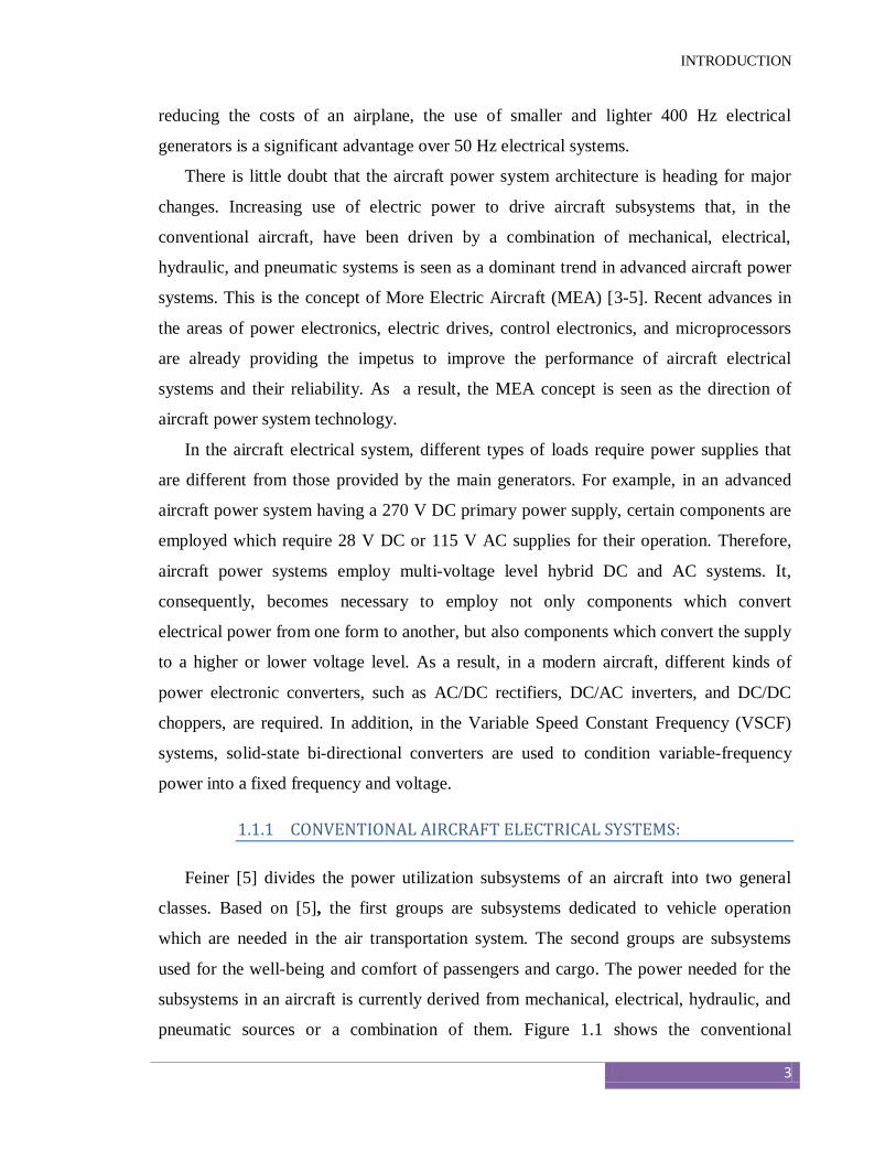
Feiner [5] divides the power utilization subsystems of an aircraft into two general
classes. Based on [5], the first groups are subsystems dedicated to vehicle operation
which are needed in the air transportation system. The second groups are subsystems
used for the well-being and comfort of passengers and cargo. The power needed for the
subsystems in an aircraft is currently derived from mechanical, electrical, hydraulic, and
pneumatic sources or a combination of them. Figure 1.1 shows the conventional

INTRODUCTION
4
subsystems driven from electrical sources. This distribution network is a point-to-point
topology in which all electrical wiring are distributed from the main bus to different loads
through relays and switches. This kind of distribution network leads to expensive,
complicated, and heavy wiring circuits.
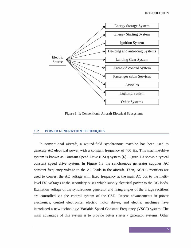
1.1.2 FUTURE ELECTRICAL LOADS
There is a trend in MEA toward replacement of more engine-driven mechanical,
hydraulic, and pneumatic loads with electrical loads due to performance and reliability
issues. Some loads considered are: flight control systems; electric anti-icing;
environmental systems; electric actuated brakes; electromechanical valve control; air-
conditioning systems; utility actuators; fuel pumping; and weapon systems. In fact,
electrical subsystems may require lower engine power with higher efficiency. Also, they
can be used only as needed. Therefore, MEA can have better fuel economy and
performance. Figure 1.2 shows the main electrical power subsystems in the MEA power
systems. Most of the electric loads require power electronic controls. In aircraft power
systems, power electronics is used to perform three different tasks. The first task is
simple on/off switching of loads which is performed by mechanical switches and relays
in conventional aircraft. The second task is the control of electric machines. The third is
not only changing the system voltage to a higher or lower level, but also converting
electrical power from one form to another using DC/DC, DC/AC, and AC/DC converters.
Similar to power electronic converters, motor drives are essential elements of the MEA.
INTRODUCTION
5
Energy Storage System
Energy Starting System
Ignition System
De-icing and anti-icing Systems
Landing Gear System
Anti-skid control System
Passenger cabin Services
Avionics
Lighting System
Other Systems
Electric
Source
Figure 1. 1: Conventional Aircraft Electrical Subsystems
1.2 POWER GENERATION TECHNIQUES
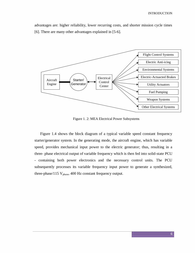
In conventional aircraft, a wound-field synchronous machine has been used to
generate AC electrical power with a constant frequency of 400 Hz. This machine/drive
system is known as Constant Speed Drive (CSD) system [6]. Figure 1.3 shows a typical
constant speed drive system. In Figure 1.3 the synchronous generator supplies AC
constant frequency voltage to the AC loads in the aircraft. Then, AC/DC rectifiers are
used to convert the AC voltage with fixed frequency at the main AC bus to the multi-
level DC voltages at the secondary buses which supply electrical power to the DC loads.
Excitation voltage of the synchronous generator and firing angles of the bridge rectifiers
are controlled via the control system of the CSD. Recent advancements in power
electronics, control electronics, electric motor drives, and electric machines have
introduced a new technology: Variable Speed Constant Frequency (VSCF) system. The
main advantage of this system is to provide better starter / generator systems. Other
INTRODUCTION
6
advantages are: higher reliability, lower recurring costs, and shorter mission cycle times
[6]. There are many other advantages explained in [5-6].
Figure 1. 2: MEA Electrical Power Subsystems
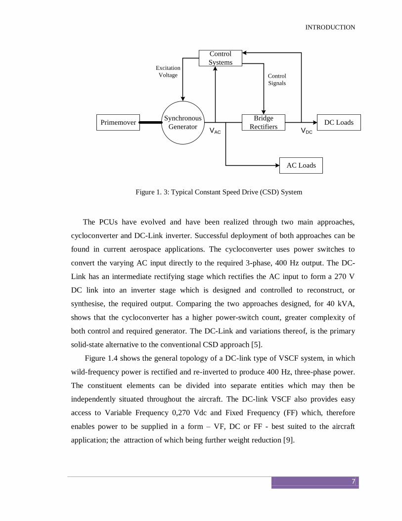
Figure 1.4 shows the block diagram of a typical variable speed constant frequency
starter/generator system. In the generating mode, the aircraft engine, which has variable
speed, provides mechanical input power to the electric generator; thus, resulting in a
three- phase electrical output of variable frequency which is then fed into solid-state PCU
- containing both power electronics and the necessary control units. The PCU
subsequently processes its variable frequency input power to generate a synthesized,
three-phase/115 Vphase, 400 Hz constant frequency output.
Flight Control Systems
Electric Anti-icing
Environmental Systems
Electric-Actuacted Brakes
Utility Actuators
Fuel Pumping
Weapon Systems
Other Electrical Systems
Electrical
Control
Center
Starter/
Generator
Aircraft
Engine
INTRODUCTION
7
Figure 1. 3: Typical Constant Speed Drive (CSD) System
The PCUs have evolved and have been realized through two main approaches,
cycloconverter and DC-Link inverter. Successful deployment of both approaches can be
found in current aerospace applications. The cycloconverter uses power switches to
convert the varying AC input directly to the required 3-phase, 400 Hz output. The DC-
Link has an intermediate rectifying stage which rectifies the AC input to form a 270 V
DC link into an inverter stage which is designed and controlled to reconstruct, or
synthesise, the required output. Comparing the two approaches designed, for 40 kVA,
shows that the cycloconverter has a higher power-switch count, greater complexity of
both control and required generator. The DC-Link and variations thereof, is the primary
solid-state alternative to the conventional CSD approach [5].
Figure 1.4 shows the general topology of a DC-link type of VSCF system, in which
wild-frequency power is rectified and re-inverted to produce 400 Hz, three-phase power.
The constituent elements can be divided into separate entities which may then be
independently situated throughout the aircraft. The DC-link VSCF also provides easy
access to Variable Frequency 0,270 Vdc and Fixed Frequency (FF) which, therefore
enables power to be supplied in a form – VF, DC or FF - best suited to the aircraft
application; the attraction of which being further weight reduction [9].
PrimemoverSynchronous
Generator
AC Loads
Bridge
RectifiersDC Loads
Control
SystemsExcitation
Voltage Control
Signals
VDCVAC

INTRODUCTION
8
As appreciated by looking at Figure 1.4 the success and optimized utilization of the
VSCF are ultimately rendered dependent on the topology, control, and located
environment of the inverter.
Figure 1. 4: Variable Speed Constant Frequency System- DC-Link Type
1.3 INVERTER TOPOLOGY
The DC/AC converters (inverters) are widely employed in many applications, such as
motor drives, active- filters and Uninterrupted Power Supply (UPS), since they are able
to supply alternate voltages with adequate magnitude and frequency to such applications.
One of the most problems associated to the inverters is the presence of an inherent
harmonic distortion of the output voltage. The THD of the resultant voltage, depending
on the used modulation, can be prohibitive in some cases. Nowadays there are several
PWM techniques [10-16] to the inverter circuits, which make possible to obtain good
output voltage by low order harmonic elimination.
The PWM techniques, to reduce sonorous pollution and size of the transformer and
output filter elements, need high switching frequency (up to 20 kHz). In high switching
frequency, the commutation losses are high and they can be greater than conduction
losses, resulting low efficiency.
Aircraft
Engine
Starter/
Generator
Rectifiers
&
Filters
Loads
Control Unit
Power Conditioning Unit
VDCVAC
Inverter FiltersVAC
INTRODUCTION
9
This section reviews the technological issues pertinent to absolutely fundamental
areas of inverter design, i.e. choice of circuit topology. In particular, the circuit can be
either “hard-switched” or “soft-switched”.
1.3.1 CONVENTIONAL INVERTER (PWM INVERTER)
“Conventional” refers in particular to the D.C. Voltage-Source-Inverter (VSI), where
the inverter (DC to AC converter) is supplied by a fixed DC voltage and its primary
power switches are subjected to hard- or stressed-switching; i.e., they have to support
rated voltage and current simultaneously during the switching transient periods - hence,
otherwise known as the Hard-Switched-Inverter (HSI). Both the synthesized AC output
voltage and frequency are controlled by using pulse-width modulated (PWM) techniques.
However, inverter has its inherent limitations of high switching losses because of
hard switching. This puts a constraint on the maximum switching frequency. It also
requires a large dc link filter and hence its time response is sluggish. For proper current
tracking, the approximate current bandwidth is usually the PWM frequency divided by a
factor of ten. Therefore, PWM based inverter fails to track high frequency components,
particularly at high power level. This is a difficult task given the current state of the art of
power semiconductor device technology [17]. Therefore current regulator limitations add
to the above mentioned problems. Additionally, the response time should be fast. Using
conventional switching techniques, inverters of over 10 kW are restricted to operate at
frequencies of below 10 kHz [18]. If the switching frequency could be raised, important
gains can be made in the areas of response time, frequency spectrum, audible noise and
modular size. The limitations of PWM inverter based systems are summarized below.
The major appeal of the conventional VSI is its simple power structure, minimal number
of power switching devices, and very high resolution pulse width control. However,
shortcomings are recognized and summarized - avoiding absolute figures - as follows:
High dV/dt, common in "hard" or "stressed" switching schemes, on the output
generates interference due to capacitive coupling and inherently high di/dt can
often display electromagnetic interference (EMI). This presents a source of
concern over compliance of the respective conducted and radiated interference to

INTRODUCTION
10
Electromagnetic Compatibility (EMC) regulations. Note, snubbing systems are
generally deployed to alleviate these problems.
Shoot-through problems (reliability), simultaneous switch on of both devices in a
phase-leg - caused by either: high dv/dt over collector-gate capacitance, inducing
charging of the input capacitor beyond the device turn-on threshold: or incorrect
gate-drive control, i.e. insufficient blanking-time between switching off one
device and turning on of the other.
Significant switching power losses, resulting in inverters with efficiencies as low
as 87% [19], and, furthermore, increased thermal management issues.
High device switching stresses. Reliability is consequently compromised and
large SOA specifications are required. High device stresses may result due to
recovery of feedback diodes.
Limitations of the maximum switching frequency. This is because switching
losses in the devices are directly proportional to the switching frequency.
Poor fault recovery characteristics
Acoustic noise is generated because switching frequency lies in the audible range
Reduced reliability due to higher heat sink temperature
1.3.2 ADVANCED, SOFT-SWITCHING INVERTERS
The "advanced" means of achieving soft-switching - where either the voltage over or
the current through the power switching devices is clamped low or to zero during the
switching transient periods - refers to use of resonant techniques. Resonant-switching
Schemes, of which there are many [17-36], are all capable, at least in principle, of
reducing the switching losses significantly. The perceived key, generic benefits over the
conventional hard-switching may be summarized as follows
Lower switching losses
Better spectral performance
Improved device utilization
Shoot-through problems due to high dv/dt are reduced
The need for snubbers disappears

INTRODUCTION
11
Device SOA is not a limiting factor
Lower sensitivity to system and packaging parasitic
The "down side" to realizing these benefits is that other factors such as additional
stress on the components, component count and size, conduction losses, and control
complexity may render the practical realization unsuitable for the intended application.
There are various ways of classifying these inverters [24-25]; mostly into two
families - Resonant Link Inverters (RLI) and Pole Commutated Inverters (PCI).
1.3.2.1 Pole Commutated Inverters (PCI)
PCIs are characterized by a resonant commutation circuit per pole of the inverter. In
its raw form - no auxiliary circuit aiding the commutation process - the PCI suffers from
peak current stresses in its switching devices and poor dc bus voltage utilization. Most
variants of the PCI use additional components to ease these failings, the most successful
of which appears to be the Auxiliary Resonant Commutated Pole (ARCP) inverter
associated with R. W. DeDoncker [34], see Figure 1.5.
Inverter
Loads
Vdc
Rectifier
FilterGenerator
Commutative
CircuitVdc/2
Lr
Vdc/2
Cr/2
Cr/2
VX
Figure 1. 5: The Auxiliary Resonant Commutated Pole (ARCP)
The basic objective is to, swing, or resonate, Vx (centre of the totem-pole) from one
supply rail to the other, at which point the opposite switch, with its parallel free-wheel
diode conducting, can be turned-on under ZVS conditions. Each primary switch is also
paralleled by a substantial snubber/resonant capacitor (Cr/2) which forces highly snubbed
(near ZVS) turn-off conditions. These capacitors can be large in value because the

INTRODUCTION
12
resonant impedance which they form along with the auxiliary resonant inductor (Lr) has
no effect on the device current rating.
If not enough energy exists to enable losses to be overcome during the voltage swing
and, therefore, for the supply rails to be reached, the "on" going device must absorb
losses due to the non-ZVS condition - including the energy dumped from its parallel
capacitor which has not been fully discharged. Thus there are conditions where the
energy made available for swinging Vx needs to be boosted in order to ensure the
clamping action of the opposite main free-wheel diode to the supply; i.e., a ZVS turn-on
opportunity. Hence the introduction of the auxiliary circuit (2xdiode, 2xswitch, MCTs or
Thyristors..., and Lr) parallel to the pole. This circuit is operated under ZCS conditions
and although the peak current stress in the inductor and switches can be typically 1.3-1.8
p.u., the duty cycle is very low - the rms ratings of the auxiliary circuit elements can,
therefore, be small. Furthermore, unlike the RLI, the resonant inductor of a PCI is not in
the main power-flow path, thus steering the circuit towards higher power applications.
However, the circuit incurs the penalty of component count which is clearly higher than
in the RLI.
1.3.2.2 Resonant Link Inverters (RLI)
Resonant Link inverters (RLI) are characterized by a resonant commutation circuit
placed at a point of common connection; i.e. on the dc bus side of the inverter.
The Actively Clamped Resonant DC Link Inverter
The Actively Clamped Resonant DC Link (ACRDCL) inverter [20] of Figure 1.6
represents a development on one of the earliest RLIs. Initially proposed by, Prof. Deepak
M. Divan [19]. In its original/simple form - without the active clamp circuit - the dc bus,
or link, is made to oscillate between a value greater than twice the DC supply (Vdc) and
zero volts. At which point a change of inverter switch status may be performed without
incurring switching losses; hence, ZVS. The zero volt bus instants are determined by the
resonant components (Lr and Cr) and cannot, therefore, be explicitly controlled. This
means that the a.c. output will be synthesized by an integer number of resonant pulses.
Such a Discrete Pulse Modulation (DPM) strategy may raise questions on the resolution
of output synthesis and, furthermore, can generate sub-harmonics at frequencies
INTRODUCTION
13
significantly below half the link frequency. These may, therefore, be viewed as flaws in
the RLI approach. Indeed, most variations of the RLI are attempts to offer true PWM
control and resolution over the switching instants; primarily at a cost of extra component
count aid control complexity. In addition, investigations [24] indicate that in terms of
spectral content, or Total Harmonic Distortion (THD), the ACRDCLI offers
improvements over the conventional HSI if operating at switching frequencies greater
than 13 kHz [24].
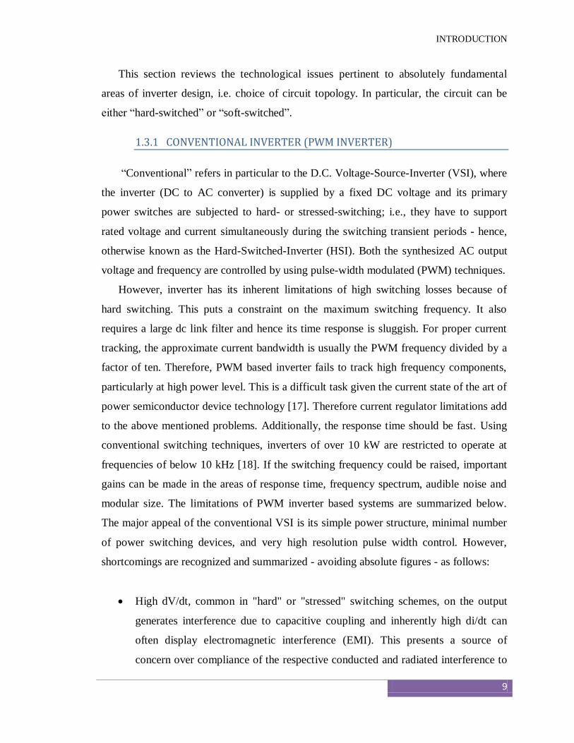
The most apparent penalty imposed by the RDCLI is the peak voltage stress due to dc
bus oscillations greater than twice Vdc. This can be alleviated by the introduction of an
active clamp which will divert energy away from the inverter during peak bus voltage
periods and return it in order to collapse the bus voltage to zero, thus limiting, or
"clamping," the bus voltage to 1.3 1.8 x Vdc.
Figure 1. 6: The Actively Clamped Resonant Dc Link (ACRDCL)
Resonant DC Link Inverters
Resonant dc link inverters promise marked gains for adjustable speed drives, power
supplies and active filtering applications. Among the various types of resonant links, the
parallel resonant DC link is quite attractive for implementing zero voltage switching
(ZVS) [19]. This is based on shunt resonance. This inverter is quite simple in the sense
that it needs a minimum number of devices, it is easy to implement and requires simple
control. Compared to a regular pulse width modulated (PWM) inverter this inverter
InverterCr
Resonant Commutative Circuit
Sm
Dm
Loads
Vdc
Rectifier
FilterGenerator
Dc
Active Clamp
Cc
Lr
Sc
INTRODUCTION
14
requires an additional resonant inductor and a resonant capacitor. The resonant circuit is
connected between dc source and the inverter so that the input voltage to the inverter
oscillates between zero and to a value that is slightly greater than twice the dc bus
voltage. The advantage of this soft-switched inverter is well known [19-20], [35-36]. It
reduces the dominant switching losses in the inverter devices, allows higher switching
frequencies at reasonably high power level and reduces noise and electromagnetic
interference. Because of the minimal switching loss, the efficiency is high and cooling
requirement is minimal. Additionally, the devices do not require any snubbers.
This simple topology however has few drawbacks. These are higher device
voltage stresses (when the output voltage is greater than twice the dc input voltage), zero
crossing failure unless the initial current in the resonant inductor is built properly. The
voltage overshoot problem can be overcome by using actively clamped RDCLI [20].
Through clamping it is possible to limit the voltage stresses of the inverter devices to 1.3
to 1.8 times the dc voltage. The actively clamped RDCLI circuit however has few
disadvantages. The link frequency varies with variation in the dc link voltage. This
manifests itself in large current jumps. This topology increases losses due to introduction
of the clamping circuit. The additional clamping device increases the complexity of the
power circuit and the control circuit. Moreover, the control of the clamping device
becomes extremely difficult at high frequencies [37].
In this thesis the basic RDCLI is considered for power circuit of the inverter. An
important consideration for successful operation of RDCLI is that there should not be any
zero crossing failure. Zero crossing of the resonant link DC voltage is mandatory in every
resonant cycle for successful operation of the inverter. Failure of resonant link tends to
occur because of the finite Q of the resonant circuit where the capacitor voltage tends to
build up in successive resonant cycles. Therefore an appropriate initial current must be
built up in the inverter which would then ensure a zero crossing of the voltage. This must
be done in every resonant cycle. The built up of fixed initial inductor current is adopted
to ensure zero crossing in every resonant cycle in [19]. However, the initial current is a
function of the inverter input current, which depends upon the load current of the
inverter. In a practical circuit, the load current would fluctuate and hence the load current
seen by the resonant link can be bi-directional. Thus using a fixed initial inductor current

INTRODUCTION
15
concept would not ensure zero crossing in every resonant cycle unless this current is
designed on the worst case basis. This approach however would aggravate the voltage
overshoot problem. A programmable initial current control technique for RDCLI was
reported in [34-36]. This scheme is somewhat complex from the implementation
viewpoint. A current prediction scheme is proposed in [37] for finding out the initial
current. The functioning of the link depends on the detection of the zero crossing of the
resonant capacitor. This scheme requires a sensitive detection of zero voltage crossing.
In this thesis we present a new current initialization technique [27, 38] for the
resonant circuit which ensures reliable zero voltage switching. The proposed method is
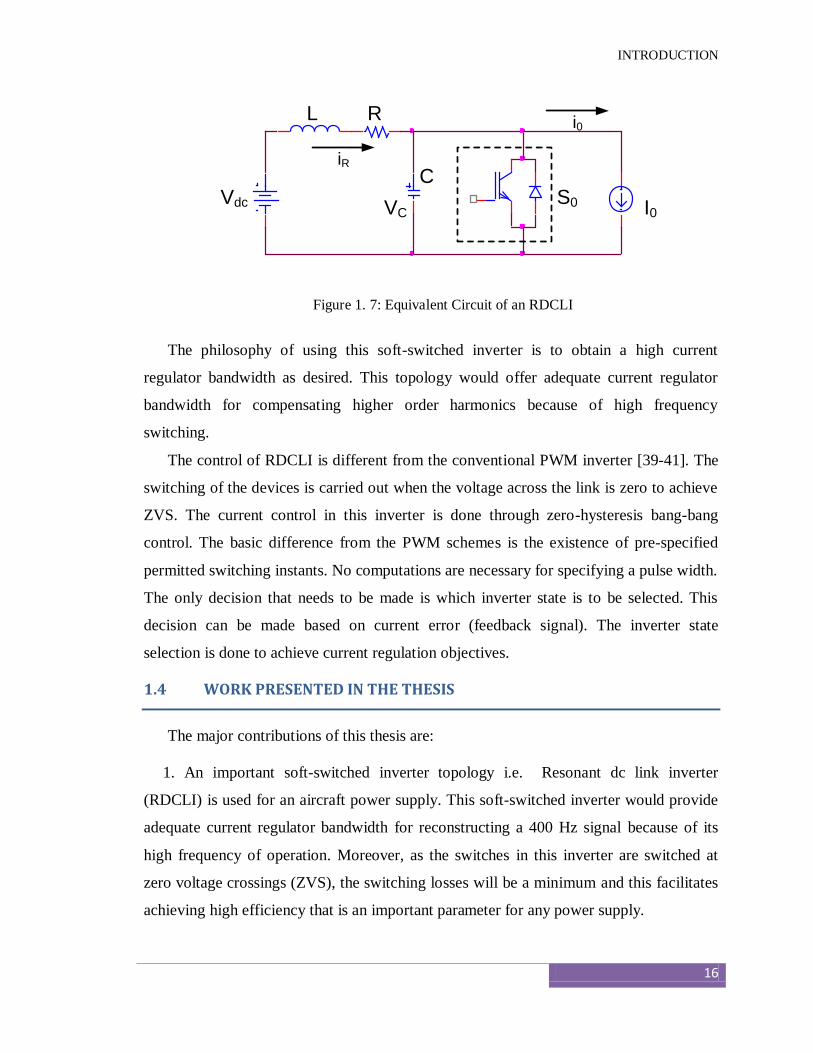
based on state transition equation and is simple to implement. The equivalent circuit of a
RDCLI is shown in Figure 1.7. This contains a resonant circuit generated by an inductor
(L) and a capacitor (C) as shown in this figure. The inductor coil has a resistance (R) due
to its finite Q-factor. The voltage (Vc) across the capacitor is called the dc link voltage.
Using the resonant circuit properties, this voltage goes through zero periodically. The
switch (S0) as shown in Figure 1.7 represents the switch across the link. This switch is
required to short the link when the voltage Vc is zero for the current iR to build up. The
current i0 is the input current of the inverter, this act as the load current for the resonant
link. It is assumed that the current i0 remains constant during a resonant oscillation
period. Therefore this current is indicated by the current source I0.
The philosophy is to switch the device only when the voltage across it is zero. For
a given set of resonant link parameters, a constant resonant oscillation period is selected.
The state vector consists of link capacitor voltage (Vc) and inductor current (iR) in Figure
1.7. The capacitor voltage must be zero at the start and at the end of every resonant
oscillation period for successful ZVS. With this condition, the exact initial value of the
inductor current (iR) is determined. In order to start a resonant cycle with this value of the
initial current, the time duration for which the dc bus must be shorted can be calculated.
Thus, the initial inductor current is generated by shorting the link and a resonant cycle
commences with proper values of capacitor voltage (zero) and inductor current. This
forces the link capacitor voltage to return to zero after a pre-specified resonant oscillation
period.
INTRODUCTION
16
Figure 1. 7: Equivalent Circuit of an RDCLI
The philosophy of using this soft-switched inverter is to obtain a high current
regulator bandwidth as desired. This topology would offer adequate current regulator
bandwidth for compensating higher order harmonics because of high frequency
switching.
The control of RDCLI is different from the conventional PWM inverter [39-41]. The
switching of the devices is carried out when the voltage across the link is zero to achieve
ZVS. The current control in this inverter is done through zero-hysteresis bang-bang
control. The basic difference from the PWM schemes is the existence of pre-specified
permitted switching instants. No computations are necessary for specifying a pulse width.
The only decision that needs to be made is which inverter state is to be selected. This
decision can be made based on current error (feedback signal). The inverter state
selection is done to achieve current regulation objectives.
1.4 WORK PRESENTED IN THE THESIS
The major contributions of this thesis are:
1. An important soft-switched inverter topology i.e. Resonant dc link inverter
(RDCLI) is used for an aircraft power supply. This soft-switched inverter would provide
adequate current regulator bandwidth for reconstructing a 400 Hz signal because of its
high frequency of operation. Moreover, as the switches in this inverter are switched at
zero voltage crossings (ZVS), the switching losses will be a minimum and this facilitates
achieving high efficiency that is an important parameter for any power supply.
L R
S0
C
VCVdc
iR
i0
I0

INTRODUCTION
17
2. In this thesis a new algorithm for current initialization scheme is proposed for the
resonant dc link inverter (RDCLI). The method of current initialization is based on the
state transition analysis of the system as a boundary value problem (BVP). This technique
makes it possible to operate the resonant dc link inverter without any zero-crossing
failure, which is an important issue for a satisfactory operation of such an inverter. A
zero-hysteresis bang-bang control is used for current control of the inverter. Switchings
in this case can only be done when the link voltage is zero. Just before the zero voltage
condition occurs, generated reference currents are compared with their corresponding
actual values to generate these error signals. Depending on the polarity of these signals a
switching decision is taken. Since there is no notion of hysteresis band in this case, we
will call this as zero-hysteresis bang-bang current control.
3. Detailed analysis of the losses in the resonant DC link inverter is performed.
Equations for estimating the various losses in the resonant DC link inverter and an
equivalent hard switching inverter are developed. Based on these equations, a design
optimization is performed for the resonant DC link inverter to find the optimum values of
the link components. Finally, a comparison of the losses in the resonant inverter and hard
switched inverter is made.
4. Development of prototypes for power supply and the associated control circuits,
namely for (i) ZVS (State Transition equation based Zero Voltage Switching Control)
and current initialization (Zero Hysteresis Bang-Bang current control).
5. PC interface is used for the implementation of the proposed current initialization
scheme. The use of a PC makes the system more flexible for conducting experiments.
This facilitates zero-voltage switching by taking into account of the actual circuit delays
and tolerances. Furthermore, PC is replaced by FPGA, which reduces controller circuit
size also expands scope for developing an application specific integrated circuit (ASIC).
1.5 THESIS LAYOUT
Chapter 2: It describes the operating principles of the resonant DC link inverter. A
new algorithm for current initialization scheme is proposed that ensures ZVS. The current
control within the inverter is done through zero-hysteresis bang-bang control. The
inverter switching state selection is done to achieve regulation objectives. It also presents

INTRODUCTION
18
a simulation study of the resonant DC link inverter feeding an RL load at 400 Hz thus
validating the concept of an aircraft power supply.
Chapter 3: Here power losses in the resonant DC link inverter are estimated, and the
optimal values of resonant components are determined. It also details the design of a
resonant link control circuit.
Chapter 4: The components and construction of a prototype resonant DC link
inverter are described. Details of the power circuits, various control circuits and PC
interface are presented. The use of PC for the current initialization makes the circuit
simpler and flexible.
Chapter 5: We present the experimental results obtained in the laboratory through
lab prototypes. The experimental results are in close agreement with the theoretical
results thus validating the concepts presented in this thesis. Finally PC is being replaced
by FPGA which performs the proposed algorithm (i.e., generating the Reference for
successful operation of Zero voltage switching).
Chapter 6: The general conclusions derived from this thesis are presented. This
chapter also presents some future directions for research in this area.
19
CONTROL CIRCUIT FOR
AIRCRAFT POWER SUPPLY
USING SOFT-SWITCHED
INVERTER
HIS chapter describes the design of a novel aircraft power supply.
Power supply design is designed using a soft-switched Resonant DC Link
Inverter (RDCLI). A current initialization scheme based on state transition
equation is adopted to avoid zero crossing failures. Zero-hysteresis bang-bang control
is used for current control within the inverter. The designed power supply supports
load of 400 Hz. The advantages of the power supply design using soft-switched
inverter rather than conventional hard switched PWM inverter in terms of adequate
current regulator bandwidth and reduced switching losses are brought out. The
proposed solution is validated through extensive MATLAB and CASPOC simulation.
T
Chapter
2
CONTROL CIRCUIT FOR AIRCRAFT POWER SUPPLY USING SOFT-SWITCHED
INVERTER
20
2.1 INTRODUCTION
The conventional voltage source inverter for motor drive encountered severe
problems such as high Electromagnetic interference (EMI), wide range of harmonics,
heavy acoustic noise and low efficiency. Resonant DC-link inverter technique
becomes dominate in solving the above problems due to its simplicity in both power
stage topology and control strategy. A new 400 Hz aircraft power generating system
is introduced which has been designed to achieve significant improvements in power
density and reliability compared with conventional systems now in use. At the heart
of the new variable – speed constant frequency (VSCF) Resonant Link Inverter
designed so that all inverter switching losses and significant reductions in power
device switching stresses and EMI generations [46, 47]. In this chapter, operation
principle of resonant DC-link inverter is analyzed
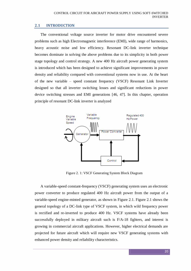
Figure 2. 1: VSCF Generating System Block Diagram
A variable-speed constant-frequency (VSCF) generating system uses an electronic
power converter to produce regulated 400 Hz aircraft power from the output of a
variable-speed engine-minted generator, as shown in Figure 2.1. Figure 2.1 shows the
general topology of a DC-link type of VSCF system, in which wild frequency power
is rectified and re-inverted to produce 400 Hz. VSCF systems have already been
successfully deployed in military aircraft such is F/A-18 fighters, and interest is
growing in commercial aircraft applications. However, higher electrical demands are
projected for future aircraft which will require new VSCF generating systems with
enhanced power density and reliability characteristics.

CONTROL CIRCUIT FOR AIRCRAFT POWER SUPPLY USING SOFT-SWITCHED
INVERTER
21
In the VSCF, the generator input is coupled directly to the raw, variable source
speed of the engine drive-shaft; thus, resulting in a electrical output of variable
frequency which is then fed into solid state PCU - containing both power electronics
and the necessary control units [Figure 1.4]. The PCU subsequently processes its
variable frequency input power to generate a synthesized, 400 Hz constant frequency
output.
2.2 Resonant DC Link Inverter Topology
In soft-switched Inverter either the voltage across or the current through the power
switching devices is clamped low or to zero during switching transient periods –
refers to the use of resonant techniques. Resonant switching schemes of which there
are many [17-36], [42-45] are all capable, at least in principle, of reducing the
switching losses significantly. The perceived key, generic benefits over the
conventional hard-switching may be summarized as follows:
Lower switching losses
dv/dt reduction
The need for snubbers disappears
Device SOA is not a limiting factor
Better spectral performance
Improved device utilization
Lower sensitivity to system and packaging parasitic.
The RDCLI was proposed by Divan [19]. This soft-switched inverter is suitable
for high power applications (Upto 500 KVA). It also requires a minimum number of
devices, easy to implement and requires simple control. The schematic diagram of a
single-phase parallel resonant dc link inverter that runs from a dc supply (Vdc) is
shown in Figure 2.2. It requires an additional inductor and a capacitor compared to a
regular pulse width modulated (PWM) inverter. This inductor-capacitor pair forms the
resonant circuit. The resonant circuit is connected between the dc source and the
inverter so that the input voltage to the inverter oscillates between zero and slightly
greater than twice the dc bus voltage.
Figure 2.3 shows an approximate equivalent circuit of the RDCLI. Here the
resistance R in series with the inductance L represents the resistance of the inductor

CONTROL CIRCUIT FOR AIRCRAFT POWER SUPPLY USING SOFT-SWITCHED
INVERTER
22
due to its finite Q-factor. It is assumed that the current i0 remains constant during a
resonant oscillation period. Therefore this current is indicated by the current source I0.
The voltage (Vc) across the capacitor is called the dc link voltage. Using the resonant
circuit properties, this voltage goes through zero periodically. The four switches that
are connected across the link are switched when the link voltage is zero. The switch
(S0) as shown in Figure 2.3 represents the switch across the link. This switch is
required to short the link for the current iR to build up. The same can be also achieved
by shorting the two switches of the inverter in the any leg.
Figure 2. 2: Circuit Schematic of a Single Phase RDCLI
Figure 2. 3: Equivalent Circuit of a RDCLI
This simple topology however has few drawbacks — Higher device voltage
stresses (especially when the output voltage is greater than twice the dc input voltage)
and zero crossing failure unless the initial current in the resonant inductor is built up
Rs
C
L
S0
S3
S2
S1
S4
R
VdcVc
+
To Load
Rs
C
L
S0
R
VdcVc
+
iR
I0
i0
CONTROL CIRCUIT FOR AIRCRAFT POWER SUPPLY USING SOFT-SWITCHED
INVERTER
23
properly. The voltage overshoot problem can be overcome by using actively clamped
RDCLI [20]. It is possible to limit the voltage stresses of the inverter devices to 1.3 to
1.8 times the dc voltage. However, actively clamped RDCLI circuit has few
disadvantages [20]. The link frequency varies with variation in the dc link voltage.
This shows large current jumps. Furthermore, this topology increases losses due to
introduction of the clamping circuit. The additional clamping device increases the
complexity of the power and control circuits. Moreover the control of the clamping
device becomes extremely difficult at high frequencies [37]. Therefore, active
clamping is not considered in this thesis.
An important consideration for successful operation of RDCLI is that there should
not be zero crossing failures, as link voltage (i.e., voltage across the capacitor C) must
go to zero at the end of every resonant cycle for zero voltage switching. This is easily
achieved if the resonant inductor L has infinite Q factor. In such a case the circuit will
oscillate between zero and 2Vdc with a frequency of CL21 Hz. However, in
practice an inductor with infinite Q cannot be obtained. Even high quality inductors
will have a Q factor around 150 to 200. It is thus important to devise a mechanism
through which the dc link voltage is forced to zero at the end of every resonant cycle.
This is achieved through the shorting switch.S0. This switch is shorted for a finite
duration of time at the end of each resonant cycle to build up the current iR to a level
such that it can overcome the loss (I2R loss) of the inductor. This will ensure that the
voltage will build up to 2Vdc before becoming zero at the end of the resonant cycle.
This building up of the current to a desired value is called current initialization. It
is also to be noted that the inverter switches (S1 – S4) are operated through a desired
modulation technique only during the interval when the link voltage is maintained
zero, i.e., when the shorting switch S0 is closed. The building up of fixed initial
inductor current was first proposed in [19]. However, the initial current is a function
of the inverter load current i0. In a practical circuit, the load current would fluctuate
and can also be bi-directional. Thus using a fixed initial inductor current concept
would not ensure zero crossing in every resonant cycle unless this current is designed
on the worst case basis. Furthermore, this approach would aggravate the voltage
overshoot problem. A programmable initial current control technique for an RDCLI
was reported in [35]. This scheme is somewhat complex from the implementation
viewpoint. In this thesis we present a novel current initialization technique for the
CONTROL CIRCUIT FOR AIRCRAFT POWER SUPPLY USING SOFT-SWITCHED
INVERTER
24
resonant circuit which ensures reliable zero voltage switching. The proposed method
is based on state transition equation and is simple to implement.
2.3 CURRENT INTIALIZATION SCHEME
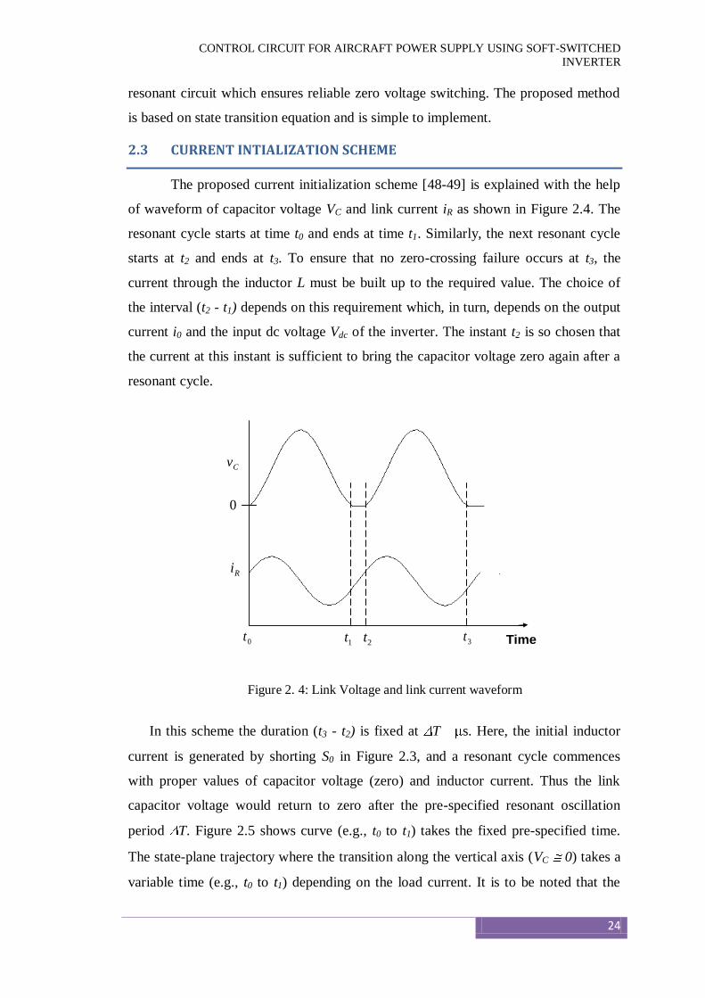
The proposed current initialization scheme [48-49] is explained with the help
of waveform of capacitor voltage VC and link current iR as shown in Figure 2.4. The
resonant cycle starts at time t0 and ends at time t1. Similarly, the next resonant cycle
starts at t2 and ends at t3. To ensure that no zero-crossing failure occurs at t3, the
current through the inductor L must be built up to the required value. The choice of
the interval (t2 - t1) depends on this requirement which, in turn, depends on the output
current i0 and the input dc voltage Vdc of the inverter. The instant t2 is so chosen that
the current at this instant is sufficient to bring the capacitor voltage zero again after a
resonant cycle.
Figure 2. 4: Link Voltage and link current waveform
In this scheme the duration (t3 - t2) is fixed at T s. Here, the initial inductor
current is generated by shorting S0 in Figure 2.3, and a resonant cycle commences
with proper values of capacitor voltage (zero) and inductor current. Thus the link
capacitor voltage would return to zero after the pre-specified resonant oscillation
period T. Figure 2.5 shows curve (e.g., t0 to t1) takes the fixed pre-specified time.
The state-plane trajectory where the transition along the vertical axis (VC 0) takes a
variable time (e.g., t0 to t1) depending on the load current. It is to be noted that the
Time 3t 2t 1t 0t
0
Cv
Ri

CONTROL CIRCUIT FOR AIRCRAFT POWER SUPPLY USING SOFT-SWITCHED
INVERTER
25
particular value of T chosen depends on the parameters of the resonant circuit. Since
a resonant cycle time is much smaller than the time constant of the load circuit, the
load current is assumed to be a constant current equal to I0 over a particular resonant
cycle, i.e., between T = t3 - t2.
Referring to Figure 2.3, let us define a state vector as T
Rc ivx and an input
vector asT
dcVIu 0 . The state space equation of the circuit is then given by
x Ax Bu (2.1)
Where the matrices A and B are given by
AC
L R LB
C
L
0 1
1
1 0
0 1,
The solution of (2.1) at instant t3 based on the initial condition at instant t2 is given
by
( )
3 20
( ) ( ) ( )T
A T A Tx t e x t e Bu d (2.2)
It is to be noted that in the above equation Vdc is constant and I0 is assumed to be
known and constant. Also noting that capacitor voltage must be equal to zero at
instant t3, defining a row vector C as C 1 0 , we can write from (2.2)
0 2 2C x t u t( ) ( )
(2.3)
Where eA T and e BdA T
T( )
0
Note that since A, B and T are known a priori, the matrices and can be
numerically evaluated. The state plane trajectory under this boundary value problem

CONTROL CIRCUIT FOR AIRCRAFT POWER SUPPLY USING SOFT-SWITCHED
INVERTER
26
is shown Figure 2.5 where VC is assumed to be approximately zero when S0 is closed.
We can expand equation (3) as
)()(0 2121121211 tutx
Figure 2. 5: State Plane Diagram of link voltage and current
Where the subscripts 11 and 12 indicate the particular elements of these matrices.
Again from Figure 2.4 we get .)(0)( 22 titx R
T. Substituting in the above equation
and rearranging we get
0
11 12 11 12
2
12 2 11 0 12
00 * *
( )
* ( ) [ * * ]
R dc
R dc
I
i t V
i t I V
dcR VIti 12011
12
2
1)( (2.4)
The above value of current at instant t2 required to ensure zero crossing of the
voltage at instant t3. Once iR(t2) is obtained the time for which the capacitor should be
shorted. The computed value of current iR(t2), obtained from equation (2.4), with the
actual value link current iR. The switch S0 is opened when these two values are equal.
This ensures that the link current is built up to the required level of initial current such
that the link voltage goes to zero at instant t3, i.e., at the end of next resonant cycle.
With the value of inductor, 33 H and the value of capacitor, 1 F, the un-damped
oscillation time is 35.72 s. It is seen from the simulation studies that the t2 – t1 is
coming around 3 to 5 s, which is sufficient time to build the link current for
onturned
,,
0
31
S
ttt
offturned
,,
0
20
S
ttt
0 Cv
Ri
CONTROL CIRCUIT FOR AIRCRAFT POWER SUPPLY USING SOFT-SWITCHED
INVERTER
27
successful operation of ZVS. With these values of inductor and capacitor the un-
damped oscillation time is 35.72 s. Therefore, the resonant cycle time T is chosen
to be 30.72 s taking into account the finite Q-factor of the coil.
2.4 Effect of Link Frequency Variation on Output Current
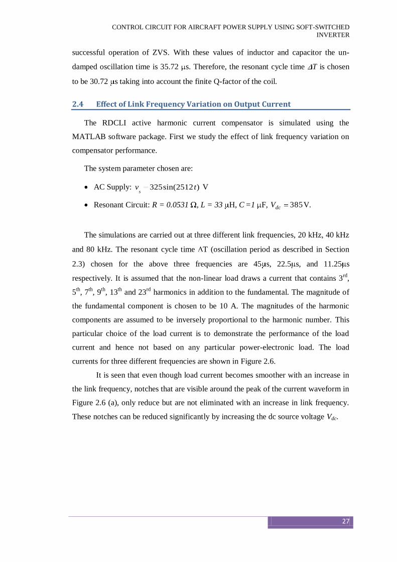
The RDCLI active harmonic current compensator is simulated using the
MATLAB software package. First we study the effect of link frequency variation on
compensator performance.
The system parameter chosen are:
AC Supply: 325sin(2512 )s
v t V
Resonant Circuit: R = 0.0531 , L = 33 H, C =1 F, 385dcV V.
The simulations are carried out at three different link frequencies, 20 kHz, 40 kHz
and 80 kHz. The resonant cycle time T (oscillation period as described in Section
2.3) chosen for the above three frequencies are 45 s, 22.5 s, and 11.25 s
respectively. It is assumed that the non-linear load draws a current that contains 3rd
,
5th, 7
th, 9
th, 13
th and 23
rd harmonics in addition to the fundamental. The magnitude of
the fundamental component is chosen to be 10 A. The magnitudes of the harmonic
components are assumed to be inversely proportional to the harmonic number. This
particular choice of the load current is to demonstrate the performance of the load
current and hence not based on any particular power-electronic load. The load
currents for three different frequencies are shown in Figure 2.6.
It is seen that even though load current becomes smoother with an increase in
the link frequency, notches that are visible around the peak of the current waveform in
Figure 2.6 (a), only reduce but are not eliminated with an increase in link frequency.
These notches can be reduced significantly by increasing the dc source voltage Vdc.
CONTROL CIRCUIT FOR AIRCRAFT POWER SUPPLY USING SOFT-SWITCHED
INVERTER
28
0 0.5 1 1.5 2 2.5 3 3.5 4 4.5 5
x 10-3
-10
-5
0
5
10
Time(s)
Curr
ent
(A)
0 0.5 1 1.5 2 2.5 3 3.5 4 4.5 5
x 10-3
-10
-5
0
5
10
Time (s)
Curr
ent
(A)
0 0.5 1 1.5 2 2.5 3 3.5 4 4.5 5
x 10-3
-10
-5
0
5
10
Time (s)
Curr
ent
(A)
Figure 2. 6: Output Load Currents at Different link Frequencies
(a) f=20 kHz, (b) f=40 kHz, (c) f=80 kHz
(a) Frequency = 20 KHz
(b) Frequency = 40 KHz
(c) Frequency = 80 KHz

CONTROL CIRCUIT FOR AIRCRAFT POWER SUPPLY USING SOFT-SWITCHED
INVERTER
29
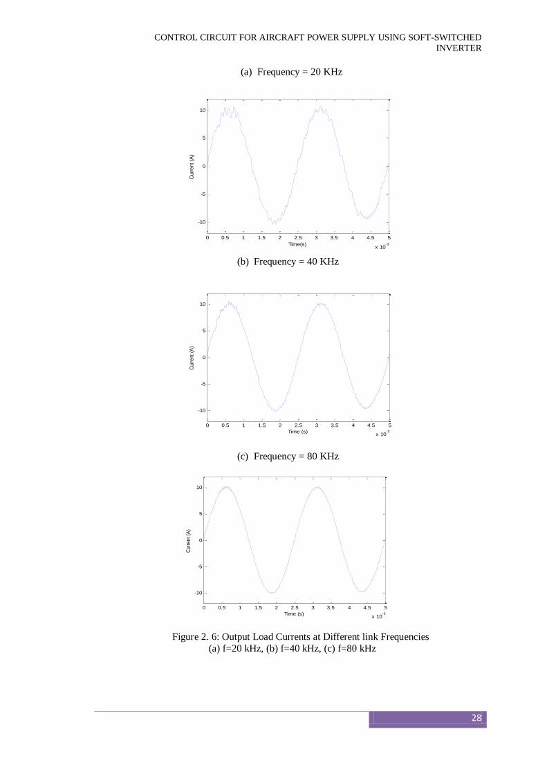
2.5 Effect of DC Source Voltage Variation on Output Current
Figure 2. 7: Output Load Currents at (a) Vdc = 385 Volts,
(b) Vdc = 435 Volts, (c) Vdc = 470 Volts
CONTROL CIRCUIT FOR AIRCRAFT POWER SUPPLY USING SOFT-SWITCHED
INVERTER
30
The load current waveform is almost sinusoidal except for some notches at the
peak of the load current. This can be explained as follows, load current coincides with
that of the reference current, the voltage difference between the inverter and the
reference voltage at load end is minimum (that is the rate of change of current,v = L *
di/dt) during the period when these notches are present. Thus to force a current
rapidly through inductor L a high dtdi is required. This can only be achieved by
increasing Vdc. Figure 2.7 shows load currents and the reference currents from the
source at three different values of dc source voltages, namely, 385 V, 435 V and 470
V.
These simulations are carried out for a link switching frequency of 20 kHz. The
notches present in Figure 2.7 disappear with an increase in the dc source voltage.
The performance and system identification of Resonant DC Link Inverter is done
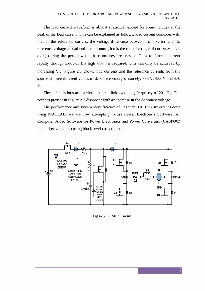
using MATLAB; we are now attempting to use Power Electronics Software i.e.,
Computer Aided Software for Power Electronics and Power Converters (CASPOC)
for further validation using block level components.
PLUS MINUS
B
1
BMK
L2
14m
Rload
0.2
G1
G1
G2
G2
ILD1 D2
D3D3
R
1
33m
L1
33e-6
IR
V1 30 D1
1m
R
E
S
R
C1=1E-6
CURRENT FROM
SENSOR IR TO
COMPARATOR
(FIG. 2.9)
TO GATE
OF IGBT
FOR ZVS
FROM
JKFF
(FIG. 2.9)
VDC FROM
VOLTAGE
SENSOR
Figure 2. 8: Main Circuit

CONTROL CIRCUIT FOR AIRCRAFT POWER SUPPLY USING SOFT-SWITCHED
INVERTER
31
BMK
GATETIME
DC
AC
F
PHASE
D
REFERENCE
SIGNAL
SIGNAL1
TIME
I(Rload)
CURRENT
O
i
SPL
G1
G2
1U Tdelay
DELAY
i
DELAY1
AND
NOR
COMP1
COMPARATOR
a
b
c
d
e
EXPRESSION
IMAX- 4.4204
4.4074
0.3749
VDC
IL
COMP2
COMPARATOR
Q
Q
CLK
CLR
J
K
PR
1
0
NOT
NOT
TIME
DC
AC
F
PHASE
D
FOR LOAD SIDETIME
0
32.6
400
0
0
CURRENT
FROM
SENSOR IR
TO GATE OF
IGBT FOR
ZVS
1
Z
Z1
Z11
TON
30.72US
0
2
400
0.5
0
Figure 2. 9: Controller Circuit
Figure 2.8 shows the main circuit of the aircraft power supply using Resonant DC
Link Inverter (RDCLI). Here the oscillatory (LC) is connected across the DC supply
whose values are L=33 H and C= 1 F. It is assumed that the inductor is not pure and
so we have included resistance into the circuit and the value to be taken is R=33 mΩ.
All the values taken are based on actual values, which are supposed to be used in
physical circuits. One Voltage sensor and two Current sensors have been used to
calculate the instant voltage and current. The Load is connected with one inductor
(L=14 mH), one Resistor (0.2 Ω) and a Back Emf of 32.6V and 400 Hz. The required
initial current is computed in the Expression Block (Figure 2.9). The computation
time required is much smaller than the resonant cycle time T.
The required initial current, which is computed in the expression block of Figure
2.9, is then available to the comparator for comparison with the actual link current.
The link current is monitored continuously through a sensor IR, Figure 2.8. When the
link current becomes equal to the required initial current, the comparator (2) output
becomes zero. The output is used for clearing the J-K flip-flop (Figure 2.9). Once this

CONTROL CIRCUIT FOR AIRCRAFT POWER SUPPLY USING SOFT-SWITCHED
INVERTER
32
flip-flop is cleared, its output (Q) becomes zero and QN becomes one. This is then
used for switching off S0. Simultaneously, the inverted output (QN) of the J-K flip-
flop is used for triggering the mono-stable (Figure 2.7) through an inverting buffer.
The mono-stable timing is designed for a pulse-width of T=30.72 s. After this time
elapses, the negative going edge of the mono-stable output is used to clock the J-K
flip-flop. This force the output of the flip-flop to one and consequently the shorting
switch S0 is turned on.
Through the above scheme, the zero-voltage switching is obtained. It is to be
noted that during the time when S0 is on, the switching transitions of the switches S1 –
S4 take place. To ensure that the switches S1 – S4 are turned on or off only during this
prescribed interval, the gating of S1 – S4 are conditioned by the output Q of the J-K
flip-flop. Further note that the configuration of the switches S1 – S4 at a particular
resonant cycle is dependent on the load connected to the output of the inverter. Zero-
voltage switching along with link current waveform is shown in Figure 2.10.
Figure 2. 10: Zero-voltage Switching and Link Current waveforms
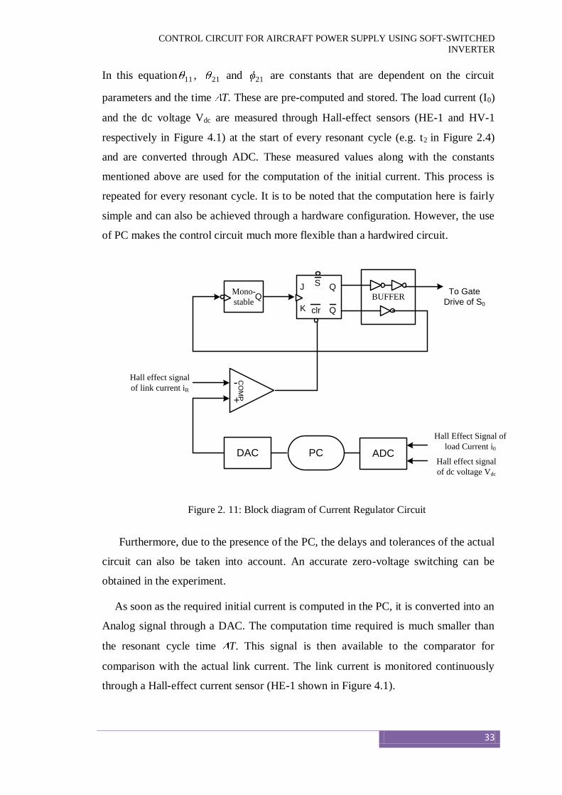
The block diagram of the proposed circuit for current initialization scheme is
presented in Figure 2.11 for further clarity. A personal computer (PC) along with its
associated high-speed analog-to-digital converter (ADC) and digital-to-analog
converter (DAC) is used for the computation of the initial current from equation (2.4).
5.000
10.000
15.000
20.000
25.000
30.000
35.000
40.000
45.000
50.000
55.000
60.000
65.000
-5.000
-10.000-10.523
68.073
391.032u 441.032u 491.032u 541.032u 591.032u 641.032u 691.032u 741.032u 791.032u 841.032u 891.032u 941.032u 991.032u 1041.032u 1091.032u 1141.032u 1191.032u
CONTROL CIRCUIT FOR AIRCRAFT POWER SUPPLY USING SOFT-SWITCHED
INVERTER
33
In this equation 11 , 21 and 21 are constants that are dependent on the circuit
parameters and the time T. These are pre-computed and stored. The load current (I0)
and the dc voltage Vdc are measured through Hall-effect sensors (HE-1 and HV-1
respectively in Figure 4.1) at the start of every resonant cycle (e.g. t2 in Figure 2.4)
and are converted through ADC. These measured values along with the constants
mentioned above are used for the computation of the initial current. This process is
repeated for every resonant cycle. It is to be noted that the computation here is fairly
simple and can also be achieved through a hardware configuration. However, the use
of PC makes the control circuit much more flexible than a hardwired circuit.
Figure 2. 11: Block diagram of Current Regulator Circuit
Furthermore, due to the presence of the PC, the delays and tolerances of the actual
circuit can also be taken into account. An accurate zero-voltage switching can be
obtained in the experiment.
As soon as the required initial current is computed in the PC, it is converted into an
Analog signal through a DAC. The computation time required is much smaller than
the resonant cycle time T. This signal is then available to the comparator for
comparison with the actual link current. The link current is monitored continuously
through a Hall-effect current sensor (HE-1 shown in Figure 4.1).
Mono-
stable
CO
MP
BUFFERJ
K
Q
Q
S
clr
PCDAC ADC
QTo Gate
Drive of S0
Hall effect signal
of dc voltage Vdc
Hall Effect Signal of
load Current i0
Hall effect signal
of link current iR-
+

CONTROL CIRCUIT FOR AIRCRAFT POWER SUPPLY USING SOFT-SWITCHED
INVERTER
34
2.6 CURRENT REGULATOR CIRCUIT
The switching of the devices is synchronized to the zero crossings of the link
voltage so as to obtain ZVS. The resonant dc link inverter and controller are
configured to regulate its current so as to match the current reference. As mentioned
earlier the mono-stable of Figure 2.9 is triggered at the onset of a resonant cycle. This
then goes zero after T s elapses. The negative going edge of the mono-stable output
is used for clocking the J-K flip-flop. This force the output of the flip-flop to one and
consequently the shorting switch S0 is turned on.
The same output from the JK FF is connected with Blanking Block (SPL) so that
synchronization is obtained. The other input to the blanking circuit is from the
comparator (2). The comparator (2) compares the actual inverter current (load current
(IRload)) with the reference current. Based on the output of the comparator, a switching
decision has to be taken. The Blanking block (SPL) (Figure 2.9), is used to allow only
a change of gate signal when there is also a zero voltage switching. Here the DELAY
block together with the AND block provides a delay time for the G1 Gate, the
DELAY block with the OR block provides a delay for G2. This is simple blanking
time in order to prevent shout through. There are different AND and OR in order to
have a delay for falling and a delay for rising. The generated gate pulses are shown in
Figure 2.12.
Figure 2. 12: IGBT Gate Drives for G1 and G2
Since there is no notion of hysteresis band in this case, we will call this as zero-
hysteresis bang-bang current control. Figure 2.13 shows the waveform of load
current that is operating at 400 Hz. Figure 2.14 compares the Reference signal and
100.000m
200.000m
300.000m
400.000m
500.000m
600.000m
700.000m
800.000m
900.000m
1000.000m
-93.458m
1.097
1962.299u 1972.299u 1982.299u 1992.299u 2002.299u 2012.299u 2022.299u 2032.299u 2042.299u 2052.299u 2062.299u 2072.299u 2082.299u 2092.299u 2102.299u 2112.299u 2122.299u 2132.299u
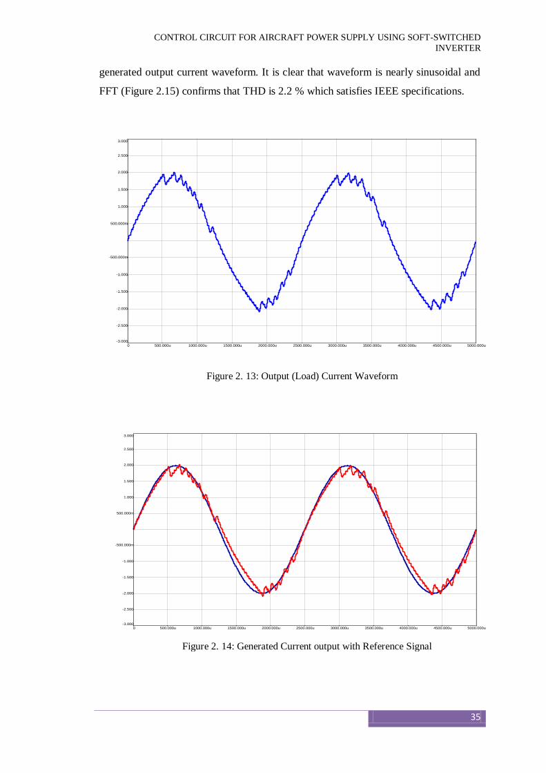
CONTROL CIRCUIT FOR AIRCRAFT POWER SUPPLY USING SOFT-SWITCHED
INVERTER
35
generated output current waveform. It is clear that waveform is nearly sinusoidal and
FFT (Figure 2.15) confirms that THD is 2.2 % which satisfies IEEE specifications.
Figure 2. 13: Output (Load) Current Waveform
500.000m
1.000
1.500
2.000
2.500
-500.000m
-1.000
-1.500
-2.000
-2.500
-3.000
3.000
0 500.000u 1000.000u 1500.000u 2000.000u 2500.000u 3000.000u 3500.000u 4000.000u 4500.000u 5000.000u
500.000m
1.000
1.500
2.000
2.500
-500.000m
-1.000
-1.500
-2.000
-2.500
-3.000
3.000
0 500.000u 1000.000u 1500.000u 2000.000u 2500.000u 3000.000u 3500.000u 4000.000u 4500.000u 5000.000u
Figure 2. 14: Generated Current output with Reference Signal
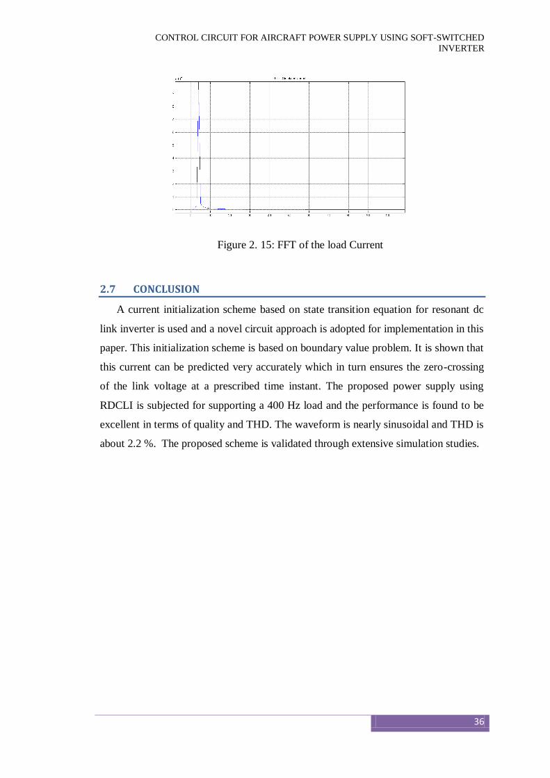
CONTROL CIRCUIT FOR AIRCRAFT POWER SUPPLY USING SOFT-SWITCHED
INVERTER
36
Figure 2. 15: FFT of the load Current
2.7 CONCLUSION
A current initialization scheme based on state transition equation for resonant dc
link inverter is used and a novel circuit approach is adopted for implementation in this
paper. This initialization scheme is based on boundary value problem. It is shown that
this current can be predicted very accurately which in turn ensures the zero-crossing
of the link voltage at a prescribed time instant. The proposed power supply using
RDCLI is subjected for supporting a 400 Hz load and the performance is found to be
excellent in terms of quality and THD. The waveform is nearly sinusoidal and THD is
about 2.2 %. The proposed scheme is validated through extensive simulation studies.

37
POWER LOSS ESTIMATION
HE inspiration for the use of the resonant inverter shoots from an
aspiration to minimize the switching losses in the inverter devices. This
chapter portrays an exhaustive study on losses in the resonant DC link
inverter. Equations for accessing the diverse losses in the resonant DC link inverter
and a corresponding hard switching inverter are developed. Based on these equations,
a design optimization is executed for the DC link inverter to attain the optimum
standards of the link components. Finally, an evaluation of the losses in the resonant
inverter and the hard switching inverter is made.
T
Chapter
3

POWER LOSS ESTIMATION
38
3.1 INTRODUCTION
PWM (Pulse Width Modulation) Inverters and Soft-Switching Inverters (SSI) are
used in power electronics literature extensively. Both classes of inverters find
applications in several domains. Soft-Switching Inverters are developed in recent
times primarily to reduce switching losses. Both PWM and SSI inverters provide a
different advantages vis-à-vis disadvantages which are documented in the literature
[18-25]. In this chapter an attempt is made to evaluate losses in both types of
inverters. This would facilitate for optimum design of link components in the
Resonant DC Link Inverter (RDCLI). Here a detailed analysis of the losses in the
resonant DC link inverter is made. Equations for estimating the various losses in the
resonant DC link inverter and an equivalent hard switching inverter are developed.
Based on these equations, a design optimization is performed for the resonant DC link
inverter to find the optimum values of the link components. Finally, a comparison of
the losses in the resonant inverter and hard switching inverter is made.
3.2 Losses in the Hard-Switching Inverter
The key power losses, in the hard switching inverter, are the conduction and
switching losses in the inverter devices. Occurrence of the conduction losses is due to
the on-state voltage across the device as well as the current flow through the device
striking in chorus. Switching losses are sustained by the concurrent occurrence of
voltage and current on the device while switching. Evaluation of these losses can be
done using simplified device models.
3.2.1 Conduction Losses
To evaluate conduction loss, the device is simplified as a constant voltage drop in
series with a linear resistor. For both IGBTs and diodes, this simplified model is
appropriate. The expression for the on-state voltage of an IGBT and a diode is shown
in Equations 3.1 and 3.2, respectively.
(3.1)
(3.2)
ce q q qV V I R
ak d d dV V I R
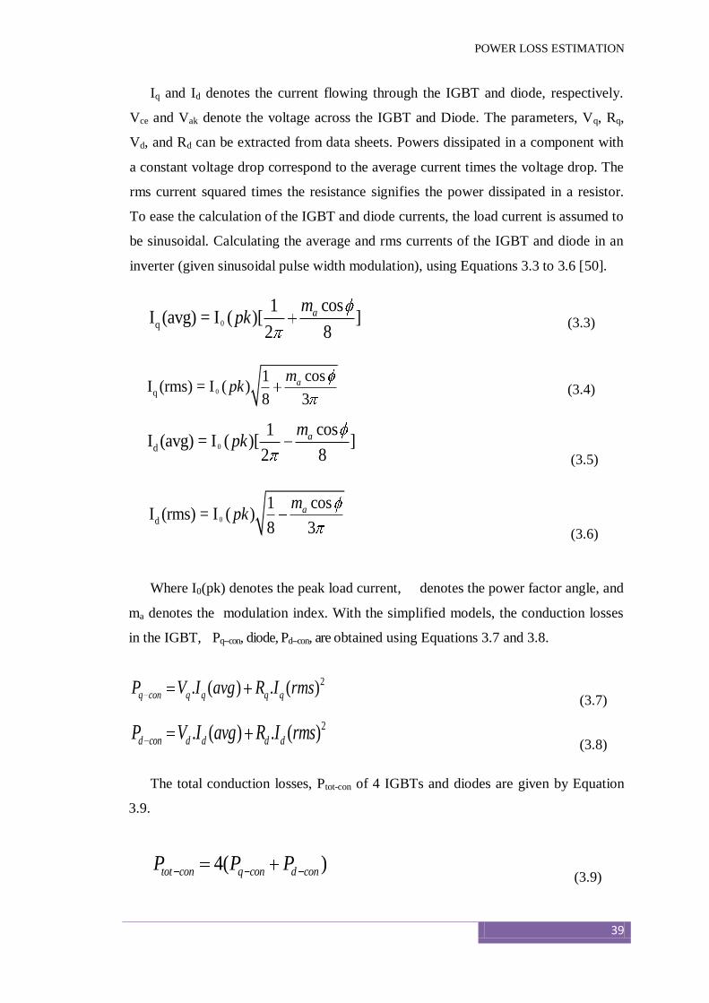
POWER LOSS ESTIMATION
39
Iq and Id denotes the current flowing through the IGBT and diode, respectively.
Vce and Vak denote the voltage across the IGBT and Diode. The parameters, Vq, Rq,
Vd, and Rd can be extracted from data sheets. Powers dissipated in a component with
a constant voltage drop correspond to the average current times the voltage drop. The
rms current squared times the resistance signifies the power dissipated in a resistor.
To ease the calculation of the IGBT and diode currents, the load current is assumed to
be sinusoidal. Calculating the average and rms currents of the IGBT and diode in an
inverter (given sinusoidal pulse width modulation), using Equations 3.3 to 3.6 [50].
(3.3)
(3.4)
(3.5)
(3.6)
Where I0(pk) denotes the peak load current, denotes the power factor angle, and
ma denotes the modulation index. With the simplified models, the conduction losses
in the IGBT, Pq--con, diode, Pd--con, are obtained using Equations 3.7 and 3.8.
(3.7)
(3.8)
The total conduction losses, Ptot-con of 4 IGBTs and diodes are given by Equation
3.9.
(3.9)
0q
cos1I (avg) = I ( )[ ]
2 8
ampk
0q
cos1I (rms) = I ( )
8 3
ampk
0d
cos1I (avg) = I ( )[ ]
2 8
ampk
0d
cos1I (rms) = I ( )
8 3
ampk
2. ( ) . ( )q con q q q qP V I avg R I rms
2. ( ) . ( )d con d d d dP V I avg R I rms
4( )tot con q con d conP P P

POWER LOSS ESTIMATION
40
Evidently, considering device characteristics, the conduction losses are only reliant
on load conditions.
3.2.2 Switching Losses
Three components of the switching losses in the hard switching inverter can be
identified; IGBT turn on losses, IGBT turn off losses, and the losses due to diode
reverse recovery. Evaluation of the switching losses in the hard switching inverter can
be done using the measured values of switching energy from the data sheets.
Generally, data sheets provide the calculated values of turn-on and turn-off energy
(Eon and E0ff) for a conventional test voltage and current (Vtest and Itest). The calculated
values of turn-on energy comprise the losses due to diode reverse recovery. These
standards should be leveled suitably for a specific application using Equation 3.10
[51].
(3.10)
Equation 3.10 represents Vs as the bus voltage, I0(pk) as the peak load current, and
Kg as the correction factor to account for the gate drive impedance. Calculation for
the total switching losses, Ptot-sw, switching inverter can be done using Equation 3.11
[50].
(3.11)
Where fs denotes the PWM switching frequency. Equation 3.12 in the hard
switching inverter as the total losses given in is the sum of the total conduction and
switching losses.
(3.12)
Evidently, from Equation 3.11 the switching losses in the hard switching inverter
are directly related to the PWM switching frequency. Hence due to the switching
losses the achievable switching frequency is thermally limited. Further, from Equation
3.10 the switching energy is proportional to the voltage across the device during
0( )
( ) s
tot g on off
test test
V I pkE K E E
V I
4 tottot sw s
EP f
( )tot tot con tot swP HSI P P
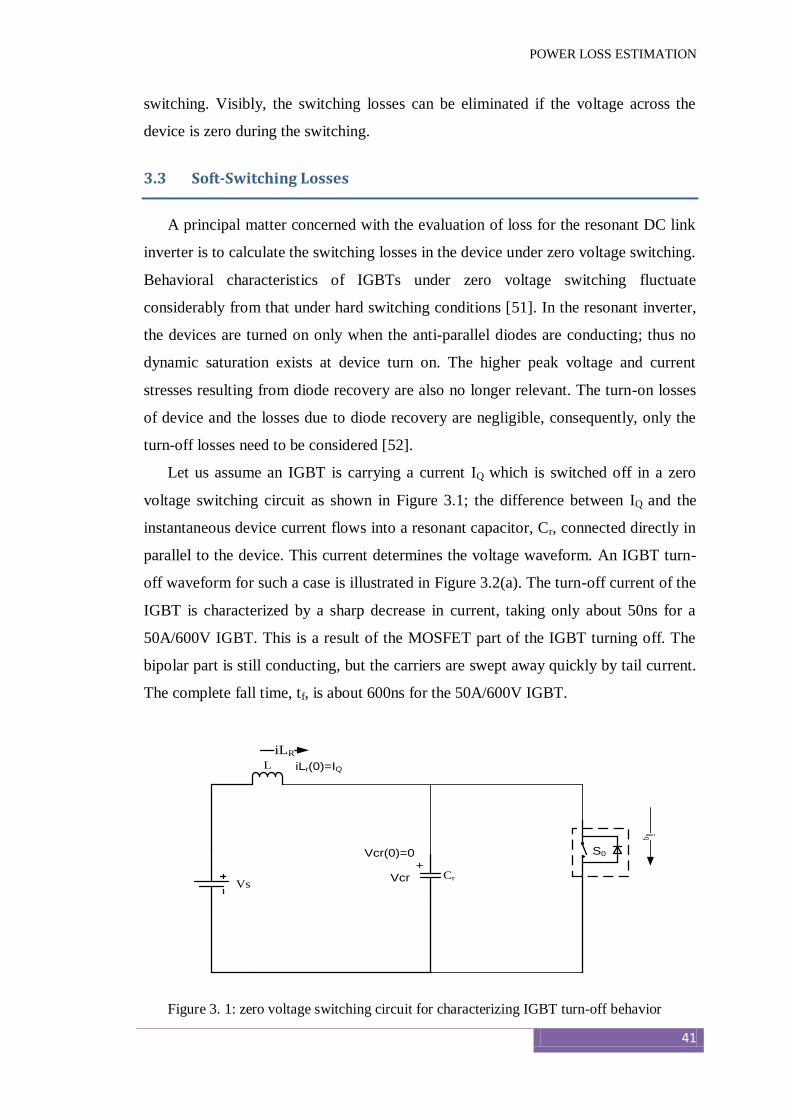
POWER LOSS ESTIMATION
41
switching. Visibly, the switching losses can be eliminated if the voltage across the
device is zero during the switching.
3.3 Soft-Switching Losses
A principal matter concerned with the evaluation of loss for the resonant DC link
inverter is to calculate the switching losses in the device under zero voltage switching.
Behavioral characteristics of IGBTs under zero voltage switching fluctuate
considerably from that under hard switching conditions [51]. In the resonant inverter,
the devices are turned on only when the anti-parallel diodes are conducting; thus no
dynamic saturation exists at device turn on. The higher peak voltage and current
stresses resulting from diode recovery are also no longer relevant. The turn-on losses
of device and the losses due to diode recovery are negligible, consequently, only the
turn-off losses need to be considered [52].
Let us assume an IGBT is carrying a current IQ which is switched off in a zero
voltage switching circuit as shown in Figure 3.1; the difference between IQ and the
instantaneous device current flows into a resonant capacitor, Cr, connected directly in
parallel to the device. This current determines the voltage waveform. An IGBT turn-
off waveform for such a case is illustrated in Figure 3.2(a). The turn-off current of the
IGBT is characterized by a sharp decrease in current, taking only about 50ns for a
50A/600V IGBT. This is a result of the MOSFET part of the IGBT turning off. The
bipolar part is still conducting, but the carriers are swept away quickly by tail current.
The complete fall time, tf, is about 600ns for the 50A/600V IGBT.
Figure 3. 1: zero voltage switching circuit for characterizing IGBT turn-off behavior
Cr
L
S0
VsVcr
+
iLR
iLr(0)=IQ
Vcr(0)=0
iq
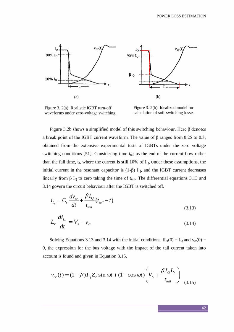
POWER LOSS ESTIMATION
42
Figure 3.2b shows a simplified model of this switching behaviour. Here β denotes
a break point of the IGBT current waveform. The value of β ranges from 0.25 to 0.3,
obtained from the extensive experimental tests of IGBTs under the zero voltage
switching conditions [51]. Considering time ttail as the end of the current flow rather
than the fall time, tf, where the current is still 10% of IQ, Under these assumptions, the
initial current in the resonant capacitor is (1-β) IQ, and the IGBT current decreases
linearly from β IQ to zero taking the time of ttail. The differential equations 3.13 and
3.14 govern the circuit behaviour after the IGBT is switched off.
(3.13)
(3.14)
Solving Equations 3.13 and 3.14 with the initial conditions, iLr(0) = IQ and vcr(0) =
0, the expression for the bus voltage with the impact of the tail current taken into
account is found and given in Equation 3.15.
(3.15)
( )r
QcrL r tail
tail
Idvi C t t
dt t
rL
r s cr
diL V v
dt
( ) (1 ) sin (1 cos )Q r
Scr Q r
tail
I LVv t I Z t t
t
Figure 3. 2(a): Realistic IGBT turn-off
waveforms under zero-voltage switching,
Figure 3. 2(b): Idealized model for
calculation of soft-switching losses
10% IQ
(a) (b)
Ttail
βIQ
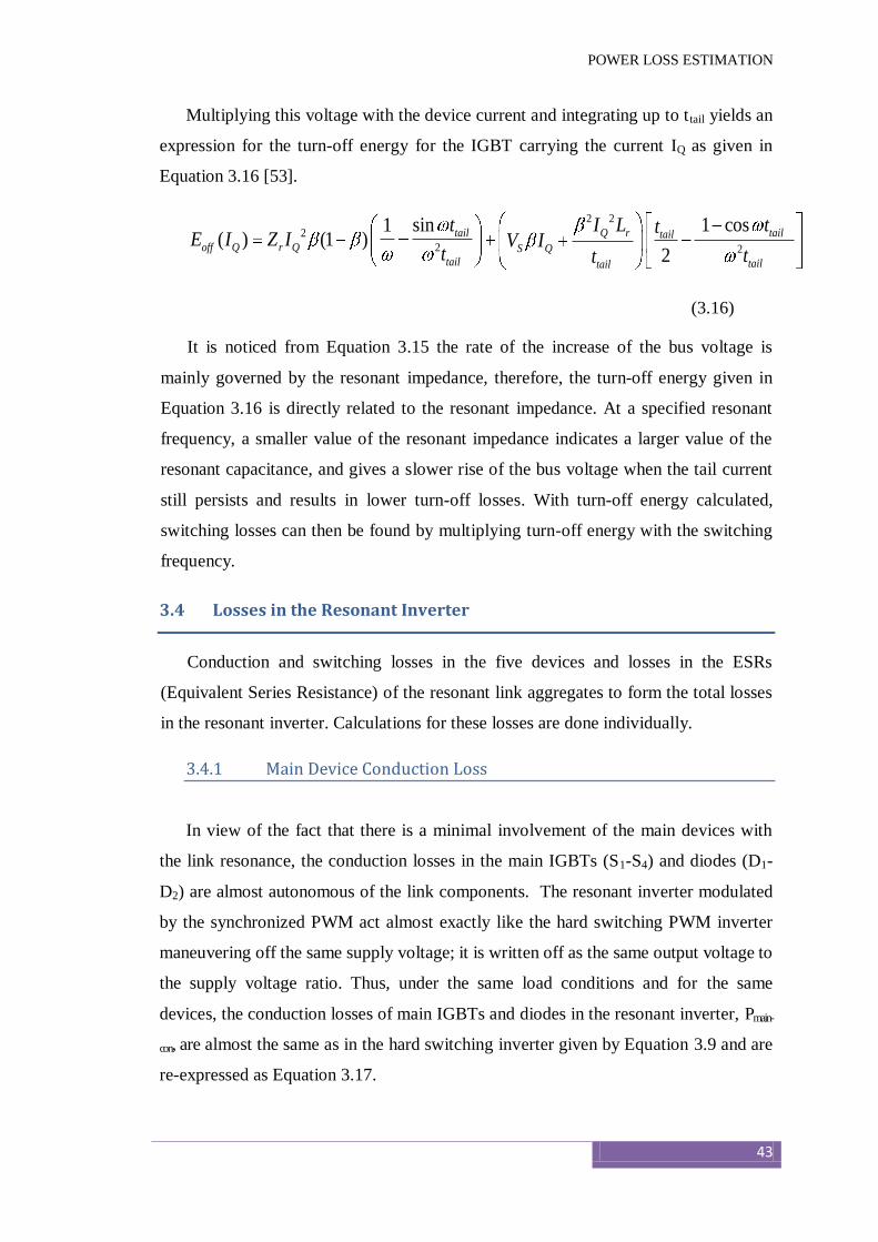
POWER LOSS ESTIMATION
43
Multiplying this voltage with the device current and integrating up to t tail yields an
expression for the turn-off energy for the IGBT carrying the current IQ as given in
Equation 3.16 [53].
(3.16)
It is noticed from Equation 3.15 the rate of the increase of the bus voltage is
mainly governed by the resonant impedance, therefore, the turn-off energy given in
Equation 3.16 is directly related to the resonant impedance. At a specified resonant
frequency, a smaller value of the resonant impedance indicates a larger value of the
resonant capacitance, and gives a slower rise of the bus voltage when the tail current
still persists and results in lower turn-off losses. With turn-off energy calculated,
switching losses can then be found by multiplying turn-off energy with the switching
frequency.
3.4 Losses in the Resonant Inverter
Conduction and switching losses in the five devices and losses in the ESRs
(Equivalent Series Resistance) of the resonant link aggregates to form the total losses
in the resonant inverter. Calculations for these losses are done individually.
3.4.1 Main Device Conduction Loss
In view of the fact that there is a minimal involvement of the main devices with
the link resonance, the conduction losses in the main IGBTs (S1-S4) and diodes (D1-
D2) are almost autonomous of the link components. The resonant inverter modulated
by the synchronized PWM act almost exactly like the hard switching PWM inverter
maneuvering off the same supply voltage; it is written off as the same output voltage to
the supply voltage ratio. Thus, under the same load conditions and for the same
devices, the conduction losses of main IGBTs and diodes in the resonant inverter, Pmain-
con, are almost the same as in the hard switching inverter given by Equation 3.9 and are
re-expressed as Equation 3.17.
2 2
2
2 2
sin 1 cos1( ) (1 )
2
tail tailQ r tailoff Q r Q S Q
tail tailtail
t tI L tE I Z I V I
t tt
POWER LOSS ESTIMATION
44
(3.17)
3.4.2 Main Device Switching Loss
Primarily the switching losses in the main devices depend on the resonant
capacitor and indirectly on the resonant inductor. Turned- off the peak load current,
I0(pk), in a main device, the resulting turn-off energy, Eoff[I0(pk)], can be calculated
using Equation 3.16 with IQ replaced by IQ(pk). In the resonant inverter, the switching
frequency of the main devices varies and depends mainly on the resonant frequency
fr, whenever the output voltage is zero volts, highest switching frequency occurs, and
equals the resonant frequency. The average switching frequency of the main devices
equals half the resonant frequency [54]. The switching losses in the four main devices,
Pmain-sw, can be found using Equation 3.18.
(3.18)
3.4.3 Equivalent Series Resistance (ESR) Losses
Since the current circulates in the resonant link, losses are gained in ESR
elements. The ESR losses in the resonant capacitor can be ignored since the resonant
capacitor has a very high quality factor. Also, the ESR losses in the clamp capacitor
can be neglected since the rms current in the clamp capacitor is very low. Hence, only
the ESR losses in the resonant inductor need to be considered.
When the resonant inverter operates with a load, the inductor current oscillates
tracking the changes of the inverter DC current. The inductor current waveform [55]
is given by Equation 3.19
(3.19)
The ESR value of the resonant inductor is dogged by the inductor quality factor
Q. The losses in the resonant inductor, PLr, are then achieved using Equation 3.20.
(3.20)
4( )main con q con d conP P P
04 [ ( )]2
rmain sw off
fP E I pk
12 0 12
12
1( ) [ ]r sI t I V
2
r
rL r
ZP I
Q

POWER LOSS ESTIMATION
45
The total losses in the Resonant DC link inverter can now be calculated by adding
up the main device losses and the resonant inductor losses, and are represented in
Equation 3.21.
(3.21)
3.5 System Optimization
The design of the resonant DC link inverter initiates with the selection of the
switching devices. Given the device characteristics, the resonant components Lr and
Cr can then be preferred to minimize the total losses.
Five-pack 50A/600V IGBT modules (Mitsubishi) are chosen as the main devices
of the inverter stage and device of the resonant link.
Limitations to the maximum resonant frequency achievable in the real circuit by
several factors include device switching characteristics, thermal constraints, and
availability of the passive components [56]. To modulate the inverter for the
prototype resonant DC link inverter, a synchronized PWM scheme is used. In this
scheme the PWM signals are sampled at the resonant frequency and then
synchronized to the zero crossing of the bus voltage. For example, hysteresis bang-
bang control is used in PWM inverters for current control within the inverter;
however RDCLI uses zero hysteresis bang-bang control; if switches are switched only
when the voltage/current is zero and not necessarily when bang-bang controller acts.
In order to preserve the well-defined switching pattern of the PWM signals,
simulations show that a resonant frequency of about 5 times of the PWM switching
frequency is adequate. A resonant frequency of 25-40 kHz is chosen for the design of
the link components, considering a maximum PWM switching frequency of 5-8 kHz.
In this thesis we are designing a 400 Hz power supply using Soft-Switched Inverter.
In the PWM case for more than 100 KVA load, the switching frequency is limited to
5 – 8 kHz and if we further increase the frequency the product of frequency and
Power loss will be more and more heat will be generated. So considering this
condition we are incorporating Soft-Switched based Inverter and whose switching
frequency range is 5 - 8 times of PWM frequency, which is 25 – 40 kHz. For this
reason we have taken a random frequency of 28 kHz. If the resonant impedance is
known, considering the resonant frequency, the values of the resonant components
can be determined. Depending upon the market availability we purchased a poly-
rtot main con main sw LP P P P
POWER LOSS ESTIMATION
46
propylene capacitor of 1 µF. So based on above simulation studies and power loss
estimation, we calculate the inductor value to be 33 µH. Though different sets or
combination Resonant capacitor and inductor can be tested and verified.
Under no load in the resonant link, losses are regulated by the resonant current,
which is nearly verified by Vs/Zr. A lower current in the resonant link and lower
losses is resulted by a larger value of the resonant impedance. With the resonant
inverter under load, the load-dependent DC current flows through the resonant
inductor. A larger value of the resonant impedance suggests a larger value of resonant
inductance, and this in turn causes more ESR losses in the inductor since more turns
are required to build the inductor [Fig. 3.3]. On the other hand when the inverter
devices are switched off, for the inverter stage, a small value of the resonant
impedance is desirable to make the bus voltage increase slowly. Evidently, an
optimum value of the resonant impedance exists, which gives the lowest losses in the
resonant DC link inverter.
A computer program has been developed, based on the equations derived in the
previous sections, to calculate the total losses in the resonant inverter and hard
switching inverter. Figure 3.3 shows design optimization curves for the resonant DC
link inverter using IGBTs operated off the supply voltage of 230V. With the intention
of calculating loss, the load is assumed to be a sinusoidal current source of 25A rms
with a power factor of 0.86 and a modulation index of 0.65. A realistic inductor
quality factor of 167 is used for the loss calculations. The model parameters,
Vq=0.78V and Rq=0.011Ω, are used to calculate the conduction losses of the IGBTs.
The model parameters, Vd=1.0V and Rd=0.009Ω, are used to calculate the conduction
losses of the diodes. The values, β=0.3 and ttail=515ns, are used to calculate the soft
switching losses. Loss calculations are executed for the different values of the
resonant impedance while the resonant frequency is stable at 28 kHz.
It is observed from Figure 3.3 that with a decrease in the resonant impedance the
losses in the main devices and resonant inductor decrease, and hence total loss reduce.
In particular, the losses in the resonant inductor increase dramatically for the
impedance values below 5.8 Ω. The load-dependent losses in the ESR of the inductor
seem to be insignificant given a high quality factor, as can be seen there is only a
small increase of the losses in the inductor while the value of the resonant impedance
is increased. Examining the curve of the total losses, the trade-off between the link
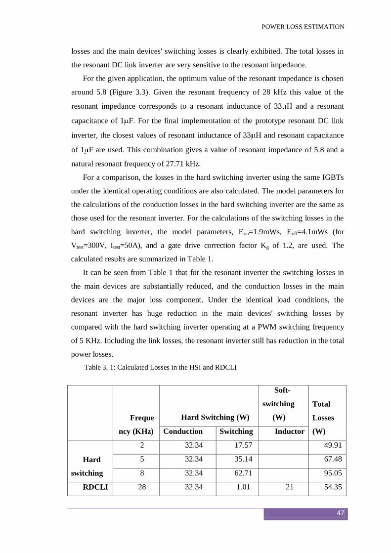
POWER LOSS ESTIMATION
47
losses and the main devices' switching losses is clearly exhibited. The total losses in
the resonant DC link inverter are very sensitive to the resonant impedance.
For the given application, the optimum value of the resonant impedance is chosen
around 5.8 (Figure 3.3). Given the resonant frequency of 28 kHz this value of the
resonant impedance corresponds to a resonant inductance of 33 H and a resonant
capacitance of 1 F. For the final implementation of the prototype resonant DC link
inverter, the closest values of resonant inductance of 33 H and resonant capacitance
of 1 F are used. This combination gives a value of resonant impedance of 5.8 and a
natural resonant frequency of 27.71 kHz.
For a comparison, the losses in the hard switching inverter using the same IGBTs
under the identical operating conditions are also calculated. The model parameters for
the calculations of the conduction losses in the hard switching inverter are the same as
those used for the resonant inverter. For the calculations of the switching losses in the
hard switching inverter, the model parameters, Eon=1.9mWs, Eoff=4.1mWs (for
Vtest=300V, Itest=50A), and a gate drive correction factor Kg of 1.2, are used. The
calculated results are summarized in Table 1.
It can be seen from Table 1 that for the resonant inverter the switching losses in
the main devices are substantially reduced, and the conduction losses in the main
devices are the major loss component. Under the identical load conditions, the
resonant inverter has huge reduction in the main devices' switching losses by
compared with the hard switching inverter operating at a PWM switching frequency
of 5 KHz. Including the link losses, the resonant inverter still has reduction in the total
power losses.
Freque
ncy (KHz)
Hard Switching (W)
Soft-
switching
(W)
Total
Losses
(W) Conduction Switching Inductor
Hard
switching
2 32.34 17.57 49.91
5 32.34 35.14 67.48
8 32.34 62.71 95.05
RDCLI 28 32.34 1.01 21 54.35
Table 3. 1: Calculated Losses in the HSI and RDCLI
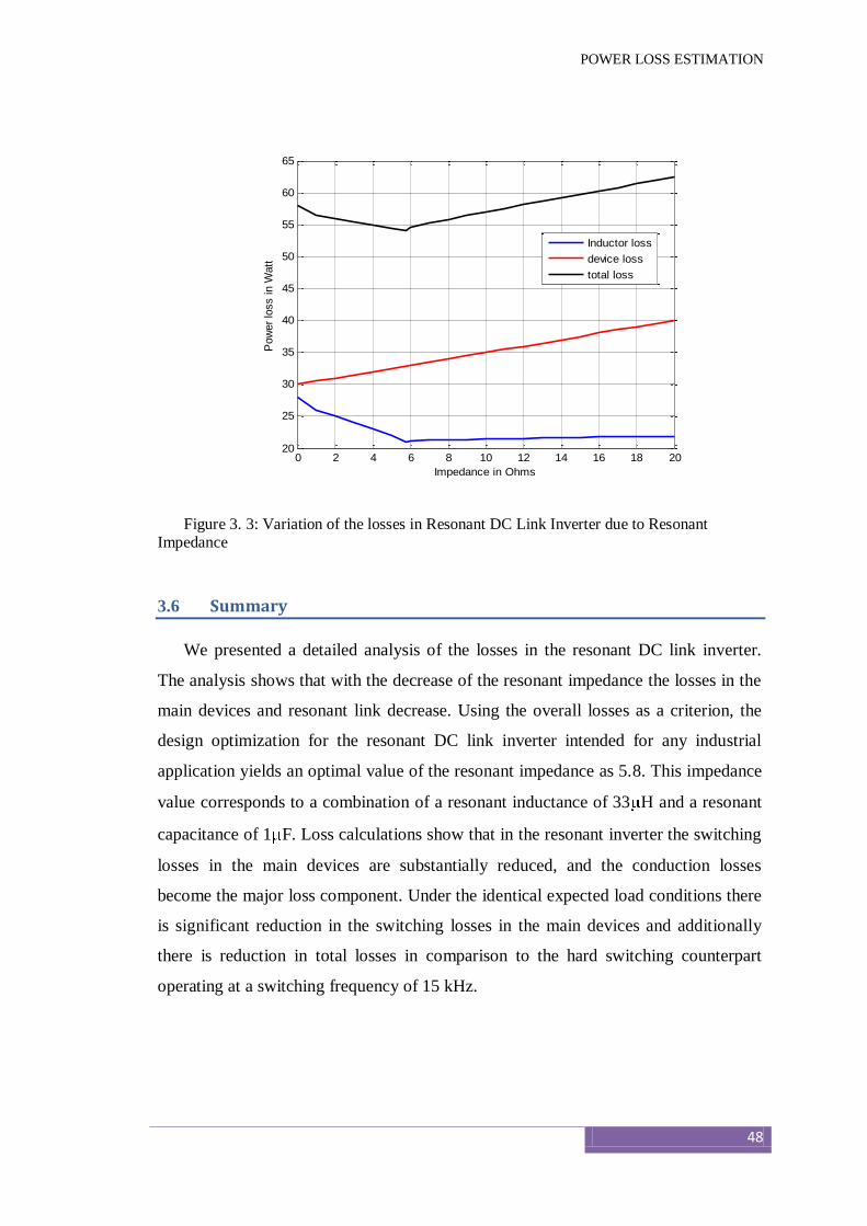
POWER LOSS ESTIMATION
48
Figure 3. 3: Variation of the losses in Resonant DC Link Inverter due to Resonant Impedance
3.6 Summary
We presented a detailed analysis of the losses in the resonant DC link inverter.
The analysis shows that with the decrease of the resonant impedance the losses in the
main devices and resonant link decrease. Using the overall losses as a criterion, the
design optimization for the resonant DC link inverter intended for any industrial
application yields an optimal value of the resonant impedance as 5.8. This impedance
value corresponds to a combination of a resonant inductance of 33 H and a resonant
capacitance of 1 F. Loss calculations show that in the resonant inverter the switching
losses in the main devices are substantially reduced, and the conduction losses
become the major loss component. Under the identical expected load conditions there
is significant reduction in the switching losses in the main devices and additionally
there is reduction in total losses in comparison to the hard switching counterpart
operating at a switching frequency of 15 kHz.
0 2 4 6 8 10 12 14 16 18 2020
25
30
35
40
45
50
55
60
65
Impedance in Ohms
Pow
er
loss in W
att
Inductor loss
device loss
total loss

49
EXPERIMENTAL SETUP
The experimental set-up used for experimental verification of soft-switched
Inverter based 400 Hz power supply principle is discussed in this chapter. The
objective is to demonstrate the performance of single-phase soft-switched Inverter
based 400 Hz power supply design. A resonant link is fabricated which is controlled
by the proposed current initialization scheme that includes PC interface. In this
chapter the details of fabrication of various control cards, the power circuit, the drive
circuit of the inverter and the PC interface are given.
The power circuit of the RDCLI based soft-switched Inverter is shown in Figure
4.1. The ac supply supplies the non-linear load. The capacitor (Cf) in the circuit is the
energy storing capacitor. The diode-bridge and the inductor are used for pre-charging.
Once charging is done, this part of the circuit is opened using a mechanical switch
MS-1. The block diagram of the control circuit of RDCLI is shown in Figure 4.2.
Switching in this case can only be done when the link voltage is zero. Just before the
zero voltage condition occurs, generated reference currents are compared with their
Chapter
4

50
corresponding actual values to generate these error signals. This signal is given to the
current regulator circuit such that current regulator provides the required current.
Current initialization is carried out as described in current initialization circuit for
ZVS purpose.
4.1 COMPONENTS
The power circuit of the resonant link is shown in Figure 4.1. To pre-charge the
capacitor Cf a diode-bridge is used along with a filter inductor. Through the diode-
bridge we can build up the voltage Vdc across Cf which will act as a supply for the
resonant link. The resonant link consists of inductor L and capacitor C. In order to get
high Q factors for the inductors at high resonant frequencies a litz-wire air core
inductor is fabricated. The design and fabrication of these air core inductors [58] are
given below. The resonant link capacitor is of polypropylene type while the filter
capacitor Cf is electrolytic type. The link is designed to operate at a frequency of 28
kHz for which the various resonant component values are L = 33 H, C = 1 F, Cf =
3000 F, Q = 167, Vdc = 30 V. A careful physical layout of the resonant components
has been made. It is to be noted that a variable external resistance Rext is added in
series with the shorting switch S0. This is done for protection and is used during the
starting stage. Once the link starts up and operational this is reduced to zero.
The components needed to realize a resonant DC link inverter include the resonant
inductor, resonant capacitor, and switching devices for the inverter stage. The design
and selection of these components are described in this section.
4.1.1 Resonant Inductor
The resonant inductor carries the inverter DC current and the resonant current.
The average value of the inverter DC current is dependent on the load conditions,
whereas the resonant current is dependent on the resonant link parameters and has a
resonant frequency of about 28 kHz. Further, the amplitude of the resonant current is
even larger than the average value of the inverter DC current.

EXPERIMENTAL SETUP
51
DESIGN OF RESONANT INDUCTOR
The inductors used in the resonant link inverters have to carry large circulating
currents at high resonant frequencies. In order to reduce the skin effect and to get
good quality factor use of Litz wire is recommended. Since litz wires of large current
ratings are not easily available, these have been fabricated in the laboratory according
to the following definition.
Litz Wire: If the conductor is broken into many small strands, twisted about 10 turns per
feet and each strand insulated from each other, the skin effect is lessened. Such wire is known
as litz wire.
For single layered coil inductance L is given by [58]
Where n = number of turns.
a = radius of the coil in cms.
b = length of the coil in cms.
k = function of (2a/b)
Design of Inductor L:
Former: 11.5 cm dia, 14 cms long, air core
Wire: 29 SWG enamelled (100 strands each)
Number of turns: 27
Current Rating: 40 A
Value = 33 H (measured)
The designed value of the inductor is approximately same. In our design
kb
naL
220395.0

EXPERIMENTAL SETUP
52
a = 6.05 cm
b = 14.5 cm
n = 25
k = 0.7258
Substituting these values we will get almost the same result.
Variation of Q factor with Frequency
It may be noted that these values are obtained through LCR meter. In the
experimental setup the value of Q is taken to be 167 as Q has changed by the other
circuit parameters and connecting wires.
In practice, to avoid the eddy losses that may be caused by the fringing flux across
the air gap, any metal objects (like bolts) required for mechanical assembly of the
resonant inductor should not be located in the vicinity of the air gap.
4.1.2 Resonant Capacitor
Metalized polypropylene capacitors are commonly used as the IGBT snubber
capacitors in the power electronic field. The advantages include low loss, high current
ratings, high reliability, small size and low cost [60]. In the resonant DC link inverter,
Frequency in
kHz
Q Factor
5 70
10 94
20 149
50 162
100 175

EXPERIMENTAL SETUP
53
the resonant capacitor can also be regarded as a snubber, which is periodically reset
by resonating with the resonant inductor [61].
Polypropylene film capacitors (MPTA, VC) were chosen to constitute the resonant
capacitor in the prototype resonant inverter mainly due to low dielectric loss. The
selected film capacitor has a rated capacitance value of 1 F and a rated working
voltage of 2000V DC.
4.1.3 Switching Devices
The current ratings of the switching devices in the prototype resonant inverter
were determined based on such an arrangement in which the resonant inverter is
connected to loads (e.g., induction motors, allowing a torque controller to be used to
control each induction motor). Line current drawn by one induction motor is about
25A rms at rated torque and up to 75A rms at peak torque [59]. Thus the selected
switching devices should be able to handle a peak current of 106A.
It is highly desirable that the 600V devices can be used as the switching devices
for the resonant inverter, as a 600V device has a lower saturation voltage, therefore
lower conduction losses compared to a 1200V device. This gives an adequate margin
for 600V devices.
From the above considerations of current and voltage ratings, four-pack 150A/600V
IGBT modules (CM150DU-12H, MITSUBISHI) including fast free-wheel diodes
were selected as the switching devices of the resonant inverter.
Table 4.1 gives a summary of the components used to implement the prototype
resonant DC link inverter.
Table 4. 1: Components for the Prototype Resonant DC Link Inverter
Inverter
devices 150A/600V IGBT module per phase leg
Resonant
inductor 33 H, air core, Litz wire
Resonant
capacitor 1 F, 1000VDC polypropylene capacitors
EXPERIMENTAL SETUP
54
4.2 CURRENT INITIALIZATION CIRCUIT
With these values of inductor and capacitor the un-damped oscillation time is
42.75 s. Therefore, the resonant cycle time T is chosen to be 37.5 s taking into
account the finite Q-factor of the coil.
The block diagram of the proposed current initialization scheme is shown in
Figure 2.9. The corresponding control circuit is shown in Figure 4.3.
A personal computer (PC) along with its associated high-speed analog-to-
digital converter (ADC) and digital-to-analog converter (DAC) is used for the
computation of the initial current from equation (2.4). In this equation , and
are constants that are dependent on the circuit parameters and the time T. These
are pre-computed and stored. The load current ( ) and the dc voltage Vdc are
measured through Hall-effect sensors (HE-1 and HV-1 respectively in Figure 4.1) at
the start of every resonant cycle (e.g. in Figure 2.4) and are converted through
ADC. These measured values along with the constants mentioned above are used for
the computation of the initial current. This process is repeated for every resonant
cycle. It is to be noted that the computation here is fairly simple and can also be
achieved through a hardware configuration. However, the use of PC makes the control
circuit much more flexible than a hardwired circuit. Furthermore, due to the presence
of the PC, the delays and tolerances of the actual circuit can also be taken into
account. An accurate zero-voltage switching can be obtained in the experiment.
As mentioned in Chapter 2 (Section 2.2) there are two methods of obtaining time
t for which the capacitor should be shorted, of which we use method-2. As soon as
the required initial current is computed in the PC, it is converted into an analog signal
through a DAC. The computation time required is much smaller than the resonant
cycle time . This signal is then available to the comparator for comparison with the
actual link current. The link current is monitored continuously through a Hall-effect
current sensor (HE-1 shown in Figure 4.1). Let us discuss the operation of the circuit
in Figure 4.3. When the link current becomes equal to the required initial current, the
comparator output (Y) becomes zero. The signal Y is conditioned by protection
circuit (Figure 4.4) and then the output Z= Y Pt is used for clearing the J-K flip-flop
(74LS76 in Figure 4.3). Under normal condition Z= Y, as protection signal Pt = 1.
Once this flip-flop is cleared, its output (Q) becomes zero and becomes one. This
11 21
21
0I
2t
T
Q

EXPERIMENTAL SETUP
55
is then used for switching off through a buffer. Simultaneously, the inverted
output ( ) of the J-K flip-flop is used for triggering the mono-stable (7555 in Figure
4.3) through an inverting buffer. The mono-stable timing is designed for a pulse width
of T=37.5 s. After this time elapses, the negative going edge of the mono-stable
output is used to clock the J-K flip-flop. This forces the output of the flip-flop to one
and consequently the shorting switch is turned on.
Through the above scheme, the zero-voltage switching is obtained. It is to be
noted that during the time when S0 is on, the switching transitions of the switches S1-
S4 take place. To ensure that the switches S1-S4 are turned on or off only during this
prescribed interval, the gating of S1-S4 are conditioned by the output Q of the J-K flip-
flop. Further note that the configuration of the switches S1-S4 at a particular resonant
cycle is dependent on the load connected to the output of the inverter. It is to be noted
that the J-K flip-flop is cleared under two conditions. One is the usual clearing as
explained already in every resonant cycle. The other is under fault condition. If there
is a fault, the resonant circuit must be stopped. In that case the protection circuit gives
Pt = 0 and signal Z is forced to zero. The switch S0 is therefore opened permanently so
that the link voltage and link current will gradually decay to zero due to the internal
resistance of the resonant coil. The output of the mono-stable is also used for the
starting ADC. When this is triggered through , its output goes high. This is also the
onset of the resonant cycle. This positive going edge (through buffer CD 4049) is
used as a signal to the PC interface card such that the ADC starts sampling I0 and
Vdc.
4.3 CURRENT REGULATOR CIRCUIT
The current regulator control circuit is shown in Figure 4.4. The switching of the
devices is synchronized to the zero crossings of the link voltage so as to obtain ZVS.
The resonant dc link inverter and controller is configured to regulate its current so as
to match the current reference. As mentioned earlier the mono-stable of Figure 4.3 is
triggered at the onset of a resonant cycle. This then goes zero after 37.5 s elapses.
The negative going edge of the mono-stable output is used for clocking the J-K flip-
flop. This force the output of the flip-flop to one and consequently the shorting switch
S0 is turned on.
0S
Q
0S
Q

EXPERIMENTAL SETUP
56
The same signal is used to clock the D-flip-flop (74F74) in Figure 4.4 so that
the synchronization is obtained. The comparator compares the actual inverter current
(HE-2) with the reference of the inverter (obtained from the PC). Based on the output
of the comparator (LM-311), a switching decision has to be taken. This output is fed
to the D input of the D latch. However, the output of the D flip-flop remains unaltered
till the next sampling point is reached. The sampling point is the point when resonant
link voltage goes zero. At this sampling point if the output current is lower, then a
positive pulse is given to increase the output current and vice-versa. However, this
pulse is not directly given as seen in Figure 4.4. It is ensured that the outgoing
switches are turned off first and then the incoming switches are turned on. This is
achieved via mono-stable 74123 and AND gate 7408. Therefore a change from 0 to 1
in the 74F74 output is delayed by 1 s where as a change from 1 to 0 in the 74F74
output is passed immediately.
For the protection of both resonant link and the current regulator a protection
scheme is devised in this circuit. The load current is not allowed to be more than 4 A
in either direction. This is done via two comparators. One comparator is set at 4 A and
the other comparator is set at - 4 A. The actual current in the load circuit is compared
with these references. Once the current is beyond limits of 4 A, one of the
comparator output goes zero. This is then used for clocking a negative edge triggered
J-K flip-flop. Therefore under normal conditions the output (Pt) of this J-K will be
1, this will go zero the moment current limit exceeds. This signal is used for blocking
the gate signals. Manual resetting of the J-K flip-flop is required to clear the fault.
The signals derived for switches are transmitted for gate drive circuit after
being ANDed with current limit control signals. There is also a manual start/stop
switch through which the circuit can be stopped at any time. The gating signals are
also ANDed with the start/stop signals. Therefore under normal conditions the signals
for switches S1-S4 are passed immediately.
But under fault conditions these signals are blocked. This is achieved through
AND gates 7408. The comparator output obtained from resonant link control circuit is
also ANDed with this current limit control. In the event of a fault the J-K in current
initialization circuit is cleared so that the switch S0 is opened.
Q
41 SS

EXPERIMENTAL SETUP
57
4.4 BLANKING CIRCUIT
The circuit is shown in Figure 4.4. The task is to compute current error and generate
switching signals for the inverter so as to regulate the error within the hysteresis band.
The blanking circuit uses this signal to generate switching signals for all four
switches. It is to be ensured that the outgoing switches are turned off first. The
incoming switches are then turned on. Therefore a change from 0 to 1 in the 7400
output is delayed by 1 s where as a change from 1 to 0 in the 74F74 output is passed
immediately. This is achieved via mono-stable 74123 and AND gate 7408. It is to be
noted that this 1 s delay is sufficient to ensure that IGBTs are turned off. Otherwise
two switches in the same leg will be turned on resulting shorting of the dc bus. This is
commonly known as shoot-through fault and this is avoided using this lockout
scheme. A hall-effect current sensor (HE-2) is used for the measurement of actual
load current. This signal is then compared with the references already generated.
Based on the error signal a particular switch pair is fired and the other pair is turned
off. It may be noted that when there is no need for changing the status of the switches
the RS Latch holds the old status.
4.5 RESONANCE INITIATION
After the resonant inverter power-on, the resonant capacitor voltage is equal to the
DC supply voltage and no energy is stored in the resonant inductor, so that the bus
voltage can neither resonate to the clamping voltage nor to zero. The link resonance
has to be initiated manually by producing an initial downward swing of the bus
voltage.
This is accomplished by generating an initial inductor charging pulse, Pinitial, to
turn on all the inverter devices for a very short period.
Figure 4.6 shows the circuit for initiating the link resonance. Once a "START"
button is pressed, a pulse is generated at pin 6 of (4098-A, Dual Mono-stable). The
latch (4043) catches the leading edge of this pulse, and the output of this latch is used
to shut down the pre-charge circuit. At the trailing edge of this pulse, the initial
inductor charging pulse, Pinitial, is produced at pin 10 of 4098-B and sent to the gate
drives to short the bus initially. Resistors R2 and C2 control the pulse width of Pinitial.

EXPERIMENTAL SETUP
58
4.6 IGBT GATE DRIVE CIRCUIT
The circuit is shown in Figure 4.5. A gate-drive circuit is designed in the similar
lines as in [50]. The over current –protection feature is added here. The protection
scheme is based on the fact that the drain-source voltage of IGBT increases with drain
current for a given gate-source voltage. The potentiometer P2 shown in the figure is
set such that the voltage at variable point is one diode drop more than the drain source
voltage corresponding to the peak value of the normal drain current. Activation of
protection circuit is delayed by a RC circuit. As long as the drain current is within the
normal limit, the drive signal is transmitted to the gate. When the current exceeds its
limits, the protection logic inhibits the drive signal from reaching the gate, and a fault
indication is given. The fault indication persists as long as the turn-on process is
present. An indication is also given in case of a turn-on failure.
4.7 PC INTERFACE CIRCUIT
For proposed current initialization scheme a PC is used as discussed earlier.
Essentially the load current seen by resonant link are taken which are digitized using
ADCs and then these data are used for computation. Once the computation is over, the
required initial current value (through DAC) is sent to the current initialization circuit
as shown in Figure 4.2 Figure 4.3. Details of the interface card are presented in
appendix A. Here LabVIEW programming is used for communicating ADC and DAC
via PC and Data Acquisition Card. The programming is as shown in Figure 4.7.
4.8 COMPACT RIO FPGA
Here we are replacing PC with FPGA, which is having Real time control and
ADC/DAC. The proposed block diagram is shown in Figure 4.13. Figure 4.8 and 4.9
displays the LabVIEW programming for controlling the real time controller and
communication with the ADC and DAC. Compact RIO with Hardware circuit
connection is shown in Figure 4.14. The complete datasheet of the Compact RIO is
given in appendix B. The corresponding load current after connecting CRIO is given
in Figure 5.9.

EXPERIMENTAL SETUP
59
4.9 CONCLUSIONS
In this chapter, the resonant inductor has been designed based on an available core and
Litz wires. The designed resonant inductor has low winding losses and relatively large core
losses due to the overly large core and the limited number of turns, but it is still acceptable for
the resonant inverter application. In this chapter the details of different circuits that are
fabricated is discussed. The photographs of the laboratory set up are shown in Figure 4.7
through 4.14.
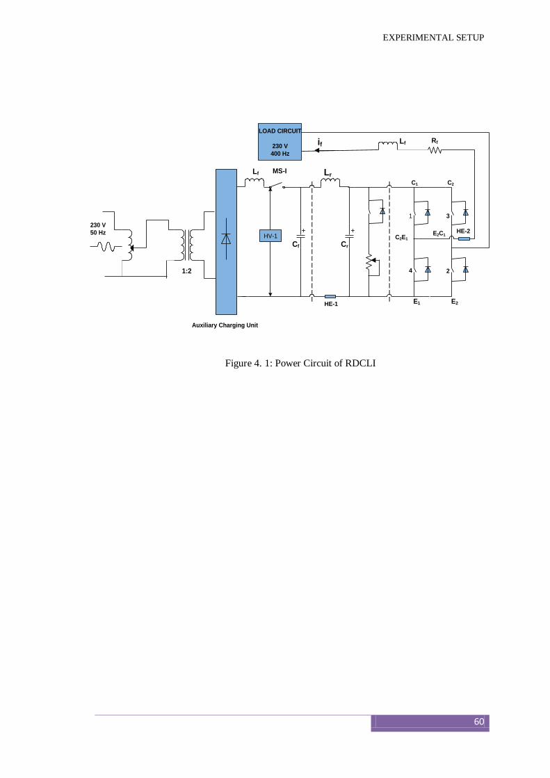
EXPERIMENTAL SETUP
60
Figure 4. 1: Power Circuit of RDCLI
230 V
50 Hz
Lf MS-I Lr
1:2
Auxiliary Charging Unit
HV-1+
Cf
+
Cr
1
4 2
3
C1
E1
C2
E2HE-1
HE-2C2E1
E2C1
LOAD CIRCUIT
230 V
400 Hz
Lf Rfif
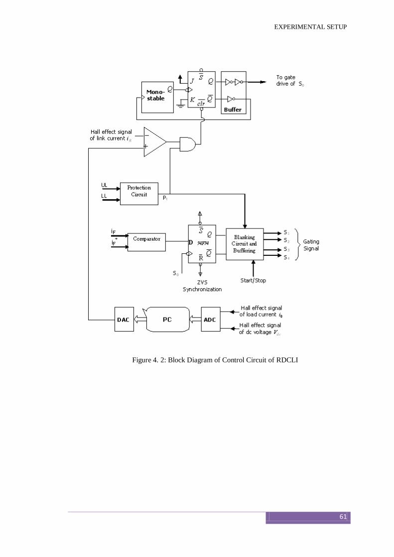
EXPERIMENTAL SETUP
61
Figure 4. 2: Block Diagram of Control Circuit of RDCLI
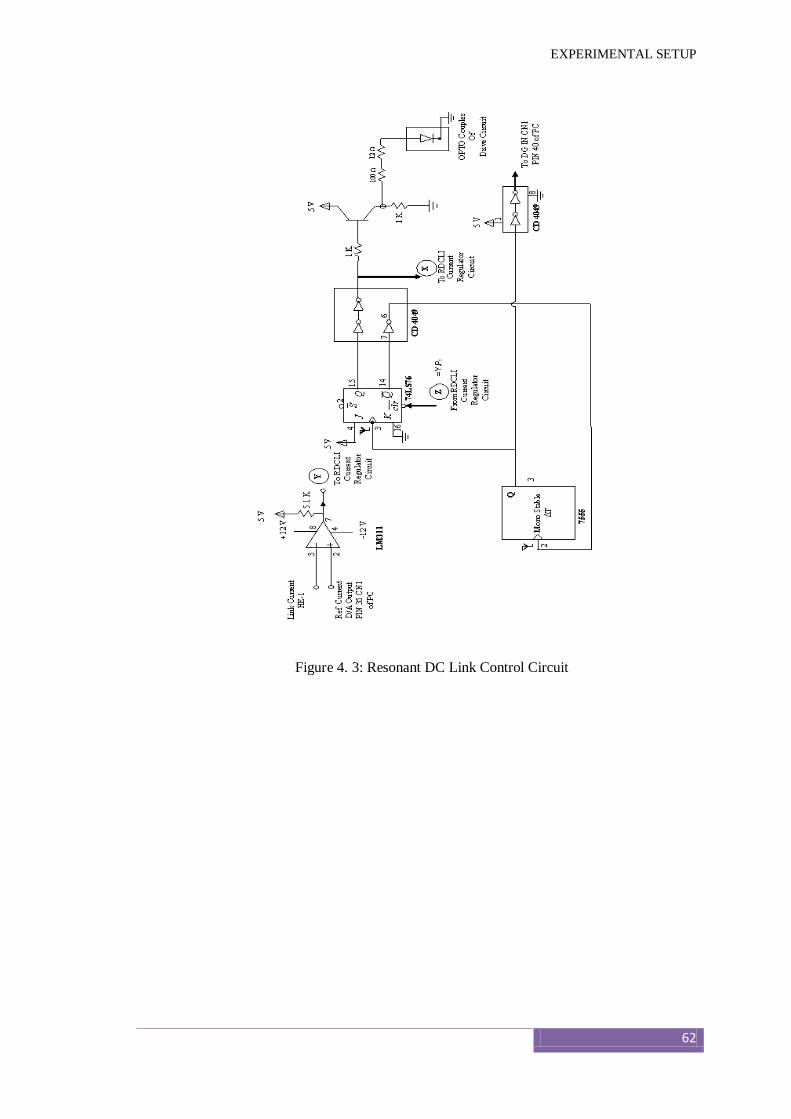
EXPERIMENTAL SETUP
62
Figure 4. 3: Resonant DC Link Control Circuit
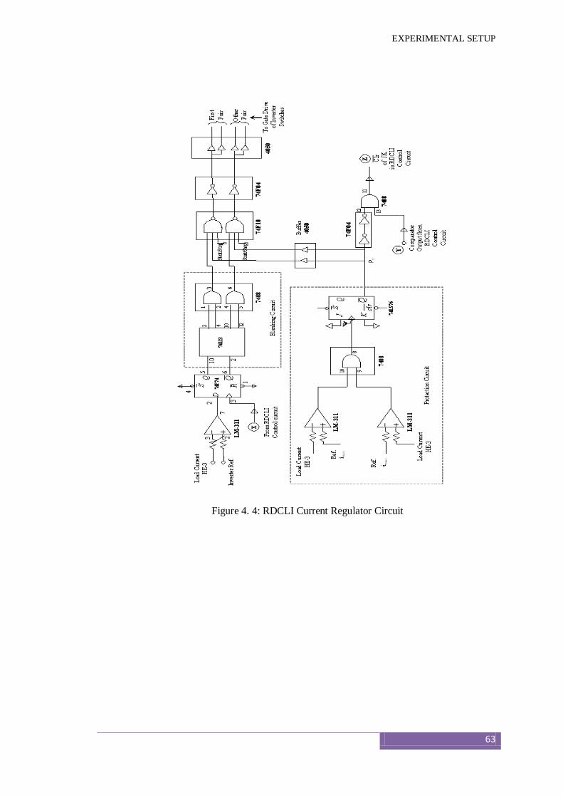
EXPERIMENTAL SETUP
63
Figure 4. 4: RDCLI Current Regulator Circuit
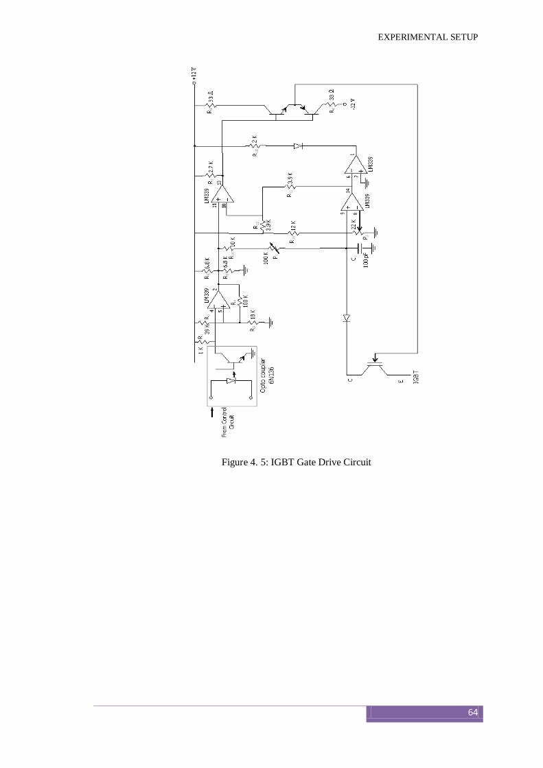
EXPERIMENTAL SETUP
64
Figure 4. 5: IGBT Gate Drive Circuit
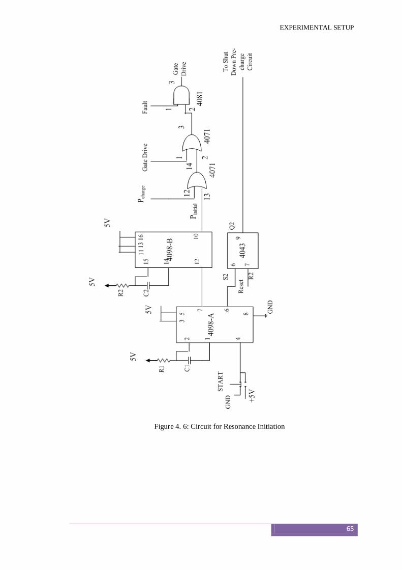
EXPERIMENTAL SETUP
65
Figure 4. 6: Circuit for Resonance Initiation
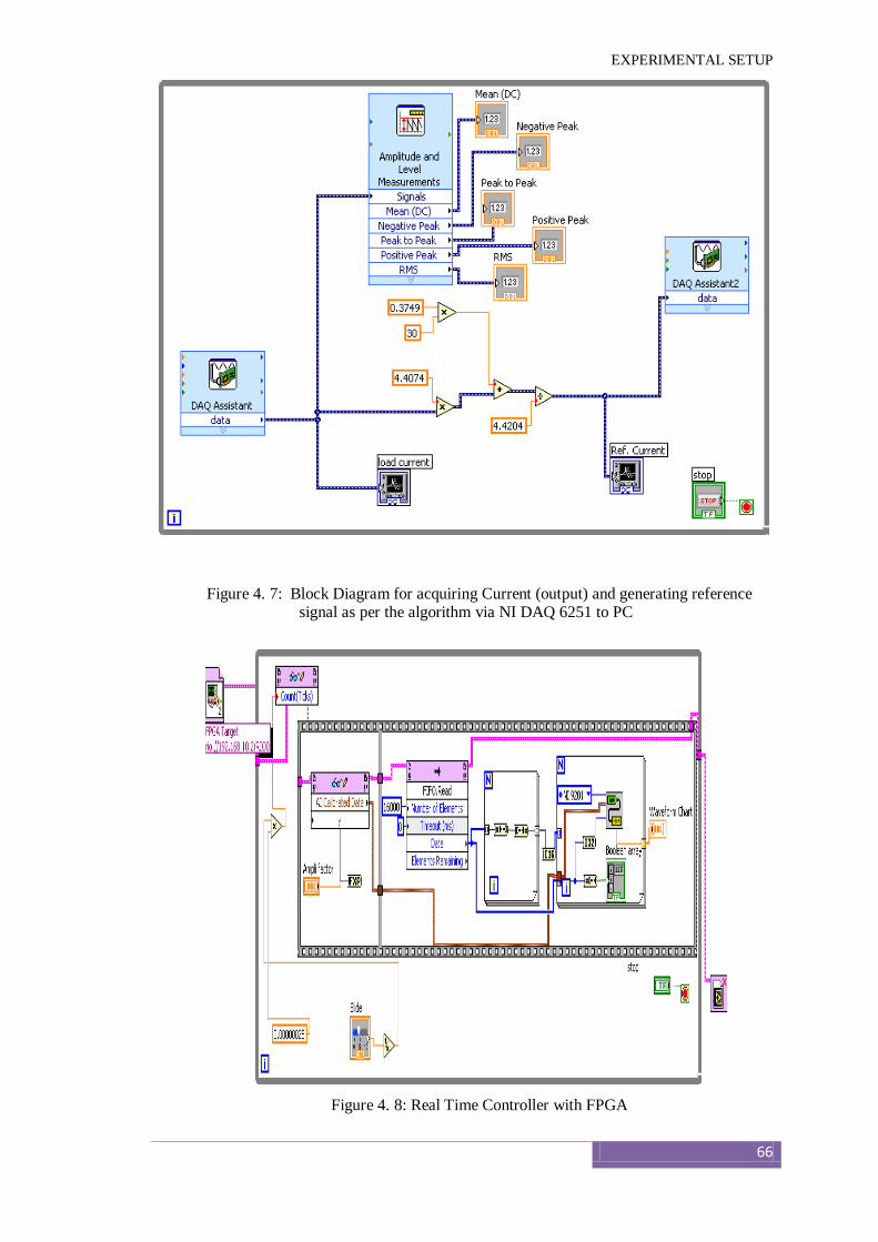
EXPERIMENTAL SETUP
66
Figure 4. 7: Block Diagram for acquiring Current (output) and generating reference signal as per the algorithm via NI DAQ 6251 to PC
Figure 4. 8: Real Time Controller with FPGA

EXPERIMENTAL SETUP
67
Figure 4. 9: Data Communication through ADC and DAC for Compact RIO
Figure 4. 10: Photograph Displaying DAQ Daughter board connected with PCI 6251,
Bridge Rectifier, RL Load
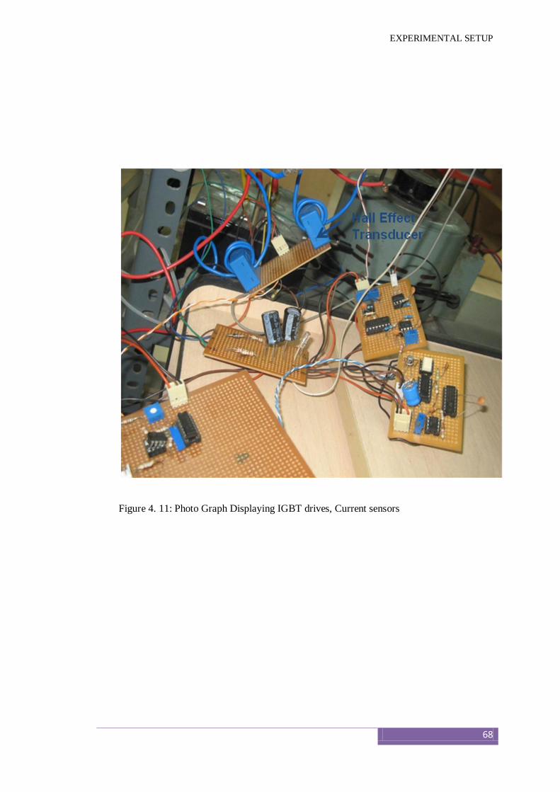
EXPERIMENTAL SETUP
68
Figure 4. 11: Photo Graph Displaying IGBT drives, Current sensors
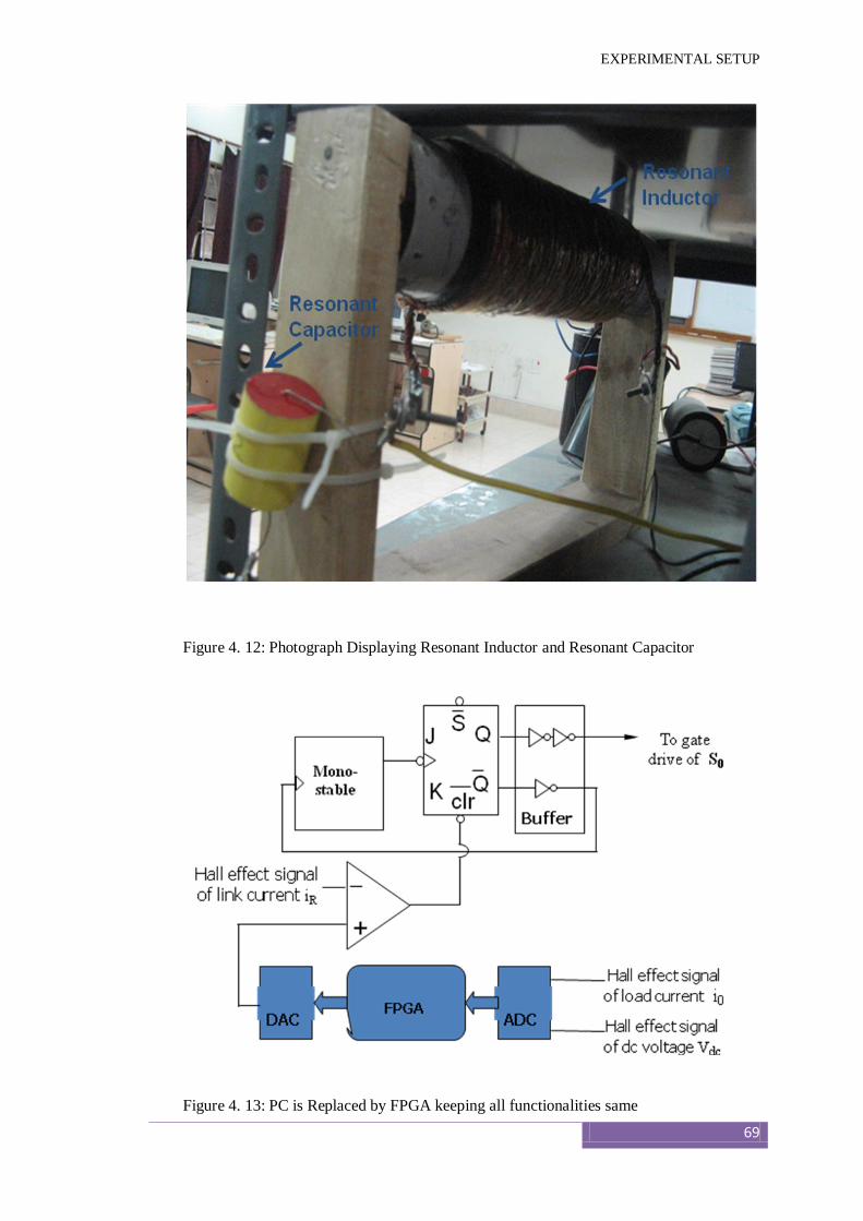
EXPERIMENTAL SETUP
69
Figure 4. 12: Photograph Displaying Resonant Inductor and Resonant Capacitor
Figure 4. 13: PC is Replaced by FPGA keeping all functionalities same
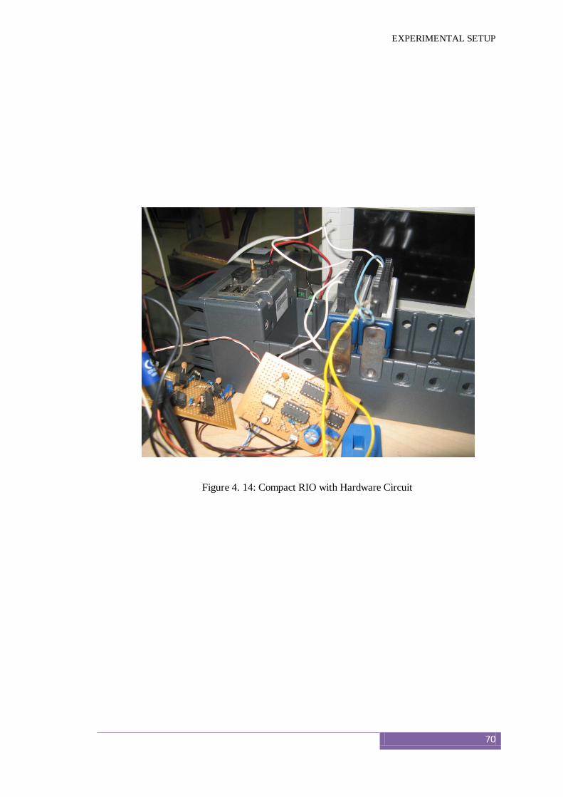
EXPERIMENTAL SETUP
70
Figure 4. 14: Compact RIO with Hardware Circuit

71
EXPERIMENTAL RESULTS
In this chapter the experimental results obtained in the laboratory are presented. For these
results we have considered single-phase RDCLI. The experiments are conducted at a lower
power level since the objective is to verify the principles already discussed in earlier chapters.
We start our discussions with the current initialization.
5.1 CURRENT INITIALIZATION
For the experimental set-up the resonant link parameters chosen are:
L = 33 H
C = 1 F
Q = 167
Vdc=30V(constant)
Chapter
5

EXPERIMENTAL RESULTS
72
With these values of inductor and capacitor the link frequency is 28 kHz and resonant time is
about 35.72 s. Therefore, time duration of 30.72 s is chosen as the resonant cycle time T
taking account of the finite Q-factor of the coil.
The block diagram of the current initialization scheme is shown in Figure 2.11. Through
this scheme, the zero-voltage switching (ZVS) is obtained. First, this ZVS property of the
inverter is tested with no load conditions ( 00i ). This is to test whether the link voltage goes to
zero after every 30.72 s.
The experimental results are shown in Figs. 5.1-5.6. In Figure 5.1, the link voltage, link
current and the gating signal of switch 0S are shown. The link voltage goes to zero after 30.72
s after the prescribed time ( T). The switch 0S is then turned on as is evident in Figure 5.1.
This switch remains in on state for time t so that the link current builds up to the desired level.
During this shorting interval, the link current increases linearly which can be seen from this
figure. The link current and the output of the monostable are shown in Figure 5.6. From this
figure it can be seen that the monostable goes low after about every 30.72 s and remains low in
that state till the comparator is activated. When the comparator output goes low, the monostable
is triggered. This remains high for 30.72 s after which it goes low. In the meanwhile the
comparator is reset. The required value of current for initialization is given to the comparator.
When the actual link current is equal to this value, comparator output goes low again and the
resonant cycle restarts. This is illustrated in Figure 5.6. Thus Figs. 5.2-5.6 clearly illustrate the
principle of working of the proposed current initialization for the RDLCI. Current initialization
at a constant load current (2 A) is shown in Figure 5.7. The constant current notion is only for the
resonant circuit as during the resonance time of 35 microseconds this sinusoidal load current
(400 Hz) is almost constant. The level to which the current should be initialized is changed
which is evident from the figure 5.1. In Figure 5. 7 we also show the inverter supplying a 400 Hz
load. This wave is almost a sinusoid except for some little chattering that is typically higher
order harmonics. It is also confirmed that the circuit is capable of sustaining a 400 Hz load and
the load waveform is also quite nice.
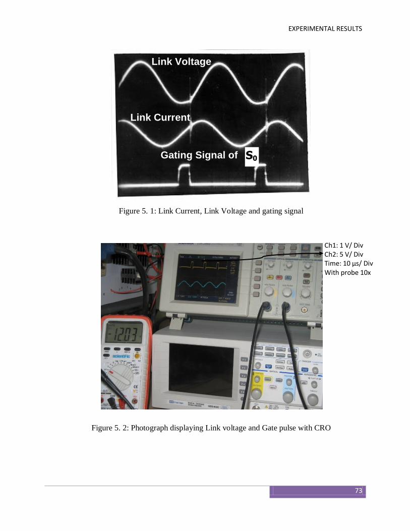
EXPERIMENTAL RESULTS
73
Link Current
Gating Signal of
Link Voltage
S0
Figure 5. 1: Link Current, Link Voltage and gating signal
Figure 5. 2: Photograph displaying Link voltage and Gate pulse with CRO
Ch1: 1 V/ Div Ch2: 5 V/ Div Time: 10 µs/ Div With probe 10x

EXPERIMENTAL RESULTS
74
Figure 5. 3: Photograph displaying link Voltage, and gate pulse in one CRO and Link current
in other CRO
Figure 5. 4: Link Voltage and Link current
Ch1: 1 V/ Div Ch2: 5 V/ Div Time: 10 µs/ Div With 10x probe
Ch1: 1 V/ Div Ch2: 5 V/ Div Time: 10 µs/ Div With 10x probe

EXPERIMENTAL RESULTS
75
Figure 5. 5: Gate Pulse and Link Current
Figure 5. 6: Comparator output and Monostable output
Ch1: 1 V/ Div Ch2: 5 V/ Div Time: 10 µs/ Div With 10x probe
Ch1: 1 V/ Div Ch2: 5 V/ Div Time: 10 µs/ Div With 10x probe
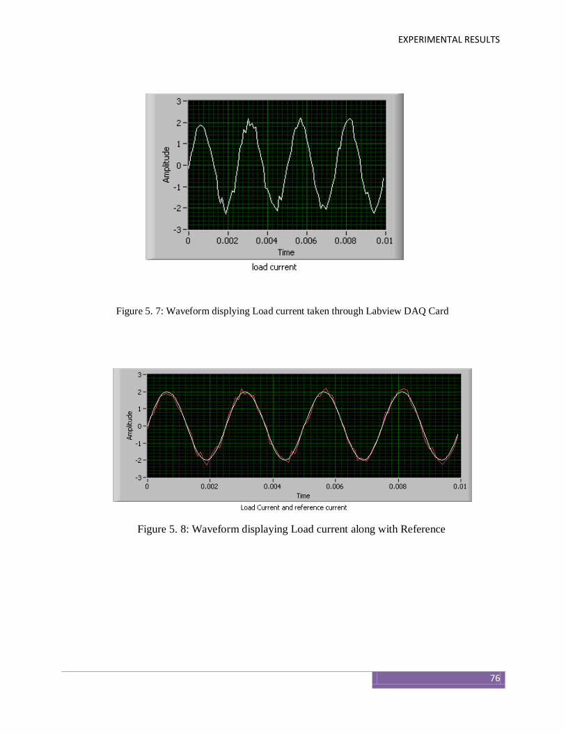
EXPERIMENTAL RESULTS
76
Figure 5. 8: Waveform displaying Load current along with Reference
Figure 5. 7: Waveform displying Load current taken through Labview DAQ Card

EXPERIMENTAL RESULTS
77
Figure 5. 9: Current waveform after connecting Compact RIO
5.2 CONCLUSIONS
The experimental results obtained from the lab prototypes are presented. The proposed
current initialization scheme for RDCLI based on state transition equation is experimentally
verified. It is shown that that this initial current prediction is quite accurate which in turn ensures
the zero crossing of the link voltage at a prescribed time instant. Zero crossing is achieved at
different load conditions. The proposed method is elegant and quite precise, yet simple to
implement. In addition it is also demonstrated experimentally that it is possible to supply a 400
Hz load.

78
CONCLUSIONS
The general conclusions drawn from this thesis and some suggested new directions
are presented in this chapter. The objective of this thesis is to determine a best-suited
topology for the power circuit for the Power Conditioning Unit (PCU) of the Variable
Speed Constant Frequency Aircraft Power supply (typically 400 Hz).
6.1 GENERAL CONCLUSIONS
The work done in this thesis to achieve the above-mentioned objectives is
summarized below.
1. Hard or Soft-switched inverter: The PWM techniques, to reduce sonorous pollution
and size of the transformer and output filter elements, need high switching
frequency (up to 20 kHz). In high switching frequency, the commutation losses are
high and they can be greater than conduction losses, resulting low efficiency. For a
Chapter
6
CONCLUSIONS
79
2. Hard-switched inverter, the increase in frequency will result in increased losses and
higher device stresses.
In a soft-switched inverter, the switchings are done when the voltage across the
switches is zero. Therefore, Ttheoretically there is no switching loss. A resonant dc
link inverter can be operated at a high frequency that is 5 to 10 times higher than
that of a hard-switched PWM inverter and can offer improved performance.
3. Current Initialization: In this thesis a new algorithm for current initialization scheme
is proposed for a resonant dc link inverter (RDCLI). The method of current
initialization is based on the state transition analysis of the system as a boundary
value problem (BVP). It is shown that for a given load current, it is possible force
the dc link voltage to go to zero at a prescribed time by properly choosing the initial
dc link current. This technique makes it possible to operate the resonant dc link
inverter without any zero-crossing failure, which is an important issue for a
satisfactory operation of such an inverter.
4. Power Loss Estimation: Detailed analysis of the losses in the resonant DC link
inverter is performed. Using the overall losses as a criterion, the design optimization
for the resonant DC link inverter intended for any industrial application yields an
optimal value of the resonant impedance. Loss calculations show that in the resonant
inverter the switching losses in the main devices are substantially reduced, and the
conduction losses become the major loss component. Under the identical expected
load conditions there is significant reduction in the switching losses in the main
devices and additionally there is reduction in total losses in comparison to the hard
switching counterpart operating at a switching frequency of 15 kHz.
5. 400 Hz Power Supply: In the AC-DC-AC conversion process a RDCLI is used as
the power circuit for supplying the 400 Hz load. The single-phase bridge inverter
after the resonant link uses zero-hysteresis bang-bang current control for controlling
current within the inverter and the switches in this inverter are switched at the
instant of zero voltage. The performance of the circuit while supporting a 400 Hz
load is evaluated through simulation and lab protye experiment. It is observed that

CONCLUSIONS
80
the circuit is capable of supplying the load the required waveform with a total
harmonic distortion of 2. 2%.
6. Implementation: PC interface is used for the implementation of the proposed current
initialization scheme. The use of a PC makes the system more flexible for
conducting experiments. This facilitates zero-voltage switching by taking into
account of the actual circuit delays and tolerances.
7. FPGA Implementation: Once we are satisfied with the performance of the circuit
behaviour and expected results, we replaced the PC with FPGA (NI CompactRIO);
with a futuristic hope that the control circuit will be replaced by FPGA/ ASIC
Implementation.
6.2 SCOPE FOR FUTURE WORK
Some suggested new directions of research in the area of 400 Hz power supply are
suggested in this section. These are
1. A soft-switch inverter topology with neutral point clamping needs to be
investigated.
2. A superior current control strategy than hysteresis control may be incorporated.
3. The control circuit can be fully converted to digital and hence will be great
candidate for FPGA exploration that would reduce the bulk of the circuit size
tremendously and an application specific integrated circuit(ASIC) can be developed.
81
BIBLIOGRAPHY
[1] J. D. Engelland, “The Evolving Revolutionary All-Electric Aeroplane.” IEEE
Transactions on Aerospace and Electronic Systems, Vol. AES-20, No. 2, March 1984,
pp.217-220.
[2] Claude Jacques, “The VSCF System Has Arrived.” NASA IAAA Joumal Article, Issue 05,
Revue Scientifiique et Technique, 3rd
Quarter, 1989, pp. 77-58.
[3] Quigley, R.E., March 1993, “More Electric Aircraft”, Proc. of 1993 IEEE Applied Power
Electronics Conf., San Diego, pp. 906-911.
[4] Weimer, J.A., October 1993, “Electrical Power Technology for the More Electric
Aircraft”, Proc. of IEEE 12th Digital Avionics Systems Conf., Fort Worth, pp. 445-450.
[5] Feiner, L.J., September 1994, “Power Electronics Transforms Aircraft Systems”, Proc. of
the WESCON94, Anaheim, pp. 166-171.
[6] Elbuluk, M.E. and Kankam, M.D., October 1996, “Potential Starter/Generator
Technologies for Future Aerospace Applications”, IEEE Aerospace and Electronics
Systems Magazine, vol. 11, no. 10, pp. 17-24.
[7] Eid, A. El-Kishky, H. Abdel-Salam, M. El-Mohandes, T. “Constant frequency aircraft
electric power systems with harmonic reduction,” Industrial Electronics, 2008. IECON
2008. 34th Annual Conference of IEEE, Nov. 2008, pp. 623-628.
[8] Lester Faleiro, "Beyond the more electric aircraft", AIAA, 2005.
[9] “Special Edition.” IEEE Transactions on Electronic Devices, Vol. 38 No. 7, July 1991.
[10] R. M. Duke and S. D. Round, "The steady state performance of a controlled current
Active Filter,” IEEE Transaction on Power Electronics, vol. 8, no.2, pp. 140-146, 1993.
[11] H. Akagi and Y. Kanazawa and A. Nabae, "Analysis and design of an active power filter
using quad-series voltage-source PWM converters," IEEE Transaction on Industry
Application, vol. 26, no.1, pp. 93-98, 1990.

82
[12] L. Moran, J. W. Dixon and R. R. Wallace, "A Three Phase Active Power Filter Operating
with Fixed Switching Frequency for Reactive Power and Current Harmonic
compensation," IEEE Trans on Industrial Electronics, vol. 42, no.4, pp. 402-408, 1995.
[13] G. Ledwich and P. Doulai, "Multipule Converter Performance and Active Filtering,
“IEEE Transaction on Power Electronics, vol. 10, no.3, pp. 273-279, 1995.
[14] P. Doulai and G.Ledwich, "Microcontroller-based strategy for reactive power control and
distortion compensation," IEE Proceedings, Vol. 137, no.6, pp. 364-372, 1990.
[15] L. K. Wong, Frank H. F. Leung, Peter K. S. Tam, “Control of PWM Inverter using a
Discrete-time Sliding Mode Controller,” IEEE 1999 International Conference on Power
Electronics and Drive Systems, PEDS'99, July 1999, Hong Kong.
[16] Salmon, J. Knight, A. Ewanchuk, J., “Single phase multi-level PWM Inverter
topologies using coupled inductors,” Power Electronics Specialists Conference, 2008.
PESC 2008. IEEE, pp. 802-808.
[17] B. Acharya and D. M. Divan and R. W. Gascoigne, "Active Power Filter using Resonant
Pole Inverter,” IEEE Transaction on Industry Application, vol.28,no.6, pp. 1269-1276,
1992.
[18] S. J. Finney, T. C. Green and B. W. Williams, “Review of resonant link topologies for
inverters,” ", IEE Proceedings, Pt.B., Vol. 140, no.2, pp. 103-114, 1993
[19] D. M. Divan, "The Resonant DC Link Converter -A New Concept in Static Power
Conversion,” IEEE Transaction on Industry Application, vol.25, no.2, pp. 317-325, 1989.
[20] D. M. Divan and G. Skibinski, "Zero Switching Loss Inverters for High Power
Applications," IEEE Transaction on Industry Application, vol. 25, no.4, pp. 634-643.,
1989.
[21] He and N. Mohan, W Wold “Zero Voltage Switching PWM Inverter for High Frequency
DC-AC Power Conversion” 1990 IEEE-IAS Annual Meeting Record, pp. 1215-1221.
[22] He and N. Mohan, “Parallel DC Link Circuit – A Novel Zero Switching loss Topology
with Minimum Voltage Stresses.” 1991 IEEE Transactions of Power Electronics, Vol. 6,
Number 4, pp.687-694.
[23] Venkataramanan and D. M. Divan, “Pulse width Modulation With Resonant DC Link
Converters” 1990 IEEE-IAS Annual Meeting Record, VOL.II, pp. 984-990.
83
[24] D. M. Divan and Giri Venkataramanan, “Comparative Evaluation of Switching Inverter
Topologies.” Proc. of the European Power Elctronics Conf., Vol. 2, pp. 13-18, 3-6 Sept.
1991.
[25] J. Flnney, T.C. Green, B. W. Williams, “Review of the Resonant Link Topologies for
Inverters.” IEE Proceedings-B, Vol. 140, No. 2, March 1993.
[26] K. K. Mahapatra. A. Ghosh and S. R. Doradla, “Improved active harmonic current
compensation of power electronic load using resonant dc link inverter,” The Journal of
Indian Institute of Science, vol. 77, pp. 585-595, Nov-Dec. 1997.
[27] K. K. Mahapatra. A. Ghosh and S. R. Doradla, “Active harmonic current compensation
of Industrial loads using resonant dc link inverter,” Proceedings of NPSC 96, pp-634-
639, Allied Publishers Limited, India, 1996.
[28] In-Hwan Oh, "The Zero-Voltage-Switching Parallel-Resonant DC Link (PRDCL)
Inverter with Minimized Conduction Loss,” IEEE Power Electronics Specialists
Conference (PESC'04), 35th Annual, Volume: 3, pp.1718-1723, 2004.
[29] W. S. Yu, J. S. Lai, S. Y. Park, “High Efficiency three phase soft-switching inverter for -
Electric vehicle drives”, IEEE Applied Power Electronics Conference, Feb 2009, pp.407-
412.
[30] M. Y. Wang, and K. Tian, “A nine switch three level inverter for electric vehicle
application,” IEEE Vehicle Power and Propulsion Conference, Sep 2008, pp 1-5.
[31] W. Gao, J. H. Zhang, X. F. Zhang, and J. H. Zhao, “ The analysis and experiment on full
soft-switching inverter under wide range input voltages,” IEEE Vehicle Power and
Propulsion Conference, Sep 2008, pp 1-8.
[32] W. Dong, J.Y. Choi, Y. Li, D. Boroyevich, F. C. Lee, and J.S. Lai, “Comparative
experimental evaluation of soft-switching inverter techniques for electric vehicle drive
applications,” IEEE Industry Applications Conf., Sep. 2001, pp. 1469-1476.
[33] G. Gong, M. Heldwein, U. Drofenik, J. Minibock, K. Mino and J. Kolar, "Comparative
evaluation of three-phase high-power-factor AC-DC converter concepts for application in
future more electric aircraft", IEEE Trans. Industrial Electronics, Vol. 52, No. 3, June
2005.
[34] DeDoncker ands J.P Lyons, "The Auxiliary ResonantCommutated Pole Converter,”1990
IEEE-IAS Conference Records, pp. 1228-1235.
[35] J. S. Lai and B. K. Bose, “An Improved Resonant DC Link Inverter for Induction Motor
Drives," Proceedings of Conf. Rec. IEEE/IAS Annual Meeting, pp. 742-748, 1988.

84
[36] J. S. Lai and B. K. Bose, "An Induction Motor Drive Using High Frequency Resonant
DC Link Inverter,",IEEE Transaction on Power Electronics, Vol. 6, no.3, pp. 504-513.,
1991.
[37] Vijay V. Deshpande, Seshagiri Rao Doradla and Deepakraj M. Divan, “ A Current-
Prediction Scheme for PRDCL Inverter-Fed Induction Motor Drive,” IEEE Transaction
on Power Electronics, Vol. 12, no.1, pp. 64-70., 1997.
[38] Jin He and Ned Mohan, “Parallel Resonant-DC Link Circuit - A Novel Zero Switching
Loss Topology with Minimum Voltage Stress," IEEE Transaction on Power Electronics,
vol. 6, no.4, pp. 687-694, 1991.
[39] M. H. Kheraluwala and D. M. Divan, "Delta Modulation Strategies for Resonant Link
Inverters,", IEEE Transaction on Industry Application, vol. 5, no.2, pp. 317-325, 1990.
[40] R. D. Lorenz and D. M. Divan, “ Dynamic analysis and experimental evaluation of delta
modulators for field oriented ac machine current regulators,” in Proc. 1987 IEEE/IAS
Annual Meeting, 1987, pp. 196-201.
[41] D. M. Divan, G. Venkataramanan and R. W. A. A. DeDoncker, “ Design methodologies
for soft switched inverters,” IEEE Transaction on Industry Application, vol. 29, no.1, pp.
126-135, 1993.
[42] E. W. Kimbark, Direct Current Transmission, New-York, Wiley Interscience, 1971
[43] Mukul Rastogi, Ned Mohan, Abdel-Aby Edris, “Hybrid active filtering of harmonic
currents,”IEEE Transaction on Power Delivery, vol. 10, no.4, pp. 1994-2000, 1995.
[44] Jou. H. L., Wu. J. C., Chu. H. Y., “New Single Phase Active Power Filter,” IEE
Proceedings, Electric Power Application, vol. 141, no. 3, pp. 129-134, May 1994.
[45] H. Akagi, Y. Kanazawa and A. Nabae, "Instantaneous Reactive Power Compensators
Comprising Switching Devices without Energy Storage Components,"IEEE Transaction
on Industry Application, vol. 20, no.3, pp. 625-630., 1984.
[46] G. W. White and TJE Miller, Soft-switching In Aircraft Power Conversion Systems
[47] Bellar, Wu T-Shiann, and A. Tchamdjou, “A review of Soft-Switched DC-AC
Converters,” IEEE Transactions on Industry Applications, Vol. 34, No. 4, Jyly 1998.
[48] H.Akagi, "New Trends in Active Filters for Power Conditioning," IEEE Transaction on
Industry Application, vol. 32, no. 6, pp. 1312-1322, Nov/Dec.1996.

85
[49] Grady, W. M. Samotyi, M. J. And Noyola, A. H., “Survey of active power line
conditioning methodologies,” IEEE Transaction on Power Delivery, vol. 5, no.3, pp.
1536-1542, 1990.
[50] Berringer Ken, (1995), "Semiconductor Power Loss in AC Inverter," in Conf. Rec. IEEE-
IAS Annu. Meeting, pp. 882-888.
[51] Clemente Steve, (1995), "A Simple Tool for the Selection of IGBTs for Motor Drives
and UPSs", in APEC'95 Rec, pp. 755-764.
[52] Kurnia Alexander, Cherradi Hassan, and Divan Deepakaj M., (1995), “Impact of IGBT
Behavior on Design Optimization of Soft Switching Inverter Topologies," IEEE Trans.
Ind. Applicat., vol. 31, pp. 280-286, March/April.
[53] Divan Deepakaj M. and Wallace Ian, (1997), “New Developments in Resonant DC Link
Inverters," in Conf. Rec. PCC'97-Nagaoka, pp.311-318.
[54] Mertens Axel and Divan Deepakaj M, (1990), " A High Frequency Resonant DC Link
Inverter Using IGBTs," in IPEC'90 Rec, pp. 152-160.
[55] Skibinski G. L. and Divan D. M., (1993a), “Design Methodology and Modeling of Low
Inductance Planar Bus Structure", in Rec. of Fifth European Conference on Power
Electronics and Application, pp.1029-1040.
[56] S. K. Pattnaik and K. K. Mahapatra “A Novel Control Circuit for Aircraft Power Supply
Using Soft-Switched Inverter” ICIT, pp.1-6, 2009 IEEE International Conference on
Industrial Technology, 2009.
[57] Schulting L., (1992), "A lOOkVA Resonant DC Link Inverter with GTOs- Design
Considerations and First Practical Experience," in Conf. Rec. IEEE-IAS Annu. Meeting,
pp. 29-736.
[58] K. Henny (ed), Radio Engineering Handbook, McGraw Hill Book Company, 1959
[59] Williams Mark Richard, 1993, “A Controlled Current Inverter for an Electric Vehicle”,
M. E. Thesis, University of Canterbury, Christchurch, New Zealand.
[60] Williams N., (1996), “Metalized Film Capacitor for High Frequency, High Current
Applications,” in IEE Colloquium on Capacitor and Inductor for Power Electronics, pp.
4/1-4/4.
[61] Mertens Axel and Divan Deepakaj M. (1990), “A High Frequency Resonant DC Link
Inverter Using IGBTs,” in IPEC’90 Rec., pp. 152-160.

86
APPENDIX A
DETAILS OF PC INTERFACE CARD
NI Data-Acquisition System
PCI-6251
Analog Input:
Number of channels: 8 differential or 16 single ended
ADC resolution: 16 bits
Sampling rate (Maximum): 1.25 MS/s single channel,
1.00 MS/s multi-channel (aggregate)
Timing accuracy: 50 ppm of sample rate
Timing resolution: 50 ns
Input coupling: DC
Input range: ±10 V, ±5 V, ±2 V, ±1 V, ±0.5 V, ±0.2 V, ±0.1 V
Maximum working voltage for analog inputs (signal + common mode): ±11 V of AI
GND
CMRR (DC to 60 Hz): 100 dB
Input impedance
Device on: AI+ to AI GND: >10 GΩ in parallel with 100 pF
AI- to AI GND: >10 GΩ in parallel with 100 pF
Device off: AI+ to AI GND: 820 Ω
AI- to AI GND: 820 Ω
Input bias current: ±100 pA
Crosstalk (at 100 kHz)
Adjacent channels: -75 dB
Non-adjacent channels: -90 dB
Small signal bandwidth (-3 dB): 1.7 MHz
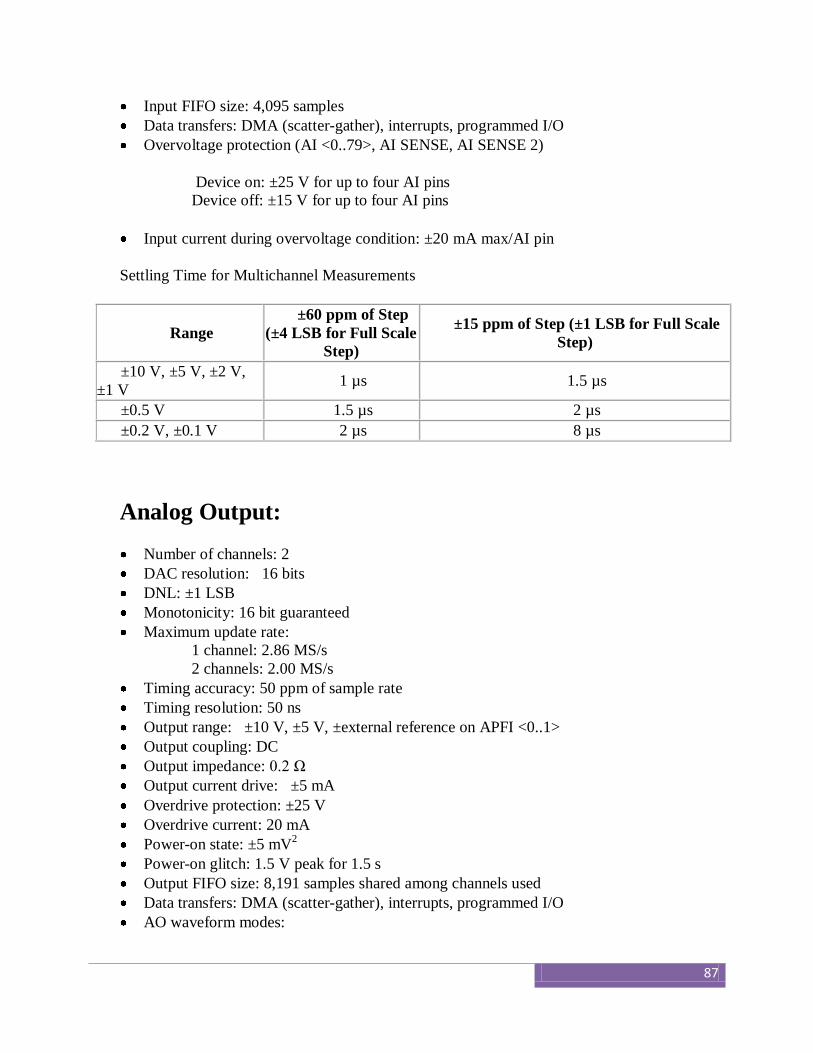
87
Input FIFO size: 4,095 samples
Data transfers: DMA (scatter-gather), interrupts, programmed I/O
Overvoltage protection (AI <0..79>, AI SENSE, AI SENSE 2)
Device on: ±25 V for up to four AI pins
Device off: ±15 V for up to four AI pins
Input current during overvoltage condition: ±20 mA max/AI pin
Settling Time for Multichannel Measurements
Range
±60 ppm of Step
(±4 LSB for Full Scale
Step)
±15 ppm of Step (±1 LSB for Full Scale
Step)
±10 V, ±5 V, ±2 V,
±1 V 1 µs 1.5 µs
±0.5 V 1.5 µs 2 µs
±0.2 V, ±0.1 V 2 µs 8 µs
Analog Output:
Number of channels: 2
DAC resolution: 16 bits
DNL: ±1 LSB
Monotonicity: 16 bit guaranteed
Maximum update rate:
1 channel: 2.86 MS/s
2 channels: 2.00 MS/s
Timing accuracy: 50 ppm of sample rate
Timing resolution: 50 ns
Output range: ±10 V, ±5 V, ±external reference on APFI <0..1>
Output coupling: DC
Output impedance: 0.2 Ω
Output current drive: ±5 mA
Overdrive protection: ±25 V
Overdrive current: 20 mA
Power-on state: ±5 mV2
Power-on glitch: 1.5 V peak for 1.5 s
Output FIFO size: 8,191 samples shared among channels used
Data transfers: DMA (scatter-gather), interrupts, programmed I/O
AO waveform modes:
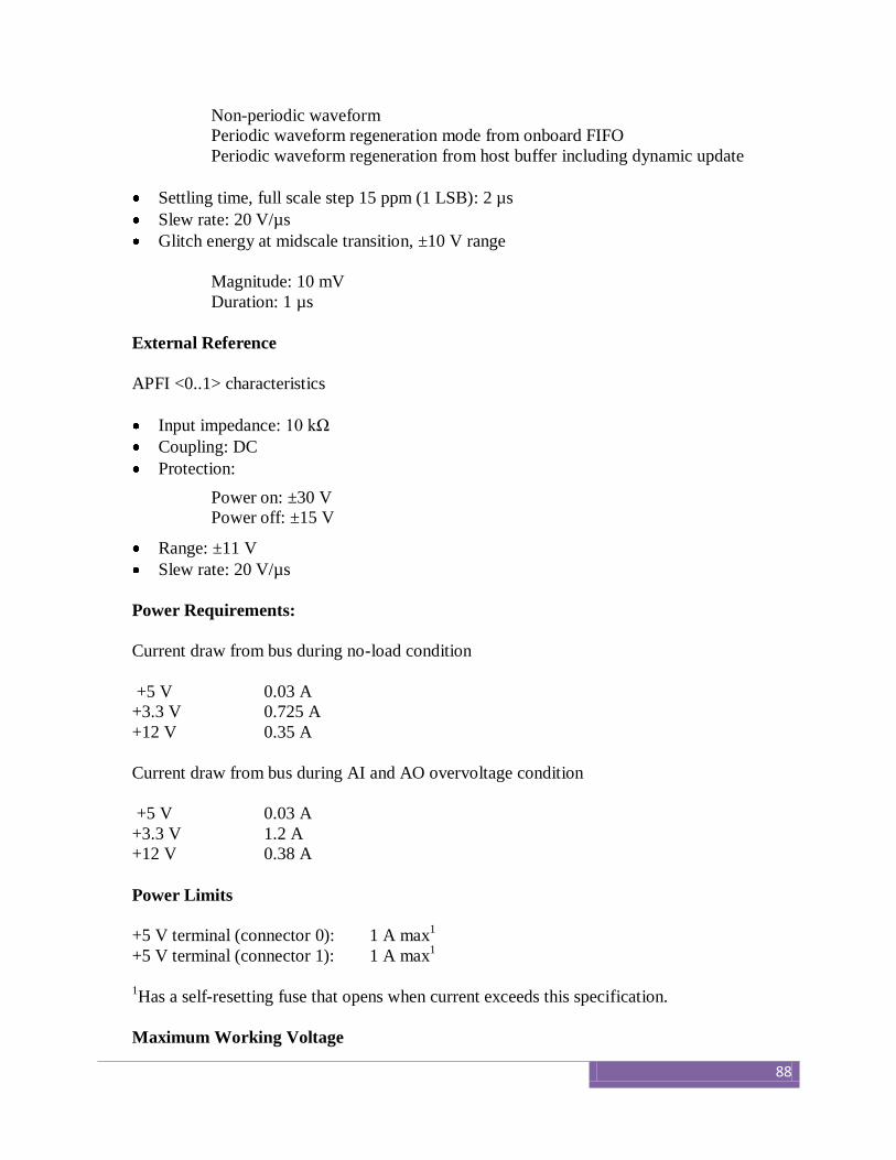
88
Non-periodic waveform
Periodic waveform regeneration mode from onboard FIFO
Periodic waveform regeneration from host buffer including dynamic update
Settling time, full scale step 15 ppm (1 LSB): 2 µs
Slew rate: 20 V/µs
Glitch energy at midscale transition, ±10 V range
Magnitude: 10 mV
Duration: 1 µs
External Reference
APFI <0..1> characteristics
Input impedance: 10 kΩ
Coupling: DC
Protection:
Power on: ±30 V
Power off: ±15 V
Range: ±11 V
Slew rate: 20 V/µs
Power Requirements:
Current draw from bus during no-load condition
+5 V 0.03 A
+3.3 V 0.725 A
+12 V 0.35 A
Current draw from bus during AI and AO overvoltage condition
+5 V 0.03 A
+3.3 V 1.2 A
+12 V 0.38 A
Power Limits
+5 V terminal (connector 0): 1 A max1
+5 V terminal (connector 1): 1 A max1
1Has a self-resetting fuse that opens when current exceeds this specification.
Maximum Working Voltage

89
11 V, Measurement Category I
(Maximum working voltage refers to the signal voltage plus the common-mode voltage.)
Environmental
Operating temperature: 0 to 55 °C
Storage temperature: -20 to 70 °C
Humidity: 10 to 90% RH, non-condensing
Maximum altitude: 2,000 m
Pollution Degree (indoor use only): 2
Reference: http://sine.ni.com/ds/app/doc/p/id/ds-22/lang/en#header12

90
APPENDIX B
DETAILS OF NI FPGA BASED EMBEDDED CONTROL
SYSTEM LAB HARDWARE
1. cRIO-9014 Real-Time PowerPC Controller for cRIO, 2 GB Storage Embedded controller runs LabVIEW Real-Time for deterministic control, data
logging, and analysis
400 MHz processor, 2 GB nonvolatile storage, 128 MB DRAM memory
10/100BASE-T Ethernet port with embedded Web and file servers with remote-
panel user interface
Full-speed USB host port for connection to USB flash and memory devices
RS232 serial port for connection to peripherals; dual 9 to 35 VDC supply inputs
-40 to 70 °C operating temperature range
Network
Network interface ................................... 10BaseT and 100BaseTX Ethernet
Compatibility .......................................... IEEE 802.3
Communication rates............................... 10 Mb/s, 100 Mb/s, auto-negotiated
Maximum cabling distance................. 100 m/segment
SMB Connector
Output Characteristics
Logic high............................................ 3.3 V
Logic low............................................. 0 V
Driver type........................................... CMOS
Sink/source current............................. ±50 mA
3-state output leakage current ........... ±5 μA
Input Characteristics
Minimum input level........................... -500 mV

91
Maximum input low level ................... 990 mV
Minimum input high level................... 2.31 V
Maximum input level .......................... 5.5 V
Input capacitance................................ 2.5 pF
Resistive strapping ............................. 1 kΩ to 3.3 V
USB Port
Maximum data rate ............................ 12 Mb/s
Maximum current................................ 500 mA
CompactRIO
Real-Time Controller Nonvolatile Storage DRAM
cRIO-9014 2 GB 128 MB
Memory
Use the following formula to determine the minimum life span in years of the
nonvolatile storage of your cRIO-901x controller:
Minimum life span in years = [Amount of memory in controller (MB) x
100,000 / 365 days] / [file size (MB) x write rate (per day)]
Power Requirements
Recommended power supply.............. 48 W secondary, 18 to 24 VDC
Power consumption
Controller only ................................ 6 W
Controller supplying power to eight CompactRIO modules........ 20 W
Power supply
On power-up ................................... 9 to 35 V
After power-up ............................... 6 to 35 V
2. cRIO-9104 8-slot 3 M Gate Reconfigurable Chassis for CompactRIO -40 to 70 °C operating range
Automatically synthesize custom control and signal processing circuitry using
LabVIEW
3M gate reconfigurable I/O (RIO) FPGA core for ultimate processing power
DIN-rail mounting options
8-slot reconfigurable embedded chassis accepts any CompactRIO I/O module
3. PS-5 Power Supply, 24 VDC, 5A, Universal Power Input Easy way to
distribute power from one power supply to up to 8 devices with
replaceable blade fuses.
92
4. NI 9201 8-Channel ±10 VDC, 500 kS/s, 12-bit Analog Input Module
8 analog inputs, ±10 V input range
500 kS/s aggregate sampling rate
12-bit resolution, single-ended inputs, screw terminal or D-Sub connectors
Hot-swappable operation; overvoltage protection; isolation
NIST-traceable calibration
-40 to 70 °C operating range
Signal Type: voltage
Channels: 8
Resolution (bits): 12
Max Sampling Rate (S/s): 500k
Signal Input Ranges: ±10 V
5. NI 9263 4-Channel +/-10 V, 100 kS/s per Channel, 16-Bit, Analog
Output Module
4 simultaneously updated analog outputs, 100 kS/s
16-bit resolution
Hot-swappable operation
NIST-traceable calibration
-40 to 70 °C operating range
Signal Type: voltage
Channels: 4
Resolution (bits): 16
Max Update Rate (S/s): 500k /ch
Signal Ranges: ±10 V
Current Drive: 1 mA/ch

DISSEMINATION OF THE RESEARCH WORK
1. S. K. Pattnaik, K. K. Mahapatra, “Aircraft Power Supply Design using Soft-switched
Inverter” Proceedings of National Conference on Computational Intelligence, Control
and Computer Vision in Robotics & Automation (CICCRA)-2008, NIT Rourkela.
2. S. K. Pattnaik, K. K. Mahapatra, “A Novel Control Strategy for 400 Hz Aircraft Power
Supply Using Resonant DC Link Inverter” Proceedings of National Conference on
Advances in Energy Conversion Technologies (AECT)-2008, MIT Manipal.
3. S. K. Pattnaik and K. K. Mahapatra “A Novel Control Circuit for Aircraft Power Supply
Using Soft-Switched Inverter” IEEE International Conference on Industrial Technology,
IEEE-ICIT-2009, Gippsland, Australia.
4. S. K. Pattnaik and K. K. Mahapatra “Power Loss Estimation for PWM and Soft-
switching Inverter using RDCLI”, International MultiConference of Engineers and
Computer Scientists- DATICS-IMECS’10, Hong Kong, 17-19 March, 2010.