DesignoftheFrontEndElectronicsfortheInfrared … · The microbolometer measures the cloud...
15
Design of the Front End Electronics for the Infrared Camera of JEM-EUSO, and manufacturing and verification of the prototype model Óscar Maroto a , Laura Díez-Merino a , Jordi Carbonell a , Albert Tomàs a , Marcos Reyes b , Enrique Joven b , Yolanda Martín b , J. A. Morales de los Ríos c , Luis Del Peral c and M. D. Rodríguez Frías c,b a SENER, C/ Creu Casas i Sicart, 86-88, Parc de l’Alba 08290 Cerdanyola del Vallès, Barcelona, Spain b Instituto de Astrofísica de Canarias (IAC), Vía Lactea s/n, Tenerife, Spain c SPace and AStroparticle Group (SPAS), UAH, Madrid, Spain January 27, 2015 Abstract The Japanese Experiment Module (JEM) Extreme Universe Space Observatory (EUSO) will be launched and attached to the Japanese module of the International Space Station (ISS). Its aim is to observe UV photon tracks produced by ultra-high energy cosmic rays developing in the atmosphere and producing extensive air showers. The key element of the instrument is a very wide-field, very fast, large-lense telescope that can detect extreme energy particles with energy above 10 19 eV. The Atmospheric Monitoring System (AMS), comprising, among others, the Infrared Camera (IRCAM), which is the Spanish contribu- tion, plays a fundamental role in the understanding of the atmospheric conditions in the Field of View (FoV) of the telescope. It is used to detect the temperature of clouds and to obtain the cloud coverage and cloud top altitude during the observation period of the JEM-EUSO main instrument. SENER is responsible for the preliminary design of the Front End Electronics (FEE) of the Infrared Camera, based on an uncooled microbolometer, and the manufacturing and verification of the prototype model. This paper describes the flight design drivers and key factors to achieve the target features, namely, detector biasing with electrical noise better than 100μV from 1 Hz to 10 MHz, temperature control of the microbolometer, from 10 ◦ C to 40 ◦ C with stability better than 10 mK over 4.8 hours, low noise high bandwidth amplifier adaptation of the microbolometer output to differential input before analog to digital conversion, housekeeping generation, microbolometer control, and image accumulation for noise reduction. It also shows the modifications implemented in the FEE prototype design to perform a trade- off of different technologies, such as the convenience of using linear or switched regulation for the temperature control, the possibility to check the camera performances when both microbolometer and analog electronics are moved further away from the power and digital electronics, and the addition of switching regulators to demonstrate the design is immune to the electrical noise the switching converters introduce. Finally, the results obtained during the verification phase are presented: FEE limitations, veri- fication results, including FEE noise for each channel and its equivalent NETD and microbolometer temperature stability achieved, technologies trade-off, lessons learnt, and design improvement to implement in future project phases. Keywords: JEM-EUSO, Front End Electronics, FEE, microbolometer, IRCAM, infra-red detec- tor. 1 arXiv:1501.06183v1 [astro-ph.IM] 25 Jan 2015
Transcript of DesignoftheFrontEndElectronicsfortheInfrared … · The microbolometer measures the cloud...

Design of the Front End Electronics for the InfraredCamera of JEM-EUSO, and manufacturing and
verification of the prototype model
Óscar Marotoa, Laura Díez-Merinoa, Jordi Carbonella, Albert Tomàsa, MarcosReyesb, Enrique Jovenb, Yolanda Martínb, J. A. Morales de los Ríosc,
Luis Del Peralc and M. D. Rodríguez Fríasc,b
aSENER, C/ Creu Casas i Sicart, 86-88, Parc de l’Alba 08290 Cerdanyola del Vallès, Barcelona, SpainbInstituto de Astrofísica de Canarias (IAC), Vía Lactea s/n, Tenerife, Spain
cSPace and AStroparticle Group (SPAS), UAH, Madrid, Spain
January 27, 2015
Abstract
The Japanese Experiment Module (JEM) Extreme Universe Space Observatory (EUSO) willbe launched and attached to the Japanese module of the International Space Station (ISS). Itsaim is to observe UV photon tracks produced by ultra-high energy cosmic rays developing in theatmosphere and producing extensive air showers.
The key element of the instrument is a very wide-field, very fast, large-lense telescope that candetect extreme energy particles with energy above 1019 eV. The Atmospheric Monitoring System(AMS), comprising, among others, the Infrared Camera (IRCAM), which is the Spanish contribu-tion, plays a fundamental role in the understanding of the atmospheric conditions in the Field ofView (FoV) of the telescope. It is used to detect the temperature of clouds and to obtain the cloudcoverage and cloud top altitude during the observation period of the JEM-EUSO main instrument.
SENER is responsible for the preliminary design of the Front End Electronics (FEE) of theInfrared Camera, based on an uncooled microbolometer, and the manufacturing and verification ofthe prototype model.
This paper describes the flight design drivers and key factors to achieve the target features,namely, detector biasing with electrical noise better than 100µV from 1 Hz to 10 MHz, temperaturecontrol of the microbolometer, from 10◦C to 40◦C with stability better than 10 mK over 4.8 hours,low noise high bandwidth amplifier adaptation of the microbolometer output to differential inputbefore analog to digital conversion, housekeeping generation, microbolometer control, and imageaccumulation for noise reduction.
It also shows the modifications implemented in the FEE prototype design to perform a trade-off of different technologies, such as the convenience of using linear or switched regulation for thetemperature control, the possibility to check the camera performances when both microbolometerand analog electronics are moved further away from the power and digital electronics, and theaddition of switching regulators to demonstrate the design is immune to the electrical noise theswitching converters introduce.
Finally, the results obtained during the verification phase are presented: FEE limitations, veri-fication results, including FEE noise for each channel and its equivalent NETD and microbolometertemperature stability achieved, technologies trade-off, lessons learnt, and design improvement toimplement in future project phases.
Keywords: JEM-EUSO, Front End Electronics, FEE, microbolometer, IRCAM, infra-red detec-tor.
1
arX
iv:1
501.
0618
3v1
[as
tro-
ph.I
M]
25
Jan
2015

1 Introduction
JEM-EUSO (Extreme Universe Space Observatory on the Japanese Experiment Module)[1], [2], [3] is anew type of observatory that will utilize very large volumes of the Earth’s atmosphere as a detector ofthe most energetic particles in the Universe. Its aim is to observe UV photon tracks produced by UltraHigh Energy Cosmic Rays (UHECR), with energy above 1019 eV, generating Extensive Air Showers(EAS) in the atmosphere. The Atmospheric Monitoring System (AMS)[4] plays a fundamental rolein our understanding of the atmospheric conditions in the Field of View (FoV) of the telescope andincludes an infra-red camera for cloud coverage and cloud top height detection.
The monitoring of the cloud coverage by JEM-EUSO with an Atmospheric Monitor System iscrucial to estimate the effective exposure with high accuracy and to increase the confidence level in theUHECRs events in particular at the threshold energy of the telescope. The AMS is a system used todetect the temperature of clouds and to obtain the cloud coverage and cloud top altitude during theobservation period of the JEM-EUSO main instrument. Cloud top height retrieval can be performedusing either stereo vision algorithms (therefore, two different views of the same scene are needed)or accurate radiometric information, since the measured radiance is basically related to the targettemperature and therefore, according to standard atmospheric models, to its altitude. The observedradiation is basically related to the target temperature and emissivity and, in this particular case,it can be used to get an estimate of the cloud heights. The AMS will comprise an Infrared Camera(IRCAM)[5],[6],[7],[8], a LIDAR and JEM-EUSO slow data.
IRCAM, the technological contribution of the Spanish Consortium, is able to detect infrared radia-tion of the target with emissivity (ε) greater than 0.6 and lower than 1 and estimates the temperatureof the target under investigation with accuracy better than 3 K. IRCAM consists of three subsystems:
• IRCAM Telecope Assembly.
• IRCAM Electronics Assembly.
• IRCAM Calibration Unit.
The main function of the IRCAM Telescope assembly is to acquire the infrared radiation and toconvert it into digital counts. For that purpose, the Telescope Assembly includes the IRCAM detector,an uncooled microbolometer, the dedicated electronics to control it, the Front End Electronics (FEE),and the optics.
The IRCAM Electronics Assembly provides mechanisms to process and transmit the images ob-tained by the FEE from the microbolometer. It is composed of the Instrument Control Unit (ICU)and the Power Supply Unit (PSU). Their main function is to control and manage the overall systembehavior, including the data management, the power drivers and the mechanisms.
Due to the requested accuracy measurement the IRCAM will perform an On-Board calibration bymeans of a dedicated Calibration Unit.
SENER is responsible for the preliminary design of the Front End Electronics (FEE) within theIRCAM, and the manufacturing and verification of the prototype model, under IAC supervision.
2 IRCAM FEE Main Requirements
The main requirements the IRCAM FEE shall comply with are listed in the following:
1. IRCAM FEE shall acquire images from an infrared detector, type ULIS UL 04 17 1, covering thespectral range 8− 14µm and measuring temperatures between 200 K and 320 K[9].
2. IRCAM FEE shall generate the bias needed by the infrared detector to operate. These areenlisted in Table 1.
3. The detector shall be controlled in temperature between 10◦ C and 40◦ C with stability betterthan 10 mK over 4.8 hours, by commanding the Thermo-Electric Cooler (TEC) of the mi-crobolometer.
2

Figure 1: IRCAM FEE block diagram
4. The NETD of the IRCAM FEE shall be lower than 75 mK @ 300 K and optics F#1 of the target.
5. IRCAM FEE shall be able to perform frame averaging of at least 4 consecutive frames.
6. FEE shall be able to perform operation of sum and subtracting of frames.
7. IRCAM FEE shall be composed of two different modules, each of them, located at differentpositions, joint by a flex cable:
• FPA Focal Plane assembly (detector + mechanical I/F to the Optical subsystem).
• FEE electronic box.
3 IRCAM FEE Flight Design Overview
IRCAM FEE has been divided into two different modules, namely, the Focal Plane Array (FPA)containing the low noise electronics needed for the infrared detector to operate optimally, and theFront End Electronics (FEE) hosting the digital electronics and TEC control circuitry.
Figure 1 shows the block diagram of the IRCAM FEE electronics.The main functionalities imple-mented in the IRCAM FEE are:
3.1 Power supplies generation for the FEE PCB
All the power supplies are cold redundant and consequently OR-ing is needed. This block also filtersthe input power supplies and generates secondary voltages by using linear regulators and point of loads.
3.2 TEC temperature control
The microbolometer performance is optimum when the detector is stabilized to a constant temperature±10 mK for the image acquisition time, presently defined as 4.8 h. To fulfil this requirement, the designshown in Figure 2 is featured in the IRCAM FEE.
This circuitry consists of a current regulator implemented with a buck converter and controlled by adouble loop. The possible setting temperatures are between 10 and 40◦C, and it is only possible to heatup due to the facts that the temperature of the FPA is expected to be lower than the microbolometersetting temperature, and in case of heating/cooling cycles were mixed during image acquisition, thethermal stability would be much worse than 10 mK.
3

Table 1: Requirements for microbolometer power supplies.
Electrical Bias Optimum Range Maximum Maximumfunction name Type value value current RMS noise
@ 300KVDDA Fixed 5 V 60 mA < 100µV(analog supply) ±100 mVVDDL Fixed 3.3 V 5 mA < 100 mV(digital supply) ±300 mVVBUS Fixed 2.8 V 1 mA < 100µV(microbolometerbiasing)
±25 mV
GFID Tunable Given 0 to 5V 1 mA 2µV (1Hz to 1kHz)(microbolometer in STR ±5 mV 5µV (1Hz to 10kHz)biasing) 100µV (1Hz to 10MHz)VSK (blind Tunable Given 2.0 to 5.5 V 1 mA 2µV (1 Hz to 1 kHz)microbolometer in STR ±5mV 5µV (1 Hz to 10 kHz)biasing) 100µV (1 Hz to 10 MHz)GSK (blind Fixed 2.2 V 1 mA 2µV (1 Hz to 1 kHz)microbolometer ±50 mV 5µV (1 Hz to 10 kHz)biasing) 100µV (1 Hz to 10 MHz)
Figure 2: TEC control block diagram.
The advantage of using a buck converter to implement the current regulator is the efficiency of thecircuit, and as the power availability is little, it has been decided to choose this option. The drawback isthat the switching noise could affect the low noise circuits as microbolometer power supplies generationor image acquisition. The alternative would be to use a linear regulator that is better in terms of noise,but the power consumption for big temperature jumps would be unaffordable. To analyze it, in theprototype the two options have been implemented to have a trade-off of both technologies.
3.3 Optical detector power supplies biasing
The required power supplies for the optical detector have very severe noise specifications and due tothis, most of the power supplies generators are located near the optical sensor.
The architecture of the optical detector power supplies generation is based on a voltage referencethat is adjusted and filtered by using very low noise operational amplifiers in non-inverting or invertingconfiguration. To filter the noise, a Sallen-key topology has been selected. The current driver onlyapplies to VDDA, which delivers 60 mA maximum, and consists of a bipolar transistor working in
4
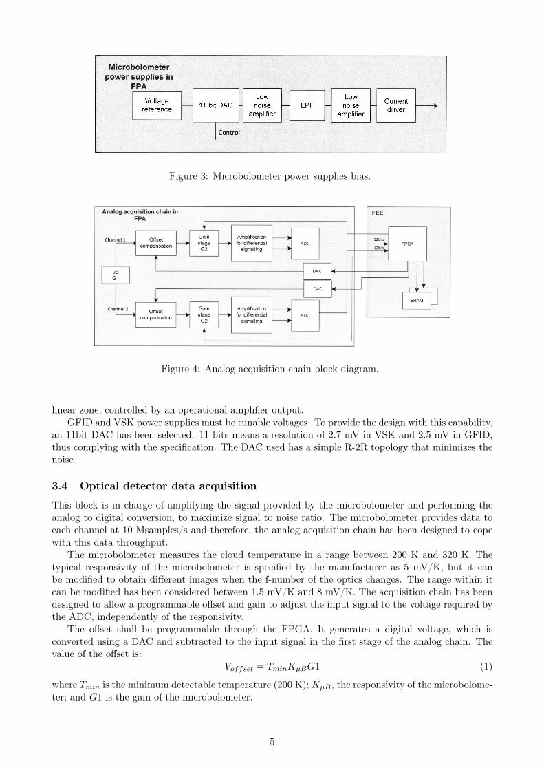
Figure 3: Microbolometer power supplies bias.
Figure 4: Analog acquisition chain block diagram.
linear zone, controlled by an operational amplifier output.GFID and VSK power supplies must be tunable voltages. To provide the design with this capability,
an 11bit DAC has been selected. 11 bits means a resolution of 2.7 mV in VSK and 2.5 mV in GFID,thus complying with the specification. The DAC used has a simple R-2R topology that minimizes thenoise.
3.4 Optical detector data acquisition
This block is in charge of amplifying the signal provided by the microbolometer and performing theanalog to digital conversion, to maximize signal to noise ratio. The microbolometer provides data toeach channel at 10 Msamples/s and therefore, the analog acquisition chain has been designed to copewith this data throughput.
The microbolometer measures the cloud temperature in a range between 200 K and 320 K. Thetypical responsivity of the microbolometer is specified by the manufacturer as 5 mV/K, but it canbe modified to obtain different images when the f-number of the optics changes. The range within itcan be modified has been considered between 1.5 mV/K and 8 mV/K. The acquisition chain has beendesigned to allow a programmable offset and gain to adjust the input signal to the voltage required bythe ADC, independently of the responsivity.
The offset shall be programmable through the FPGA. It generates a digital voltage, which isconverted using a DAC and subtracted to the input signal in the first stage of the analog chain. Thevalue of the offset is:
Voffset = TminKµBG1 (1)
where Tmin is the minimum detectable temperature (200 K);KµB, the responsivity of the microbolome-ter; and G1 is the gain of the microbolometer.
5

The whole gain of the analog chain is the product of the internal microbolometer gain (G1) andthe gain of the second stage of the chain (G2). The gain G1 is programmable via serial bus in theµB and the gain G2 is programmable via a resistance ladder multiplexed in the feedback loop. Theproduct G1 · G2 must amplify the voltage input signal to a 1Vpp differential signal (expected voltageat the ADC input), it is:
G1 ·G2 =Vin−ADCVmax−µB
=Vin−ADC
(Tmax − Tmin)KµB(2)
The possible values for G1 are specified by the manufacturer and the values for G2 have beencalculated to minimize the error in the amplification. These are detailed in Table 2. All combina-tions between G1 and G2 are allowed to adapt the chain gain to the adjustable responsivity of themicrobolometer. Minimum gain allowed shall be 1, while maximum gain for very low power signalscould rise up to 6.705.
Table 2: Programmable gain values in the analog acquisition chain
G1 G21.000 1.0001.125 1.0701.290 1.1401.500 1.2101.800 1.2802.250 1.3503.000 1.4204.500 1.490
Finally, after offset compensation and gain stage, the signal shall be converted from single-endedto differential signal before entering in the ADC.
The noise analysis performed for this module, which is the main contributor to the NETD addedby the FEE is depicted in Table 3.
Table 3: Analog acquisition chain noise for different responsivity values (microbolometer noise notincluded).
Responsivity Analog Chain Total Noise Equivalent NETD[mV/K] parameters [µV] [mK]K=1.50 G1=4.50 183.99 122.66
G2=1.21K=2.54 G1=3.00 179.95 70.85
G2=1.07K=3.71 G1=1.50 192.75 51.95
G2=1.49K=4.36 G1=1.29 190.39 43.67
G2=1.42K=5.22 G1=1.29 183.93 35.24
G2=1.21K=6.40 G1=1.29 178.09 27.82
G2=1.00K=7.30 G1=1.00 181.88 24.91
G2=1.14
Considering the microbolometer has a NETD around 60 mK for high responsibility values, the
6
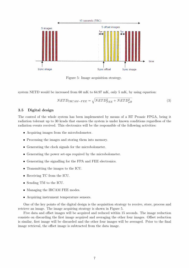
Figure 5: Image acquisition strategy.
system NETD would be increased from 60 mK to 64.97 mK, only 5 mK, by using equation:
NETDIRCAM−FEE =√NETD2
FEE +NETD2µB (3)
3.5 Digital design
The control of the whole system has been implemented by means of a RT Proasic FPGA, being itradiation tolerant up to 30 krads that ensures the system is under known conditions regardless of theradiation events received. This electronics will be the responsible of the following activities:
• Acquiring images from the microbolometer.
• Processing the images and storing them into memory.
• Generating the clock signals for the microbolometer.
• Generating the power set-ups required by the microbolometer.
• Generating the signalling for the FPA and FEE electronics.
• Transmitting the images to the ICU.
• Receiving TC from the ICU.
• Sending TM to the ICU.
• Managing the IRCAM FEE modes.
• Acquiring instrument temperature sensors.
One of the key points of the digital design is the acquisition strategy to receive, store, process andretrieve an image. The image acquiring strategy is shown in Figure 5.
Five data and offset images will be acquired and reduced within 15 seconds. The image reductionconsists on discarding the first image acquired and averaging the other four images. Offset reductionis similar, first image will be discarded and the other four images will be averaged. Prior to the finalimage retrieval, the offset image is subtracted from the data image.
7
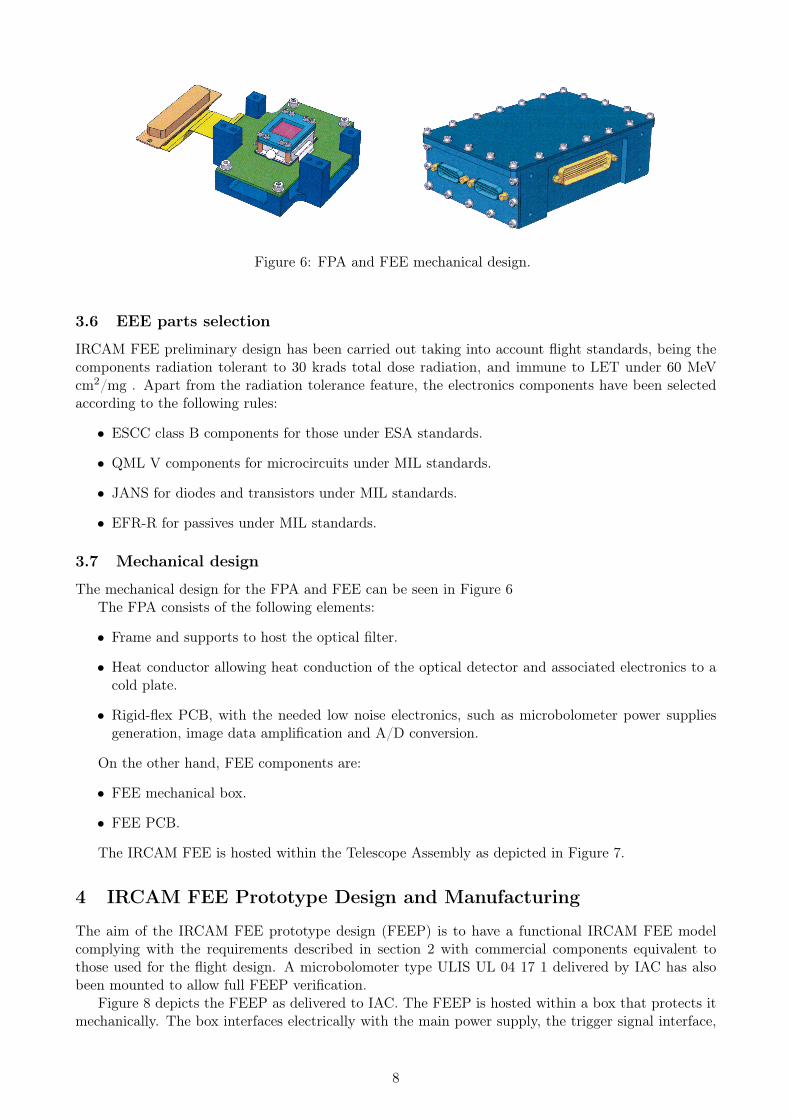
Figure 6: FPA and FEE mechanical design.
3.6 EEE parts selection
IRCAM FEE preliminary design has been carried out taking into account flight standards, being thecomponents radiation tolerant to 30 krads total dose radiation, and immune to LET under 60 MeVcm2/mg . Apart from the radiation tolerance feature, the electronics components have been selectedaccording to the following rules:
• ESCC class B components for those under ESA standards.
• QML V components for microcircuits under MIL standards.
• JANS for diodes and transistors under MIL standards.
• EFR-R for passives under MIL standards.
3.7 Mechanical design
The mechanical design for the FPA and FEE can be seen in Figure 6The FPA consists of the following elements:
• Frame and supports to host the optical filter.
• Heat conductor allowing heat conduction of the optical detector and associated electronics to acold plate.
• Rigid-flex PCB, with the needed low noise electronics, such as microbolometer power suppliesgeneration, image data amplification and A/D conversion.
On the other hand, FEE components are:
• FEE mechanical box.
• FEE PCB.
The IRCAM FEE is hosted within the Telescope Assembly as depicted in Figure 7.
4 IRCAM FEE Prototype Design and Manufacturing
The aim of the IRCAM FEE prototype design (FEEP) is to have a functional IRCAM FEE modelcomplying with the requirements described in section 2 with commercial components equivalent tothose used for the flight design. A microbolomoter type ULIS UL 04 17 1 delivered by IAC has alsobeen mounted to allow full FEEP verification.
Figure 8 depicts the FEEP as delivered to IAC. The FEEP is hosted within a box that protects itmechanically. The box interfaces electrically with the main power supply, the trigger signal interface,
8

Figure 7: IRCAM FEE location within Telescope Assembly.
Figure 8: IRCAM FEE prototype.
and the ICU simulation by means of three different connectors, and allows assembling of the optics ontop of the optical detector.
For practical purposes, it has been decided to have a single board in which the FPA and FEEsections electrically isolated, and potentially joined by a connector with a similar length as the flightflex connector. The FPA is located at the left half of the board, near the detector, while the FEE ishosted at the right half.
The detector is soldered on an independent assembly, being it possible to mount and dismountthe detector PCB from the rest of the electronics. The detector assembly will consist of the followingparts:
9
• Optical detector.
• Heat conductor.
• Optical detector PCB.
The heat conductor has been designed to have the same volume as the flight one, and is placed indirect contact with the detector base. A metallic braided strap leads the heat from the heat conductorto a cold point external to the FEEP. The PCB has two connectors to provide the detector assemblywith means to connect and disconnect it to/from the rest of the electronics.
In addition to the functional features of the flight design, the FEEP also has some other capabilitiesto ease the flight design testing and validation:
• The FEE and FPA side can be electrically communicated by two different ways, namely, a harnesssimulating the flex connector in the flight design, or directly by using electrical connections thatcan be enabled or disabled by means of jumpers located on the PCB. This way the effect of theharness length on the image results can be quantified.
• Apart from the buck converter designed for feeding the TEC, the prototype also features alinear regulator with the same purpose. The use of a linear regulator increases power needs butdecreases noise on power supplies, and therefore, a trade-off of the two technologies can be done.
• An external signal (3.3 V TTL or CMOS) allows triggering a single image acquisition.
• As already explained, the detector is mounted on an isolated assembly, and this might worsenNETD.
• A simulator of the temperature sensing within the optical detector is included to be able to testthe temperature regulation circuit with a standard Peltier.
• A single voltage supply of 24 V, 1 A is needed to feed the FEEP, and some DC/DC converters andlinear regulator generate internally the voltage required by the electronics to operate nominally.
5 IRCAM FEE Prototype Verification
The main results, limitations and lessons learned derived from the test campaign performed at SENERfacilities are presented in the next sections.
5.1 Microbolometer Power Supplies Noise
The measurement has been done only in the frequency range from 10 Hz to 51 kHz with a DynamicSignal Analyzer (DSA). Below 10 Hz the measurement instrument, i.e. spectrum analyser, introducesnoise one order of magnitude higher than the existing in the prototype board, and therefore, the lowerfrequency is limited to 10 Hz. The maximum frequency the DSA can measure is 51 kHz. A highpass filter with a cutting frequency of 1 Hz has been used to eliminate the continuous signal at zerofrequency.
The power spectral density (PSD) of the noise of each power supply is summarized in Table ??.The noise in low frequency is the bigger contribution to the final noise and it decreases as frequency
increases. To calculate the noise in the 10 MHz bandwidth, the noise has been considered white noiseand has been extrapolated, which is a worst case assumption. Using the spectral power distribution,the ratio between 10 MHz and 51 kHz is 14, which leads to the PSD values shown in Table 5.
All the values are compliant with the specifications with the exception of VDDA, which is slightlyhigher than specified. It could be due to the approximation done, which is a worst case considerationand in this case a measurement with higher bandwidth should be done.
10

Table 4: Power supplies noise PSD measurement.
Power Supply NoiseVSK@5V 4.90925 µVRMS
VGSK 4.98774 µVRMS
GFID@5V 5.0095 µVRMS
VDDA 8.5572 µVRMS
VDDL 20.0827 µVRMS
GND 4.91247 µVRMS
Table 5: Power supplies noise PSD extrapolation to 10 MHz.
Power Supply Noise Noise Microbolometer(10 Hz - 51 kHz) (10 Hz - 10 MHz) specification
VSK@5V 4.90925 µVRMS 68.743 µVRMS 100 µVVGSK 4.98774 µVRMS 69.842 µVRMS 100 µVGFID@5V 5.0095 µVRMS 70.147 µVRMS 100 µVVDDA 8.5572 µVRMS 119.824 µVRMS 100 µVVDDL 20.0827 µVRMS 281.214 µVRMS 100 µVGND 4.91247 µVRMS 68.788 µVRMS 100 µV
5.2 TEC long-term stability
In the preliminary design, a switching voltage regulator was chosen due to the better efficiency com-pared to the linear regulators. Nevertheless, the prototype has means to control the TEC in eithera switching or a linear way, just by shorting or opening some jumpers. One of the objectives of theFEEP fabrication is to decide which regulator configuration, switching or linear, is more suitable forJEM-EUSO needs. Our findings are the following:
• For small thermal jumps, it is, difference between ambient and TEC temperature less than 10K, the linear regulator configuration is recommended, as the power needed to operate is small(less than 200 mA at 3.3 V, it is, 0.66 W, for a 8◦C thermal jump), and the switching regulatorneeds a minimum thermal jump to operate achieving the 10 mK thermal stability requirement.Given the standard laboratory conditions in which the FEEP was tested, the linear regulatorconfiguration was used to perform the acceptance test, although the switching configuration hasalso been tested and its performance is considered correct.
• For big thermal jumps of more than 10◦C, both configurations are possible to be used, althoughthe linear configuration power consumption is bigger. In the tests performed at SENER in linearconfiguration, a thermal jump of 17 K implied an increase of 3.3 · 0.4 = 1.32 W in power.
Due to hardware constraints in the design, the maximum allowed current to the TEC is around 1.2A, and therefore the maximum thermal jump allowed for the linear configuration is around 40− 50K.Nevertheless, for such big thermal jumps, the switching configuration is strongly recommended.
Depending on the final design of JEM-EUSO, either the switching or linear configuration, or evena combination of both of them, can be used.
At SENER, two tests have been carried-out to measure the long-term stability of the microbolome-ter temperature over 4.8 hours, both in linear regulation configuration.
The first one with a temperature setting point of 30◦C while the ambient is at 22◦C showed amean temperature of 30.0023◦C and a standard deviation of 1.14 mK, much lower than the ±10 mKrequired.
11

Figure 9: Microbolometer temperature stability for 5th, Tamb = 22◦C, Tsensing = 30◦C.
Figure 10: Microbolometer temperature stability for 5 h, Tamb = 22◦C, Tsetting = 39◦C.
The second test was executed similarly, changing the setting point to 39◦C to have a 17◦C differencebetween ambient and the setting point. In this case, the mean is 38.9966◦C and the standard deviation2.70 mK, also within specifications.
5.3 Dead pixel effect
Due to the big changes in microbolometer output voltage level during image transmission and theabsolute maximum ratings for input voltage levels of the ADC, diodes have been added to protect theADC. The use of the diodes and its slow recovery time imply every time a dead pixel is read, the effectin the output image is two consecutive pixels in the same channel seen as dead pixels. Alternatives toprotect the ADC will be studied in further project phases.
5.4 NETD measurement without microbolometer
The noise of the whole acquisition chain, both analog and digital contribution of the IRCAM FEEprototype without the microbolometer has been measured. An offset on both channels of 0 V and aconfigurable input voltage generated by a voltage reference is used to acquire several complete images.
12

Figure 11: Dead pixel map and detail of the double dead-pixel effect.
Table 6 shows the input voltage, the digital mean value and standard deviation obtained (in ADCcounts and mK consideMicrobolomering a responsivity of 7.3 mV/K) in each channel after the ADCs.
Table 6: Noise measurement of the acquisition chains in the digital domain.
Input Voltage Channel 1 Channel 2[V] Mean NETD [ADC Mean NETD [ADC
[ADC counts] counts, mK] [ADC counts] counts, mK]0.1 381.77 0.95, 32 388.97 0.82, 270.2 799.21 0.94, 31 806.42 0.8, 270.3 1206.10 0.91, 30 1213.49 0.8, 270.4 1618.38 0.89, 30 1625.77 0.74, 250.5 2031.47 0.94, 30 2039.24 0.74, 250.6 2439.02 0.94, 31 2447.47 0.74, 250.7 2853.08 0.98, 33 2861.99 0.75, 250.8 3265.37 1.01, 34 3274.63 0.76, 250.9 3677.69 1.02, 34 3687.53 0.77, 260.99 4048.44 1.04, 35 4058.50 0.77, 26
According to Table 6, channel 1 is noisier than channel 2. This could be due to the PCB routing,although no direct cause has been found. Note the maximum NETD is 35 mK including also thereference voltage used to feed the FEEP, and therefore, this is a worst case NETD. Thus the worstcase IRCAM FEE NETD, considering the microbolometer has 60 mK NETD would be 69.46 mK,which is below the specified 75 mK. By using four images averaging, theoretically the NETD could bereduced by one half.
From Table 6 it can also be seen that channel 2 has 7 counts offset with respect to channel 1.This can be corrected by the FPGA as it has been characterized when a 0 V input is inserted in bothchannel 1 and 2.
Another main result is that the NETD does not depend on the use of linear or switching regulationfor the TEC control, so either regulator can be used in the final design.
These results can be complemented with the effects of the harness connecting FPA and FEE, whichhave not been evaluated so far. This is recommended to be done in the future to fully characterize theFEEP.
13

6 Conclusions
The IRCAM FEE preliminary design and prototype design, manufacturing and verification have beencarried out. The overall results show the FEEP NETD is within NETD budget even without frameaveraging.
The linear versus switching regulation options to control the microbolometer temperature havebeen studied. Accordingly, it is advisable to use linear regulation when the thermal jump betweenambient and microbolometer temperature is below 10◦C. Between 10◦C and 20◦C thermal jump, bothlinear and switching regulation options are possible, while above 20◦C the switching option is stronglyrecommended.
Although the overall results are considered successful, the effect of the harness connecting FPAand FEE on the IRCAM FEE NETD should be characterized in future studies, and an alternativeto the diodes protecting the channel acquisition ADCs causing the double dead pixel effect should beconsidered.
Acknowledgements
This work is funded by the Spanish Ministry of Economy and Competitiveness or MINisterio deEconomia y COmpetitividad (MINECO) under projects AYA-ESP 2011-29489-C03-01, AYA-ESP 2011-29489-C03-02, AYA-ESP 2012-39115-C03-01, AYA-ESP 2012-39115-C03-03, CSD2009-00064 (Con-solider MULTIDARK) and by Comunidad de Madrid (CAM) under project S2009/ESP-1496. Wewant to thank the JEM-EUSO collaboration, to which this work is entitled, and the Instituto deAstrofísica de Canarias (IAC) to give SENER the opportunity to join the JEM-EUSO project.
References
[1] Takahashi, Y. and the JEM-EUSO Collaboration, “The Jem-Euso Mission,” New J. Phys. 11(6),(2009).
[2] Ebisuzaki, T., Medina-Tanco, G. and Santangelo, A.,“The JEM-EUSO Mission,” Adv. Sp. Res.53(10), 1499–1505 (2014).
[3] J.H. Adams Jr. et al (JEM-EUSO Collaboration), “An evaluation of the exposure in nadir obser-vation of the JEM-EUSO mission,” Astroparticle Physics, 44, 76–90 (2013)
[4] Neronov, A., Rodriguez-Frias, M. D., Toscano, S. and Wada, S., “Atmospheric Monitoring Systemof JEM-EUSO,” Proc. 32nd Int.Cosm. Ray Conf., 91–94 (2011).
[5] Rodriguez-Frias, M. D., Licandro, J., Sabau, M. D., Reyes, M., Belenguer,T., Gonzalez-Alvarado,M.C., Joven, E., Morales de los Rios, J. A., Saez-Palomino, M., Prieto, Saez-Cano, G.,Carretero, J., Perez-Cano, S., del Peral, L., “Towards the preliminary Design Review of the InfraredCamera of the JEM-EUSO Collaboration” Proc. 33rd Int. Cosm. Ray Conf., 95–98, Rio de Janeiro(2013).
[6] Morales de los Rios, J. A., del Peral, L., Saez-Cano, G., Prieto, H., Carretero, J. H., Sabau, M. D.,Belenguer, T., Gonzalez Alvarado, C., Sanz Palomino, M. et al., “An End to End Simulation codefor the IR-Camera of the JEM-EUSO Space Observatory,” Proc. 33nd Int. Cosm. Ray Conf., Riode Janeiro (2013).
[7] The JEM-EUSO Collaboration, “The Infrared Camera onboard JEM-EUSO,” Experimental As-tron., (in press, 2014).
[8] Morales de los Ríos, J. A., et al, “The infrared camera prototype characterization for the JEM-EUSO space mission,” Nuclear Instruments and Methods in Physics Research, 74–83 (2014)
14

[9] ULIS, “Nano640E-UL 04 17 1-011,” 2014, in http://www.ulis-ir.com/index.php?infrared-detector=25–%m-640x480, (23 April 2014).
15