
DESIGNOFRECONFIGURABLEMULTIPLE...
15
Progress In Electromagnetics Research C, Vol. 6, 21–35, 2009 DESIGN OF RECONFIGURABLE MULTIPLE ELEMENTS MICROSTRIP RECTANGULAR LINEAR ARRAY ANTENNA M. T. Ali, M. R. Kamarudin, and T. A. Rahman Wireless Communication Center (WCC) Universiti Teknologi Malaysia 81310 UTM Skudai, Johor, Malaysia R. Sauleau Institut d’´ electronique et de t´ el´ ecommunications de Rennes i, (IETR) UMR CNRS 6164, University of Rennes 1, France M. N. Md Tan Wireless Communication Center (WCC) Universiti Teknologi Malaysia 81310 UTM Skudai, Johor, Malaysia Abstract—This paper presents a reconfigurable multiple element microstrip rectangular linear array antenna integrated with radio frequency (RF) switches. The corporate feed design concept is used to excite the linear array antenna that consists of 8 elements of rectangular patches at 5.8GHz. Two PIN diode switches were deployed at the feeding line to activate the two arrays of patches that are located on the left and right sides of the antenna structure. The behavior of the reconfigurable multiple element linear antenna array system has been investigated with respect to the beam shaping characteristic. The comparisons of the performance between two structures, with and without Wilkinson Power Divider (WPD) are discussed in this paper. Two different beam patterns were achieved through the reconfigurable antenna at different number of elements design that incorporates with PIN diode switches and modified WPD concept. The simulation and the measurement results for 4 and 8 elements array antenna structure are presented. Corresponding author: M. T. Ali ([email protected]).
Transcript of DESIGNOFRECONFIGURABLEMULTIPLE...

Progress In Electromagnetics Research C, Vol. 6, 21–35, 2009
DESIGN OF RECONFIGURABLE MULTIPLEELEMENTS MICROSTRIP RECTANGULAR LINEARARRAY ANTENNA
M. T. Ali, M. R. Kamarudin, and T. A. Rahman
Wireless Communication Center (WCC)Universiti Teknologi Malaysia81310 UTM Skudai, Johor, Malaysia
R. Sauleau
Institut d’electronique et de telecommunications de Rennes i, (IETR)UMR CNRS 6164, University of Rennes 1, France
M. N. Md Tan
Wireless Communication Center (WCC)Universiti Teknologi Malaysia81310 UTM Skudai, Johor, Malaysia
Abstract—This paper presents a reconfigurable multiple elementmicrostrip rectangular linear array antenna integrated with radiofrequency (RF) switches. The corporate feed design concept is usedto excite the linear array antenna that consists of 8 elements ofrectangular patches at 5.8 GHz. Two PIN diode switches were deployedat the feeding line to activate the two arrays of patches that are locatedon the left and right sides of the antenna structure. The behavior ofthe reconfigurable multiple element linear antenna array system hasbeen investigated with respect to the beam shaping characteristic.The comparisons of the performance between two structures, with andwithout Wilkinson Power Divider (WPD) are discussed in this paper.Two different beam patterns were achieved through the reconfigurableantenna at different number of elements design that incorporates withPIN diode switches and modified WPD concept. The simulation andthe measurement results for 4 and 8 elements array antenna structureare presented.
Corresponding author: M. T. Ali ([email protected]).
22 Ali et al.
1. INTRODUCTION
The reconfigurable antennas have drawn lots of attention in the wirelesscommunication systems recently. The demand for reconfigurableantenna has increased drastically since a decade. Reconfigurable beamshaping is an ideal for the detection of small and large targets atboth short and long ranges, including that the antenna is mountedon a high tower or hillside [1, 2]. Reconfigurable antennas are idealfor many military and mobile communication applications where it isrequired to have a single antenna that can be dynamically reconfiguredto transmit or receive on the same or multiple frequency bands [3–5]. It is advantageous to integrate beam shaping functionality intothe systems so one can vigorously vary the beam shapes in manyapplications such as airplane radar, protection from smart weaponsand point to point communication.
In [6, 7], the authors presented reconfigurable antennas, whichradiated at different beam pattern by adjusting the apertures andmaintaining their operating frequencies. The antenna presented in [3],described a dual band dipole antenna integrated with MEMS switches.However, this method typically used a dual operating frequencyto reconfigure the beam pattern. The antennas proposed in [8, 9]worked at dual operating frequencies with a reconfigurable radiationpattern. In the reconfigurable antenna, the structure of the antennacan be changed by integrating with the switches such as PIN diodeswitches [10], the field-effect transistor (FET) [11], the photo conductorswitches [12] or by electromechanical system (MEMS) switch [13–15],which were proposed a few years ago. By controlling the states of theswitches, to ON or OFF mode, several approaches were proposed forimplementing the reconfigurable antenna. Most of these approacheswere able to alter the fundamental characteristics of the antenna suchas operating frequency, bandwidth, polarization characteristics andradiation pattern [13].
Works presented in this paper describe and analyze thereconfigurable corporate feed microstrip patch antenna incorporatedwith PIN diode as an RF switch. The switching mechanism iscontrolled by the external DC voltage. Two switches are utilizedto realize the antenna with switchable beam shaping at frequency5.8 GHz. The antenna performances such as input return loss,bandwidth, half power beamwidth (HPBW), and radiation patternswere obtained.

Progress In Electromagnetics Research C, Vol. 6, 2009 23
2. ANTENNA DESIGN
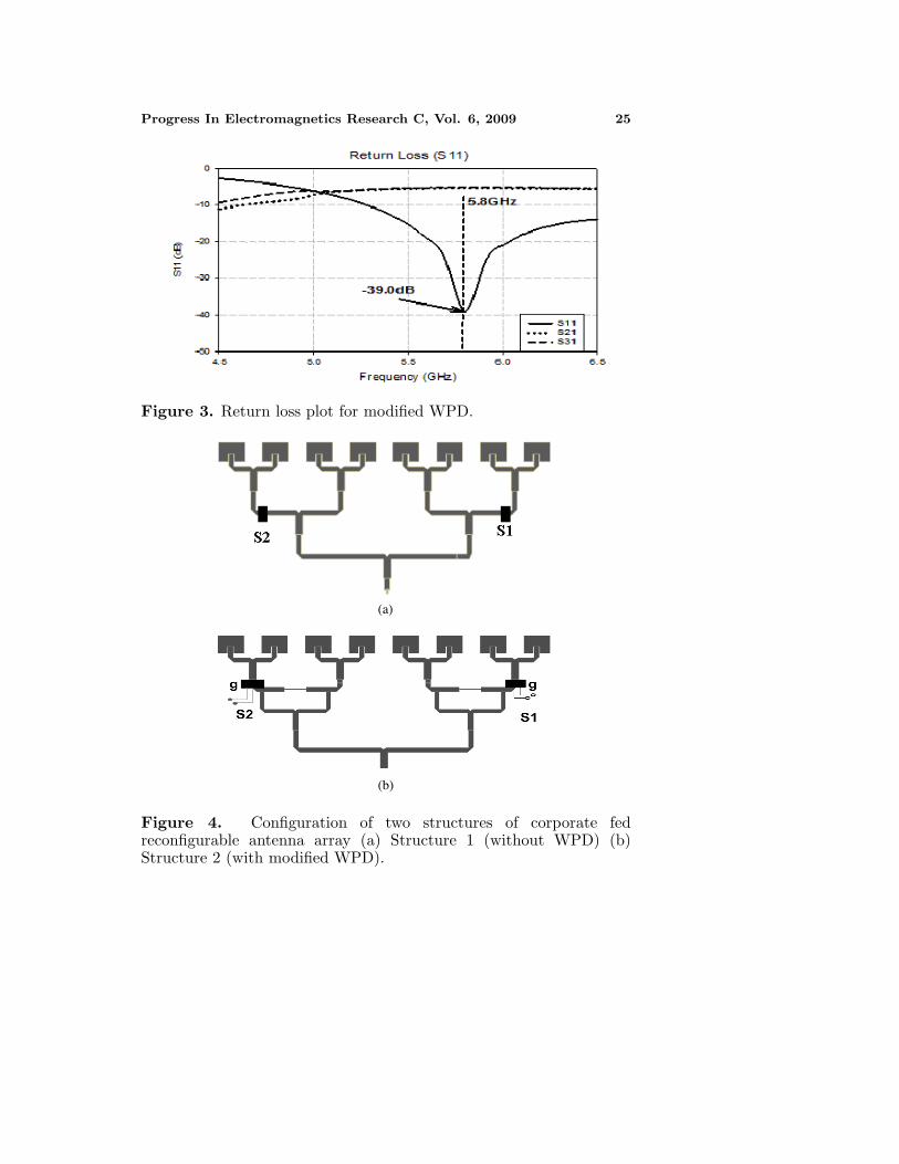
The configuration of the proposed reconfigurable antenna structuresis shown in Figure 4. There are two structures of reconfigurablemicrostrip patch antenna proposed in this design, without WPD asin structure 1 and added with modified WPD as in structure 2. Theantenna structure was constructed on FR-4 glass epoxy substrate whichhas a relative permittivity (εr) of 4.6 and loss tangent (δ) of 0.03; thethickness of the substrate is 1.6 mm.
(a) (b)
Figure 1. (a) Conventional Wilkinson power divider (b) the modifiedWilkinson power divider geometry.
Figure 2. Return loss due to length of 100 Ω transmission line.

24 Ali et al.
2.1. Power Divider Concept
The power divider is one of the most commonly used components in RFand microwave systems for power division and/or combination ratio asn-port network. The ideal design parameters are given in [8]. There aretwo common types of power divider used in an array antenna design,which are Wilkinson power divider and T-junction power divider.Figure 1 shows the structure of Wilkinson power divider. A lumpedresistor, 100 Ω (R), is connected between the outputs of two branchesand provides the required isolation. The dimensions of chip resistormust be very small, of the order of 1 × 0.5 mm. This implies thatthe two branches of the power divider must be placed very close toeach other to be connected to the resistor. This could produce strongmutual coupling between the output lines.
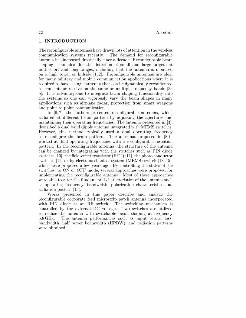
To overcome this problem, the 100 Ω chip resistor will be replacedby the λ/4 lengths of 100 Ω transmission line (S). A λ/4 length of 100 Ωtransmission line is placed in between λ/4 length of 50 Ω transmissionline (Z4 and Z5) as in Figure 1(b). The electrical performance of theWPD depends on the length of transmission line. These propertiesof modified WPD are illustrated in Table 1. In Figure 2, it can beseen that when the length of 100 Ω transmission line increases, theresonant frequency of the divider is shifted to the higher frequency,and the matching performance becomes worse. For these reasons, theproposed modified WPD is designed using 100 Ω transmission line witha length of 0.209λg. Figure 3 shows the performance of modified WPDwhich has good electrical characteristic with −39 dB of return loss at5.8 GHz.
Table 1. The properties of modified Wilkinson power divider.
Characteristics Z0 Z1 Z2 Z3 Z4 Z5
Impedance (Ω) 50 42.04 59.46 59.46 50 50Width (W), mm 2.92 3.65 2.239 2.239 2.92 2.92
A Wilkinson power divider with an arbitrary power ratio isexpressed as follows in Equation (1) to (7) [17].
P2
P3=
1K2
(1)
Z2 = Z0
√K (1 + K2) (2)
Z3 = Z0
√(1 + K2)
K3(3)
Progress In Electromagnetics Research C, Vol. 6, 2009 25
Figure 3. Return loss plot for modified WPD.
(a)
(b)
Figure 4. Configuration of two structures of corporate fedreconfigurable antenna array (a) Structure 1 (without WPD) (b)Structure 2 (with modified WPD).

26 Ali et al.
(a)
(b)
Figure 5. Comparison of return loss S11 (dB) between antennastructures 1 and 2 (a) 4 radiated elements (b) 8 radiated elements.
Z4 = Z0
√K (4)
Z5 =Z0√K
(5)
R = Z0 =
(1 + K2
)K
(6)
w = exp
[zc
(√εr + 1.41
)87
]0.8
5.98h(7)
Progress In Electromagnetics Research C, Vol. 6, 2009 27
(b)
(a)
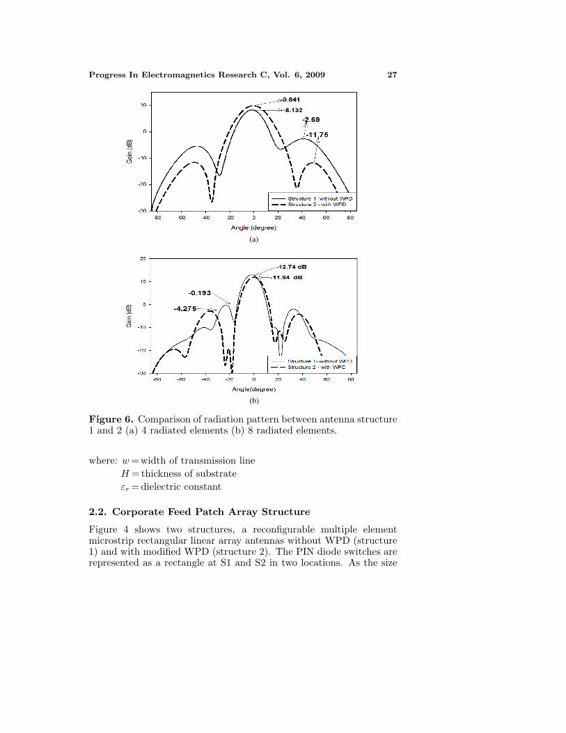
Figure 6. Comparison of radiation pattern between antenna structure1 and 2 (a) 4 radiated elements (b) 8 radiated elements.
where: w = width of transmission lineH = thickness of substrateεr = dielectric constant
2.2. Corporate Feed Patch Array Structure
Figure 4 shows two structures, a reconfigurable multiple elementmicrostrip rectangular linear array antennas without WPD (structure1) and with modified WPD (structure 2). The PIN diode switches arerepresented as a rectangle at S1 and S2 in two locations. As the size

28 Ali et al.
Table 2. The summary of simulation results obtained for thereconfigurable linear array antenna for both structures.
AntennaReturn loss S11(dB) Gain (dB) Sidelobe Ratio (dB)
ON OFF ON OFF ON OFF
Structure 1 −16.56 −24.49 12.74 8.13 12.93 10.82
Structure 2 −23.56 −29.61 11.94 9.84 16.22 21.6
Figure 7. Schematic representation of the switching circuitcomponents inserted in active feeding network.
of the switch is 2.5 × 1.4 mm, the gap (g) between the transmissionlines is designated as 0.5 mm. In this method, a DC bias circuit isused to control the ON/OFF mode of PIN diode switches. The beamwidth can be varied by altering the number of array elements. Whenall the diodes are switched ON, this antenna basically operates at aconcave pattern of 5.8 GHz. In contrast, when they are turned OFF,the antenna element is reduced to four elements with a convex pattern
Progress In Electromagnetics Research C, Vol. 6, 2009 29
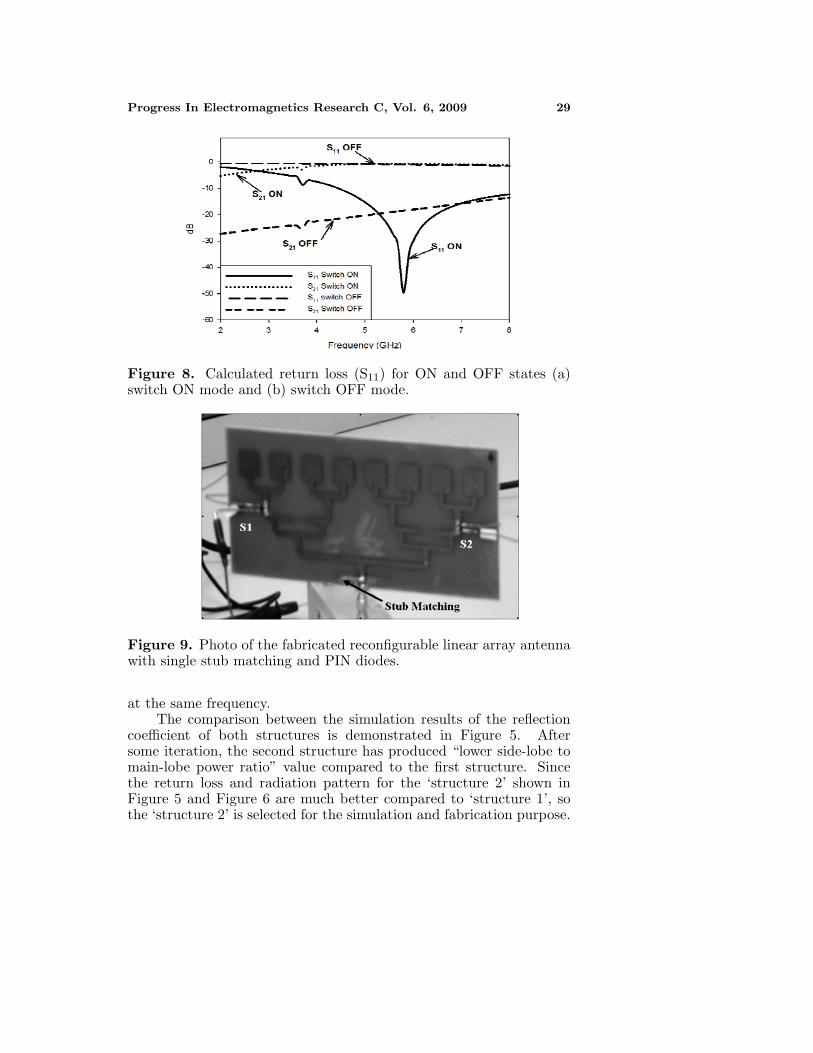
Figure 8. Calculated return loss (S11) for ON and OFF states (a)switch ON mode and (b) switch OFF mode.
Figure 9. Photo of the fabricated reconfigurable linear array antennawith single stub matching and PIN diodes.
at the same frequency.The comparison between the simulation results of the reflection
coefficient of both structures is demonstrated in Figure 5. Aftersome iteration, the second structure has produced “lower side-lobe tomain-lobe power ratio” value compared to the first structure. Sincethe return loss and radiation pattern for the ‘structure 2’ shown inFigure 5 and Figure 6 are much better compared to ‘structure 1’, sothe ‘structure 2’ is selected for the simulation and fabrication purpose.
30 Ali et al.
(b)
(a)
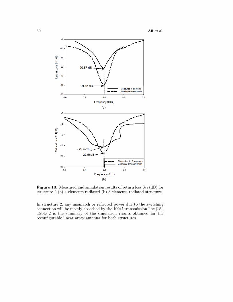
Figure 10. Measured and simulation results of return loss S11 (dB) forstructure 2 (a) 4 elements radiated (b) 8 elements radiated structure.
In structure 2, any mismatch or reflected power due to the switchingconnection will be mostly absorbed by the 100 Ω transmission line [18].Table 2 is the summary of the simulation results obtained for thereconfigurable linear array antenna for both structures.

Progress In Electromagnetics Research C, Vol. 6, 2009 31
Figure 11. Measured results of S11 when switch on/off state.
2.3. PIN Diode RF Switching Circuit
Philips PIN diodes, BAP51-02 [16] have been selected in this design.Figure 7 shows the schematic diagram of the switching circuit. Itcan be seen that the switch is inserted in between two transmissionlines. Each switching circuit consists of a PIN diode, two DC blockcapacitors, two inductors and one resistor. The capacitors, (C1-C2),are used as DC blocking and the inductors, (L1-L2), are used as RFchokes which provide low impedance for DC. The biasing voltage (6 V)has been connected to 100 Ω resistor to limit the current flow to theswitch. The simulation results using the PIN diode’s equivalent circuitsfor the OFF and ON-stages are presented in Figure 8. The return lossis less than −40 dB for the ON stage and an approximate of 0 dB forthe OFF stage at 5.8 GHz. The selected capacitance and inductancevalues were chosen to be 6.8 pF and 22 nH, respectively.
3. EXPERIMENTAL RESULT
The antenna with modified WPD (structure 2) described in Section 2has been fabricated and tested. The prototype of the antenna is shownin Figure 9. To tune the frequency of the antenna to have betterimpedance matching, a single open stub is necessary. Therefore, asingle quarter-wavelength open stub, which operates at 5.8 GHz, isadded to microstrip feeding line as shown in Figure 9. According to thesimulation results, the radiation pattern characteristic of the antennaforming has been tuned efficiently, since its structure is symmetricalby the center. The pattern obtained is directed to zero degree.

32 Ali et al.
(b)
(a)
Figure 12. Simulation and measured results of normalized radiationpattern for 4 and 8 element structures.
The radiation pattern of the 4 and 8 elements structure are shownin Figure 12(a) with 3 dB half power beamwidth (HPBW) of 22and 12.6, respectively. Meanwhile the simulated return loss for thetwo structure are −29.43 dB and −23.56 dB, respectively as shown inFigure 10. Referring to Figure 12, it is clearly shown that when thenumbers of the elements are increased, the beamwidth becomes narrowwith lower sidelobe and higher magnitude.
Measurements of reconfigurable beam shaping antenna was alsoconducted. The measured return loss compared with the simulated
Progress In Electromagnetics Research C, Vol. 6, 2009 33
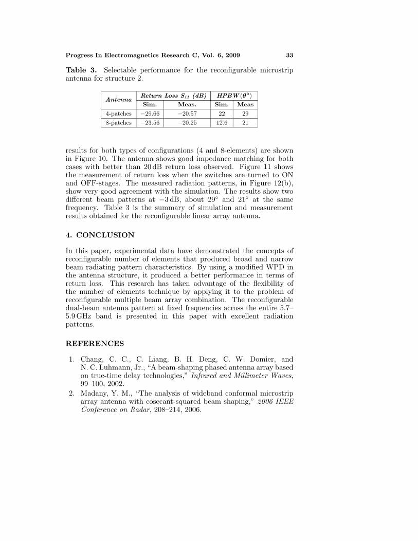
Table 3. Selectable performance for the reconfigurable microstripantenna for structure 2.
AntennaReturn Loss S11 (dB) HPBW (θ)
Sim. Meas. Sim. Meas
4-patches −29.66 −20.57 22 29
8-patches −23.56 −20.25 12.6 21
results for both types of configurations (4 and 8-elements) are shownin Figure 10. The antenna shows good impedance matching for bothcases with better than 20 dB return loss observed. Figure 11 showsthe measurement of return loss when the switches are turned to ONand OFF-stages. The measured radiation patterns, in Figure 12(b),show very good agreement with the simulation. The results show twodifferent beam patterns at −3 dB, about 29 and 21 at the samefrequency. Table 3 is the summary of simulation and measurementresults obtained for the reconfigurable linear array antenna.
4. CONCLUSION
In this paper, experimental data have demonstrated the concepts ofreconfigurable number of elements that produced broad and narrowbeam radiating pattern characteristics. By using a modified WPD inthe antenna structure, it produced a better performance in terms ofreturn loss. This research has taken advantage of the flexibility ofthe number of elements technique by applying it to the problem ofreconfigurable multiple beam array combination. The reconfigurabledual-beam antenna pattern at fixed frequencies across the entire 5.7–5.9 GHz band is presented in this paper with excellent radiationpatterns.
REFERENCES
1. Chang, C. C., C. Liang, B. H. Deng, C. W. Domier, andN. C. Luhmann, Jr., “A beam-shaping phased antenna array basedon true-time delay technologies,” Infrared and Millimeter Waves,99–100, 2002.
2. Madany, Y. M., “The analysis of wideband conformal microstriparray antenna with cosecant-squared beam shaping,” 2006 IEEEConference on Radar, 208–214, 2006.

34 Ali et al.
3. Kiriazi, J., H. Ghali, H. Ragaie, and H. Haddara, “Reconfigurabledual-band dipole antenna on silicon using series MEMS switches,”Antennas and Propagation Society International Symposium,Vol. 1, 403–406, 2003.
4. Mak, A. C. K., C. R. Rowell, R. D. Murch, and C. L. Mak, “Re-configurable multiband antenna designs for wireless communica-tion devices,” IEEE Transactions on Antennas and Propagation,1919–1928, Vol. 55, 2007.
5. Christodoulou, C. G., D. Anagnostou, and V. Zachou, “Leadinvited talk: Reconfigurable multifunctional antennas,” IEEE,176–179, 2006.
6. Simons, R. N., “Novel on-wafer radiation pattern measurementtechnique for MEMS actuator based reconfigurable patchantennas,” Technical Report, 24th Annual Antenna MeasurementTechniques Association Meeting and Symposium, NASA/TM—2002-211816 NASA, Glenn Research Center, Cleveland, Ohio,2002.
7. Pringle, L. N., P. G. Friederich, S. P. Blalock, G. N. Kiesel,P. H. Harms, D. R. Denison, E. J. Kuster, T. L. Fountain,and G. S. Smith, “GTRI reconfigurable aperture design,” IEEETransactions on Antennas and Propagation, Vol. 1, 473–476, 2002.
8. Yang, F., X.-X. Zhang, X. Ye, and Y. Rahmat-Samii, “Wide-bandE-shaped patch antennas for wireless communications,” IEEETransactions on Antennas and Propagation, Vol. 49, 1094–1100,2001.
9. Peroulis, D., K. Sarabandi, and L. P. B. Katehi, “Design ofreconfigurable slot antennas,” IEEE Transactions on Antennasand Propagation, Vol. 53, 645–654, 2005.
10. Medeiros, C., A. Castela, J. Costa, and C. Fernandes,“Evaluation of modelling accuracy of reconfigurable patchantennas,” ConfTele, Vol. 1, 13–16, Peniche, Portugal, May 2007.
11. Pringle, L. N., P. H. Harms, S. P. Blalock, G. N. Kiesel,E. J. Kuster, P. G. Friederich, R. J. Prado, J. M. Morris,and G. S. Smith, “A reconfigurable aperture antenna based onswitched links between electrically small metallic patches,” IEEETransactions on Antennas and Propagation, Vol. 52, 1434–1445,2004.
12. Panagamuwa, C. J., A. Chauraya, and J. C. Vardaxoglou, “Fre-quency and beam reconfigurable antenna using photoconduct-ing switches,” IEEE Transactions on Antennas and Propagation,Vol. 54, 449–454, 2006.
13. Cetiner, B. A., H. Jafarkhani, J.-Y. Qian, H. J. Yoo, A. Grau, and

Progress In Electromagnetics Research C, Vol. 6, 2009 35
F. De Flaviis, “Multifunctional reconfigurable MEMS integratedantennas for adaptive MIMO systems,” IEEE CommunicationsMagazine, Vol. 24, 62–70, 2004.
14. Weedon, W. H., W. J. Payne, and G. M. Rebeiz, “MEMS-switchedreconfigurable antennas,” IEEE Antennas and Propagation Int.Symp., 654–657, Salt Lake City, UT, July 2001.
15. Zendejas, J. M., J. P. Gianvittorio, Y. Rahmat-Samii, andJ. W. Judy, “Magnetic MEMS reconfigurable frequency-selectivesurfaces,” Journal of Microelectromechanical Systems, Vol. 15,613–623, 2006.
16. “BAP51-02General Purpose PIN Diode, Phillips TechnologiesData Sheet, 2006.
17. James, J. R. and P. S. Hall, “Handbook of Microstrip Antennas,Vol. 2, Peter Peregrinus Ltd., London, United Kingdom, 1989.
18. Lee, K. F. and W. Chen, Advanced in Microstrip and PrintedAntennas, John Wiley & Son, Inc, 1997.