Designing a Simple Datapath Lecture for CPSC 5155 Edward Bosworth, Ph.D. Computer Science Department...
52
Designing a Simple Datapath Lecture for CPSC 5155 Edward Bosworth, Ph.D. Computer Science Department Columbus State University Revised 9/12/2013
-
Upload
hortense-arnold -
Category
Documents
-
view
217 -
download
0
Transcript of Designing a Simple Datapath Lecture for CPSC 5155 Edward Bosworth, Ph.D. Computer Science Department...

Designing a Simple Datapath
Lecture for CPSC 5155Edward Bosworth, Ph.D.
Computer Science DepartmentColumbus State University
Revised 9/12/2013

Chapter 4 — The Processor — 2
Introduction CPU performance factors
Instruction count Determined by ISA and compiler
CPI and Cycle time Determined by CPU hardware
We will examine two MIPS implementations A simplified version A more realistic pipelined version
Simple subset, shows most aspects Memory reference: lw, sw Arithmetic/logical: add, sub, and, or, slt Control transfer: beq, j
§4.1 Introduction
Chapter 4 — The Processor — 3
Instruction Execution PC instruction memory, fetch instruction Register numbers register file, read registers Depending on instruction class
Use ALU to calculate Arithmetic result Memory address for load/store Branch target address
Access data memory for load/store PC target address or PC + 4

Chapter 4 — The Processor — 4
CPU Overview

Chapter 4 — The Processor — 5
Multiplexers Can’t just join
wires together Use multiplexers

Chapter 4 — The Processor — 6
Control

Instruction and Data Memory

Chapter 4 — The Processor — 8
Logic Design Basics§4.2 Logic D
esign Conventions
Information encoded in binary Low voltage = 0, High voltage = 1 One wire per bit Multi-bit data encoded on multi-wire buses
Combinational element Operate on data Output is a function of input
State (sequential) elements Store information

Chapter 4 — The Processor — 9
Sequential Elements Register: stores data in a circuit
Uses a clock signal to determine when to update the stored value
Edge-triggered: update when Clk changes from 0 to 1
D
Clk
QClk
D
Q

Chapter 4 — The Processor — 10
Sequential Elements Register with write control
Only updates on clock edge when write control input is 1
Used when stored value is required later
D
Clk
Q
Write
Write
D
Q
Clk
Chapter 4 — The Processor — 11
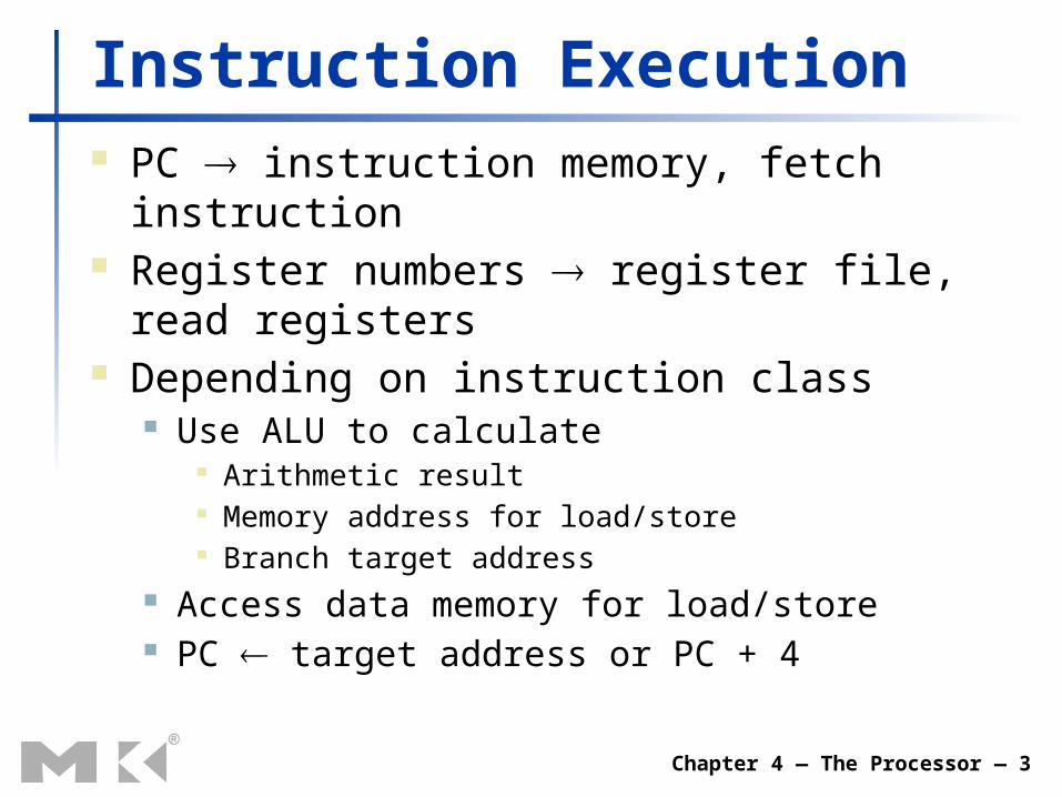
Clocking Methodology Combinational logic transforms data during
clock cycles Between clock edges Input from state elements, output to state
element Longest delay determines clock period

Chapter 4 — The Processor — 12
Building a Datapath Datapath
Elements that process data and addressesin the CPU
Registers, ALUs, mux’s, memories, …
We will build a MIPS datapath incrementally Refining the overview design
§4.3 Building a D
atapath
Chapter 4 — The Processor — 13
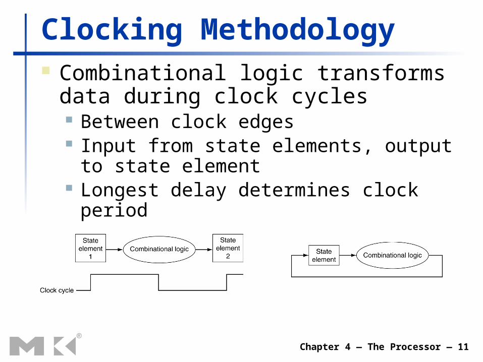
Instruction Fetch
32-bit register
Increment by 4 for next instruction
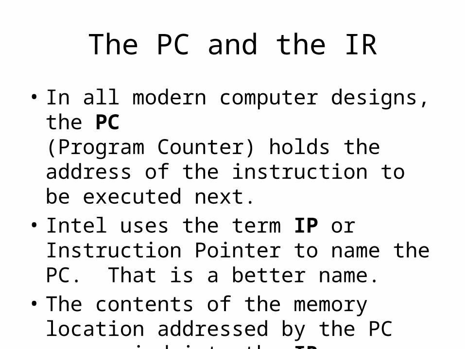
The PC and the IR
• In all modern computer designs, the PC (Program Counter) holds the address of the instruction to be executed next.
• Intel uses the term IP or Instruction Pointer to name the PC. That is a better name.
• The contents of the memory location addressed by the PC are copied into the IR (Instruction Register).
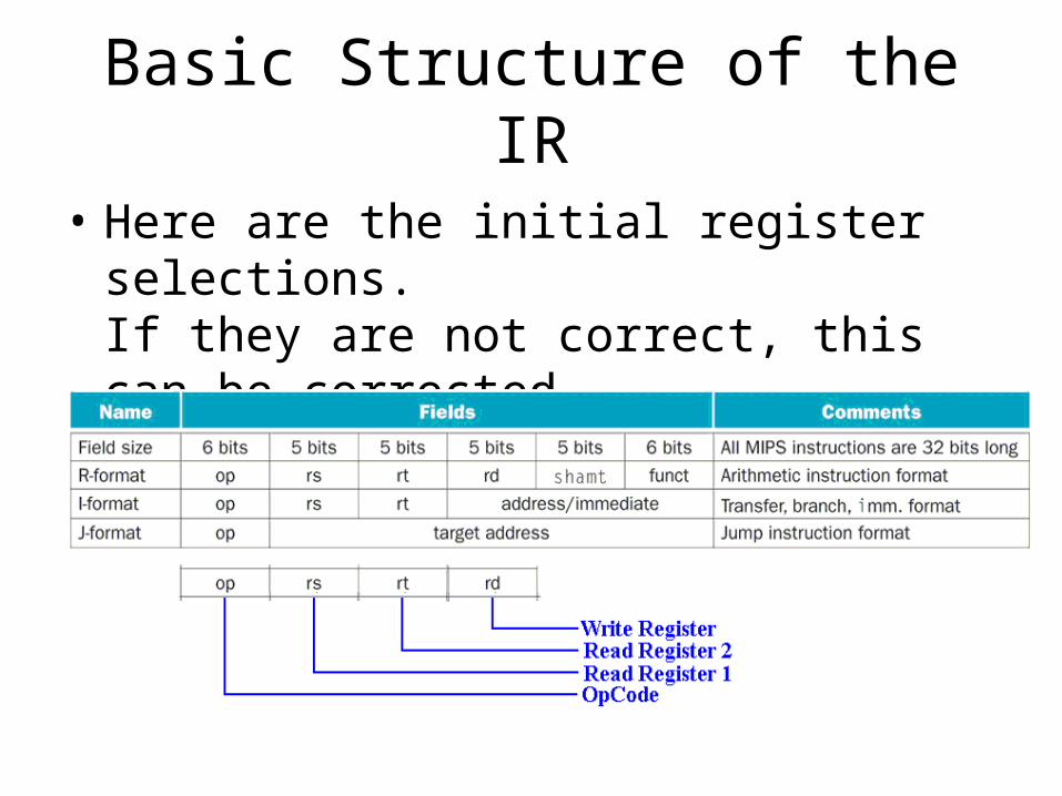
Basic Structure of the IR
• Here are the initial register selections. If they are not correct, this can be corrected later. This does not work for load register.
Chapter 4 — The Processor — 16
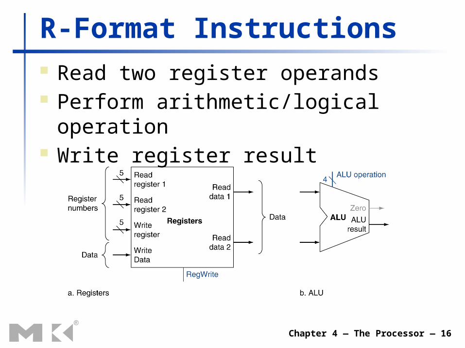
R-Format Instructions Read two register operands Perform arithmetic/logical operation Write register result
Chapter 4 — The Processor — 17
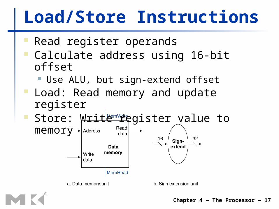
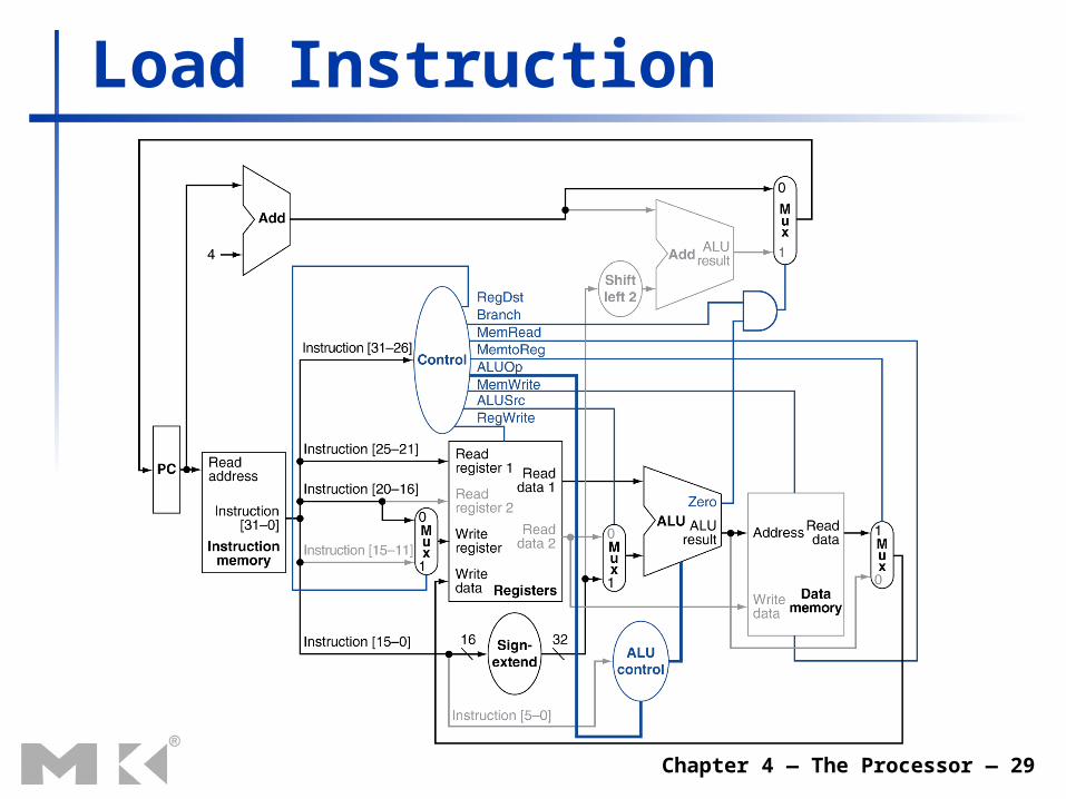
Load/Store Instructions Read register operands Calculate address using 16-bit offset
Use ALU, but sign-extend offset Load: Read memory and update register Store: Write register value to memory
Chapter 4 — The Processor — 18
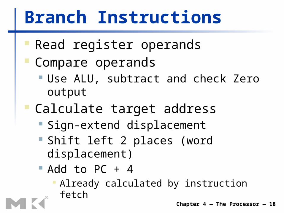
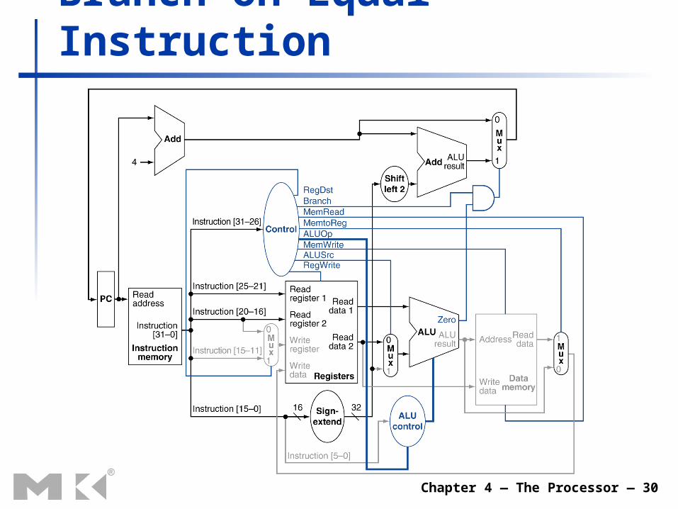
Branch Instructions Read register operands Compare operands
Use ALU, subtract and check Zero output Calculate target address
Sign-extend displacement Shift left 2 places (word displacement) Add to PC + 4
Already calculated by instruction fetch

Chapter 4 — The Processor — 19
Branch Instructions
Justre-routes
wires
Sign-bit wire replicated

Chapter 4 — The Processor — 20
Composing the Elements First-cut data path does an instruction in
one clock cycle Each datapath element can only do one
function at a time Hence, we need separate instruction and data
memories Use multiplexers where alternate data
sources are used for different instructions

Chapter 4 — The Processor — 21
R-Type/Load/Store Datapath
Chapter 4 — The Processor — 22
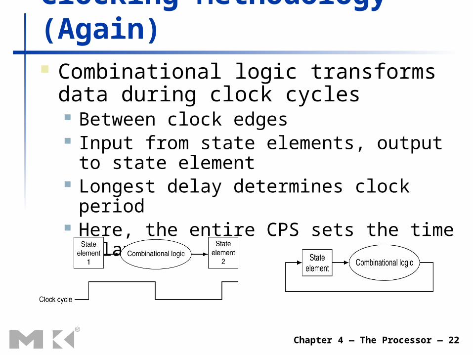
Clocking Methodology (Again) Combinational logic transforms data during
clock cycles Between clock edges Input from state elements, output to state
element Longest delay determines clock period Here, the entire CPS sets the time delay.
Chapter 4 — The Processor — 23
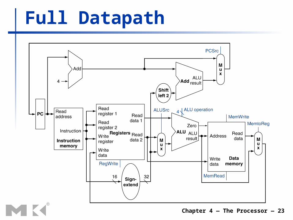
Full Datapath

Chapter 4 — The Processor — 24
ALU Control ALU used for
Load/Store: F = add Branch: F = subtract R-type: F depends on funct field
§4.4 A S
imple Im
plementation S
cheme
ALU control Function
0000 AND
0001 OR
0010 add
0110 subtract
0111 set-on-less-than
1100 NOR
Chapter 4 — The Processor — 25
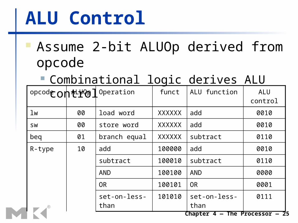
ALU Control Assume 2-bit ALUOp derived from opcode
Combinational logic derives ALU control
opcode ALUOp Operation funct ALU function ALU control
lw 00 load word XXXXXX add 0010
sw 00 store word XXXXXX add 0010
beq 01 branch equal XXXXXX subtract 0110
R-type 10 add 100000 add 0010
subtract 100010 subtract 0110
AND 100100 AND 0000
OR 100101 OR 0001
set-on-less-than 101010 set-on-less-than 0111
Chapter 4 — The Processor — 26
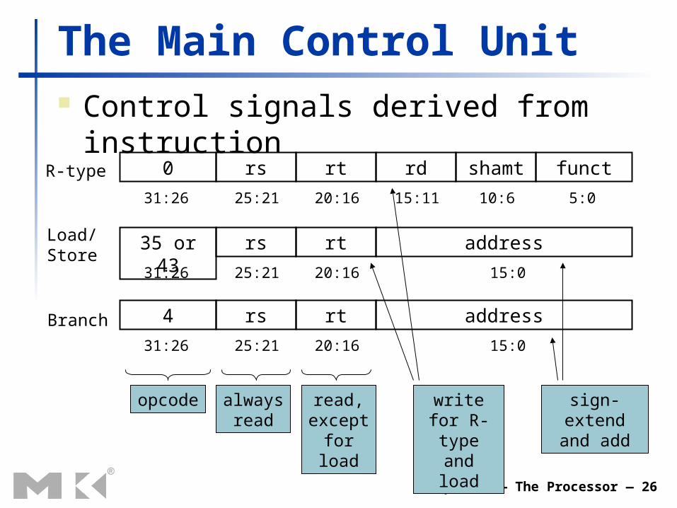
The Main Control Unit Control signals derived from instruction
0 rs rt rd shamt funct
31:26 5:025:21 20:16 15:11 10:6
35 or 43 rs rt address
31:26 25:21 20:16 15:0
4 rs rt address
31:26 25:21 20:16 15:0
R-type
Load/Store
Branch
opcode always read
read, except for load
write for R-type
and load
sign-extend and add

Chapter 4 — The Processor — 27
Datapath With Control

Chapter 4 — The Processor — 28
R-Type Instruction
Chapter 4 — The Processor — 29
Load Instruction
Chapter 4 — The Processor — 30
Branch-on-Equal Instruction
Chapter 4 — The Processor — 31
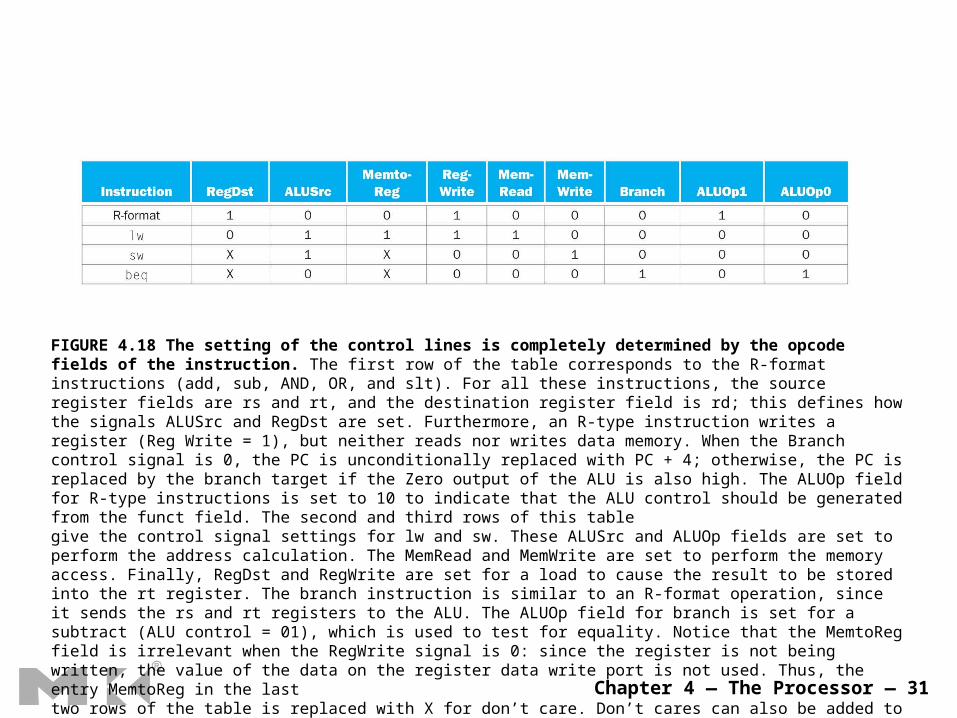
FIGURE 4.18 The setting of the control lines is completely determined by the opcode fields of the instruction. The first row of the table corresponds to the R-format instructions (add, sub, AND, OR, and slt). For all these instructions, the source register fields are rs and rt, and the destination register field is rd; this defines how the signals ALUSrc and RegDst are set. Furthermore, an R-type instruction writes a register (Reg Write = 1), but neither reads nor writes data memory. When the Branch control signal is 0, the PC is unconditionally replaced with PC + 4; otherwise, the PC is replaced by the branch target if the Zero output of the ALU is also high. The ALUOp field for R-type instructions is set to 10 to indicate that the ALU control should be generated from the funct field. The second and third rows of this tablegive the control signal settings for lw and sw. These ALUSrc and ALUOp fields are set to perform the address calculation. The MemRead and MemWrite are set to perform the memory access. Finally, RegDst and RegWrite are set for a load to cause the result to be stored into the rt register. The branch instruction is similar to an R-format operation, since it sends the rs and rt registers to the ALU. The ALUOp field for branch is set for a subtract (ALU control = 01), which is used to test for equality. Notice that the MemtoReg field is irrelevant when the RegWrite signal is 0: since the register is not being written, the value of the data on the register data write port is not used. Thus, the entry MemtoReg in the lasttwo rows of the table is replaced with X for don’t care. Don’t cares can also be added to RegDst when RegWrite is 0. This type of don’t care must be added by the designer, since it depends on knowledge of how the datapath works. Copyright © 2009 Elsevier, Inc. All rights reserved.
Chapter 4 — The Processor — 32
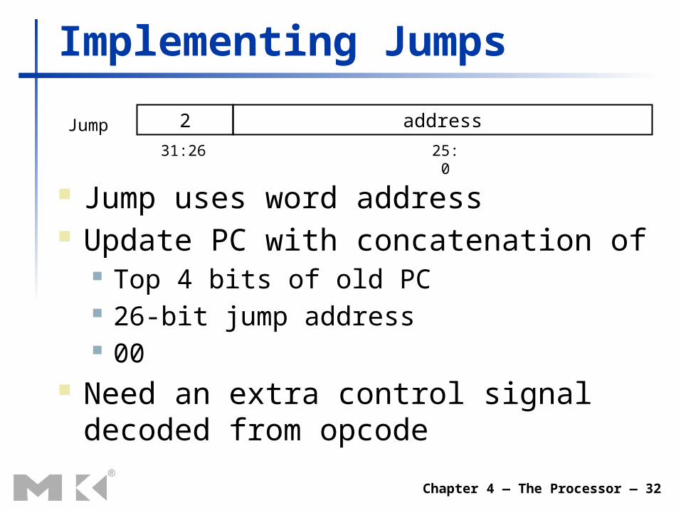
Implementing Jumps
Jump uses word address Update PC with concatenation of
Top 4 bits of old PC 26-bit jump address 00
Need an extra control signal decoded from opcode
2 address
31:26 25:0
Jump

Chapter 4 — The Processor — 33
Datapath With Jumps Added

Chapter 4 — The Processor — 34
Performance Issues Longest delay determines clock period
Critical path: load instruction Instruction memory register file ALU data
memory register file Not feasible to vary period for different
instructions Violates design principle
Making the common case fast We will improve performance by pipelining

The Multi-Cycle CPU
• We now discuss a design that has been omitted from the recent editions of the text.
• This is a “multi-cycle” design in which the execution of each instruction is divided into phases; each phase taking one clock pulse.
• Our overview of this design will lead into our discussion of pipelining.

The Multi-Cycle CPU
• We have just seen that a CPU designed to complete the execution of each instruction in a single clock cycle has two properties:
• 1. It is easy to design and easy to understand, and• 2. It is unacceptably slow.• We say that the single–cycle CPU has CPI = 1; one clock
cycle per instruction.• We now show a design in which CPI >1, in fact CPI 4. • The measure to minimize is the product
CPI (Clock cycle time).

The Multi-Cycle Datapath
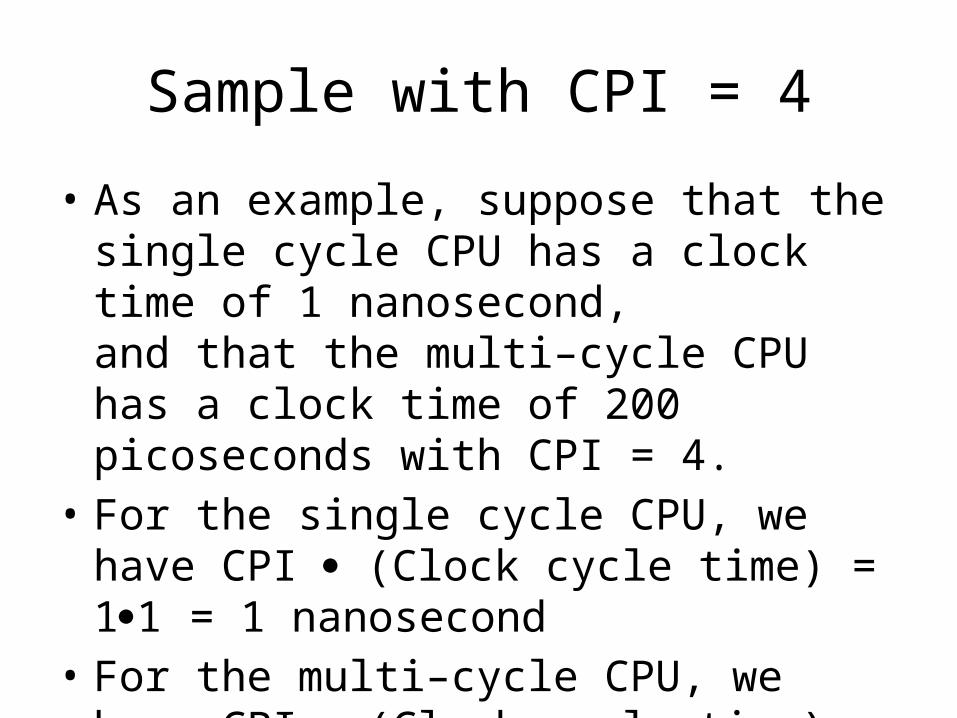
Sample with CPI = 4
• As an example, suppose that the single cycle CPU has a clock time of 1 nanosecond,and that the multi–cycle CPU has a clock time of 200 picoseconds with CPI = 4.
• For the single cycle CPU, we have CPI (Clock cycle time) = 11= 1 nanosecond
• For the multi–cycle CPU, we have CPI (Clock cycle time) = 40.2 = 0.8 nanosecond
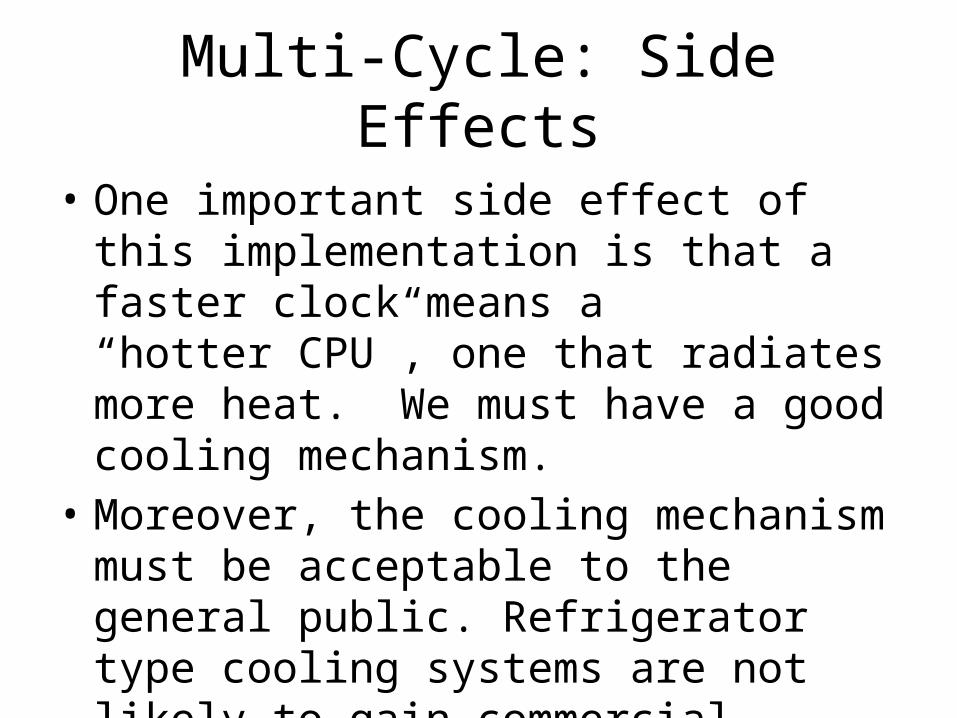
Multi-Cycle: Side Effects
• One important side effect of this implementation is that a faster clock means a“hotter CPU”, one that radiates more heat. We must have a good cooling mechanism.
• Moreover, the cooling mechanism must be acceptable to the general public. Refrigerator type cooling systems are not likely to gain commercial acceptance for a home computer.
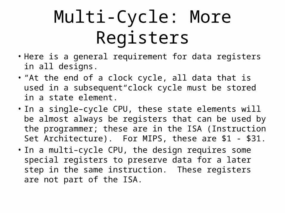
Multi-Cycle: More Registers
• Here is a general requirement for data registers in all designs.
• “At the end of a clock cycle, all data that is used in a subsequent clock cycle must be stored in a state element.”
• In a single–cycle CPU, these state elements will be almost always be registers that can be used by the programmer; these are in the ISA (Instruction Set Architecture). For MIPS, these are $1 - $31.
• In a multi–cycle CPU, the design requires some special registers to preserve data for a later step in the same instruction. These registers are not part of the ISA.
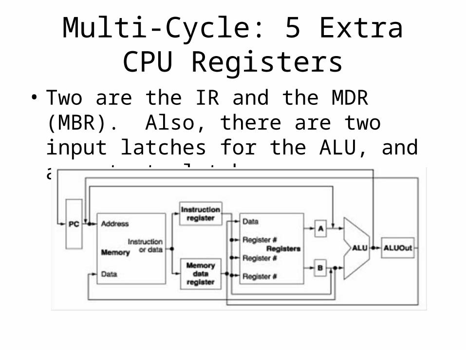
Multi-Cycle: 5 Extra CPU Registers
• Two are the IR and the MDR (MBR). Also, there are two input latches for the ALU, and an output latch.
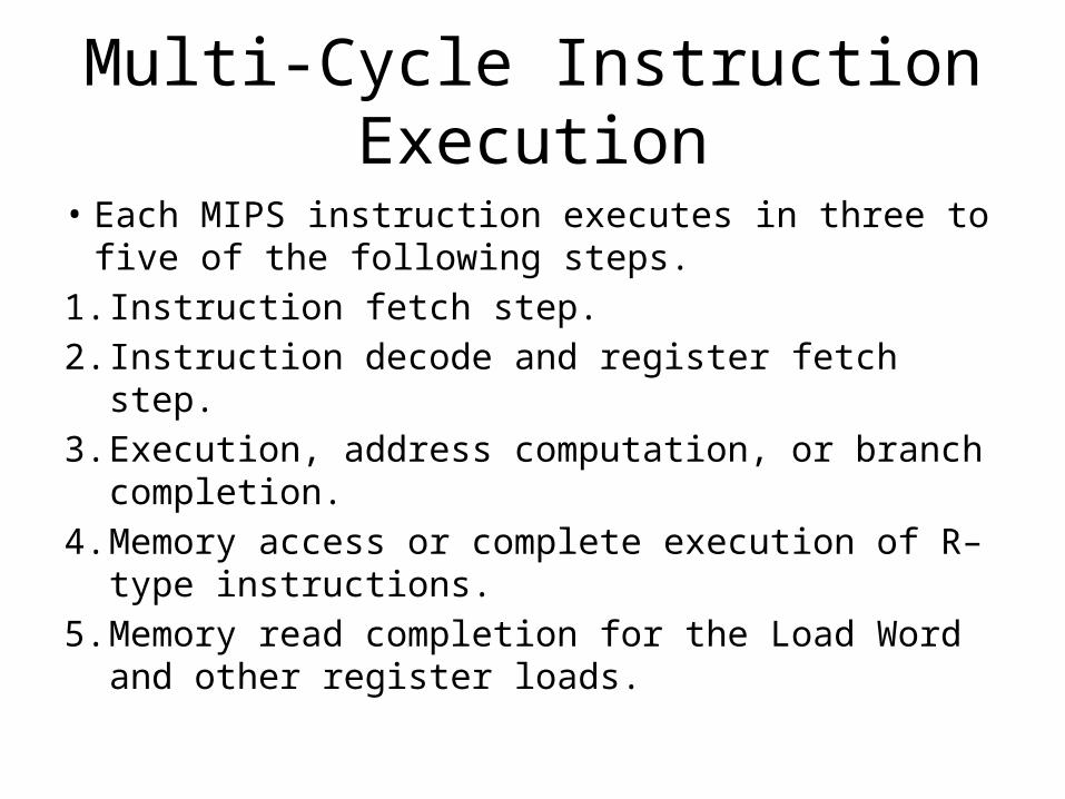
Multi-Cycle Instruction Execution
• Each MIPS instruction executes in three to five of the following steps.
1. Instruction fetch step.2. Instruction decode and register fetch step.3. Execution, address computation, or branch
completion.4. Memory access or complete execution of R–type
instructions.5. Memory read completion for the Load Word and
other register loads.

Multi-Cycle Implementation (Step 1)
• 1. Instruction fetch step• IR <= Memory[PC]• PC <= PC + 4• The instruction is read into the IR and the PC is
incremented by 4 to point to the next instruction.
• A branch or jump instruction will update the PC on a later clock cycle.

Multi-Cycle Implementation (Step 2)
• 2. Instruction decode, register fetch and compute target address
• IR[31:26] copied to the Control Unit and decoded• A <= Register[IR[25:21]]• B <= Register[IR[20:16]]• ALUOut <= PC + ( sign_extend(IR[15:0] << 2)• At the end of this step, the instruction will have been
identified by the control unit.• At this point, the CPU performs a number of operations
that are likely to be useful, since they can be proven not to be harmful.

Multi-Cycle Implementation (Step 3)
• 3. Execute R–type instructions, compute address, or complete the branch.
• At this point the control unit has decoded the instruction, so that the datapath operations are now determined by the type of instruction. We have 4 possible operations types.
• BranchIf Zero Then PC <= ALUOut, Else no action.The ALU takes in the contents of the A and B latches, and subtracts. It asserts the discrete signal Zero if (A – B) is zero. If (A == B) the PC is updated to point to the branch target, otherwise the PC is not updated. This instruction ends and the next instruction is fetched.
Multi-Cycle Implementation (Step 3)
• Jump• PC <= PC[31:28] ¢ IR[25:0] ¢ 00• This is an unconditional jump; the value of the
Program Counter is replaced by the jump address, this instruction ends, and the next instruction is fetched.

Multi-Cycle Implementation (Step 3)
• Execute R–type instruction• ALUOut <= A op B• The contents of the A and B registers are
passed to the ALU and the indicated operation is performed. The result is written to the ALUOut register, overwriting the result from step 2 (which produced a jump target).
• Execution continues in step 4.

Multi-Cycle Implementation (Step 3)
• Memory Address Computation• ALUOut <= A + sign_extend(IR[15:0])• The contents of the A register and the sign extended
value of the address offset, found in IR[15:0] are input to the ALU.The ALU performs an addition and outputs the result in the ALUOut register.
• The value in the ALUOut register will be used as a memory address for either a register load or register store. Execution continues in step 4.
Multi-Cycle Implementation (Step 4)
• Here the CPU has three options, two of which are related to memory reference.
• Complete R–type instruction• Register[IR[15:11]] <= ALUOut• Here the contents of the ALUOut register,
containing the value computed in step 3, are written to the destination register. The instruction ends and the next instruction fetched.

Multi-Cycle Implementation (Step 4)
• Memory Reference: Store Word• Memory[ALUOut] <= B• Here the contents of the ALUOut register are used
as a memory address. The contents of the B register are copied directly to the memory input Write Data, and the discrete control signal MemWrite asserted to initiate update of the addressed memory word.The instruction ends and the next instruction is fetched.
Multi-Cycle Implementation (Step 4)
• Memory Reference: Load Word• MDR <= Memory[ALUOut]• Here the contents of the ALUOut register are
used as a memory address, the address of the word to be copied into the MDR. The discrete signal MemRead is asserted, causing the memory to be read and the MDR to be updated automatically.
Multi-Cycle Implementation (Step 5)
• Only the register load instructions require this step.• 5. Load register from memory• Register[IR[20:16]] <= MDR• The multiplexer feeding the Write Data input to the
register file is set to copy the contents of the Memory Data Register into the target general–purpose register. The discrete control signal RegDst is not asserted, so the target register is selected by IR[20:16].
• The instruction ends and the next instruction is fetched.