
Design Workbook - NXP
46
1 Introduction This document describes the design information on the MVP reference platform. MVP, short for M ultiprocessing V erification P latform, is a dual-processor MPC7450-based platform which allows evaluation of the 60X or MPX bus interfaces. It provides all necessary computing platform devices needed to boot Linux, QNX, VxWorks, or other OSes. This version of the design document describes the “X2” version, which has slight architectural changes over the first X1 version. Design Workbook MVPX2DW/D Rev. 0.3, 11/2001 MVP X2 Multiprocessor Evaluation System Design Workbook Gary Milliorn CPD Applications
Transcript of Design Workbook - NXP
Design Workbook
MVPX2DW/DRev. 0.3, 11/2001
MVP X2 Multiprocessor Evaluation SystemDesign Workbook
Gary MilliornCPD Applications
1 IntroductionThis document describes the design information on the MVP reference platform. MVP, shortfor Multiprocessing Verification Platform, is a dual-processor MPC7450-based platformwhich allows evaluation of the 60X or MPX bus interfaces. It provides all necessarycomputing platform devices needed to boot Linux, QNX, VxWorks, or other OSes.
This version of the design document describes the “X2” version, which has slight architecturalchanges over the first X1 version.
Features
1.1 FeaturesThe MVP includes the following features:
• Two MPC745X Processors (MPC7450 or MPC7451 “V’ger” or compatible)
– 2MB pipelined-burst (PB) L3 Cache
• GD64260 System Controller (“Discovery”)
– Dual Processor (60X bus mode) or Single-processor (MPX bus mode) interface
– SDRAM controller
– Dual PCI Interfaces
– Dual 10/100base-T Ethernet interfaces
– Dual serial ports
• SDRAM Modules
– 2 PC133 SDRAM DIMM sockets
– 2GB maximum memory (256MB standard)
• PCI Interface #1
– Two slots, 32 or 64 bit, 66 MHz, 3V
• PCI Interface #2
– Two slots, 32 bit, 33 MHz, 5V
• Super IO
– Dual USB 1.0/UHCI v1.1 interface
– Dual UltraDMA 33 IDE Disk interface
– PS/2 keyboard and mouse interfaces
• Flash/ROM Interface
– 32-bit Boot ROM (1-16 MB, 8 MB standard)
– 32-bit OS/User ROM (1-16 MB, 8 MB standard)
• Ethernet
– Dual 10/100baseT Ethernet
• Dual UART
– Standard 9-pin serial port, baud rates up to ~500kpbs
• Power Supplies
– Individual 18A 1.3 to 2.5V switching power supplies for each MPC7450
– Adjustable 10A 1.8V and 2.5V switching power supplies for L3 cache, Discovery, etc.
• ATX Motherboard Form-factor
2 MVP X2 Multiprocessor Evaluation System Design Workbook MOTOROLA
Overview
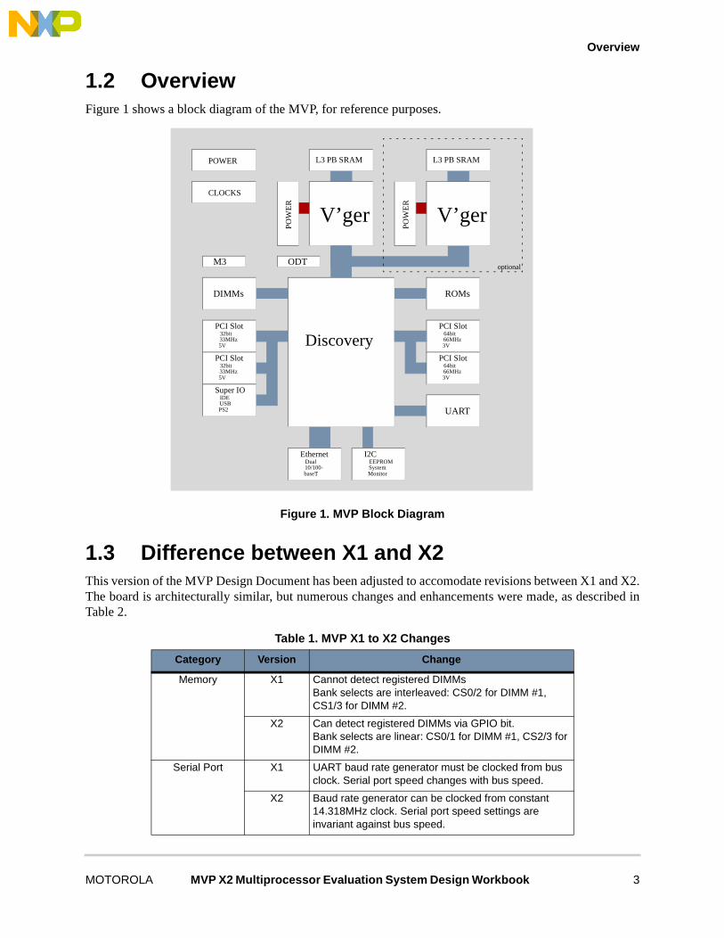
1.2 OverviewFigure 1 shows a block diagram of the MVP, for reference purposes.
Figure 1. MVP Block Diagram
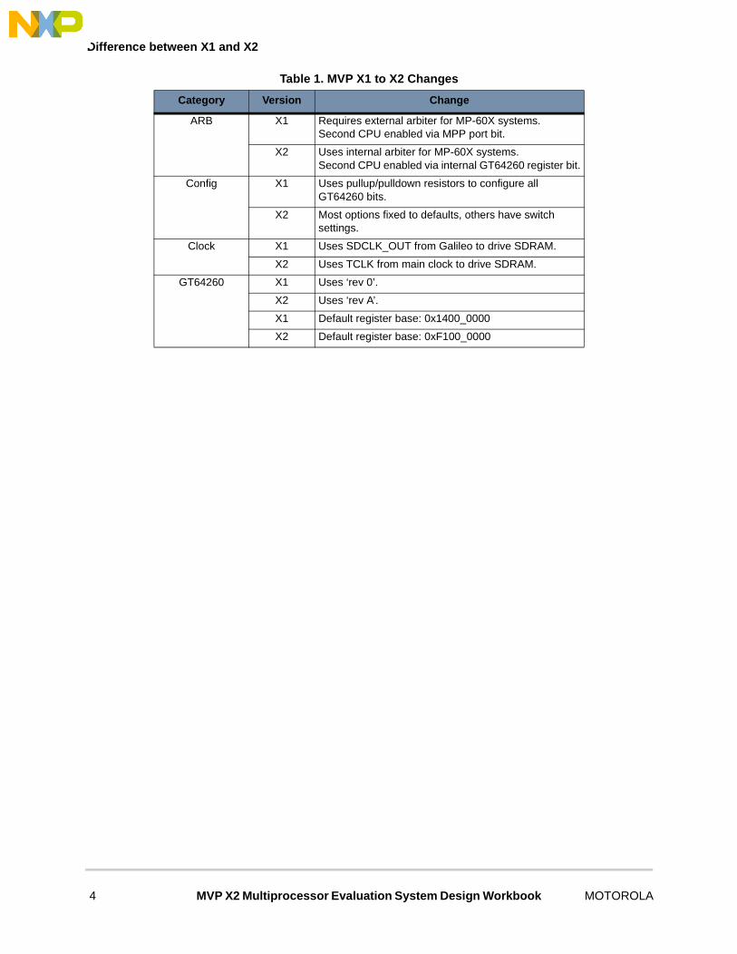
1.3 Difference between X1 and X2This version of the MVP Design Document has been adjusted to accomodate revisions between X1 and X2.The board is architecturally similar, but numerous changes and enhancements were made, as described inTable 2.
Table 1. MVP X1 to X2 Changes
Category Version Change
Memory X1 Cannot detect registered DIMMsBank selects are interleaved: CS0/2 for DIMM #1, CS1/3 for DIMM #2.
X2 Can detect registered DIMMs via GPIO bit.Bank selects are linear: CS0/1 for DIMM #1, CS2/3 for DIMM #2.
Serial Port X1 UART baud rate generator must be clocked from bus clock. Serial port speed changes with bus speed.
X2 Baud rate generator can be clocked from constant 14.318MHz clock. Serial port speed settings are invariant against bus speed.
V’ger
L3 PB SRAM
POW
ER
Discovery
ROMs
optional
V’ger
L3 PB SRAM
POW
ER
DIMMs
PCI Slot64bit66MHz3V
PCI Slot64bit66MHz3V
PCI Slot32bit33MHz5V
PCI Slot32bit33MHz5V
Super IOIDEUSBPS2
EthernetDual10/100-baseT
POWER
CLOCKS
I2CEEPROMSystemMonitor
UART
ODTM3
MOTOROLA MVP X2 Multiprocessor Evaluation System Design Workbook 3
Difference between X1 and X2
ARB X1 Requires external arbiter for MP-60X systems.Second CPU enabled via MPP port bit.
X2 Uses internal arbiter for MP-60X systems.Second CPU enabled via internal GT64260 register bit.
Config X1 Uses pullup/pulldown resistors to configure all GT64260 bits.
X2 Most options fixed to defaults, others have switch settings.
Clock X1 Uses SDCLK_OUT from Galileo to drive SDRAM.
X2 Uses TCLK from main clock to drive SDRAM.
GT64260 X1 Uses ‘rev 0’.
X2 Uses ‘rev A’.
X1 Default register base: 0x1400_0000
X2 Default register base: 0xF100_0000
Table 1. MVP X1 to X2 Changes
Category Version Change
4 MVP X2 Multiprocessor Evaluation System Design Workbook MOTOROLA
Processors
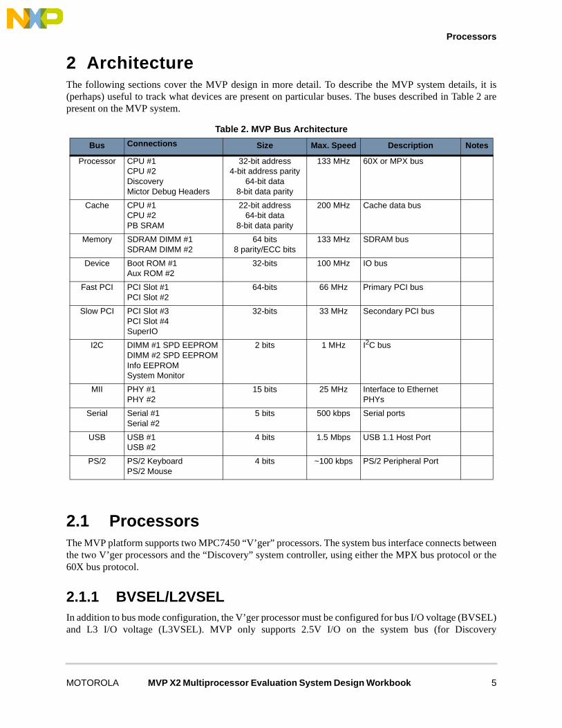
2 ArchitectureThe following sections cover the MVP design in more detail. To describe the MVP system details, it is(perhaps) useful to track what devices are present on particular buses. The buses described in Table 2 arepresent on the MVP system.
2.1 ProcessorsThe MVP platform supports two MPC7450 “V’ger” processors. The system bus interface connects betweenthe two V’ger processors and the “Discovery” system controller, using either the MPX bus protocol or the60X bus protocol.
2.1.1 BVSEL/L2VSELIn addition to bus mode configuration, the V’ger processor must be configured for bus I/O voltage (BVSEL)and L3 I/O voltage (L3VSEL). MVP only supports 2.5V I/O on the system bus (for Discovery
Table 2. MVP Bus Architecture
Bus Connections Size Max. Speed Description Notes
Processor CPU #1CPU #2DiscoveryMictor Debug Headers
32-bit address4-bit address parity
64-bit data8-bit data parity
133 MHz 60X or MPX bus
Cache CPU #1CPU #2PB SRAM
22-bit address64-bit data
8-bit data parity
200 MHz Cache data bus
Memory SDRAM DIMM #1SDRAM DIMM #2
64 bits8 parity/ECC bits
133 MHz SDRAM bus
Device Boot ROM #1Aux ROM #2
32-bits 100 MHz IO bus
Fast PCI PCI Slot #1PCI Slot #2
64-bits 66 MHz Primary PCI bus
Slow PCI PCI Slot #3PCI Slot #4SuperIO
32-bits 33 MHz Secondary PCI bus
I2C DIMM #1 SPD EEPROMDIMM #2 SPD EEPROMInfo EEPROMSystem Monitor
2 bits 1 MHz I2C bus
MII PHY #1PHY #2
15 bits 25 MHz Interface to Ethernet PHYs
Serial Serial #1Serial #2
5 bits 500 kbps Serial ports
USB USB #1USB #2
4 bits 1.5 Mbps USB 1.1 Host Port
PS/2 PS/2 KeyboardPS/2 Mouse
4 bits ~100 kbps PS/2 Peripheral Port
MOTOROLA MVP X2 Multiprocessor Evaluation System Design Workbook 5
System Controller
compatibility) and 2.5V I/O on the L3 bus (for PB2 compatibility), so these options are not switch/resistorsselectable on MVP.
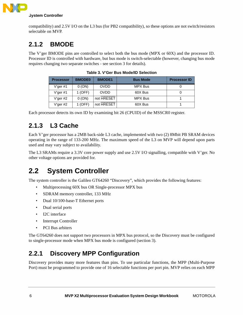
2.1.2 BMODEThe V’ger BMODE pins are controlled to select both the bus mode (MPX or 60X) and the processor ID.Processor ID is controlled with hardware, but bus mode is switch-selectable (however, changing bus moderequires changing two separate switches - see section 3 for details).
Each processor detects its own ID by examining bit 26 (CPUID) of the MSSCR0 register.
2.1.3 L3 CacheEach V’ger processor has a 2MB back-side L3 cache, implemented with two (2) 8Mbit PB SRAM devicesoperating in the range of 133-200 MHz. The maximum speed of the L3 on MVP will depend upon partsused and may vary subject to availability.
The L3 SRAMs require a 3.3V core power supply and use 2.5V I/O signalling, compatible with V’ger. Noother voltage options are provided for.
2.2 System ControllerThe system controller is the Galileo GT64260 “Discovery”, which provides the following features:
• Multiprocessing 60X bus OR Single-processor MPX bus
• SDRAM memory controller, 133 MHz
• Dual 10/100-base-T Ethernet ports
• Dual serial ports
• I2C interface
• Interrupt Controller
• PCI Bus arbiters
The GT64260 does not support two processors in MPX bus protocol, so the Discovery must be configuredto single-processor mode when MPX bus mode is configured (section 3).
2.2.1 Discovery MPP ConfigurationDiscovery provides many more features than pins. To use particular functions, the MPP (Multi-PurposePort) must be programmed to provide one of 16 selectable functions per port pin. MVP relies on each MPP
Table 3. V’Ger Bus Mode/ID Selection
Processor BMODE0 BMODE1 Bus Mode Processor ID
V’ger #1 0 (ON) OVDD MPX Bus 0
V’ger #1 1 (OFF) OVDD 60X Bus 0
V’ger #2 0 (ON) not HRESET MPX Bus 1
V’ger #2 1 (OFF) not HRESET 60X Bus 1
6 MVP X2 Multiprocessor Evaluation System Design Workbook MOTOROLA

System Controller
port being set to the proper configuration option as described in Table 4; otherwise, the system may notoperate properly.
Table 4. MVP MPP Usage
MPP Bit MPP DefinitionMPP
ProgrammingUsage Notes
0 GNT0[0]* MPPCTL0[3:0] pPCI slot 1 GNT#
1 REQ0[0]* MPPCTL0[7:4] pPCI slot 1 REQ#
2 GNT0[1]* MPPCTL0[11:8] pPCI slot 2 GNT#
3 REQ0[1]* MPPCTL0[15:12] pPCI slot 2 REQ#
4 GPP[4] MPPCTL0[19:16] Cross-processor 1->0 interrupt
5 GPP[5] MPPCTL0[23:20] Cross-processor 0->1 output drive
6 GPP[6] MPPCTL0[27:24] pPCI INT 0 (Slot 1 INTA#, Slot 2 INTD#)
7 GPP[7] MPPCTL0[31:28] pPCI INT 1 (Slot 1 INTB#, Slot 2 INTA#)
8 GPP[8] MPPCTL1[3:0] pPCI INT 2 (Slot 1 INTC#, Slot 2 INTB#)
9 GPP[9] MPPCTL1[7:4] pPCI INT 3 (Slot 1 INTD#, Slot 2 INTC#)
10 GPP[10] MPPCTL1[11:8] sPCI INT 0 (Slot 3 INTA#, Slot 4 INTD#)
11 GPP[11] MPPCTL1[15:12] sPCI INT 1 (Slot 3 INTB#, Slot 4 INTA#)
12 GPP[12] MPPCTL1[19:16] sPCI INT 2 (Slot 3 INTC#, Slot 4 INTB#)
13 GPP[13] MPPCTL1[23:20] sPCI INT 3 (Slot 3 INTD#, Slot 4 INTC#)
14 GPP[14] MPPCTL1[27:24] PHY1 INT*
15 GPP[15] MPPCTL1[31:28] PHY2 INT*
16 GNT1[0]* MPPCTL2[3:0] sPCI slot 3 GNT#
17 REQ1[0]* MPPCTL2[7:4] sPCI slot 3 REQ#
18 GNT1[1]* MPPCTL2[11:8] sPCI slot 4 GNT#
19 REQ1[1]* MPPCTL2[15:12] sPCI slot 4 REQ#
20 GNT2[1]* MPPCTL2[19:16] sPCI SIO GNT#
21 REQ2[1]* MPPCTL2[23:20] sPCI SIO REQ#
22 GPP[22] MPPCTL2[27:24] SIOINT 1
23 GPP[23] MPPCTL2[31:28] BG1_EN 2
24 GPP[24] MPPCTL3[3:0] SYSSTAT 3
25 GPP[25] MPPCTL3[7:4] REGE 5
26 GPP[26] MPPCTL3[11:8] reserved 4
27 GPP[27] MPPCTL3[15:12] reserved 4
28 GPP[28] MPPCTL3[19:16] reserved 4
29 GPP[29] MPPCTL3[23:20] reserved
30 GPP[30] MPPCTL3[27:24] Cross-processor 0->1 interrupt
31 GPP[31] MPPCTL3[31:28] Cross-processor 1->0 output drive
MOTOROLA MVP X2 Multiprocessor Evaluation System Design Workbook 7
MVP FPGAs
NOTES:1 Active high interrupt.2 GPIO signal set to output; active high enables secondary processor if external arbiter option is used.3 LED drive output; set to active low output.4 Reserved pin; set to input.5 Registered mode DIMM detect (common to both slots). 1 = registered; 0 = normal.
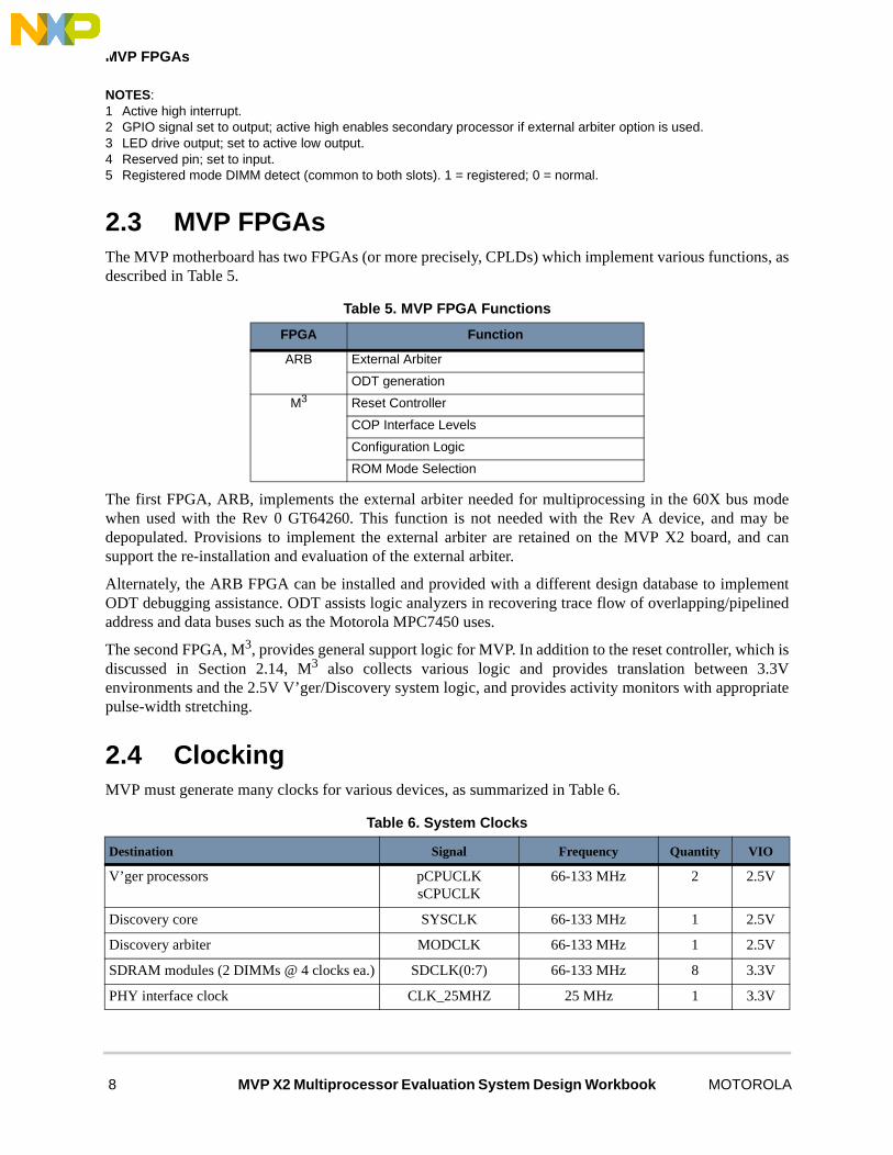
2.3 MVP FPGAsThe MVP motherboard has two FPGAs (or more precisely, CPLDs) which implement various functions, asdescribed in Table 5.
The first FPGA, ARB, implements the external arbiter needed for multiprocessing in the 60X bus modewhen used with the Rev 0 GT64260. This function is not needed with the Rev A device, and may bedepopulated. Provisions to implement the external arbiter are retained on the MVP X2 board, and cansupport the re-installation and evaluation of the external arbiter.
Alternately, the ARB FPGA can be installed and provided with a different design database to implementODT debugging assistance. ODT assists logic analyzers in recovering trace flow of overlapping/pipelinedaddress and data buses such as the Motorola MPC7450 uses.
The second FPGA, M3, provides general support logic for MVP. In addition to the reset controller, which isdiscussed in Section 2.14, M3 also collects various logic and provides translation between 3.3Venvironments and the 2.5V V’ger/Discovery system logic, and provides activity monitors with appropriatepulse-width stretching.
2.4 ClockingMVP must generate many clocks for various devices, as summarized in Table 6.
Table 5. MVP FPGA Functions
FPGA Function
ARB External Arbiter
ODT generation
M3 Reset Controller
COP Interface Levels
Configuration Logic
ROM Mode Selection
Table 6. System Clocks
Destination Signal Frequency Quantity VIO
V’ger processors pCPUCLKsCPUCLK
66-133 MHz 2 2.5V
Discovery core SYSCLK 66-133 MHz 1 2.5V
Discovery arbiter MODCLK 66-133 MHz 1 2.5V
SDRAM modules (2 DIMMs @ 4 clocks ea.) SDCLK(0:7) 66-133 MHz 8 3.3V
PHY interface clock CLK_25MHZ 25 MHz 1 3.3V
8 MVP X2 Multiprocessor Evaluation System Design Workbook MOTOROLA

Clocking
Since several of these clocks are completely independent of other clocks, they are generated by simpleoscillator components where possible. This has the additional advantage of minimizing the amount of clocktraces running over the MVP board, but it is not necessarily the most cost-effective solution. Integratedclock synthesizers can also provide such clocks where board space or cost is at a premium.
The overall clock architecture is shown in Figure 2.
Figure 2. MVP Clock Architecture
The main clocks are generated by the Motorola MPC972, a PLL-based clock multiplier that meets allMotorola MPC7450X restrictions (in particular, low jitter and fast rise/fall time). MVP uses a MotorolaMPC961 clock regenerator to drive the SDRAM clocks (up to four per module), which provides the systemwith the ability to adjust the skew between the Discovery and the SDRAM with configurable path delays;this may be required to operate at high speeds with large memory arrays.
Fast PCI clocks pPCICLK(0:3)
pPCICLK0 = slot1pPCICLK1 = slot2pPCICLK2 = rsvpPCICLK3 = pPCI
33-100 MHz 4 3.3V
Slow PCI clocks sPCICLK(0:3)
sPCICLK0 = slot3sPCICLK1 = slot4sPCICLK2 = SIOsPCICLK3 = PCI
25-66 MHz 4 3.3V
USB Clock CLK_48MHZ 48 MHz 1 5V
SIO Clock CLK_14MHZ 14.318 MHz 1 5V
Table 6. System Clocks
Destination Signal Frequency Quantity VIO
UART
2.5V
OSC
OSC
OSC
GT64260
DIMM #1
DIMM #2
MP
C96
1CtuningsCPU
pCPU
sPCI
pPCI
SIO
MPC972
SSCGOSC
2.5V
3.3V
3.3VPHY
USB
SIO
MOTOROLA MVP X2 Multiprocessor Evaluation System Design Workbook 9

Clocking
A complication of using the MPC972 or many common clock synthesizers is that the V’ger and Discoveryrequire 2.5V clocks. Instead of buffering the clocks, which would cause unacceptable phase delay, MVPuses resistor dividers which reduce the voltage at the destination to 2.5V in a manner compatible with a 55ohm impedance board. The divider network is shown in Figure 3.
Figure 3. MVP Clock Resistor Dividers
The MPC972 uses programmable divider options to synthesize clocks using divisions of a high-frequencyinternal VCO. Consequently, there are literally hundreds of combinations, though many are not usable. Thetable shown in Table 7 lists some of the more useful combinations; other combinations can be derived fromthe MPC972 hardware specification if custom frequencies are needed.
NOTES:0 = ON = UP (viewed with I/O connectors at top of board)1 = OFF = DOWN
2.4.1 Spread-Spectrum ClockMVP includes a spread-spectrum modulated clock which dynamically alters the base frequency of the CPU,system memory and PCI bus clocks (other clocks are unaffected). This option is useful for attainingFCC/VDE compliance with radiated emissions. Only the minimum spread range, +/- 0.625%, is guaranteedto meet the MPC745X clock input jitter requirements, though higher spreads are possible if the maximumsystem frequency is not selected.
Table 7. System Clock Selection
CPU &Memory Bus
Speed
Fast/3V PCI Bus Speed
Slow/5V PCI Bus Speed
SW7 Settings
133 MHz 66 MHz 33 MHz 0100 0010
100 MHz 66 MHz 33 MHz 1111 1010
100 MHz 33 MHz 33 MHz 1010 1000
83 MHz 55 MHz 41 MHz 0111 1101
66 MHz 66 MHz 33 MHz 0101 0101
66 MHz 33 MHz 33 MHz 0000 0001
Rx=51ΩCLOCK
Ry=175Ω
CLKIN
10 MVP X2 Multiprocessor Evaluation System Design Workbook MOTOROLA

Memory
2.5 MemoryThe MVP system provides memory resources described in Table 8.
NOTES:1 The maximum speed of SDRAM may be dependant on availablility of particular revisions of silicon; refer to the
system configuration sheet for details).2 There are two separate 16MB flash devices at the addresses shown; the total size is 32MB.3 Access to NVRAM is via an address/data register in the real-time-clock component of the VIA SuperIO.
2.5.1 SDRAMMVP supports one or two standard PC-100/PC-133, 3.3 Volt, single-data-rate SDRAM DIMM sockets.Each socket connects to two separate bank enables on the Discovery system controller, and each bank maybe up to 1GB in size, so a total of up to 4GB may be supported. Figure 4 shows a block diagram of theSDRAM memory architecture.
Figure 4. SDRAM Architecture
The connections between Discovery and the SDRAM sockets are fairly straightforward. Except for thedatabus, most SDRAM signals are output only and may be routed in a daisy-chain from Discovery to eachDIMM socket, keeping overall trace lengths short, paired and separated by at least 6-12 mils. Signals aresource-series-terminated with impedance matching resistors; no other termination is used.
The DIMM clocks are generated by an MPC961, which generates in-phase copies of the SDCLK (SDRAMclock) that is matched to the Discovery system clock (SYSCLK).
Table 8. .MVP Memory Resources
Type Size SpeedAddress Range
Memory Range Notes
SDRAM 0 .. 2GB 33 ... 133 MHz Direct 0000_0000 ... 3FFF_FFFF 1
Flash 32 MB 33 ... 133 MHz Direct FF00_0000 ... FF7F_FFFFFF80_0000 ... FFFF_FFFF
2
NVRAM 256 B 33 MHz Indirect XX00_0072 ... XX00_0073 3
EEPROM
256 B 1 MHz Serial 00 ... FF
MPC961C
to D
isco
very
MA[12:0]BA[1:0SDRASSDCASSDWE
DQM[7:0]MD[63:0]
SCS0, SCS2
SDCLK
SCS1, SCS3
DIM
M
MOTOROLA MVP X2 Multiprocessor Evaluation System Design Workbook 11
Flash Memory
Registered mode SDRAM DIMMs are supported and can be enabled with an external configuration switch.Since Discovery does not support low-power modes, CKE is not supported and is simply tied high for eachmodule.
Since DIMMs are available in one- or two-physical bank configurations, MVP interleaves the chip selectsprovided to the sockets so that either type may be supported. No matter how the multiple DIMM chip selectsare connected, software must be aware to the possibility of mixed single- and dual-bank DIMMs andmanage chip selects accordingly, as shown in Table 9.
NOTES:1 Single-bank DIMMs are generally preferred for higher-speed operation, especially at 133 MHz.
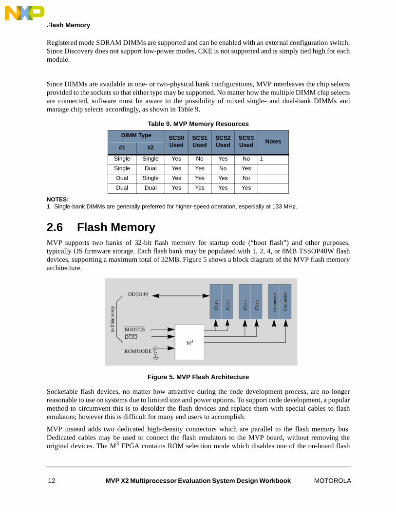
2.6 Flash MemoryMVP supports two banks of 32-bit flash memory for startup code (“boot flash”) and other purposes,typically OS firmware storage. Each flash bank may be populated with 1, 2, 4, or 8MB TSSOP48W flashdevices, supporting a maximum total of 32MB. Figure 5 shows a block diagram of the MVP flash memoryarchitecture.
Figure 5. MVP Flash Architecture
Socketable flash devices, no matter how attractive during the code development process, are no longerreasonable to use on systems due to limited size and power options. To support code development, a popularmethod to circumvent this is to desolder the flash devices and replace them with special cables to flashemulators; however this is difficult for many end users to accomplish.
MVP instead adds two dedicated high-density connectors which are parallel to the flash memory bus.Dedicated cables may be used to connect the flash emulators to the MVP board, without removing theoriginal devices. The M3 FPGA contains ROM selection mode which disables one of the on-board flash
Table 9. MVP Memory Resources
DIMM Type SCS0 Used
SCS1 Used
SCS2 Used
SCS3 Used
Notes#1 #2
Single Single Yes No Yes No 1
Single Dual Yes Yes No Yes
Dual Single Yes Yes Yes No
Dual Dual Yes Yes Yes Yes
Flas
h
BOOTCS
Flas
h
M3DCS3
DD[31:0]
ROMMODE
to D
isco
very Fl
ash
Flas
h
Con
nect
or
Con
nect
or
12 MVP X2 Multiprocessor Evaluation System Design Workbook MOTOROLA

PCI
banks and redirects accesses to the flash emulator, for transparent switching between on-board and off-boardflash.
To allow the emulator to intercept the standard flash controls, the M3 FPGA alters the definition of theBOOTCS and DCS3 chip selects from Discovery. Typically these signals are routed directly to thecomponent, but on MVP M3 alters them according to Table 10.
Using the ROMMODE option switches, startup code can be swapped among the flash memory banks, andeach bank can be redirected to the ROM emulator sockets for quick download. Note that both banks cannotbe emulated at the same time.
The flash may be sector-protected by applying +12V to the “SECPR” test pad and running appropriatesoftware. Neither DINK nor other software make any use of this facility at this time.
2.7 PCIThe Discovery supports two independant PCI buses, each configurable for 32 or 64-bit operation, and at 33or 66 MHz operation (among other frequencies). MVP separates the two buses into a high-speed3.3V/64-bit/66 MHz PCI bus and a slower 5V/32-bit/33 MHz bus, as shown in Figure 6. The latter busallows connection of the PCI-based VIA SuperIO, which only operates at 33 MHz.
Figure 6. MVP PCI Architecture
Table 10. Flash ROM Modes
ROMMODE(0:1) Mode Controls
00 Standard Boot BOOTCS controls U14, U15DCS3 controls U16, U13
01 Aux Boot DCS3 controls U14, U15BOOTCS controls U16, U13
10 Emulate Standard Boot
BOOTCS controls J1, J2DCS3 controls U16, U13
11 Emulate Aux Boot BOOTCS controls U14, U15DCS3 controls J1, J2
64/6
6 P
CI
pPCI0 (Primary) 64-bit/66 MHz
to D
isco
very 64
/66
PC
I
32/3
3 P
CI
sPCI (Secondary) 32-bit/33 MHz
32/3
3 P
CI
VIASuperIO
MPC
972
33 MHz
66 MHz
5V only!
3.3V only!
MOTOROLA MVP X2 Multiprocessor Evaluation System Design Workbook 13

Ethernet
All PCI signals are handled by the Discovery with the exception of clocks. Interrupts and bus arbitration areavailable through the Discovery MPP port (and optionally in the case of the secondary PCI bus, the VIAPCI interrupt controller), and will require proper and careful initialization to be setup properly.
To simplify PCI clock generation, the secondary PCI buses is fixed at 33 MHz only; the primary PCI maybe set to 33, 50 or 66 MHz operation. MVP does not automatically switch between 66 and 33 MHz if a “33MHz only” card is inserted in a 66 MHz slot.
2.7.1 PCI ConfigurationEach PCI device accessible as a target has an associated device number, implemented by connected thedevices IDSEL pin to the corresponding PCI AD[31:0] bus. PCI device numbers start at 13 (for marginalcompatibility reasons, with previous Motorola evaluation platforms) and increment.
NOTES:1 IDSEL for PCI interface provided for PCI test card probing only; performing PCI configuration cycles to self may
or may not be valid.2 The primary and secondary PCI domains have different IDSEL/configurations accesses, and so it is possible to
have (for example) IDSEL=AD15 on both PCI buses. Separate devices numbers are therefore not a requirement, but having globally unique device numbers may aid software management.
2.8 EthernetMVP supports two 10-/100-baseT ethernet ports. The ports are connected directly to two 3.3V LevelOneLXT971 PHYs, using the standard MII interface. The physical signals are then connected through standard
Table 11. PCI Configuration Addresses
ComponentDevice
NumberNotes
Slot 1 (J25) 13 2
Slot 2 (J26) 14 2
reserved 15 2
Secondary PCI Interface 16 1, 2
Slot 3 (J23) 17 2
Slot 4 (J24) 18 2
Primary PCI Interface 19 1, 2
SuperIO 20 2
14 MVP X2 Multiprocessor Evaluation System Design Workbook MOTOROLA
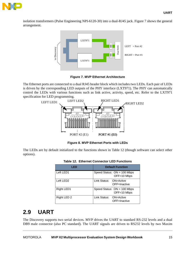
UART
isolation transformers (Pulse Engineering NPI-6120-30) into a dual-RJ45 jack. Figure 7 shows the generalarrangement.
Figure 7. MVP Ethernet Architecture
The Ethernet ports are connected to a dual RJ45 header block which includes two LEDs. Each pair of LEDsis driven by the corresponding LED outputs of the PHY interface (LXT971). The PHY can automaticallycontrol the LEDs with various functions such as link active, activity, speed, etc. Refer to the LXT971specification for LED programming.
Figure 8. MVP Ethernet Ports with LEDs
The LEDs are by default initialized to the functions shown in Table 12 (though software can select otheroptions).
2.9 UARTThe Discovery supports two serial devices. MVP drives the UART to standard RS-232 levels and a dualDB9 male connector (also PC standard). The UART signals are driven to RS232 levels by two Maxim
Table 12. Ethernet Connector LED Functions
LED Default Function
Left LED1 Speed Status: ON = 100 Mbps OFF=10 Mbps
Left LED2 Link Status: ON=ActiveOFF=Inactive
Right LED1 Speed Status: ON = 100 MbpsOFF=10 Mbps
Right LED 2 Link Status: ON=ActiveOFF=Inactive
LXT971
to D
isco
very
LXT971
Dua
l RJ4
5 LEFT = Port #2
RIGHT = Port #1
RIGHT LED1RIGHT LED2
LEFT LED2LEFT LED1
PORT #1 (E0)PORT #1 (E0)PORT #2 (E1)
MOTOROLA MVP X2 Multiprocessor Evaluation System Design Workbook 15

I2C
MAX211CAI chips, which also provide ESD protection to the ports with no additional circuitry. Table 13.shows the location and use of each port.
These serial ports are standard DTE (Data Terminal Equipment) ports, so to connect MVP to anothercomputer (for terminal emulator purposes) requires a “null-modem” cable. Refer to the DINK User’sManual for details on such a cable, if needed.
2.10 I2CMVP uses an I2C bus to communicate with various on-board peripherals. The I2C controller is provided inthe Discovery device. Table 14 describes the address at which each device may be found.
For details on the internal registers of the LM87, or on the format of DIMM SPD data, refer to thecorresponding document in Table 36..
2.11 PIPCThe PCI Integrated Peripheral Controller (PIPC), also referred to as SIO on MVP, contains numerous I/Oand control facilities needed for modern computer systems or embedded OS support, including:
• Dual UltraDMA-33 IDE disk interface
• Dual USB interface
• PS2 Keyboard and Mouse interface
• NVRAM
• APC power controller
• Secondary PCI interrupt controller
The SIO used on MVP is the Via Technologies VT82C586B. This SIO is used on many PC motherboard,so OS support should be relatively straightforward and many drivers may already exist for SIO functions.The SIO also includes an PCI interrupt controller which may be used to re-architect the interrupt hierarchiesof MVP. Refer to the interrupt architecture section for more detail on the use of the VIA SIO PCI interruptin this manner.
Table 13. UART Information
UART Location Function
0 Top DINK Console
1 Bottom DINK Host
Table 14. I2C Addresses
Address Device Description
0x4D LM87 System Monitor
0x50 SDRAM DIMM #1 DIMM SPD Information
0x51 SDRAM DIMM #2 DIMM SPD Information
0x57 EEPROM 256 bytes of general-purpose storage
16 MVP X2 Multiprocessor Evaluation System Design Workbook MOTOROLA
PIPC
2.11.1 IDEThe SIO has a PC-compatible dual-channel UltraDMA-33 IDE disk controller. Interrupts flow through theVIA PCI interrupt controller (which must be used whether the VIA PCI interrupt controller is used for otherpurposes or not) into the dedicated SIOINT interrupt pin to the Discovery.
2.11.2 PS/2The SIO has a dual PS/2 driver which can be used to connect PS/2-style keyboard and mice.
The interface is identical to that used on PCs; once the VIA has been programmed as a valid PCI target forI/O accesses, the PS/2 interface may be controlled at standard PC addresses (i.e. XX00_0060/XX00_0064,where “XX” is software-determined).
2.11.3 USBThe SIO includes two USB 1.0/UHCI-1.1 compatible ports for connecting to keyboards, mice, scanners,printers, and other peripherals. MVP has an internal power supply capable of supplying up to 500mA to eachUSB device, and short-circuit protection at 1.25A.
2.11.4 NVRAMThe SIO has 256 bytes of battery-backed (NV) RAM. The SIO maintains the state of the NVRAM usingeither the VSTBY power available from the ATX power supply when it is plugged in (but not necessarily“ON”), or from the lithium coin cell on the motherboard.
2.11.5 APCThe SIO contains an APC power controller which allows “soft” power supply on-off via front-panelswitches, by timers in the APC, or by software. The APC also manages transitions between standby powerand the 3V coin-cell battery in maintaining the contents of the RTC and NVRAM.
Table 15. PS/2 Port Location
Location Function
Top PS/2 Mouse
Bottom PS/2 Keyboard
MOTOROLA MVP X2 Multiprocessor Evaluation System Design Workbook 17
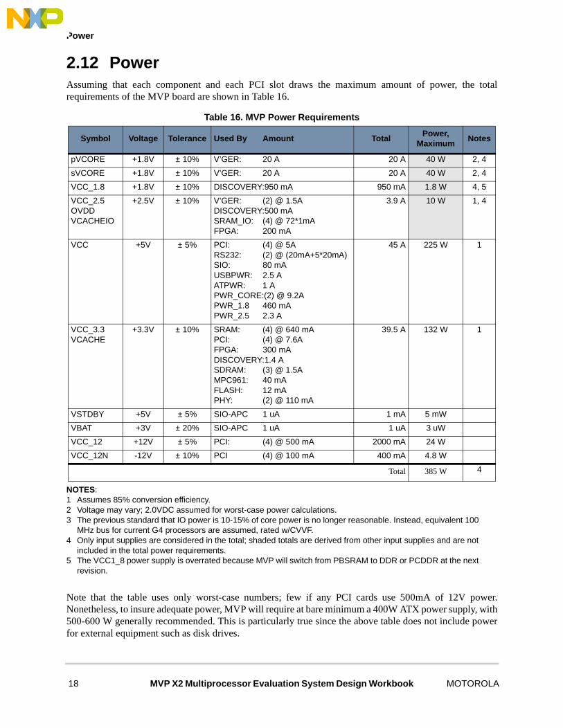
Power
2.12 PowerAssuming that each component and each PCI slot draws the maximum amount of power, the totalrequirements of the MVP board are shown in Table 16.
NOTES:1 Assumes 85% conversion efficiency.2 Voltage may vary; 2.0VDC assumed for worst-case power calculations.3 The previous standard that IO power is 10-15% of core power is no longer reasonable. Instead, equivalent 100
MHz bus for current G4 processors are assumed, rated w/CVVF.4 Only input supplies are considered in the total; shaded totals are derived from other input supplies and are not
included in the total power requirements.5 The VCC1_8 power supply is overrated because MVP will switch from PBSRAM to DDR or PCDDR at the next
revision.
Note that the table uses only worst-case numbers; few if any PCI cards use 500mA of 12V power.Nonetheless, to insure adequate power, MVP will require at bare minimum a 400W ATX power supply, with500-600 W generally recommended. This is particularly true since the above table does not include powerfor external equipment such as disk drives.
Table 16. MVP Power Requirements
Symbol Voltage Tolerance Used By Amount TotalPower,
MaximumNotes
pVCORE +1.8V ± 10% V’GER: 20 A 20 A 40 W 2, 4
sVCORE +1.8V ± 10% V’GER: 20 A 20 A 40 W 2, 4
VCC_1.8 +1.8V ± 10% DISCOVERY:950 mA 950 mA 1.8 W 4, 5
VCC_2.5OVDDVCACHEIO
+2.5V ± 10% V’GER: (2) @ 1.5ADISCOVERY:500 mASRAM_IO: (4) @ 72*1mAFPGA: 200 mA
3.9 A 10 W 1, 4
VCC +5V ± 5% PCI: (4) @ 5ARS232: (2) @ (20mA+5*20mA)SIO: 80 mAUSBPWR: 2.5 AATPWR: 1 APWR_CORE:(2) @ 9.2APWR_1.8 460 mAPWR_2.5 2.3 A
45 A 225 W 1
VCC_3.3VCACHE
+3.3V ± 10% SRAM: (4) @ 640 mAPCI: (4) @ 7.6AFPGA: 300 mADISCOVERY:1.4 ASDRAM: (3) @ 1.5AMPC961: 40 mAFLASH: 12 mAPHY: (2) @ 110 mA
39.5 A 132 W 1
VSTDBY +5V ± 5% SIO-APC 1 uA 1 mA 5 mW
VBAT +3V ± 20% SIO-APC 1 uA 1 uA 3 uW
VCC_12 +12V ± 5% PCI: (4) @ 500 mA 2000 mA 24 W
VCC_12N -12V ± 10% PCI (4) @ 100 mA 400 mA 4.8 W
Total 385 W 4
18 MVP X2 Multiprocessor Evaluation System Design Workbook MOTOROLA

Interrupts
Standard ATX power supplies are available in this range. Table 17. lists some compatible power supplies.
2.13 InterruptsMVP uses the Discovery as a the primary interrupt handler, and optionally can relegate some interrupts tothe Via SuperIO. Discovery has an extensive interrupt flexibilities, but it is somewhat limited in the numberof discrete interrupts supported. Furthermore, the interrupt controller is quite different from that of theMPC107/MPC8240 EPIC or PC PIC, so software may require some careful thought in this area.
The MVP interrupt architecture is shown in Figure 9.
Figure 9. MVP Interrupt Architecture
There are many external interrupt sources possible on an MVP platform, in addition to the numerous onesavailable inside Discovery (including but not limited to ethernet, serial, DMA, PCI handling, and memoryerrors). Since Discovery has a limited number of directly triggerable interrupt input pins (basicallyinterrupts are triggered on one of the four MPP byte lanes), interrupt handlers will have to essentially share
Table 17. MVP Power Supply Vendors
Manufacturer Part Number Power Contact
Sparkle Power FSP400-60PFN(12V) 400W www.sparklepower.com
DISCOVERY
CPU #1
MPP
7-0
MPP
15-8
MPP
23-1
6M
PP31
-24 CPU #2
CPUINTInterruptSteering
PCI0INTInterruptSteering
PCI1INTInterruptSteering
unused
SIO
primaryPCI
secondaryPCI
PHYsEthernet
MOTOROLA MVP X2 Multiprocessor Evaluation System Design Workbook 19

Interrupts
interrupts. The SuperIO PIC can be used to handle the secondary PCI bus interrupt for a reduction ininterrupt sharing, though an additional level of interrupt processing hierarchy is introduced.
Discovery has one primary CPUINT signal, which is used to signal CPU #1 (Primary). For the second CPU,the secondary PCI interrupt output PCI1INT is used. Despite the name, these interrupts have the samecapabilities as the CPUINT signal, so once any of the interrupt sources have been routed as shown inTable 18, it may be further routed to a particular processor.
NOTES:1 Requires MPP setup.2 Interrupts are shared in a rotating fashion among PCI domains to handle multi-interrupt-capable boards.3 An active-high/edge-triggered interrupt, unlike PCI interrupt drivers (active-low/level-sensitive).
Note that all of the external interrupt resources are connected through the MPP port, so MPP setup isrequired for any interrupts.
Since the Discovery cannot trigger a distinct interrupt on the change of one MPP pin, as noted aboveinterrupt handling software must be prepared to poll or otherwise handle the possibility that one or all of thedevices on a single MPP byte lane are asserting interrupts. For example, an interrupt from MPP byte lane 1could be caused by:
• primary PCI slot 1 INTC#/INTD# pins (fairly rare)
• primary PCI slot 2 INTB#/INTC# pins (fairly rare)
• secondary PCI slot 1 INT(A:D)# pins (fairly likely)
Table 18. MVP Interrupt Resources
Interrupt ConnectionMPP Byte
LaneDriving Resource(s) Notes
PCI Error (internal) N/A (internal)
N/A
Cross-processor 1->0 MPP bit #4 0 MPP[31]
Primary PCI Int0 MPP bit #6 0 pSLOT_INT(1)-INTA#pSLOT_INT(2)-INTD#
1, 2
Primary PCI Int1 MPP bit #7 0 pSLOT_INT(1)-INTB#pSLOT_INT(2)-INTA#
1, 2
Primary PCI Int2 MPP bit #8 1 pSLOT_INT(1)-INTC#pSLOT_INT(2)-INTB#
1, 2
Primary PCI Int3 MPP bit #9 1 pSLOT_INT(1)-INTD#pSLOT_INT(2)-INTC#
1, 2
Secondary PCI Int0 MPP bit #10 1 sSLOT_INT(1)-INTA#sSLOT_INT(2)-INTD#
1, 2
Secondary PCI Int1 MPP bit #11 1 sSLOT_INT(1)-INTB#sSLOT_INT(2)-INTA#
1, 2
Secondary PCI Int2 MPP bit #12 1 sSLOT_INT(1)-INTC#sSLOT_INT(2)-INTB#
1, 2
Secondary PCI Int3 MPP bit #13 1 sSLOT_INT(1)-INTD#sSLOT_INT(2)-INTC#
1, 2
ENet PHY #1 Interrupt MPP bit #14 1 LXT971A #1(L) MDINT*
ENet PHY #2 Interrupt MPP bit #15 1 LXT971A #2(R) MDINT*
SuperIO Interrupt MPP bit #22 2 SIOINT 3
Cross-processor 0->1 MPP bit #30 3 MPP[5]
20 MVP X2 Multiprocessor Evaluation System Design Workbook MOTOROLA

Interrupts
• secondary PCI slot 2 INT(A:D)# pins (fairly likely)
• ethernet PHY interrupts (1 and 2) (possible)
2.13.1 Cross-Processor InterruptsA common requirement for multiprocessing systems is to allow one CPU to interrupt another, referred to asa cross-processor interrupt. This facility may be used to allow one CPU to hand off interrupt processing toanother, or to perform dynamic load balancing of processes.
Since the Discovery does not include a special path for cross-processor interrupts, MVP uses a combinationof general-purpose software controlled outputs (GPIO ports), and general-purpose interrupt inputs. Thesefunctions are all available through the MPP port of Discovery with appropriate programming.
The cross-processor interrupt architecture is shown in Figure 10.
Figure 10. Cross-Processor Interrupts
To use the cross-processor facility, the initialization software must set and use the MPP ports as describedin see “MVP Cross-Processor Interrupts” on page 21..
Table 19. MVP Cross-Processor Interrupts
ActionIntiialization
ActorOutput Setup Interrupt Setup Assert Action Interrupt Action
Byte Lane
CPU 1 -> CPU 2
CPU #1 Set MPP bit 5 to output.
Set MPP bit 5 = 0,Set MPP bit 5 = 1.
0
CPU #2 Set MPP bit 30 to:active-lowedge-triggeredinterrupt.
OS-dependant 3
DISCOVERY
5
CPU #1
MPP
7-0
MPP
15-8
MPP
23-1
6M
PP31
-24
4
30
31
CPU #2
CPUINTInterruptSteering
PCI0INTInterruptSteering
PCI1INTInterruptSteering
MOTOROLA MVP X2 Multiprocessor Evaluation System Design Workbook 21
Reset
Notice that in the table, CPU1 only uses byte lane 0 (aligned at 0xF100_XXX0) while CPU2 uses only bytelane 3 (aligned at 0xF100_XXX3). Since Discovery allows byte-access to the MPP control/status bits,processors can read from or write to the associated byte portion of the 32-bit MPP ports without requiringlocks or semaphores for shared arbitration, as is otherwise often needed.
2.13.2 PCI Secondary PCI Interrupt HandlingAs noted in Section 2.2.1 earlier, the VIA PIPC can serve as a secondary PCI interrupt handler, merging theinterrupt sources from the two secondary PCI slots with its own interrupt capabilities (IDE, USB, serial,PS/2) to the standard SIOINT pin. This allows modelling software which requires the presence of an 8259PIC.
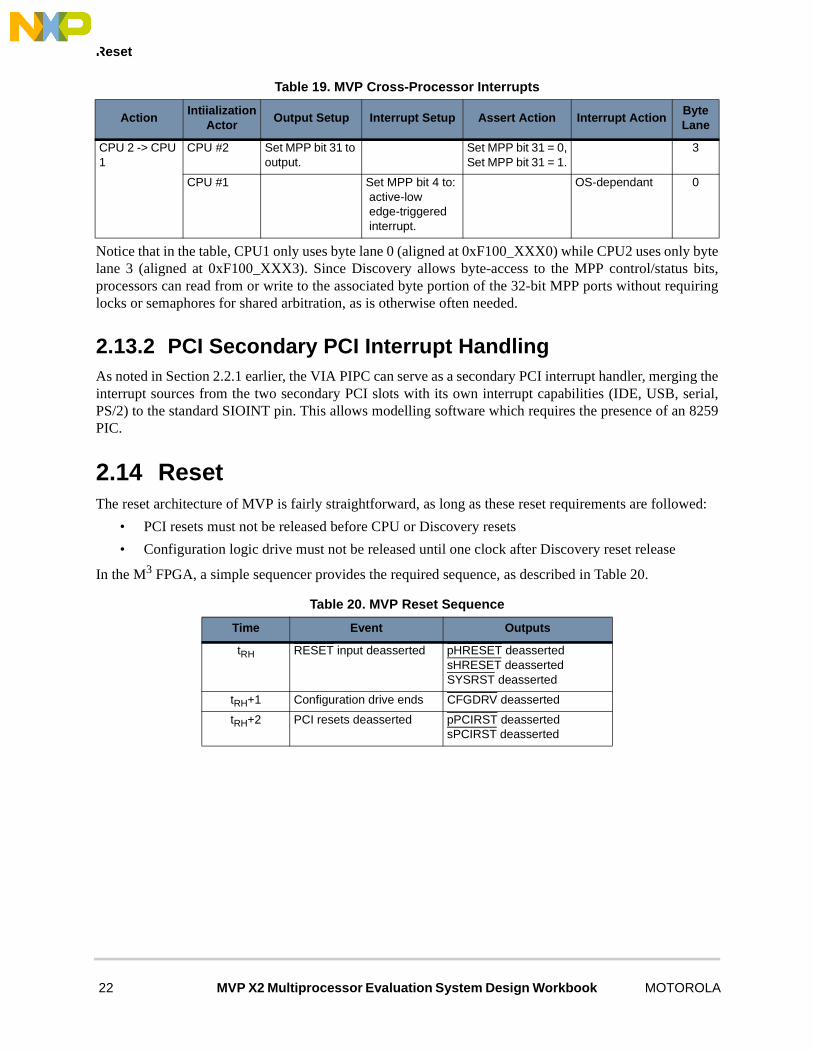
2.14 ResetThe reset architecture of MVP is fairly straightforward, as long as these reset requirements are followed:
• PCI resets must not be released before CPU or Discovery resets
• Configuration logic drive must not be released until one clock after Discovery reset release
In the M3 FPGA, a simple sequencer provides the required sequence, as described in Table 20.
CPU 2 -> CPU 1
CPU #2 Set MPP bit 31 to output.
Set MPP bit 31 = 0,Set MPP bit 31 = 1.
3
CPU #1 Set MPP bit 4 to:active-lowedge-triggeredinterrupt.
OS-dependant 0
Table 20. MVP Reset Sequence
Time Event Outputs
tRH RESET input deasserted pHRESET deassertedsHRESET deassertedSYSRST deasserted
tRH+1 Configuration drive ends CFGDRV deasserted
tRH+2 PCI resets deasserted pPCIRST deassertedsPCIRST deasserted
Table 19. MVP Cross-Processor Interrupts
ActionIntiialization
ActorOutput Setup Interrupt Setup Assert Action Interrupt Action
Byte Lane
22 MVP X2 Multiprocessor Evaluation System Design Workbook MOTOROLA

Reset
The general reset architecture is shown in Figure 11.
Figure 11. MVP Reset Architecture
In operation, the ATX power supply or either of the reset pushbutton switches may initiate a system resetand cause the reset controller to drive the global reset signal RESET low. The FPGA, in turn, derives thesecondary reset signals and drives them at the appropriate time.
The reset controller keeps RESET asserted for approximately 350 milliseconds, which is sufficient to resetall Motorola MPC745X processors as well as others used on MVP. Upon release, the Discovery controllerlatches in configuration options, and then begins to process bus transaction.
2.14.1 Service InterruptMVP includes a debounced reset switch which can be configured to assert one of the signals in Table 21..
NOTES:1 Default as shipped.2 All other resistors should generally be removed except the signal of interest.
Note that changing the assertion selection requires moving a 0-Ω resistor.
Table 21. Service Switch Definition
DefinitionAsserted
SignalInstall Note
Primary CPU Soft-Reset pSRESET R271 1, 2
Secondary CPU Soft-Reset sSRESET R265 2
Primary CPU Checkstop pCKSTPI R266 2
Secondary CPU Checkstop sCKSTPI R267 2
Primary Machine Check pMCP R268 2
Primary Service Management Interrupt pSMI R269 2
PHY
IDE
FLASH
SMON
RSTCTL
M3
COPDISCO.
SIO
pPCI
sPCI
pCPU
sCPU
ATXPWR
RSTSWITCH
RCtl
MOTOROLA MVP X2 Multiprocessor Evaluation System Design Workbook 23
Diagnostic Functions
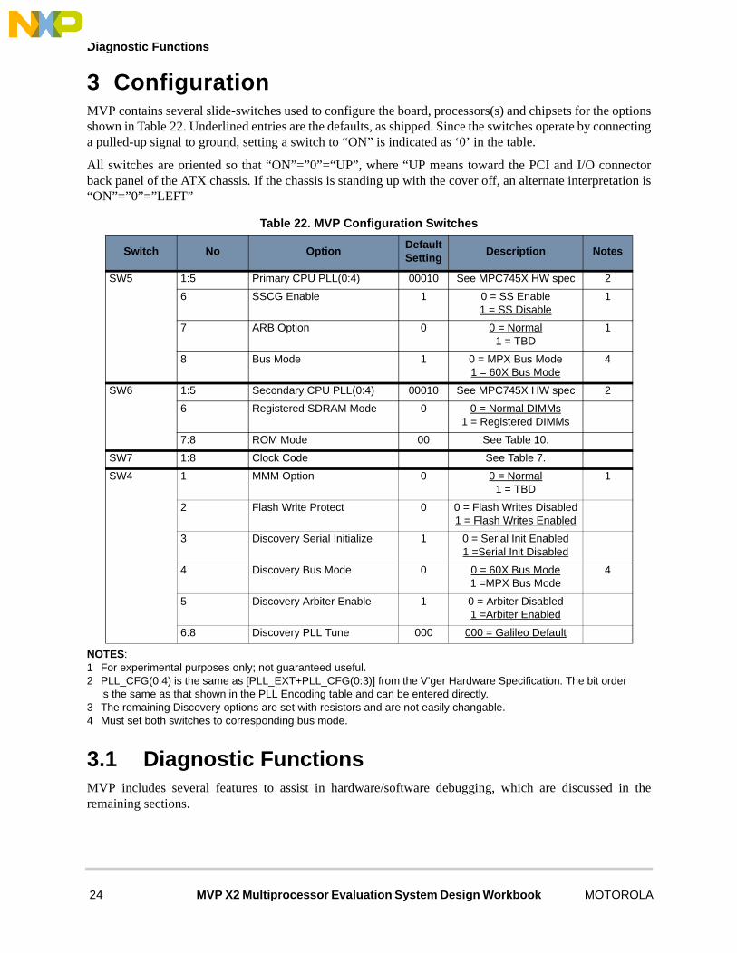
3 ConfigurationMVP contains several slide-switches used to configure the board, processors(s) and chipsets for the optionsshown in Table 22. Underlined entries are the defaults, as shipped. Since the switches operate by connectinga pulled-up signal to ground, setting a switch to “ON” is indicated as ‘0’ in the table.
All switches are oriented so that “ON”=”0”=“UP”, where “UP means toward the PCI and I/O connectorback panel of the ATX chassis. If the chassis is standing up with the cover off, an alternate interpretation is“ON”=”0”=”LEFT”
NOTES:1 For experimental purposes only; not guaranteed useful.2 PLL_CFG(0:4) is the same as [PLL_EXT+PLL_CFG(0:3)] from the V’ger Hardware Specification. The bit order
is the same as that shown in the PLL Encoding table and can be entered directly.3 The remaining Discovery options are set with resistors and are not easily changable.4 Must set both switches to corresponding bus mode.
3.1 Diagnostic FunctionsMVP includes several features to assist in hardware/software debugging, which are discussed in theremaining sections.
Table 22. MVP Configuration Switches
Switch No OptionDefault Setting
Description Notes
SW5 1:5 Primary CPU PLL(0:4) 00010 See MPC745X HW spec 2
6 SSCG Enable 1 0 = SS Enable1 = SS Disable
1
7 ARB Option 0 0 = Normal1 = TBD
1
8 Bus Mode 1 0 = MPX Bus Mode1 = 60X Bus Mode
4
SW6 1:5 Secondary CPU PLL(0:4) 00010 See MPC745X HW spec 2
6 Registered SDRAM Mode 0 0 = Normal DIMMs1 = Registered DIMMs
7:8 ROM Mode 00 See Table 10.
SW7 1:8 Clock Code See Table 7.
SW4 1 MMM Option 0 0 = Normal1 = TBD
1
2 Flash Write Protect 0 0 = Flash Writes Disabled1 = Flash Writes Enabled
3 Discovery Serial Initialize 1 0 = Serial Init Enabled1 =Serial Init Disabled
4 Discovery Bus Mode 0 0 = 60X Bus Mode1 =MPX Bus Mode
4
5 Discovery Arbiter Enable 1 0 = Arbiter Disabled1 =Arbiter Enabled
6:8 Discovery PLL Tune 000 000 = Galileo Default
24 MVP X2 Multiprocessor Evaluation System Design Workbook MOTOROLA
Diagnostic Functions
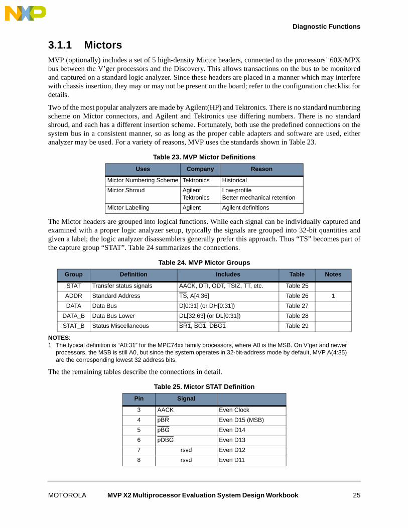
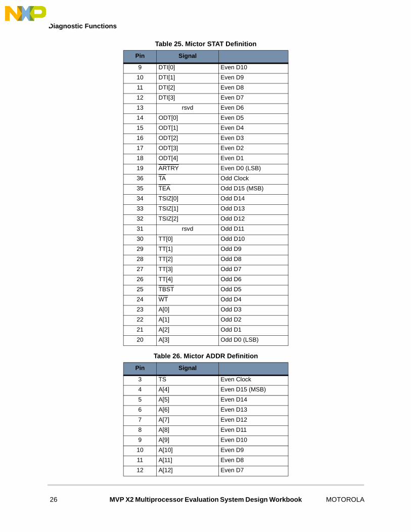
3.1.1 MictorsMVP (optionally) includes a set of 5 high-density Mictor headers, connected to the processors’ 60X/MPXbus between the V’ger processors and the Discovery. This allows transactions on the bus to be monitoredand captured on a standard logic analyzer. Since these headers are placed in a manner which may interferewith chassis insertion, they may or may not be present on the board; refer to the configuration checklist fordetails.
Two of the most popular analyzers are made by Agilent(HP) and Tektronics. There is no standard numberingscheme on Mictor connectors, and Agilent and Tektronics use differing numbers. There is no standardshroud, and each has a different insertion scheme. Fortunately, both use the predefined connections on thesystem bus in a consistent manner, so as long as the proper cable adapters and software are used, eitheranalyzer may be used. For a variety of reasons, MVP uses the standards shown in Table 23.
The Mictor headers are grouped into logical functions. While each signal can be individually captured andexamined with a proper logic analyzer setup, typically the signals are grouped into 32-bit quantities andgiven a label; the logic analyzer disassemblers generally prefer this approach. Thus “TS” becomes part ofthe capture group “STAT”. Table 24 summarizes the connections.
NOTES:1 The typical definition is “A0:31” for the MPC74xx family processors, where A0 is the MSB. On V’ger and newer
processors, the MSB is still A0, but since the system operates in 32-bit-address mode by default, MVP A(4:35) are the corresponding lowest 32 address bits.
The the remaining tables describe the connections in detail.
Table 23. MVP Mictor Definitions
Uses Company Reason
Mictor Numbering Scheme Tektronics Historical
Mictor Shroud AgilentTektronics
Low-profileBetter mechanical retention
Mictor Labelling Agilent Agilent definitions
Table 24. MVP Mictor Groups
Group Definition Includes Table Notes
STAT Transfer status signals AACK, DTI, ODT, TSIZ, TT, etc. Table 25
ADDR Standard Address TS, A[4:36] Table 26 1
DATA Data Bus D[0:31] (or DH[0:31]) Table 27
DATA_B Data Bus Lower DL[32:63] (or DL[0:31]) Table 28
STAT_B Status Miscellaneous BR1, BG1, DBG1 Table 29
Table 25. Mictor STAT Definition
Pin Signal
3 AACK Even Clock
4 pBR Even D15 (MSB)
5 pBG Even D14
6 pDBG Even D13
7 rsvd Even D12
8 rsvd Even D11
MOTOROLA MVP X2 Multiprocessor Evaluation System Design Workbook 25
Diagnostic Functions
9 DTI[0] Even D10
10 DTI[1] Even D9
11 DTI[2] Even D8
12 DTI[3] Even D7
13 rsvd Even D6
14 ODT[0] Even D5
15 ODT[1] Even D4
16 ODT[2] Even D3
17 ODT[3] Even D2
18 ODT[4] Even D1
19 ARTRY Even D0 (LSB)
36 TA Odd Clock
35 TEA Odd D15 (MSB)
34 TSIZ[0] Odd D14
33 TSIZ[1] Odd D13
32 TSIZ[2] Odd D12
31 rsvd Odd D11
30 TT[0] Odd D10
29 TT[1] Odd D9
28 TT[2] Odd D8
27 TT[3] Odd D7
26 TT[4] Odd D6
25 TBST Odd D5
24 WT Odd D4
23 A[0] Odd D3
22 A[1] Odd D2
21 A[2] Odd D1
20 A[3] Odd D0 (LSB)
Table 26. Mictor ADDR Definition
Pin Signal
3 TS Even Clock
4 A[4] Even D15 (MSB)
5 A[5] Even D14
6 A[6] Even D13
7 A[7] Even D12
8 A[8] Even D11
9 A[9] Even D10
10 A[10] Even D9
11 A[11] Even D8
12 A[12] Even D7
Table 25. Mictor STAT Definition
Pin Signal
26 MVP X2 Multiprocessor Evaluation System Design Workbook MOTOROLA

Diagnostic Functions
13 A[13] Even D6
14 A[14] Even D5
15 A[15] Even D4
16 A[16] Even D3
17 A[17] Even D2
18 A[18] Even D1
19 A[19] Even D0 (LSB)
36 LACLK Odd Clock
35 A[20] Odd D15 (MSB)
34 A[21] Odd D14
33 A[22] Odd D13
32 A[23] Odd D12
31 A[24] Odd D11
30 A[25] Odd D10
29 A[26] Odd D9
28 A[27] Odd D8
27 A[28] Odd D7
26 A[29] Odd D6
25 A[30] Odd D5
24 A[31] Odd D4
23 A[32] Odd D3
22 A[33] Odd D2
21 A[34] Odd D1
20 A[35] Odd D0 (LSB)
Table 27. Mictor DATA Definition
Pin Signal
3 rsvd Even Clock
4 D[0] Even D15 (MSB)
5 D[1] Even D14
6 D[2] Even D13
7 D[3] Even D12
8 D[4] Even D11
9 D[5] Even D10
10 D[6] Even D9
11 D[7] Even D8
12 D[8] Even D7
13 D[9] Even D6
14 D[10] Even D5
15 D[11] Even D4
16 D[12] Even D3
Table 26. Mictor ADDR Definition
Pin Signal
MOTOROLA MVP X2 Multiprocessor Evaluation System Design Workbook 27

Diagnostic Functions
17 D[13] Even D2
18 D[14] Even D1
19 D[15] Even D0 (LSB)
36 rsvd Odd Clock
35 D[16] Odd D15 (MSB)
34 D[17] Odd D14
33 D[18] Odd D13
32 D[19] Odd D12
31 D[20] Odd D11
30 D[21] Odd D10
29 D[22] Odd D9
28 D[23] Odd D8
27 D[24] Odd D7
26 D[25] Odd D6
25 D[26] Odd D5
24 D[27] Odd D4
23 D[28] Odd D3
22 D[29] Odd D2
21 D[30] Odd D1
20 D[31] Odd D0 (LSB)
Table 28. Mictor DATA_B Definition
Pin Signal
3 rsvd Even Clock
4 D[32] Even D15 (MSB)
5 D[33] Even D14
6 D[34] Even D13
7 D[35] Even D12
8 D[36] Even D11
9 D[37] Even D10
10 D[38] Even D9
11 D[39] Even D8
12 D[40] Even D7
13 D[41] Even D6
14 D[42] Even D5
15 D[43] Even D4
16 D[44] Even D3
17 D[45] Even D2
18 D[46] Even D1
19 D[47] Even D0 (LSB)
36 rsvd Odd Clock
Table 27. Mictor DATA Definition
Pin Signal
28 MVP X2 Multiprocessor Evaluation System Design Workbook MOTOROLA

Diagnostic Functions
35 D[48] Odd D15 (MSB)
34 D[49] Odd D14
33 D[50] Odd D13
32 D[51] Odd D12
31 D[52] Odd D11
30 D[53] Odd D10
29 D[54] Odd D9
28 D[55] Odd D8
27 D[56] Odd D7
26 D[57] Odd D6
25 D[58] Odd D5
24 D[59] Odd D4
23 D[60] Odd D3
22 D[61] Odd D2
21 D[62] Odd D1
20 D[63] Odd D0 (LSB)
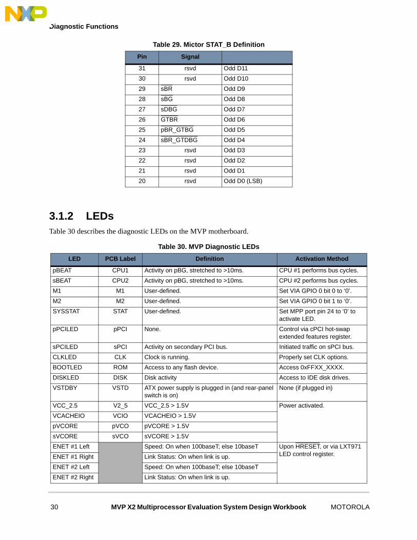
Table 29. Mictor STAT_B Definition
Pin Signal
3 rsvd Even Clock
4 pINT Even D15 (MSB)
5 sINT Even D14
6 pCPU_HRST Even D13
7 rsvd Even D12
8 rsvd Even D11
9 rsvd Even D10
10 rsvd Even D9
11 rsvd Even D8
12 rsvd Even D7
13 rsvd Even D6
14 rsvd Even D5
15 rsvd Even D4
16 rsvd Even D3
17 rsvd Even D2
18 rsvd Even D1
19 rsvd Even D0 (LSB)
36 rsvd Odd Clock
35 F1VIS Odd D15 (MSB)
34 F2VIS Odd D14
33 rsvd Odd D13
32 rsvd Odd D12
Table 28. Mictor DATA_B Definition
Pin Signal
MOTOROLA MVP X2 Multiprocessor Evaluation System Design Workbook 29
Diagnostic Functions
3.1.2 LEDsTable 30 describes the diagnostic LEDs on the MVP motherboard.
31 rsvd Odd D11
30 rsvd Odd D10
29 sBR Odd D9
28 sBG Odd D8
27 sDBG Odd D7
26 GTBR Odd D6
25 pBR_GTBG Odd D5
24 sBR_GTDBG Odd D4
23 rsvd Odd D3
22 rsvd Odd D2
21 rsvd Odd D1
20 rsvd Odd D0 (LSB)
Table 30. MVP Diagnostic LEDs
LED PCB Label Definition Activation Method
pBEAT CPU1 Activity on pBG, stretched to >10ms. CPU #1 performs bus cycles.
sBEAT CPU2 Activity on pBG, stretched to >10ms. CPU #2 performs bus cycles.
M1 M1 User-defined. Set VIA GPIO 0 bit 0 to ‘0’.
M2 M2 User-defined. Set VIA GPIO 0 bit 1 to ‘0’.
SYSSTAT STAT User-defined. Set MPP port pin 24 to ‘0’ to activate LED.
pPCILED pPCI None. Control via cPCI hot-swap extended features register.
sPCILED sPCI Activity on secondary PCI bus. Initiated traffic on sPCI bus.
CLKLED CLK Clock is running. Properly set CLK options.
BOOTLED ROM Access to any flash device. Access 0xFFXX_XXXX.
DISKLED DISK Disk activity Access to IDE disk drives.
VSTDBY VSTD ATX power supply is plugged in (and rear-panel switch is on)
None (if plugged in)
VCC_2.5 V2_5 VCC_2.5 > 1.5V Power activated.
VCACHEIO VCIO VCACHEIO > 1.5V
pVCORE pVCO pVCORE > 1.5V
sVCORE sVCO sVCORE > 1.5V
ENET #1 Left Speed: On when 100baseT; else 10baseT Upon HRESET, or via LXT971 LED control register.ENET #1 Right Link Status: On when link is up.
ENET #2 Left Speed: On when 100baseT; else 10baseT
ENET #2 Right Link Status: On when link is up.
Table 29. Mictor STAT_B Definition
Pin Signal
30 MVP X2 Multiprocessor Evaluation System Design Workbook MOTOROLA
Diagnostic Functions
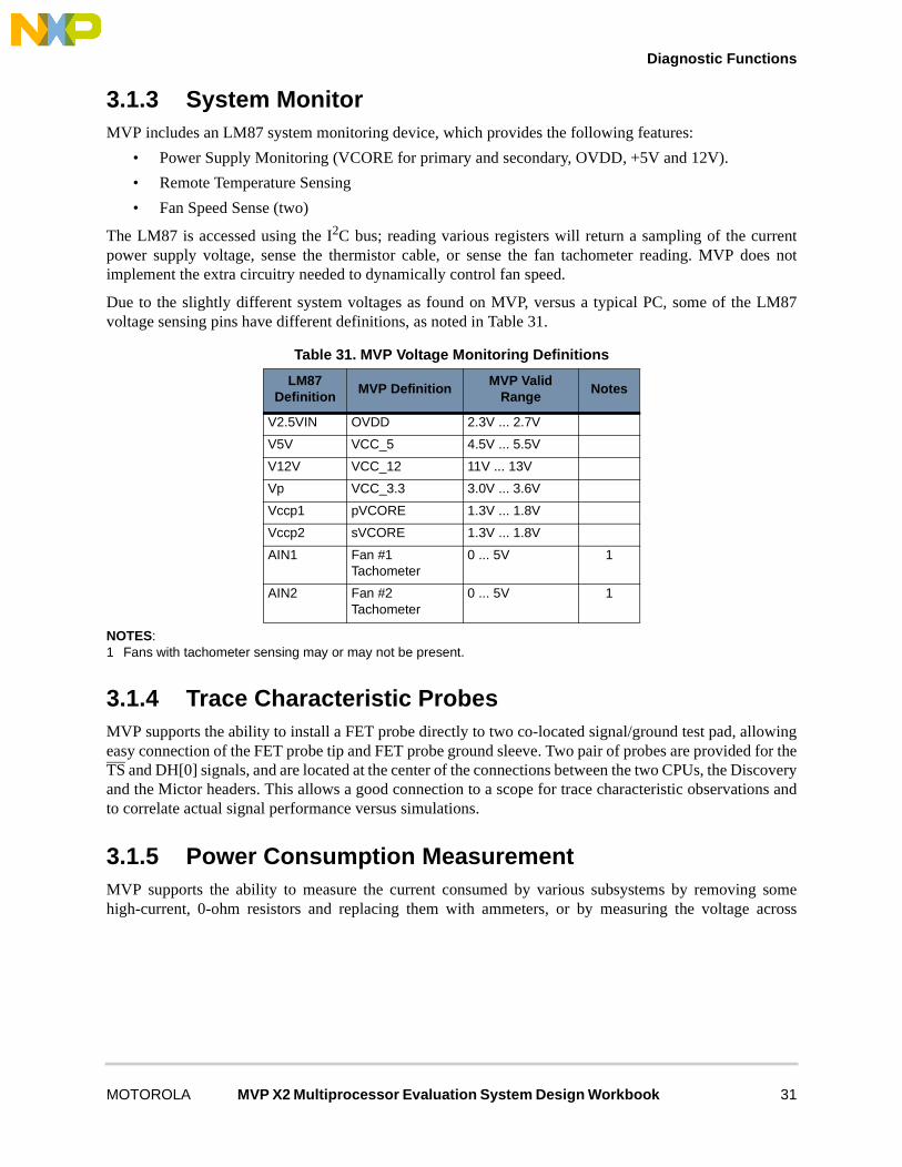
3.1.3 System MonitorMVP includes an LM87 system monitoring device, which provides the following features:
• Power Supply Monitoring (VCORE for primary and secondary, OVDD, +5V and 12V).
• Remote Temperature Sensing
• Fan Speed Sense (two)
The LM87 is accessed using the I2C bus; reading various registers will return a sampling of the currentpower supply voltage, sense the thermistor cable, or sense the fan tachometer reading. MVP does notimplement the extra circuitry needed to dynamically control fan speed.
Due to the slightly different system voltages as found on MVP, versus a typical PC, some of the LM87voltage sensing pins have different definitions, as noted in Table 31.
NOTES:1 Fans with tachometer sensing may or may not be present.
3.1.4 Trace Characteristic ProbesMVP supports the ability to install a FET probe directly to two co-located signal/ground test pad, allowingeasy connection of the FET probe tip and FET probe ground sleeve. Two pair of probes are provided for theTS and DH[0] signals, and are located at the center of the connections between the two CPUs, the Discoveryand the Mictor headers. This allows a good connection to a scope for trace characteristic observations andto correlate actual signal performance versus simulations.
3.1.5 Power Consumption MeasurementMVP supports the ability to measure the current consumed by various subsystems by removing somehigh-current, 0-ohm resistors and replacing them with ammeters, or by measuring the voltage across
Table 31. MVP Voltage Monitoring Definitions
LM87 Definition
MVP DefinitionMVP Valid
RangeNotes
V2.5VIN OVDD 2.3V ... 2.7V
V5V VCC_5 4.5V ... 5.5V
V12V VCC_12 11V ... 13V
Vp VCC_3.3 3.0V ... 3.6V
Vccp1 pVCORE 1.3V ... 1.8V
Vccp2 sVCORE 1.3V ... 1.8V
AIN1 Fan #1 Tachometer
0 ... 5V 1
AIN2 Fan #2 Tachometer
0 ... 5V 1
MOTOROLA MVP X2 Multiprocessor Evaluation System Design Workbook 31

Diagnostic Functions
low-ohm resistors and calculating the corresponding current.. Table 32 shows some of the powermeasurements possible.
NOTES:1 Replace sense resistors with a 0.010Ω 2512 resistor.2 VCC_2.5 also supplies derivative power supplies VCACHEIO and OVDD, so it can only determined by
subtracting the latter two supplies.
The other power supplies (5V, 3.3V) can be measured through the ATX power supply.
Table 32. MVP Power Measurement
VoltageSense
ResistorUsed By Measurement Method Notes
pVCORE R217 Primary CPU ICORE = V_across_R217 / 0.0028
sVCORE R218 Secondary CPU ICORE = V_across_R218 / 0.0028
VCC_1.8 R25 GT64260 Core IVCC1.8 = V_across_R25 / 0.010
OVDD R235 CPU Bus IOFPGA IO
IOVDD = V_across_R235 / 0.010 1
VCACHEIO R9 CPU Cache IOSRAM IO
IVCACHEIO = V_across_R9 / 0.010 1
VCC_2.5 R26 GT64260 CPU Bus IOFPGA Core
IVCC2.5 = (V_across_R26 / 0.010)- IOVDD - IVCACHEIO
2
32 MVP X2 Multiprocessor Evaluation System Design Workbook MOTOROLA

Diagnostic Functions
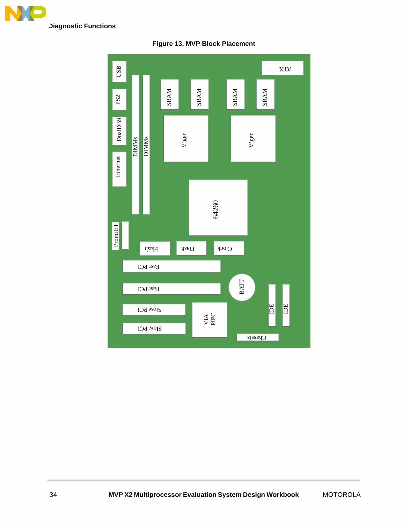
4 Placement and LayoutThe general placement of components on the MVP motherboard is shown in Figure 12.
Figure 12. MVP Placement
MOTOROLA MVP X2 Multiprocessor Evaluation System Design Workbook 33
Diagnostic Functions
Figure 13. MVP Block Placement
US
BP
S2
Dua
lDB
9E
ther
net D
IMM
s
ATX
Fast PCI
Slow PCI VIA
IDE
IDESlow PCI
Fast PCI
PIP
C
V’g
er
DIM
Ms
Chassis
BA
TT
Pro
mJE
T
V’g
er
6426
0
Flash Flash Clock
SR
AM
SR
AM
SR
AM
SR
AM
34 MVP X2 Multiprocessor Evaluation System Design Workbook MOTOROLA
Address Map
5 Programmers ModelThis section describes support information which may be useful to hardware or software designers who areusing MVP.
5.1 Address MapTable 33 shows the general address map of the MVP, while Table 34 shows the specific location of ISA/PCII/O addresses.
NOTES:1. Requires SDRAM control registers to be properly programmed (TBD).2. DINK 12.3 default; may be relocated.3. Requires software setup (CS3 registers [CS3_ADDR_LO]).4. Only software-enabled PCI/ISA I/O devices appear in this space.5. Devices may be reassigned using the ROMMODE switches. See Section 3.6. Devices default to an 8MB aperture, though 16MB is available. To get the full address range of each device, the
BOOT/DCS3 address range registers must be reprogrammed.7. Unassigned by DINK startup code; must be specified by user code.
The detailed address map in Table 34 assumes that the PnP devices have not been changed from the defaultlocations.
Table 33. Global Address Map
START END Definition Notes
0000_0000 0FFF_FFFF SDRAM 1
1E00_0000 1EFF_FFFF PCI/ISA I/O space 2
2000_XXXX 3FFF_FFFF SDRAM 1
PCI memory 7
PCI/ISA memory 7
PCI configuration address register 7
PCI configuration data register 7
Interrupt Acknowledge 7
F100_0000 F100_XXXX Discovery Configuration Registers 2
FF00_0000 FF7F_FFFF DCS3 ROM space (8MB) 3, 5, 6
FF80_0000 FFFF_FFFF Boot ROM space (8MB) 5, 6
Table 34. Detailed ISA I/O Address Map
Start End Mode Register Notes
1E00_0000 --- R/W DMA Channel 0 Base/Current Address
1E00_0001 --- R/W DMA Channel 0 Base/Current Word
1E00_0002 --- R/W DMA Channel 1 Base/Current Address
1E00_0003 --- R/W DMA Channel 1 Base/Current Word
1E00_0004 --- R/W DMA Channel 2 Base/Current Address
1E00_0005 --- R/W DMA Channel 2 Base/Current Word
1E00_0006 --- R/W DMA Channel 3 Base/Current Address
1E00_0007 --- R/W DMA Channel 3 Base/Current Word
MOTOROLA MVP X2 Multiprocessor Evaluation System Design Workbook 35

Address Map
1E00_0008 --- R DMA Controller 1 Status
W DMA Controller 1 Command
1E00_0009 --- W DMA Controller 1 Request
1E00_000A --- W DMA Controller 1 Mask
1E00_000B --- W DMA Controller 1 Mode
1E00_000C --- W DMA Controller 1 Clear Byte Pointer
1E00_000D --- W DMA Controller 1 Master Clear
1E00_000E --- W DMA Controller 1 Clear Mask
1E00_000F --- W DMA Controller 1 Write All Mask
1E00_0010 1E00_001F unassigned
1E00_0020 --- R/W PIC 1 Command
1E00_0021 --- R/W PIC 1 Command
1E00_0022 1E00_003F unassigned
1E00_0040 --- R/W Counter 0
1E00_0041 --- R/W Counter 1
1E00_0042 --- R/W Counter 2
1E00_0043 --- W Timer/Counter Control
1E00_0044 1E00_005F unassigned
1E00_0060 --- R/W Keyboard Controller Data 1
1E00_0061 --- R/W NMI Status/Control
1E00_0062 1E00_0063 unassigned
1E00_0064 --- R/W Keyboard Controller Command 1
1E00_0065 1E00_006F unassigned
1E00_0070 --- R/W RTC/APC Index 1
--- W RTC Index (shadow)
1E00_0072 --- R/W NVRAM Address
1E00_0073 --- R/W NVRAM Data
1E00_0074 1E00_0077 unassigned
1E00_0078 1E00_007F unassigned
1E00_0080 --- unassigned
1E00_0081 --- R/W DMA Memory Page 2
1E00_0082 --- R/W DMA Memory Page 3
1E00_0083 --- R/W DMA Memory Page 1
1E00_0084 FF80_0086 - DMA Reserved Page
1E00_0087 --- R/W DMA Memory Page 0
1E00_0088 --- - DMA Reserved Page
1E00_0089 --- R/W DMA Memory Page 6
1E00_008A --- R/W DMA Memory Page 7
1E00_008B --- R/W DMA Memory Page 5
1E00_008C FF80_008E - DMA Reserved Page
1E00_008F 1E00_0091 unassigned
Table 34. Detailed ISA I/O Address Map
Start End Mode Register Notes
36 MVP X2 Multiprocessor Evaluation System Design Workbook MOTOROLA

Address Map
1E00_0092 --- R/W Port 92: System Reset
1E00_0093 1E00_009F unassigned
1E00_00A0 --- R/W PIC 2 Command
1E00_00A1 --- R/W PIC 2 Command
1E00_00A2 1E00_00BF unassigned
1E00_00C0 --- R/W DMA Channel 4 Base/Current Address
1E00_00C1 --- R/W DMA Channel 4 Base/Current Word
1E00_00C2 1E00_00C3 unassigned
1E00_00C4 --- R/W DMA Channel 5 Base/Current Address
1E00_00C5 unassigned
1E00_00C6 --- R/W DMA Channel 5 Base/Current Word
1E00_00C7 unassigned
1E00_00C8 --- R/W DMA Channel 6 Base/Current Address
1E00_00C9 unassigned
1E00_00CA --- R/W DMA Channel 6 Base/Current Word
1E00_00CB unassigned
1E00_00CC --- R/W DMA Channel 7 Base/Current Address
1E00_00CD unassigned
1E00_00CE --- R/W DMA Channel 7 Base/Current Word
1E00_00CF unassigned
1E00_00D0 R DMA Controller 2 Status
"W DMA Controller 2 Command
1E00_00D3 unassigned
1E00_00D2 --- W DMA Controller 2 Request
1E00_00D3 unassigned
1E00_00D4 --- W DMA Controller 2 Mask
1E00_00D5 unassigned
1E00_00D6 --- W DMA Controller 2 Mode W
1E00_00D7 unassigned
1E00_00D8 --- W DMA Controller 2 Clear Byte Pointer
1E00_00D9 unassigned
1E00_00DA --- W DMA Controller 2 Master Clear
1E00_00DB unassigned
1E00_00DC --- W DMA Controller 2 Clear Mask
1E00_00DD unassigned
1E00_00DE --- W DMA Controller 2 Write All Mask
1E00_00DF 1E00_00FF unassigned
1E00_0100 1E00_0CF7 unassigned
1E00_0CF8 1E00_CFB R/W PCI Configuration Index Register
1E00_0CFC 1E00_CFF R/W PCI Configuration Data Register
1E00_0D00 1E00_FFFF unassigned
Table 34. Detailed ISA I/O Address Map
Start End Mode Register Notes
MOTOROLA MVP X2 Multiprocessor Evaluation System Design Workbook 37

Memory Resources
5.2 Memory ResourcesThe SIO has the following non-volatile RAM resources:
• 256 bytes of battery-backed RAM in the SIO
• 256 bytes of EEPROM in an I2C EEROM at address 0x57.
Unlike other Motorola reference design platforms such as Yellowknife or Sandpoint, MVP does not have alarge amount of storage available for environment variables, so judicious use is recommended. It is alsopossible to use the flash devices with careful software management.
38 MVP X2 Multiprocessor Evaluation System Design Workbook MOTOROLA

Initializing MVP
5.3 Initializing MVPA typical multiprocessing start-up sequence is shown in Figure 14:
Figure 14. Multiprocessing Startup Sequence
HRESET
4. Set Msg 2
2. Initialize BATs3. Initialize Cache
CPUID = ? 10
Wait Msg 1
4. Initialize 642605. Initialize SDRAM6. Setup stack pointer7. Enable IO8. Check bus speed9. Setup memory
5. Get IP from Msg6. Get MSR from Msg7. rfi
Wait Msg 2or timeout
msg2
Startup OS in multi-CPU mode.
Startup OS in multi-CPU mode.
Send code message toCPU #2 via msg1.
Enable MP Arbiter
MOTOROLA MVP X2 Multiprocessor Evaluation System Design Workbook 39
Motherboard Dimensions
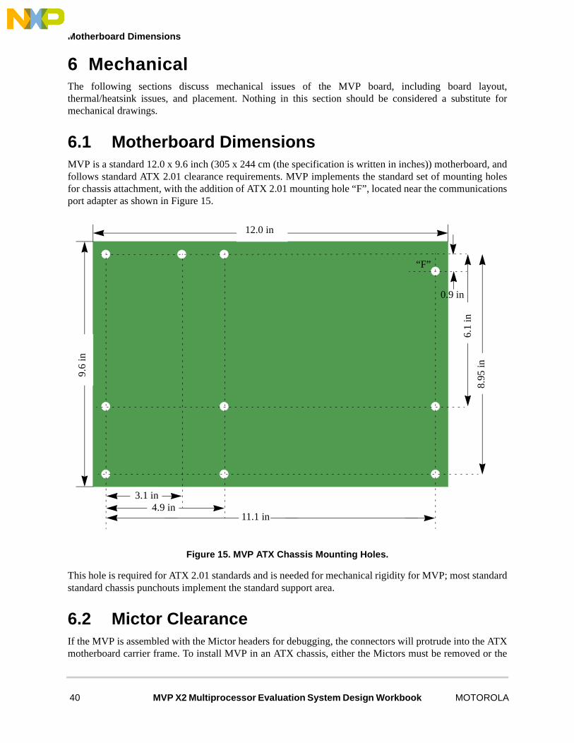
6 MechanicalThe following sections discuss mechanical issues of the MVP board, including board layout,thermal/heatsink issues, and placement. Nothing in this section should be considered a substitute formechanical drawings.
6.1 Motherboard DimensionsMVP is a standard 12.0 x 9.6 inch (305 x 244 cm (the specification is written in inches)) motherboard, andfollows standard ATX 2.01 clearance requirements. MVP implements the standard set of mounting holesfor chassis attachment, with the addition of ATX 2.01 mounting hole “F”, located near the communicationsport adapter as shown in Figure 15.
Figure 15. MVP ATX Chassis Mounting Holes.
This hole is required for ATX 2.01 standards and is needed for mechanical rigidity for MVP; most standardstandard chassis punchouts implement the standard support area.
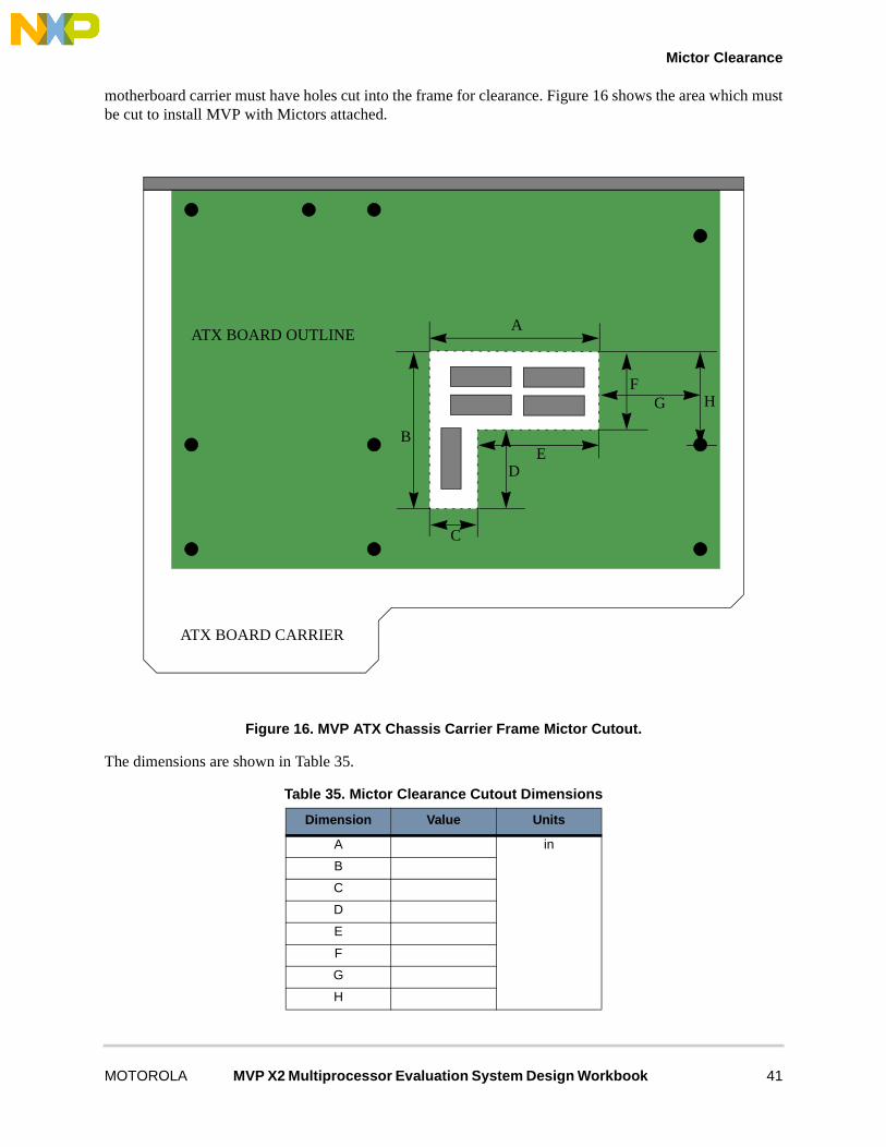
6.2 Mictor ClearanceIf the MVP is assembled with the Mictor headers for debugging, the connectors will protrude into the ATXmotherboard carrier frame. To install MVP in an ATX chassis, either the Mictors must be removed or the
12.0 in
9.6
in
4.9 in3.1 in
11.1 in
6.1
in8.
95 in
0.9 in
“F”
40 MVP X2 Multiprocessor Evaluation System Design Workbook MOTOROLA
Mictor Clearance
motherboard carrier must have holes cut into the frame for clearance. Figure 16 shows the area which mustbe cut to install MVP with Mictors attached.
Figure 16. MVP ATX Chassis Carrier Frame Mictor Cutout.
The dimensions are shown in Table 35.
Table 35. Mictor Clearance Cutout Dimensions
Dimension Value Units
A in
B
C
D
E
F
G
H
ATX BOARD OUTLINE
ATX BOARD CARRIER
A
B
C
DE
FG H
MOTOROLA MVP X2 Multiprocessor Evaluation System Design Workbook 41

ATX Chassis Gasket
Once the cutouts have been made, an MVP with Mictor headers (with or without Tektronix shrouds) can beinstalled in the carrier frame and also installed in the ATX chassis (no further clearance issues arise). Thisdoes not apply when the high-profile Agilent shrouds are used (MVP supports both styles).
6.3 ATX Chassis GasketThe particular set of IO ports provided by MVP do not match any particular ATX “gasket” (the removablepanel which fits between the motherboard and the chassis to provide EMI compliance. Because of this, theMVP will require a custom gasket, as shown in Figure 17.
Figure 17. MVP ATX Chassis Gasket
42 MVP X2 Multiprocessor Evaluation System Design Workbook MOTOROLA

Heat Sinks
7 Thermal ManagementThis section discusses some of the thermal issues related to MVP.
Do NOT operate MVP without the heatsinks and/or without the attached fan.
7.1 Heat SinksMVP uses heat sinks manufactured by Chip Coolers Inc. Refer to www.chipcoolers.com for further details.
7.2 Fan SensingIn addition to the heat sink, cooling fans are attached. MVP supports standard PC-style fan-sink speedsensors. The fans connect into a tachometry sensor in the LM87. To sense the fan speed, read thecorresponding register in the LM87 using the I2C bus.
MVP does not implement fan speed control (neither on/off nor modulation).
MOTOROLA MVP X2 Multiprocessor Evaluation System Design Workbook 43

Fan Sensing
8 Reference DocumentationTable 36 describes reference documentation which may be useful for understanding the operation of theMVP system.
Table 36. Reference Documentation
Document Number/Reference
MPC7450 Hardware Specification e-www.motorola.com/brdata/PDFDB/docs/MPC7450EC.pdf
MPC7450 User’s Manual e-www.motorola.com/brdata/PDFDB/docs/MPC7450UM.pdf
ODT e-www.motorola.com/brdata/PDFDB/docs/AN2161.pdf(also in MPC7450 hardware specification)
GD64260 (Discovery) Data Sheet www.GalileoT.com
DINK User’s Manual and code updates www.mot.com/SPS/RISC/smartnetworks/arch/
PCI 2.1 Specification www.pcisig.com
VIA 82C586B Datasheet www.via.com.tw/pdf/productinfo/586b.pdf
National LM87CIMT Datasheet www.national.com/ds/LM/LM87.pdf
SPD Serial Presence Detect Standard www.chips.ibm.com/products/memory/spddessd/spddessd.pdf
Emulations Technologies “PromJET” www.emutec.com/pjetadpt.html
LXT971 Documentation Hardware DatasheetProgramming Manual
www.level1.com
Heatsinks www.chipcoolers.com
44 MVP X2 Multiprocessor Evaluation System Design Workbook MOTOROLA

Fan Sensing
MOTOROLA MVP X2 Multiprocessor Evaluation System Design Workbook 45
xxxxxxxx/D
HOW TO REACH US:
USA/EUROPE/LOCATIONS NOT LISTED:
Motorola Literature Distribution; P.O. Box 5405, Denver, Colorado 80217 1-303-675-2140 or 1-800-441-2447
JAPAN:
Motorola Japan Ltd.; SPS, Technical Information Center, 3-20-1, Minami-Azabu Minato-ku, Tokyo 106-8573 Japan81-3-3440-3569
ASIA/PACIFIC:
Motorola Semiconductors H.K. Ltd.; Silicon Harbour Centre, 2 Dai King Street, Tai Po Industrial Estate, Tai Po, N.T., Hong Kong852-26668334
TECHNICAL INFORMATION CENTER:
1-800-521-6274
HOME PAGE:
http://www.motorola.com/semiconductors
DOCUMENT COMMENTS:
FAX (512) 933-2625, Attn: RISC Applications Engineering
Information in this document is provided solely to enable system and software implementers to use
Motorola products. There are no express or implied copyright licenses granted hereunder to design or
fabricate any integrated circuits or integrated circuits based on the information in this document.
Motorola reserves the right to make changes without further notice to any products herein. Motorola
makes no warranty, representation or guarantee regarding the suitability of its products for any
particular purpose, nor does Motorola assume any liability arising out of the application or use of any
product or circuit, and specifically disclaims any and all liability, including without limitation
consequential or incidental damages. “Typical” parameters which may be provided in Motorola data
sheets and/or specifications can and do vary in different applications and actual performance may vary
over time. All operating parameters, including “Typicals” must be validated for each customer
application by customer’s technical experts. Motorola does not convey any license under its patent
rights nor the rights of others. Motorola products are not designed, intended, or authorized for use as
components in systems intended for surgical implant into the body, or other applications intended to
support or sustain life, or for any other application in which the failure of the Motorola product could
create a situation where personal injury or death may occur. Should Buyer purchase or use Motorola
products for any such unintended or unauthorized application, Buyer shall indemnify and hold
Motorola and its officers, employees, subsidiaries, affiliates, and distributors harmless against all
claims, costs, damages, and expenses, and reasonable attorney fees arising out of, directly or
indirectly, any claim of personal injury or death associated with such unintended or unauthorized use,
even if such claim alleges that Motorola was negligent regarding the design or manufacture of the part.
Motorola and the Stylized M Logo are registered in the U.S. Patent and Trademark Office. digital dna is a trademark of Motorola, Inc. All other product or service names are the property of their respective owners. Motorola, Inc. is an Equal Opportunity/Affirmative Action Employer.
© Motorola, Inc. 2001