Design Verification and Test of Digital VLSI Circuits ... · VLSI Circuits NPTEL Video Course ....
74
Module-VII Lecture-I Introduction to Digital VLSI Testing Design Verification and Test of Digital VLSI Circuits NPTEL Video Course
Transcript of Design Verification and Test of Digital VLSI Circuits ... · VLSI Circuits NPTEL Video Course ....
Module-VII
Lecture-I
Introduction to Digital VLSI Testing
Design Verification and Test of Digital VLSI Circuits
NPTEL Video Course

Specifications
Architecture Synthesis
High Level Synthesis
RTL Design
Logic Synthesis
Physical Layout
Customer's Requirements
Manual
Front-end
Back-end
Scheduling
Allocation/Binding
Verification of RTL design with Specifications
Verification of Logic circuit with RTL Design
Verification of circuit extracted from layout with logic circuit
Floor Planning
Placement & Routing
VLSI Design, Verification and Test Flow

VLSI Design, Verification and Test Flow
Test Planning
Fabrication
Manufacturing Test
Chips to Customers

Introduction to Philosophy of Testing
• “If anything can go wrong, it will”--A very well known statement known as Murphy’s Law.
• Testing a system comprises subjecting it to inputs and checking its outputs to verify whether it behaves as per the specifications targeted during design.

Example: Electrical Iron
• Plug it in 220V AC and see if is heating. – “functional” specification, that also partially.
• Safety: – All exposed metal parts of the iron are grounded
– Auto-off on overheating
• Detailed Functionality – Heating when powered ON.
– Glowing of LED to indicate power ON.
– Temperature matching with specification for different ranges that can be set using the regulator (e.g., woolen, silk, cotton etc.)

Example: Electrical Iron
• Performance
– Power consumption as per the specifications
– Time required to reach the desired temperature when range is changed using the regulator
Tests for ONLY electrical parameters.
• Tests for mechanical parameters, like maximum height from which there is resistance to breaking of plastic parts if dropped on a tiled floor etc.
• Number of tests performed depends on the time, equipments etc. which in turn is decided by the target price of the product.
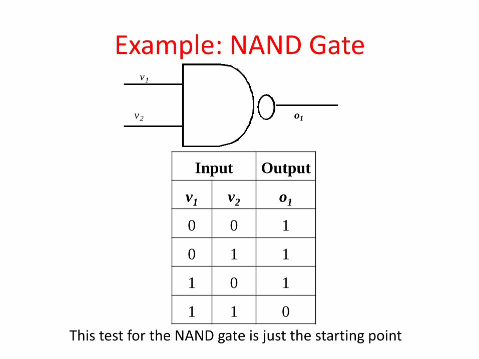
Example: NAND Gate
o1
v1
v2
Input Output
v1 v2 o1
0 0 1
0 1 1
1 0 1
1 1 0
This test for the NAND gate is just the starting point

Detailed tests for the NAND gate
• Digital Functionality
– Verify input/output of Table 1
• Delay Test
– 0 to 1: time taken by the gate to rise from 0 to 1.
• v1=1, v2=1 changed to v1=1, v2=0; After this change in input, time taken by o1 to change from 0 to 1.
• v1=1, v2=1 changed to v1=0, v2=1; After this change in input, time taken by o1 to change from 0 to 1.
• v1=1, v2=1 changed to v1=0, v2=0; After this change in input, time taken by o1 to change from 0 to 1.

Detailed tests for the NAND gate
– 1 to 0: time taken by the gate to fall from 1 to 0.
• v1=0, v2=0 changed to v1=1, v2=1; After this change in input, time taken by o1 to change from 1 to 0.
• v1=1, v2=0 changed to v1=1, v2=1; After this change in input, time taken by o1 to change from 1 to 0.
• v1=0, v2=1 changed to v1=1, v2=1; After this change in input, time taken by o1 to change from 1 to 0.
• Fan-out capability:
– Number of gates connected at o1 which can be driven by the NAND gate.
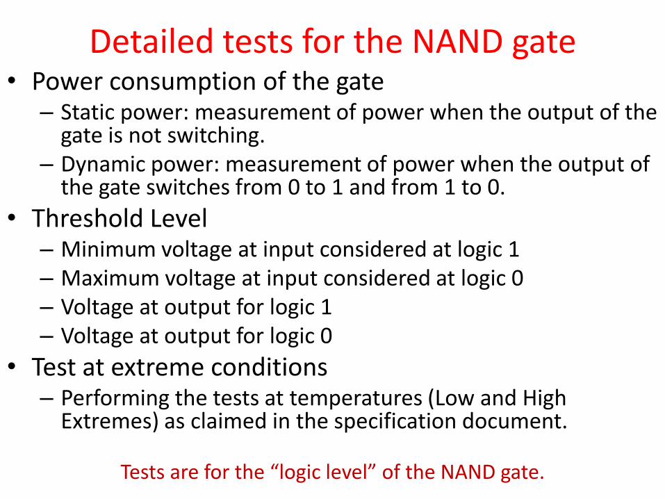
Detailed tests for the NAND gate • Power consumption of the gate
– Static power: measurement of power when the output of the gate is not switching.
– Dynamic power: measurement of power when the output of the gate switches from 0 to 1 and from 1 to 0.
• Threshold Level – Minimum voltage at input considered at logic 1 – Maximum voltage at input considered at logic 0 – Voltage at output for logic 1 – Voltage at output for logic 0
• Test at extreme conditions – Performing the tests at temperatures (Low and High
Extremes) as claimed in the specification document.
Tests are for the “logic level” of the NAND gate.

Detailed tests for the NAND gate
o1
v1
v1
v2
v1
VDD
GND
T1
T2
T3
T4
+
-
Gate
Drain
Source
Nmos (T3)
IDS
VDS
VGS
CMOS implementation for the NAND gate
VBS
Body

Detailed tests for the NAND gate • Output Characteristics
– a set of IDS vs VDS curves for different constant values of the gate-source voltage VGS
• Transfer characteristics
– a set of IDS vs VGS curves for different values of the substrate-source voltage VBS, at constant VDS
• Threshold Voltage Test
– Threshold Voltage obtained in test, matches the specifications

Detailed tests for the NAND gate
Layout of a NAND gate in a silicon die

Optimal Quality of Test
• Given a digital logic gate, what tests are to be performed to assure an acceptable quality of product at reasonable price”.
• Test for the NAND gate should be such that results are accurate (say 99% above) yet time for testing is low (less than a millisecond). – Table 1 for the NAND gate and at proper time
• DIGITAL TESTING is not testing digital circuits (comprised of logic
gates). DIGITAL TESTING is defined as testing a digital circuit to verify that it
performs the specified logic functions and in proper time.
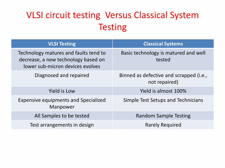
VLSI circuit testing Versus Classical System Testing
VLSI Testing Classical Systems
Technology matures and faults tend to decrease, a new technology based on
lower sub-micron devices evolves
Basic technology is matured and well tested
Diagnosed and repaired Binned as defective and scrapped (i.e., not repaired)
Yield is Low Yield is almost 100%
Expensive equipments and Specialized Manpower
Simple Test Setups and Technicians
All Samples to be tested Random Sample Testing
Test arrangements in design Rarely Required

Digital VLSI test process

Automatic Test Equipment

Taxonomy of Digital Testing
Criterion Attributes of testing
method
Terminology
When tested? 1. Once after
manufacture
2. Once before startup of
circuit
3. Always during the
system operation
1. Manufacturing Test
2. Built in self test (BIST)
3. On-line testing (OLT)
Where is the source of
Test patterns?
1. An external tester
2. Within the chip
3. No patters applied,
only monitoring
1. Automatic Test Equipment
(ATE) based testing
2. BIST
3. OLT
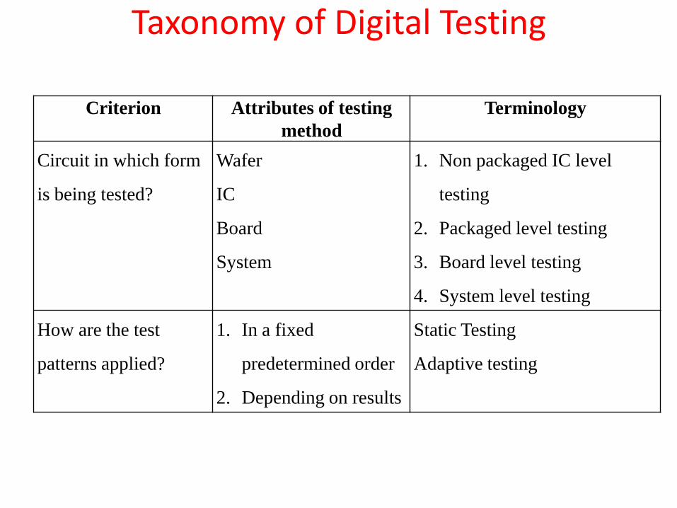
Taxonomy of Digital Testing
Criterion Attributes of testing
method
Terminology
Circuit in which form
is being tested?
Wafer
IC
Board
System
1. Non packaged IC level
testing
2. Packaged level testing
3. Board level testing
4. System level testing
How are the test
patterns applied?
1. In a fixed
predetermined order
2. Depending on results
Static Testing
Adaptive testing

Taxonomy of Digital Testing
Criterion Attributes of testing
method
Terminology
How fast are the test
patterns applied?
1. Much slower than the
normal speed of
operation
2. At normal speed of
operation
1. DC (static) testing
2. At-speed testing
Who verifies the test
results by matching
with golden response?
1. On chip circuit
2. ATE
1. BIST
2. Automatic Test Equipment
(ATE) based testing
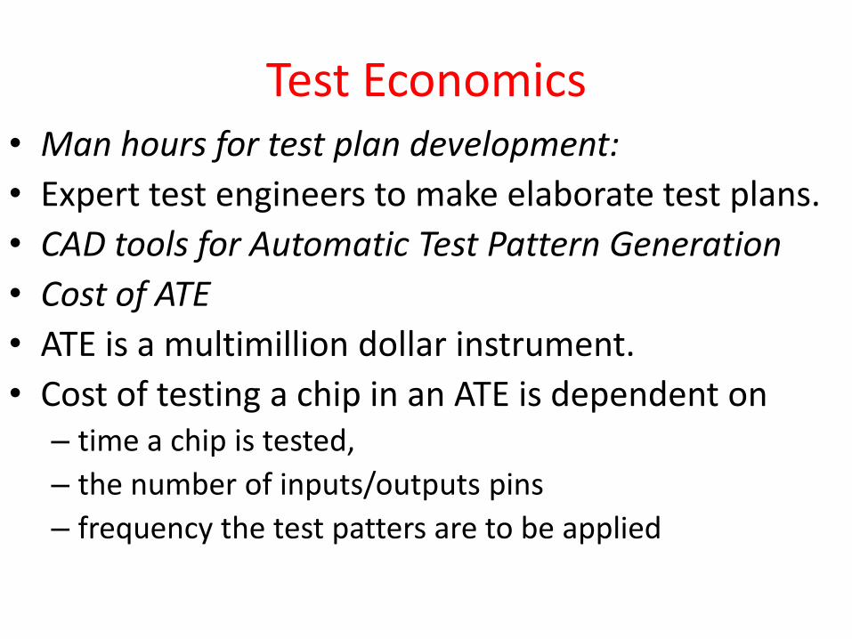
Test Economics • Man hours for test plan development:
• Expert test engineers to make elaborate test plans.
• CAD tools for Automatic Test Pattern Generation
• Cost of ATE
• ATE is a multimillion dollar instrument.
• Cost of testing a chip in an ATE is dependent on – time a chip is tested,
– the number of inputs/outputs pins
– frequency the test patters are to be applied

Test Economics
• DFT/BIST circuitry
– Additional circuitry kept on-chip to help in testing results in raise in chip area
– Rise in area power and lower yield
• At-speed testing by ATE is extremely expensive.
Tradeoff
• Returns
– Proper binning of Chips:
In case of VLSI testing, it is not of much concern as how many chips are binned as faulty, rather important is how many faulty chips are
binned as normal.
So, economic return from “VLSI testing” is the accuracy in shipping functionally perfect chips.

What we will study ?
• Test • Introduction to Digital Testing • Lecture-II: Functional vs. Structural Testing • Lecture-III: Fault Equivalence, Fault Dominance, Fault Collapsing and Checkpoint Theorem • • Fault Simulation and Testability Measures • Lecture-I and II: Circuit Modeling and Algorithms for Fault Simulation
Lecture-III: Combinational SCOAP Measures and Sequential SCOAP Measures
• • Combinational Circuit Test Pattern Generation • Lecture-I: Introduction to Automatic Test Pattern Generation (ATPG) and ATPG Algebras • Lecture-II: Standard ATPG Algorithms

What we will study ?
• Sequential Circuit Testing and Scan Chains
• Lecture-I: ATPG for Single-Clock
Synchronous Circuits
• Lecture-II and III: Scan Chain based
Sequential Circuit Testing
• Built in Self test (BIST)
• Lecture I: Introduction to BIST architecture
• Lecture II and III: Memory BIST

Thank you

Design Verification and Test of Digital VLSI Circuits NPTEL Video Course
Module-VII
Lecture-II
Functional and Structural Testing

Introduction
Test Pattern
No.
Test Pattern Output
1 0000000000000000000000000 0
2 0000000000000000000000001 0
………… …………………………………………….. 0
225 1111111111111111111111111 1
Test patterns for functional testing
Circuit for Bit wise ANDing
Introduction
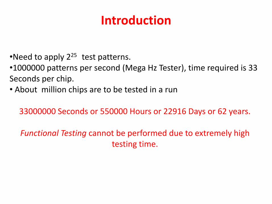
•Need to apply 225 test patterns. •1000000 patterns per second (Mega Hz Tester), time required is 33 Seconds per chip. • About million chips are to be tested in a run
33000000 Seconds or 550000 Hours or 22916 Days or 62 years.
Functional Testing cannot be performed due to extremely high testing time.
Structural Testing
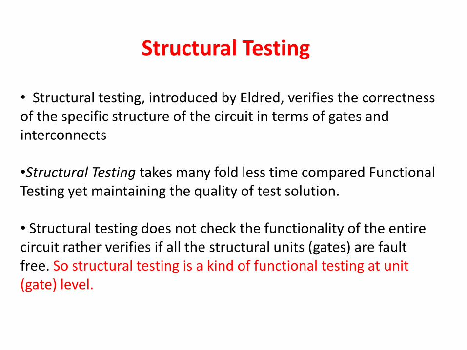
• Structural testing, introduced by Eldred, verifies the correctness of the specific structure of the circuit in terms of gates and interconnects •Structural Testing takes many fold less time compared Functional Testing yet maintaining the quality of test solution. • Structural testing does not check the functionality of the entire circuit rather verifies if all the structural units (gates) are fault free. So structural testing is a kind of functional testing at unit (gate) level.

Structural Testing Example
Test Pattern
(I1,I2,I3,I4,I5)
Output (OG1)
1 00000 0
2 00001 0
… ….. 0
32 11111 1

Structural Testing Example
• Number of test patterns required are 6.25 (=160), which is many fold smaller than those required for functional testing (225).
• Time required for testing the circuit the using a 1 Mega Hz Tester is 0.000016 seconds and for a million samples is 16 seconds.
Structural testing is highly beneficial over functional testing.

Structural Testing—Penalties
• Each individual gate is tested; however, the integration is not tested.
• To test the individual gates, controlling and observing values of intermediary nets in a circuit becomes mandatory, which adds to extra pins and hardware
• Circuit with about a million internal lines needs a million 2-1 Multiplexers and same number of extra pins. This requirement is infeasible.

Structural Testing—Penalties
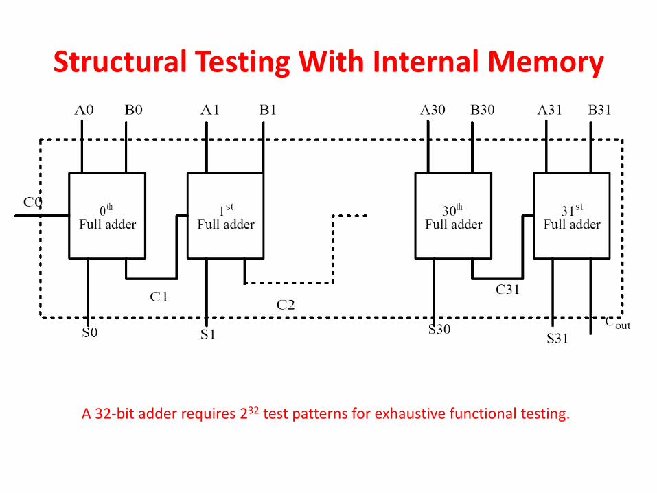
Structural Testing With Internal Memory
A 32-bit adder requires 232 test patterns for exhaustive functional testing.

Structural Testing With Internal Memory
•The 32-bit adder requires 23 test patterns for exhaustive structural testing. •Extra Pins 3 •2 Sets of Registers •2:1 Muxes
Structural Testing With Internal Memory
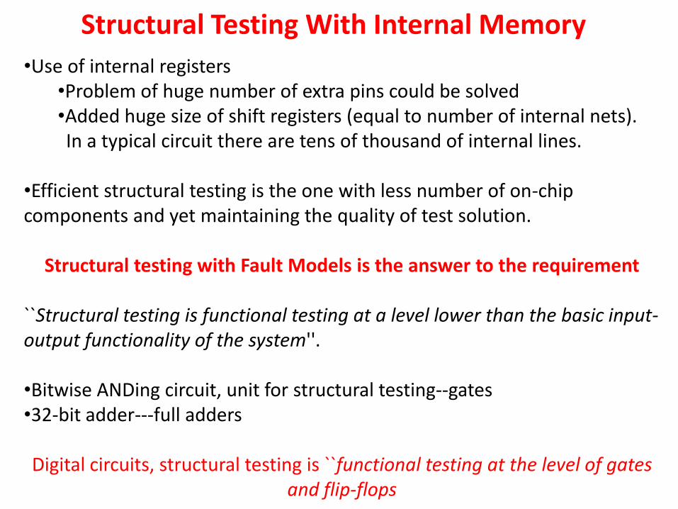
•Use of internal registers •Problem of huge number of extra pins could be solved •Added huge size of shift registers (equal to number of internal nets).
In a typical circuit there are tens of thousand of internal lines. •Efficient structural testing is the one with less number of on-chip components and yet maintaining the quality of test solution.
Structural testing with Fault Models is the answer to the requirement ``Structural testing is functional testing at a level lower than the basic input-output functionality of the system''. •Bitwise ANDing circuit, unit for structural testing--gates •32-bit adder---full adders Digital circuits, structural testing is ``functional testing at the level of gates
and flip-flops

Structural Testing with Fault Models
• Structural testing with fault models involves verifying each unit (gate and flip flop) is free from faults of the fault model.
• A model is an abstract representation of a system. – modeling reduces the complexity in
representation but captures all the properties of the original system required for the application in question.
• Fault model is an abstraction of the real defects in the silicon such that – the faults of the model are easy to represent – should ensure that if one verifies that no faults of
the model are in the circuit, quality of test solution is maintained.

Structural Testing with Fault Models
• Unconnected net I1 is the defect.
• Error is, when I1=1, I2=1,I3=1,I4=1, I5=1 but OG1=0 (should be 1 in normal case).
• Fault is, net I1 is stuck at 0 (when gate is modeled at binary logic level).

Types of Fault Models
• Stuck-at fault model: Faults are fixed (0 or 1) value to a net. Stuck at-0 and Stuck at-1 – single stuck-at fault model
– Multiple stuck at fault model
• Delay fault model: Increase the input to output delay of one logic gate, at a time.
• Bridging Fault: A short between a group of nets – AND Bridge
– OR Bridge

Single Stuck-at Fault Model: Fanouts
•Only one net is faulty at a time. •The faulty net is permanently set to either 0 or 1. •The branches of a fanout net are independent with respect to locations and affect of a stuck-at fault.
If fanout along with all its branches is a single electrical net, then why fault in a branch does not affect the others ?
Single Stuck-at Fault Model
•Several stuck-at faults can be simultaneously present in the circuit.
•A circuit with n lines can have 3n-1 possible stuck line combinations; each net can be: s-a-1, s-a-0, or fault-free.
•Handling multiple stuck-at faults in a typical circuit with some hundreds of thousands of nets is infeasible.
Single stuck-at fault model is manageable in number and also provides acceptable quality of test solution, it is the
most accepted fault model.
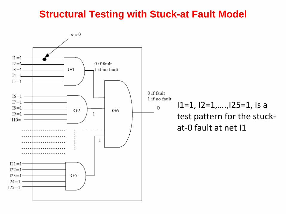
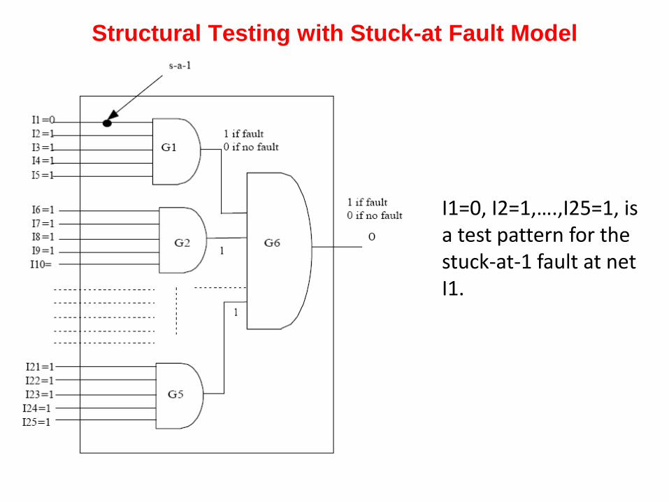
Structural Testing with Stuck-at Fault Model
I1=1, I2=1,….,I25=1, is a test pattern for the stuck-at-0 fault at net I1

Structural Testing with Stuck-at Fault Model
I1=0, I2=1,….,I25=1, is a test pattern for the stuck-at-1 fault at net I1.

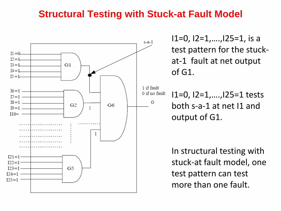
Structural Testing with Stuck-at Fault Model
I1=0, I2=1,….,I25=1, is a test pattern for the stuck-at-1 fault at net output of G1. I1=0, I2=1,….,I25=1 tests both s-a-1 at net I1 and output of G1. In structural testing with stuck-at fault model, one test pattern can test more than one fault.
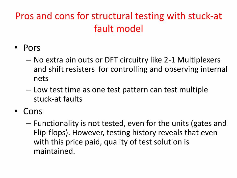
Pros and cons for structural testing with stuck-at fault model
• Pors – No extra pin outs or DFT circuitry like 2-1 Multiplexers
and shift resisters for controlling and observing internal nets
– Low test time as one test pattern can test multiple stuck-at faults
• Cons – Functionality is not tested, even for the units (gates and
Flip-flops). However, testing history reveals that even with this price paid, quality of test solution is maintained.

Comparison of structural and functional testing
Functional testing Structural Testing
Without fault models. With fault models.
Manually generated design
verification test patterns.
Automatic test pattern
generation (ATPG).
Slow and labor intensive. Efficient and automated.
Fault coverage not known Fault Coverage is a quantified
metric.
More Test Patterns Less Test Patterns
Can be applied at the operating
speed.
Difficult to be applied at the
speed the design is expected to
work.
.

Questions and Answers
• What are the problems of structural testing without fault models, if the units are as atomic as gates and as large as arithmetic block like 32-bit adder and 64-multiplier
• How many silicon level defects result in nets getting stuck? Explain relevance of stuck-fault model from that perspective

Thank you

Design Verification and Test of Digital VLSI Circuits NPTEL Video Course
Module-VII
Lecture-III
Fault Equivalence

Introduction
• If there are n nets in a circuit then there can be 2n stuck-at faults
• The number of test patterns is liner in the number of nets in a circuit.
• The total number of test patterns required 2n ??
Structural Testing with Stuck-at Fault Model
I1=0, I2=1,….,I25=1, is a test pattern for the stuck-at-1 fault at net I1.
Structural Testing with Stuck-at Fault Model
I1=0, I2=1,….,I25=1, is a test pattern for the stuck-at-1 fault at net output of G1. I1=0, I2=1,….,I25=1 tests both s-a-1 at net I1 and output of G1. In structural testing with stuck-at fault model, one test pattern can test more than one fault.
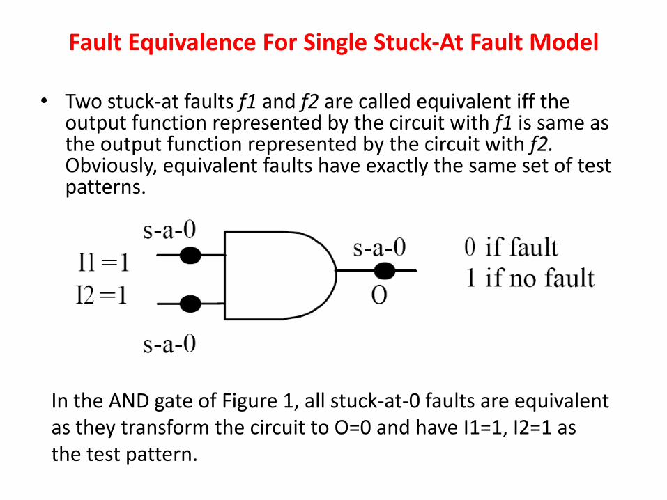
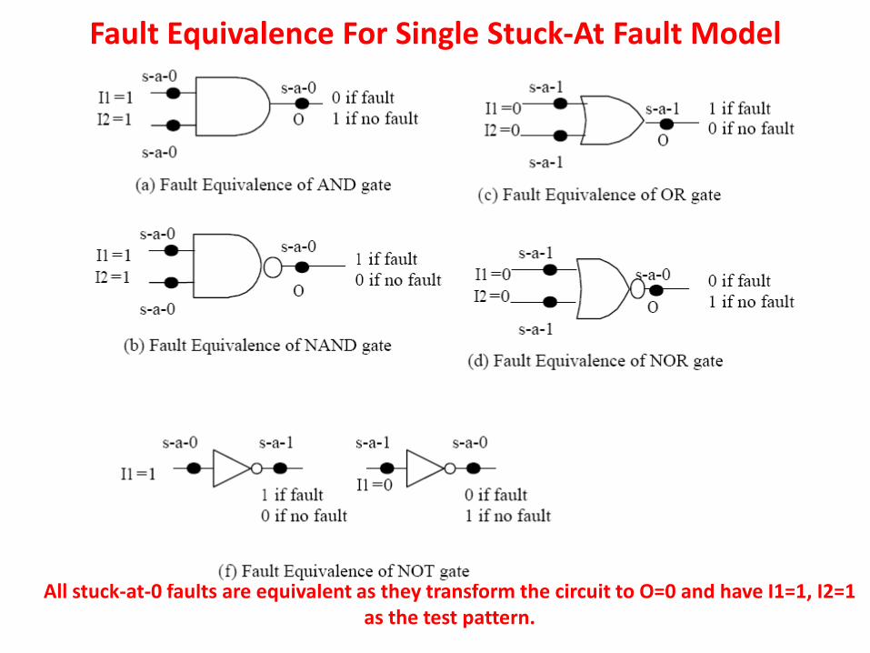
Fault Equivalence For Single Stuck-At Fault Model
• Two stuck-at faults f1 and f2 are called equivalent iff the output function represented by the circuit with f1 is same as the output function represented by the circuit with f2. Obviously, equivalent faults have exactly the same set of test patterns.
In the AND gate of Figure 1, all stuck-at-0 faults are equivalent as they transform the circuit to O=0 and have I1=1, I2=1 as the test pattern.
Fault Equivalence For Single Stuck-At Fault Model
All stuck-at-0 faults are equivalent as they transform the circuit to O=0 and have I1=1, I2=1 as the test pattern.

Fault Equivalence For Single Stuck-At Fault Model: Fanouts
The faults in the stem and branches are not equivalent. Fault at stem results in same output functions of the stem and the branches Fault is in branch I1’, then function of stem is I1=0/1 (as driven) and for the branch I1’ (I1”) function is I1’=0 (I1”=I1). Output function of I1’ is different from I1 and I1”.

Fault Equivalence based Collapsing: Example

Fault Equivalence based Collapsing: Example

Fault Equivalence based Collapsing: Example
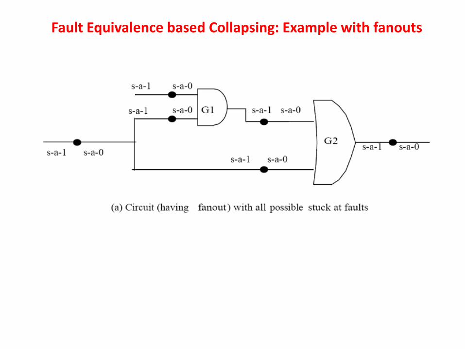
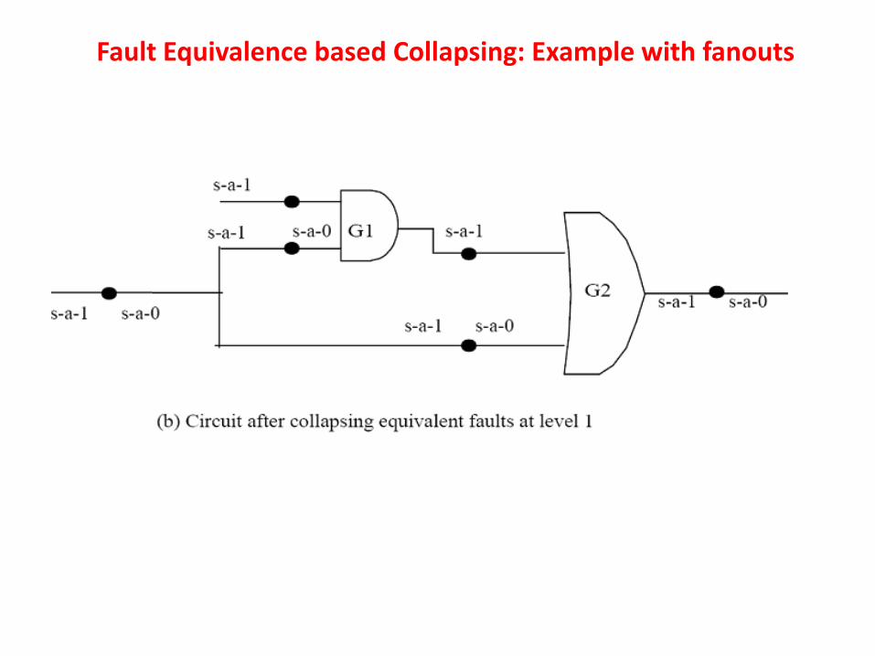
Fault Equivalence based Collapsing: Example with fanouts
Fault Equivalence based Collapsing: Example with fanouts

Fault Equivalence based Collapsing: Example with fanouts

Fault Dominance For Single Stuck-At Fault Model
• If all tests of a stuck-at fault f1 detect fault f2 then f2 dominates f1. If f2 dominants f1 then f2 can be removed and only f1is retained.

Fault Dominance For Single Stuck-At Fault Model

Fault Dominance based Collapsing: Example

Fault Dominance based Collapsing: Example

Fault Dominance based Collapsing: Example

Fault Dominance based Collapsing: Example with fanouts

Fault Dominance based Collapsing: Example with fanouts

Fault Dominance based Collapsing: Example with fanouts

Check point theorem.
– A circuit with no fanouts, s-a-0 and s-a-1 faults is to be
considered only at the primary inputs. So in a fanout free circuit test patters are 2x(Number of primary inputs).
– For circuit with fanout, checkpoints are primary inputs and fanout branches. Faults are to be kept only on the checkpoints .
So a test pattern set that detects all single stuck-at faults of the checkpoints detects all single stuck-at faults in
that circuit.

Questions and Answers
• For what class of circuits, maximum benefit is achieved due to fault collapsing and when the benefits are less? What is the typical number for test patterns required to test these classes of circuits?
• What faults can be collapsed by equivalence in case of XOR gate?
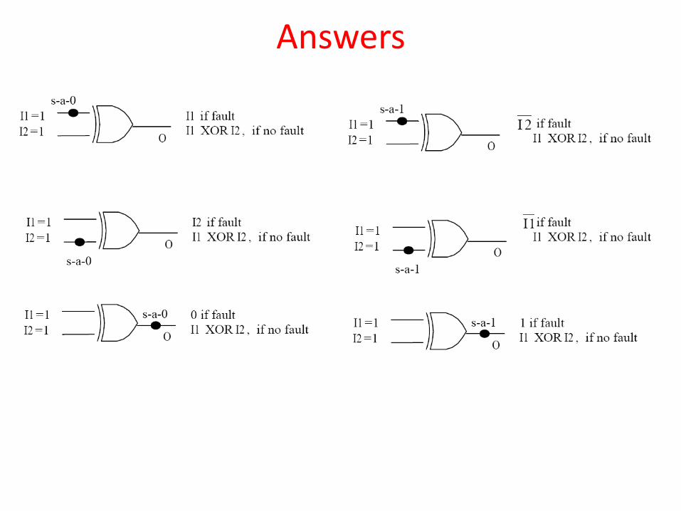
Answers

Thank you