PROCESSING FIR approximations of inverse filters and perfect

Institutionen för systemteknikDepartment of Electrical Engineering
Examensarbete
Design Space Exploration of Time-Multiplexed FIRFilters on FPGAs
Examensarbete utfört i ElektronikSystemvid Tekniska högskolan i Linköping
av
Syed Asad Alam
LiTH-ISY-EX--10/4343--SE
Linköping 2010
Department of Electrical Engineering Linköpings tekniska högskolaLinköpings universitet Linköpings universitetSE-581 83 Linköping, Sweden 581 83 Linköping


Design Space Exploration of Time-Multiplexed FIRFilters on FPGAs
Examensarbete utfört i ElektronikSystem
vid Tekniska högskolan i Linköpingav
Syed Asad Alam
LiTH-ISY-EX--10/4343--SE
Handledare: Oscar Gustafssonisy, Linköping University
Examinator: Oscar Gustafssonisy, Linköping University
Linköping, 10 January, 2010


Avdelning, Institution
Division, Department
Division of Electronics SystemsDepartment of Electrical EngineeringLinköpings universitetSE-581 83 Linköping, Sweden
Datum
Date
2010-01-10
Språk
Language
� Svenska/Swedish
� Engelska/English
�
⊠
Rapporttyp
Report category
� Licentiatavhandling
� Examensarbete
� C-uppsats
� D-uppsats
� Övrig rapport
�
⊠
URL för elektronisk version
http://www.es.isy.liu.se
http://urn.kb.se/resolve?urn=urn:nbn:se:liu:diva-54286
ISBN
—
ISRN
LiTH-ISY-EX--10/4343--SE
Serietitel och serienummer
Title of series, numberingISSN
—
Titel
TitleSvensk titel
Design Space Exploration of Time-Multiplexed FIR Filters on FPGAs
Författare
AuthorSyed Asad Alam
Sammanfattning
Abstract
FIR (Finite-length Impulse Response) filters are the corner stone of many signalprocessing devices. A lot of research has gone into their development as wellas their effective implementation. With recent research focusing a lot on powerconsumption reduction specially with regards to FPGAs, it was found necessaryto explore FIR filters mapping on FPGAs.
Time multiplexed FIR filters are also a good candidate for examination withrespect to power consumption and resource utilization, for example when imple-mented in Field Programmable Gate Arrays (FPGAs). This is motivated by thefact that the usable clock frequency often is higher compared to the required datarate. Current implementations by, e.g., Xilinx FIR Compiler suffer from highpower consumption when the time multiplexing factor is low. Further, it needs tobe investigated how exploiting coefficient symmetry, scaling the coefficients andincreasing the time-multiplexing factor influences the performance.
Nyckelord
Keywords Time-Multiplexed, FIR, FPGA, Xilinx


Abstract
FIR (Finite-length Impulse Response) filters are the corner stone of many signalprocessing devices. A lot of research has gone into their development as wellas their effective implementation. With recent research focusing a lot on powerconsumption reduction specially with regards to FPGAs, it was found necessaryto explore FIR filters mapping on FPGAs.
Time multiplexed FIR filters are also a good candidate for examination withrespect to power consumption and resource utilization, for example when imple-mented in Field Programmable Gate Arrays (FPGAs). This is motivated by thefact that the usable clock frequency often is higher compared to the required datarate. Current implementations by, e.g., Xilinx FIR Compiler suffer from highpower consumption when the time multiplexing factor is low. Further, it needs tobe investigated how exploiting coefficient symmetry, scaling the coefficients andincreasing the time-multiplexing factor influences the performance.
v


Acknowledgments
First of all, I want to thank my supervisor, Associate Professor Oscar Gustafssonfor guidance, inspiration and for giving me the opportunity to conduct my thesis inthe Division of Electronics Systems. I would also like to thank Associate ProfessorKent Palmkvist for helping me out in different aspects of FPGA designing.
Further more, I would like to thank PhD students Muhammad Abbas, FahadQureshi and Zakaullah Sheikh for providing me guidance and helping me out withwriting this Thesis report on LATEX
I would also like to acknowledge M.Sc. student Syed Ahmed Aamir, M.Sc.Muhammad Saad Rahman for being a helpful guide and enabling me to settle inmy life in Linköping.
Also, a big thanks to all the member of the division of Electronics Systems atLinköping University for creating a nice working environment.
Finally, and the most important, from the depths of my heart, my extremegratitude to my mother, who has been such a rock for me during all the turbulenttimes I had initially here and supporting me all the way right upto my Thesiscompletion.
vii

Contents
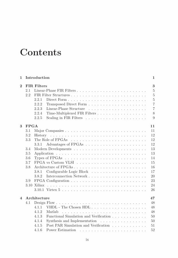
1 Introduction 1
2 FIR Filters 32.1 Linear-Phase FIR Filters . . . . . . . . . . . . . . . . . . . . . . . . 52.2 FIR Filter Structures . . . . . . . . . . . . . . . . . . . . . . . . . . 5
2.2.1 Direct Form . . . . . . . . . . . . . . . . . . . . . . . . . . . 52.2.2 Transposed Direct Form . . . . . . . . . . . . . . . . . . . . 72.2.3 Linear-Phase Structure . . . . . . . . . . . . . . . . . . . . 72.2.4 Time-Multiplexed FIR Filters . . . . . . . . . . . . . . . . . 82.2.5 Scaling in FIR Filters . . . . . . . . . . . . . . . . . . . . . 9
3 FPGA 113.1 Major Companies . . . . . . . . . . . . . . . . . . . . . . . . . . . . 113.2 History . . . . . . . . . . . . . . . . . . . . . . . . . . . . . . . . . 123.3 The Role of FPGAs . . . . . . . . . . . . . . . . . . . . . . . . . . 12
3.3.1 Advantages of FPGAs . . . . . . . . . . . . . . . . . . . . . 123.4 Modern Developments . . . . . . . . . . . . . . . . . . . . . . . . . 133.5 Application . . . . . . . . . . . . . . . . . . . . . . . . . . . . . . . 133.6 Types of FPGAs . . . . . . . . . . . . . . . . . . . . . . . . . . . . 143.7 FPGA vs Custom VLSI . . . . . . . . . . . . . . . . . . . . . . . . 153.8 Architecture of FPGAs . . . . . . . . . . . . . . . . . . . . . . . . . 16
3.8.1 Configurable Logic Block . . . . . . . . . . . . . . . . . . . 173.8.2 Interconnection Network . . . . . . . . . . . . . . . . . . . . 20
3.9 FPGA Configuration . . . . . . . . . . . . . . . . . . . . . . . . . . 233.10 Xilinx . . . . . . . . . . . . . . . . . . . . . . . . . . . . . . . . . . 24
3.10.1 Virtex 5 . . . . . . . . . . . . . . . . . . . . . . . . . . . . . 26
4 Architecture 474.1 Design Flow . . . . . . . . . . . . . . . . . . . . . . . . . . . . . . . 48
4.1.1 VHDL - The Chosen HDL . . . . . . . . . . . . . . . . . . . 484.1.2 Matlab . . . . . . . . . . . . . . . . . . . . . . . . . . . . . 484.1.3 Functional Simulation and Verification . . . . . . . . . . . . 504.1.4 Synthesis and Implementation . . . . . . . . . . . . . . . . 504.1.5 Post PAR Simulation and Verification . . . . . . . . . . . . 514.1.6 Power Estimation . . . . . . . . . . . . . . . . . . . . . . . 52
ix

x Contents
4.2 Architecture - 1 : Fully Parallel Symmetric FIR Filter . . . . . . . 524.2.1 Basic Idea . . . . . . . . . . . . . . . . . . . . . . . . . . . . 524.2.2 Matlab Flow . . . . . . . . . . . . . . . . . . . . . . . . . . 534.2.3 FIR Top . . . . . . . . . . . . . . . . . . . . . . . . . . . . . 554.2.4 Main Controller . . . . . . . . . . . . . . . . . . . . . . . . 574.2.5 Data Memory . . . . . . . . . . . . . . . . . . . . . . . . . . 614.2.6 Coefficient Memory . . . . . . . . . . . . . . . . . . . . . . 624.2.7 Main Filter . . . . . . . . . . . . . . . . . . . . . . . . . . . 634.2.8 Pre-Adder . . . . . . . . . . . . . . . . . . . . . . . . . . . . 664.2.9 Multiply-Accumulate (MAC) . . . . . . . . . . . . . . . . . 664.2.10 Adder Tree . . . . . . . . . . . . . . . . . . . . . . . . . . . 674.2.11 Functional Simulation . . . . . . . . . . . . . . . . . . . . . 684.2.12 Synthesis and Implementation . . . . . . . . . . . . . . . . 694.2.13 Post PAR Simulation . . . . . . . . . . . . . . . . . . . . . 694.2.14 Power Estimation . . . . . . . . . . . . . . . . . . . . . . . 704.2.15 Xilinx FIR Compiler . . . . . . . . . . . . . . . . . . . . . . 70
4.3 Architecture - 2 : Semi Parallel Non-Symmetric FIR Filter . . . . 714.3.1 Basic Idea . . . . . . . . . . . . . . . . . . . . . . . . . . . . 714.3.2 Matlab Flow . . . . . . . . . . . . . . . . . . . . . . . . . . 734.3.3 FIR Top . . . . . . . . . . . . . . . . . . . . . . . . . . . . . 734.3.4 Main Controller . . . . . . . . . . . . . . . . . . . . . . . . 734.3.5 Data Memory . . . . . . . . . . . . . . . . . . . . . . . . . . 774.3.6 Coefficient Memory . . . . . . . . . . . . . . . . . . . . . . 774.3.7 Main Filter . . . . . . . . . . . . . . . . . . . . . . . . . . . 794.3.8 Multiply-Add . . . . . . . . . . . . . . . . . . . . . . . . . . 804.3.9 Accumulator (ACC) . . . . . . . . . . . . . . . . . . . . . . 814.3.10 Functional Simulation . . . . . . . . . . . . . . . . . . . . . 814.3.11 Synthesis and Implementation . . . . . . . . . . . . . . . . 824.3.12 Post PAR Simulation . . . . . . . . . . . . . . . . . . . . . 824.3.13 Power Estimation . . . . . . . . . . . . . . . . . . . . . . . 824.3.14 Xilinx FIR Compiler . . . . . . . . . . . . . . . . . . . . . . 82
5 Results 835.1 Xilinx Resource Facts . . . . . . . . . . . . . . . . . . . . . . . . . 855.2 Altera Resource Facts . . . . . . . . . . . . . . . . . . . . . . . . . 865.3 Comparison-1, Non-Scaled Filter, Parallel vs Semi-Parallel: Slice
Count . . . . . . . . . . . . . . . . . . . . . . . . . . . . . . . . . . 865.4 Comparison-2, Non-Scaled, Parallel vs Semi-Parallel: BRAM Count 865.5 Comparison-3, Non-Scaled, Parallel vs Semi-Parallel: DSP48E Slice
Count . . . . . . . . . . . . . . . . . . . . . . . . . . . . . . . . . . 875.6 Comparison-4, Non-Scaled, Parallel vs Semi-Parallel: Clock Fre-
quency . . . . . . . . . . . . . . . . . . . . . . . . . . . . . . . . . . 885.7 Comparison-5, Non-Scaled, Parallel vs Semi-Parallel: Power Dissi-
pation . . . . . . . . . . . . . . . . . . . . . . . . . . . . . . . . . . 885.8 Comparison-6, Scaled, Parallel vs Semi-Parallel . . . . . . . . . . . 925.9 Comparison-7, Effect of Scaling . . . . . . . . . . . . . . . . . . . . 92
Contents xi
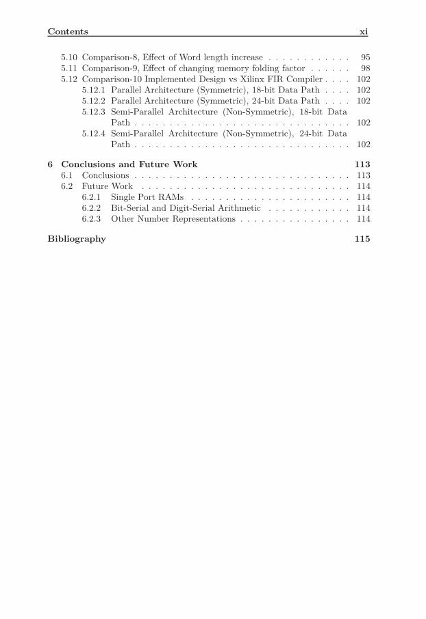
5.10 Comparison-8, Effect of Word length increase . . . . . . . . . . . . 955.11 Comparison-9, Effect of changing memory folding factor . . . . . . 985.12 Comparison-10 Implemented Design vs Xilinx FIR Compiler . . . . 102
5.12.1 Parallel Architecture (Symmetric), 18-bit Data Path . . . . 1025.12.2 Parallel Architecture (Symmetric), 24-bit Data Path . . . . 1025.12.3 Semi-Parallel Architecture (Non-Symmetric), 18-bit Data
Path . . . . . . . . . . . . . . . . . . . . . . . . . . . . . . . 1025.12.4 Semi-Parallel Architecture (Non-Symmetric), 24-bit Data
Path . . . . . . . . . . . . . . . . . . . . . . . . . . . . . . . 102
6 Conclusions and Future Work 1136.1 Conclusions . . . . . . . . . . . . . . . . . . . . . . . . . . . . . . . 1136.2 Future Work . . . . . . . . . . . . . . . . . . . . . . . . . . . . . . 114
6.2.1 Single Port RAMs . . . . . . . . . . . . . . . . . . . . . . . 1146.2.2 Bit-Serial and Digit-Serial Arithmetic . . . . . . . . . . . . 1146.2.3 Other Number Representations . . . . . . . . . . . . . . . . 114
Bibliography 115
xii Contents
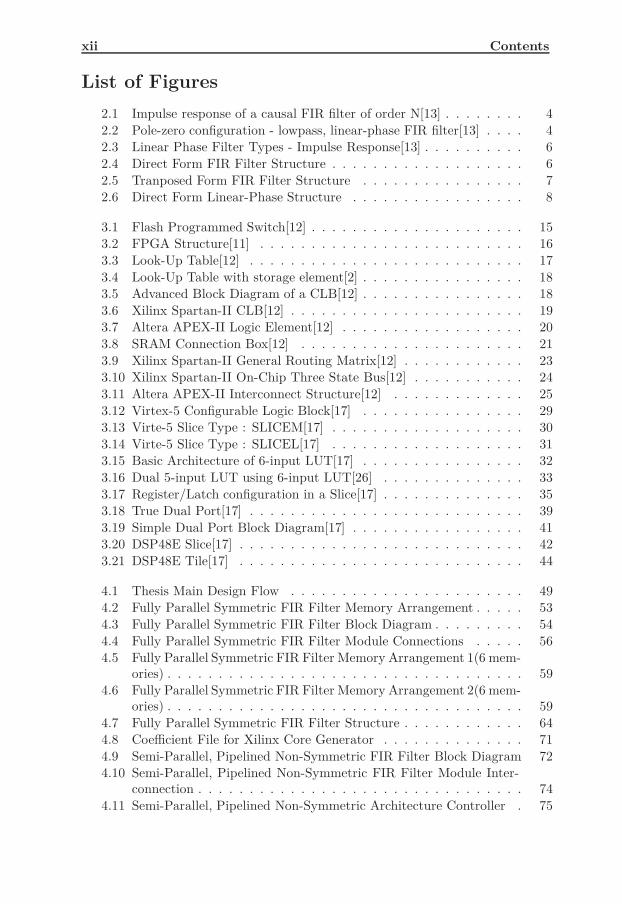
List of Figures
2.1 Impulse response of a causal FIR filter of order N[13] . . . . . . . . 4
2.2 Pole-zero configuration - lowpass, linear-phase FIR filter[13] . . . . 4
2.3 Linear Phase Filter Types - Impulse Response[13] . . . . . . . . . . 6
2.4 Direct Form FIR Filter Structure . . . . . . . . . . . . . . . . . . . 6
2.5 Tranposed Form FIR Filter Structure . . . . . . . . . . . . . . . . 7
2.6 Direct Form Linear-Phase Structure . . . . . . . . . . . . . . . . . 8
3.1 Flash Programmed Switch[12] . . . . . . . . . . . . . . . . . . . . . 15
3.2 FPGA Structure[11] . . . . . . . . . . . . . . . . . . . . . . . . . . 16
3.3 Look-Up Table[12] . . . . . . . . . . . . . . . . . . . . . . . . . . . 17
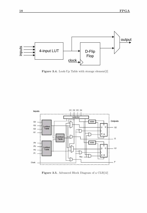
3.4 Look-Up Table with storage element[2] . . . . . . . . . . . . . . . . 18
3.5 Advanced Block Diagram of a CLB[12] . . . . . . . . . . . . . . . . 18
3.6 Xilinx Spartan-II CLB[12] . . . . . . . . . . . . . . . . . . . . . . . 19
3.7 Altera APEX-II Logic Element[12] . . . . . . . . . . . . . . . . . . 20
3.8 SRAM Connection Box[12] . . . . . . . . . . . . . . . . . . . . . . 21
3.9 Xilinx Spartan-II General Routing Matrix[12] . . . . . . . . . . . . 23
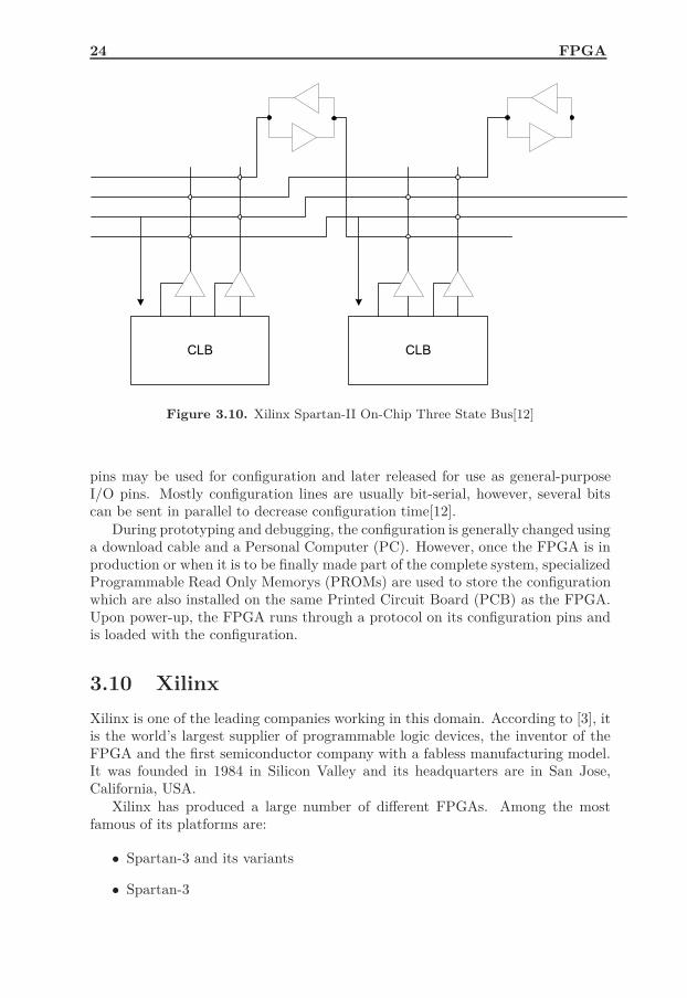
3.10 Xilinx Spartan-II On-Chip Three State Bus[12] . . . . . . . . . . . 24
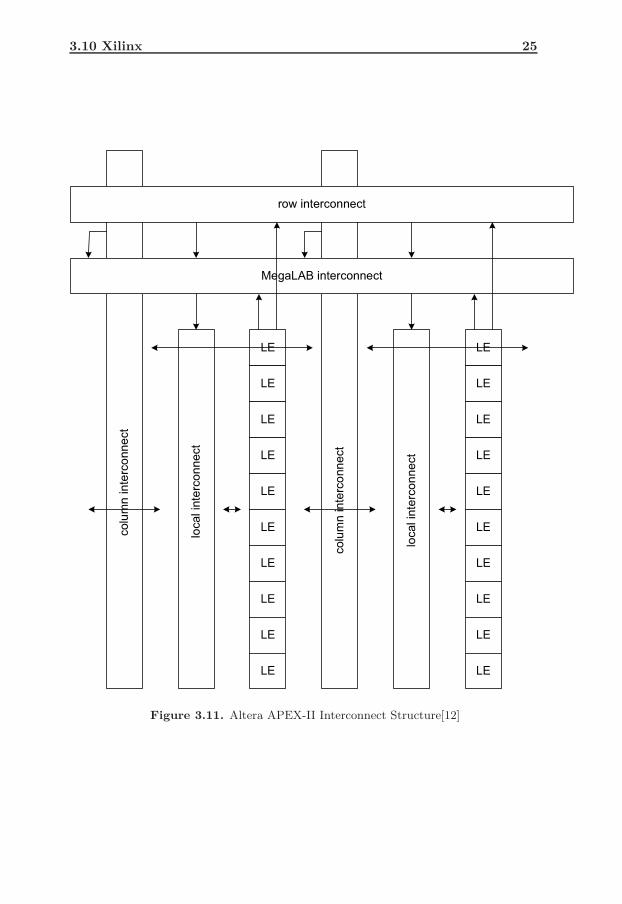
3.11 Altera APEX-II Interconnect Structure[12] . . . . . . . . . . . . . 25
3.12 Virtex-5 Configurable Logic Block[17] . . . . . . . . . . . . . . . . 29
3.13 Virte-5 Slice Type : SLICEM[17] . . . . . . . . . . . . . . . . . . . 30
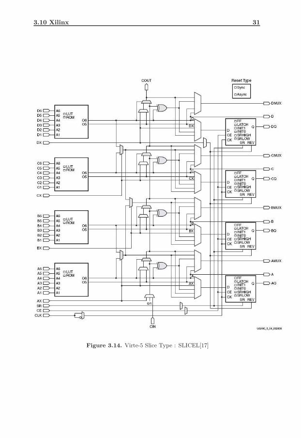
3.14 Virte-5 Slice Type : SLICEL[17] . . . . . . . . . . . . . . . . . . . 31
3.15 Basic Architecture of 6-input LUT[17] . . . . . . . . . . . . . . . . 32
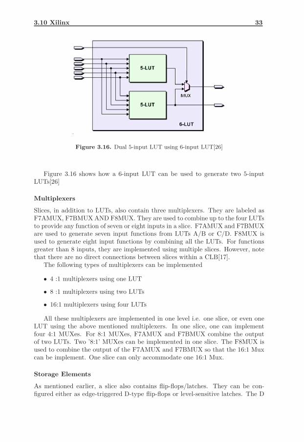
3.16 Dual 5-input LUT using 6-input LUT[26] . . . . . . . . . . . . . . 33
3.17 Register/Latch configuration in a Slice[17] . . . . . . . . . . . . . . 35
3.18 True Dual Port[17] . . . . . . . . . . . . . . . . . . . . . . . . . . . 39
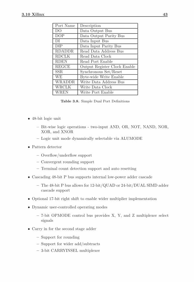
3.19 Simple Dual Port Block Diagram[17] . . . . . . . . . . . . . . . . . 41
3.20 DSP48E Slice[17] . . . . . . . . . . . . . . . . . . . . . . . . . . . . 42
3.21 DSP48E Tile[17] . . . . . . . . . . . . . . . . . . . . . . . . . . . . 44
4.1 Thesis Main Design Flow . . . . . . . . . . . . . . . . . . . . . . . 49
4.2 Fully Parallel Symmetric FIR Filter Memory Arrangement . . . . . 53
4.3 Fully Parallel Symmetric FIR Filter Block Diagram . . . . . . . . . 54
4.4 Fully Parallel Symmetric FIR Filter Module Connections . . . . . 56
4.5 Fully Parallel Symmetric FIR Filter Memory Arrangement 1(6 mem-ories) . . . . . . . . . . . . . . . . . . . . . . . . . . . . . . . . . . . 59
4.6 Fully Parallel Symmetric FIR Filter Memory Arrangement 2(6 mem-ories) . . . . . . . . . . . . . . . . . . . . . . . . . . . . . . . . . . . 59
4.7 Fully Parallel Symmetric FIR Filter Structure . . . . . . . . . . . . 64
4.8 Coefficient File for Xilinx Core Generator . . . . . . . . . . . . . . 71
4.9 Semi-Parallel, Pipelined Non-Symmetric FIR Filter Block Diagram 72
4.10 Semi-Parallel, Pipelined Non-Symmetric FIR Filter Module Inter-connection . . . . . . . . . . . . . . . . . . . . . . . . . . . . . . . . 74
4.11 Semi-Parallel, Pipelined Non-Symmetric Architecture Controller . 75
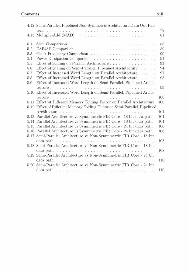
Contents xiii
4.12 Semi-Parallel, Pipelined Non-Symmetric Architecture Data Out Pat-tern . . . . . . . . . . . . . . . . . . . . . . . . . . . . . . . . . . . 78
4.13 Multiply-Add (MAD) . . . . . . . . . . . . . . . . . . . . . . . . . 81
5.1 Slice Comparison . . . . . . . . . . . . . . . . . . . . . . . . . . . . 885.2 DSP48E Comparison . . . . . . . . . . . . . . . . . . . . . . . . . . 895.3 Clock Frequency Comparison . . . . . . . . . . . . . . . . . . . . . 905.4 Power Dissipation Comparison . . . . . . . . . . . . . . . . . . . . 915.5 Effect of Scaling on Parallel Architecture . . . . . . . . . . . . . . . 935.6 Effect of Scaling on Semi-Parallel, Pipelined Architecture . . . . . 945.7 Effect of Increased Word Length on Parallel Architecture . . . . . 975.8 Effect of Increased Word Length on Parallel Architecture . . . . . 985.9 Effect of Increased Word Length on Semi-Parallel, Pipelined Archi-
tecture . . . . . . . . . . . . . . . . . . . . . . . . . . . . . . . . . . 995.10 Effect of Increased Word Length on Semi-Parallel, Pipelined Archi-
tecture . . . . . . . . . . . . . . . . . . . . . . . . . . . . . . . . . . 1005.11 Effect of Different Memory Folding Factor on Parallel Architecture 1005.12 Effect of Different Memory Folding Factor on Semi-Parallel, Pipelined
Architecture . . . . . . . . . . . . . . . . . . . . . . . . . . . . . . . 1015.13 Parallel Architecture vs Symmmetric FIR Core - 18 bit data path 1045.14 Parallel Architecture vs Symmmetric FIR Core - 18 bit data path 1045.15 Parallel Architecture vs Symmmetric FIR Core - 24 bit data path 1065.16 Parallel Architecture vs Symmmetric FIR Core - 24 bit data path 1065.17 Semi-Parallel Architecture vs Non-Symmmetric FIR Core - 18 bit
data path . . . . . . . . . . . . . . . . . . . . . . . . . . . . . . . . 1085.18 Semi-Parallel Architecture vs Non-Symmmetric FIR Core - 18 bit
data path . . . . . . . . . . . . . . . . . . . . . . . . . . . . . . . . 1085.19 Semi-Parallel Architecture vs Non-Symmmetric FIR Core - 24 bit
data path . . . . . . . . . . . . . . . . . . . . . . . . . . . . . . . . 1105.20 Semi-Parallel Architecture vs Non-Symmmetric FIR Core - 24 bit
data path . . . . . . . . . . . . . . . . . . . . . . . . . . . . . . . . 110

xiv Contents
List of Tables
3.1 Virtex-5 LX20T and LX50T Features . . . . . . . . . . . . . . . . 283.2 Virtex-5 LX20T and LX50T Features . . . . . . . . . . . . . . . . 283.3 Logic Resources in One CLB . . . . . . . . . . . . . . . . . . . . . 293.4 Logic Resources in Selected FPGAs . . . . . . . . . . . . . . . . . . 323.5 Type of Distributed RAMs . . . . . . . . . . . . . . . . . . . . . . 363.6 Types of Distributed ROMs . . . . . . . . . . . . . . . . . . . . . . 373.7 True Dual Port Definitions . . . . . . . . . . . . . . . . . . . . . . 403.8 Simple Dual Port Definitions . . . . . . . . . . . . . . . . . . . . . 43
5.1 Slice Comparison . . . . . . . . . . . . . . . . . . . . . . . . . . . . 875.2 DSP48E Comparison . . . . . . . . . . . . . . . . . . . . . . . . . . 895.3 Clock Frequency Comparison, Frequency in MHz . . . . . . . . . . 905.4 Power Dissipation Comparison, Power in mW . . . . . . . . . . . . 915.5 Effect of Scaling-Parallel Architecture . . . . . . . . . . . . . . . . 925.6 Effect of Scaling-Pipelined Architecture . . . . . . . . . . . . . . . 935.7 Effect of Increased Word Length-Parallel Architecture . . . . . . . 955.8 Effect of Increased Word Length-Parallel Architecture . . . . . . . 965.9 Effect of Increased Word Length-Pipelined Architecture . . . . . . 965.10 Effect of Increased Word Length-Pipelined Architecture . . . . . . 975.11 Effect of Different Memory Folding Factor - Parallel Architecture . 985.12 Effect of Different Memory Folding Factor - Pipelined Architecture 995.13 Parallel Architecture vs Symmmetric FIR Core - 18 bit data path 1035.14 Parallel Architecture vs Symmmetric FIR Core - 18 bit data path 1035.15 Parallel Architecture vs Symmmetric FIR Core - 24 bit data path 1055.16 Parallel Architecture vs Symmmetric FIR Core - 24 bit data path 1055.17 Semi-Parallel Architecture vs Non-Symmmetric FIR Core - 18 bit
data path . . . . . . . . . . . . . . . . . . . . . . . . . . . . . . . . 1075.18 Semi-Parallel Architecture vs Non-Symmmetric FIR Core - 18 bit
data path . . . . . . . . . . . . . . . . . . . . . . . . . . . . . . . . 1075.19 Semi-Parallel Architecture vs Non-Symmmetric FIR Core - 24 bit
data path . . . . . . . . . . . . . . . . . . . . . . . . . . . . . . . . 1095.20 Semi-Parallel Architecture vs Non-Symmmetric FIR Core - 24 bit
data path . . . . . . . . . . . . . . . . . . . . . . . . . . . . . . . . 109

AbbreviationsFPGA Field Programmable Gate Array
ASIC Application Specific Integrated Circuit
FIR Finite-length Impulse Response
MAC Multiply-Accumulate
DSP Digital Signal Processing
RAM Random Access Memory
VHDL VHSIC Hardware Description Language
VHSIC Very High Speed Integrated Circuit
ISE Integrated System Environment
IIR Infinite Impulse Response
PROM Programmable Read Only Memory
PLD Programmable Logic Device
CPU Central Processing Unit
CPLD Complex Programmable Logic Device
SERDES Serializer/De-Serializer
LUT Look-Up Table
HDL Hardware Description Language
CLB Configurable Logic Block
IC Integrated Circuit
LE Logic Element
SRAM Static Random Access Memory
CMOS Complementary Metal Oxide Semiconductor
LAB Logic Array Block
GRM General Routing Matrix
PC Personal Computer
PCB Printed Circuit Board
DCM Digital Clock Manager

Contents xvii
PLL Phase-Locked Loop
GMACS Giga Multiply-ACcumulate operations Per Second
GFLOPS Giga Floating Point Operations Per Second
DMIPS Dhrystone Million Instructions Per Second
PCI Peripheral Component Interconnect
CMT Clock Management Tile
ROM Read Only Memory
FIFO First In First Out
ASMBL Application Specific Modular Block
SIMD Single Instruction Multiple Data
RTL Register Transfer Level
PAR Place And Route
MAP Mapping
DUT Design Under Test
XST Xilinx Synthesis Technology
NGD Native Generic Database
DRC Design Rule Check
NCD Native Circuit Description
PCF Physical Constrant File
VCD Value Change Dump
MAD Multiply-Add
SC Slice Count
BC BRAM Count
BRAM Block Random Access Memory
DSPC DSP48E Slice Count
CF Clock Frequency
PD Power Dissipation
NRE Non-Recurring Engineering

Chapter 1
Introduction
Finite-length Impulse Response (FIR) filters are one of the most important compo-nents in many digital signal processing systems. They provide a lot of advantagesover IIR Filters such as linear phase, stability and no feedback.
Traditionally, filter design has been focused on Application Specific IntegratedCircuits (ASICs) using standard cells. But lately, with the fast development ofField Programmable Gate Arrays (FPGAs) with specially built in components forsignal processing, they are fast becoming the hardware of choice.
The operation of FIR filters is based on convolution. Such operations heavilyinvolve Multiply-Accumulate (MAC) Operations. Nearly all FPGAs have specialbuilt in Digital Signal Processing (DSP) Blocks which support fast MAC as well asmultiply operations. This makes FPGA an obvious choice to implement multiplyand MAC intensive FIR filters.
The title of this thesis work in Design Space Exploration of Time-Multiplexed
FIR Filters on FPGAs. There are four components to this title. The first one,Design Space Exploration deals with exploring different ways of implementing FIRfilters on FPGAs with the constraint that one has several cycles to computer onoutput sample, but not enough cycles to just use one multiplier. Not having enoughcycles is the second component, time-multiplexing. FIR and FPGA are the thirdand fourth components. To implement this, two architectures have been imple-mented for Time Multiplexed FIR Filters. Both architectures use Block RAMs andDSP48E Blocks available in Xilinx FPGAs. Special attention has been given toreducing the transition activity of the Block Random Access Memory (RAM)s toreduce the total power consumption. Also, simple scaling has been employed andits effects studied on FPGA resource usage, frequency and power consumption. Inaddition to this, effect of data path word-length and different time-multiplexingfactors have been studied. Finally a comparison has been made between the per-formance of implemented design and FIR core provided by Xilinx.
This document is organized in the following chapters
• Chapter 1 : Introduction
• Chapter 2 : FIR - A brief overview of FIR filters, their properties and
1
2 Introduction
different structures
• Chapter 3 : FPGA - Introduction to FPGA, some examples and detailsabout targeted FPGAs of Xilinx
• Chapter 4 : Architecture - Details about the implemented architectures
• Chapter 5 : Results - Different comparisons and their plots
• Chapter 6 : Conclusions and Future Work - Different conclusions drawn onbasis of results and future direction of this research
The whole design is based on Matlab. Target has been on generation of VHSICHardware Description Language (VHDL) code for different combinations of filterorders and time-multiplexing factors. Time-multiplexing factor has often beenreferred to by the name memory-folding factor. No fixed VHDL code is written.The user controls the filter order, time-multiplexing factor among some otheroptions.
For synthesis, implementation and power estimation, the Integrated SystemEnvironment (ISE) tool provided by Xilinx has been used. Mentor Graphics’ModelSim has been used for functional as well as gate level simulation.
Chapter 2
FIR Filters
FIR are the kind of digital filters whose impulse response to a kronecker deltainput is finite i.e. it settles to zero in a finite number of sample intervals. This isthe reason they are called Finite Impulse Response Filters. This is in contrast toInfinite Impulse Response (IIR). The impulse response of an Nth-order FIR filterlasts for N + 1 samples, and then dies to zero.
The difference equation that defines the output of an FIR filter in terms of itsinput is:
y(n) =
N∑
i=0
h(k)x(n− k) (2.1)
where y is the output, x is the input and h is the coefficient
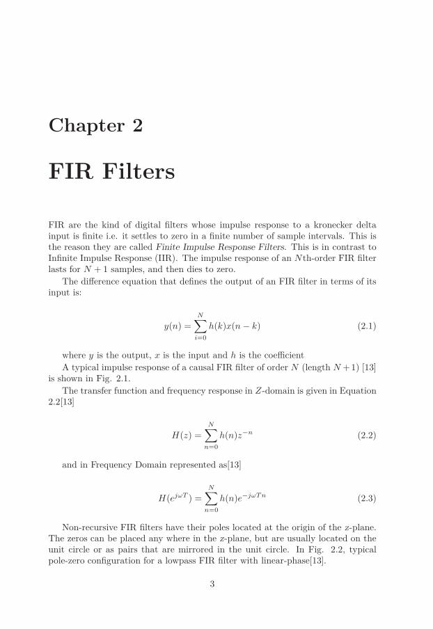
A typical impulse response of a causal FIR filter of order N (length N +1) [13]is shown in Fig. 2.1.
The transfer function and frequency response in Z-domain is given in Equation2.2[13]
H(z) =
N∑
n=0
h(n)z−n (2.2)
and in Frequency Domain represented as[13]
H(ejωT ) =
N∑
n=0
h(n)e−jωTn (2.3)
Non-recursive FIR filters have their poles located at the origin of the z-plane.The zeros can be placed any where in the z-plane, but are usually located on theunit circle or as pairs that are mirrored in the unit circle. In Fig. 2.2, typicalpole-zero configuration for a lowpass FIR filter with linear-phase[13].
3

4 FIR Filters
Figure 2.1. Impulse response of a causal FIR filter of order N[13]
Figure 2.2. Pole-zero configuration - lowpass, linear-phase FIR filter[13]
2.1 Linear-Phase FIR Filters 5
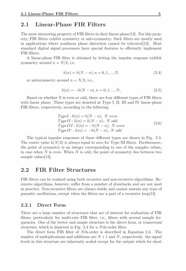
2.1 Linear-Phase FIR Filters
The most interesting property of FIR filters in their linear-phase[13]. For this prop-erty, FIR filters exhibit symmetry or anti-symmetry. Such filters are mostly usedin applications where nonlinear phase distortion cannot be tolerated[13]. Moststandard digital signal processors have special features to efficiently implementFIR filters.
A linear-phase FIR filter is obtained by letting the impulse response exhibitsymmetry around n = N/2, i.e.
h(n) = h(N − n), n = 0, 1, ..., N, (2.4)
or antisymmetry around n = N/2, i.e.,
h(n) = −h(N − n), n = 0, 1, ..., N, (2.5)
Based on whether N is even or odd, there are four different types of FIR filterswith linear phase. These types are denoted as Type I, II, III and IV linear-phaseFIR filters, respectively, according to the following
TypeI : h(n) = h(N − n), N evenTypeII : h(n) = h(N − n), N oddTypeIII : h(n) = −h(N − n), N evenTypeIV : h(n) = −h(N − n), N odd
(2.6)
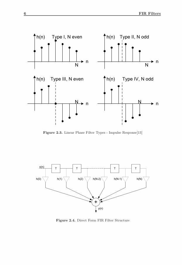
The typical impulse responses of these different types are shown in Fig. 2.3.The centre value h(N/2) is always equal to zero for Type III filters. Furthermore,the point of symmetry is an integer corresponding to one of the samples values,in case when N is even. When N is odd, the point of symmetry lies between twosample values[13].
2.2 FIR Filter Structures
FIR filters can be realized using both recursive and non-recursive algorithms. Re-cursive algorithms, however, suffer from a number of drawbacks and are not usedin practice. Non-recursive filters are always stable and cannot sustain any type ofparasitic oscillations, except when the filters are a part of a recursive loop[13].
2.2.1 Direct Form
There are a large number of structures that are of interest for realization of FIRfilters, particularly for multi-rate FIR filter, i.e., filters with several sample fre-quencies. One of the better and simple structure is the direct form, or transversalstructure, which is depicted in Fig. 2.4 for a Nth-order filter.
The direct form FIR filter of Nth-order is described in Equation 2.3. Thenumber of multiplications and additions are N + 1 and N , respectively. the signallevels in this structure are inherently scaled except for the output which for short
6 FIR Filters
Figure 2.3. Linear Phase Filter Types - Impulse Response[13]
Figure 2.4. Direct Form FIR Filter Structure
2.2 FIR Filter Structures 7
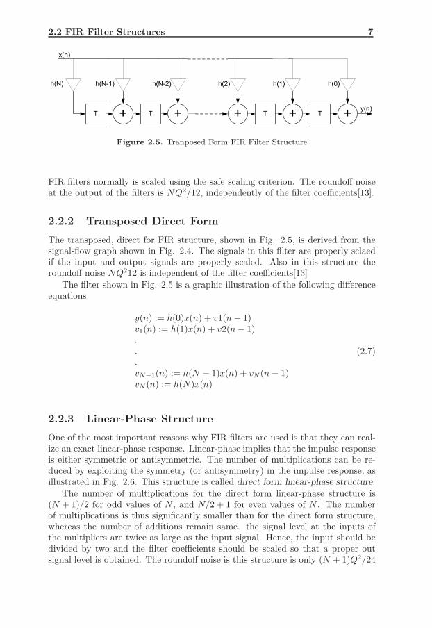
Figure 2.5. Tranposed Form FIR Filter Structure
FIR filters normally is scaled using the safe scaling criterion. The roundoff noiseat the output of the filters is NQ2/12, independently of the filter coefficients[13].
2.2.2 Transposed Direct Form
The transposed, direct for FIR structure, shown in Fig. 2.5, is derived from thesignal-flow graph shown in Fig. 2.4. The signals in this filter are properly sclaedif the input and output signals are properly scaled. Also in this structure theroundoff noise NQ212 is independent of the filter coefficients[13]
The filter shown in Fig. 2.5 is a graphic illustration of the following differenceequations
y(n) := h(0)x(n) + v1(n− 1)v1(n) := h(1)x(n) + v2(n− 1)...vN−1(n) := h(N − 1)x(n) + vN (n− 1)vN (n) := h(N)x(n)
(2.7)
2.2.3 Linear-Phase Structure
One of the most important reasons why FIR filters are used is that they can real-ize an exact linear-phase response. Linear-phase implies that the impulse responseis either symmetric or antisymmetric. The number of multiplications can be re-duced by exploiting the symmetry (or antisymmetry) in the impulse response, asillustrated in Fig. 2.6. This structure is called direct form linear-phase structure.
The number of multiplications for the direct form linear-phase structure is(N + 1)/2 for odd values of N , and N/2 + 1 for even values of N . The numberof multiplications is thus significantly smaller than for the direct form structure,whereas the number of additions remain same. the signal level at the inputs ofthe multipliers are twice as large as the input signal. Hence, the input should bedivided by two and the filter coefficients should be scaled so that a proper outsignal level is obtained. The roundoff noise is this structure is only (N + 1)Q2/24

8 FIR Filters
Figure 2.6. Direct Form Linear-Phase Structure
and (N + 2)Q2/24 for odd values of N and even values of N, respectively. This isindependent of the filter coefficient.
2.2.4 Time-Multiplexed FIR Filters
In this thesis, the focus is on the implementation of Time-Multiplexed FIR Filterson FPGAs. By time-multiplexing, one means that the input data rate is slowerthan the clock rate. Design of such filters is motivated by the fact that the usableclock frequency is generally higher compared to the required data rate. Withtime-multiplexing, it is possible to decrease the number of multipliers at the costof memory cost. But with filter order of around 150-200, the cost of memory ismuch less than the cost of multipliers or MACs(Multiply-Accumulate).
Furthermore, cost of multipliers can be further brought down by utilizing sym-metry. This reduction, tough, comes at a cost of additional adders.
For a given filter orderN , direct form FIR structure needs N+1 multipliers andN adders. The numbers remain same for transposed direct form filters. For linear-phase structures, which utilizes symmetry, the number of multipliers is reduced tohalf i.e. ⌈N/2⌉.
However, when this direct form filters is mapped to a time-multiplexed ar-chitecture, number of multipliers is further reduced. Thus, for a given filter oforder N and time-multiplexing factor ofM , the number of multipliers are reducedto ⌈N/(2M)⌉. However, these multipliers now need to be replaced by Multiply-Accumulate in order to conserve earlier products. Putting it in the form of anequation, we have
2.2 FIR Filter Structures 9
Number of MACs = N / (2M); when N is evenNumber of MACs = (N + 1) / (2M); when N is odd
(2.8)
where N is ’Filter Order’ and M is the ’Time-Multiplexing Factor’Furthermore, if filter is not symmetric/non-symmetric, the number of such
elements now becomes ⌈N/M⌉. Again putting this form into an equation
Number of MACs = N / M ; when N is evenNumber of MACs = (N + 1) / M ; when N is odd
(2.9)
where N and M have the same meaning.Thus, when the input data frequency is much lower, computing resources can
be re-used to reduce the cost and power consumption.
2.2.5 Scaling in FIR Filters
In fixed-point arithmetic, parasitic oscillations can be produced by an overflowof the signal range. These oscillations can even persist after the cause of suchoverflow vanishes. Thus, it is necessary to insure that permanent oscillationsare not sustained within a filter. It is also of utmost importance that frequentoccurrences of signal overflow does not occur as it causes large distortions.
The probability of overflow, however, can be reduced by decreasing the signallevels inside the filter. This can be achieved by the insertion of scaling multipliersinside the filter. Care must be taken to insure that the scaling multiplier does notchange the transfer function of the filter nor does it decrease the signal level somuch that the Signal-to-Noise (SNR) becomes poor.
There are mainly two types of scaling strategies
• Safe Scaling
• Lp-Norms
Safe scaling is generally used for short length FIR filters. Lp-Norms are muchbetter because they utilize the signal range efficiently. However, since due to time-multiplexing, a long filter is reduced to a number of short filters, and thus safescaling is enough for such filters.
Safe Scaling
The scaling policy of safe scaling is that if the input to the filter does not overflow,the input to the multiplier will never overflow. In such a scaling, one takes thesum of absolute values of filter coefficients at the critical node, and divide thecoefficients with this value. Critical node is the node where scaling is needed andis generally the input to the multiplier.

Chapter 3
FPGA
FPGA is an integrated circuit designed to be configured by the customer or de-signer after being manufactured. Thus they are programmable. Its configurationis generally specified using a Hardware Description Language (HDL), which is alsoused for designing ASICs.
In the not-so-distant past, the question used to be, Can you do that task inan FPGA? With the advent of modern FPGA devices, however, the question hasbecome, Why would you not use an FPGA? Modern FPGAs complexity rivals thatof ASICs. The chips contain hundreds of thousands of flip-flops, multi megabitsof RAM, thousands of DSP slices, multiple soft or hard processor cores, multipleSerializer/De-Serializer (SERDES) channels, and more[1].
FPGAs can be used to implement any logic function. Furthermore, this func-tionality can be updated even after selling it to the customer. The ability tore-program without going through the whole fabrication cycle an ASIC must goprovides an enormous advantage, especially for low-volume applications.
The building block of an FPGA is called ’logic block’. Logic blocks are essen-tially Look-Up Table (LUT) which can be configured to complex combinatorialfunctions or simply logic gates. The LUT can be combined together to form alarger block which might contain a multiplexer, flip flop and even a carry chain.
3.1 Major Companies
There are two major companies manufacturing FPGAs. They are
1. Xilinx
2. Altera
Each company has produced a string of ultra-modern, low-cost, highly special-ized FPGAs with a host of facilities for signal processing, advance communicationetc.
11

12 FPGA
3.2 History
The FPGA industry emerged from Programmable Read Only Memory (PROM)and Programmable Logic Devices (PLDs) [2]. They both can be programmed inthe factory or in the field (field programmable), however programmable logic washard-wired between logic gates.
The first company to formally begin manufacturing FPGAs was Xilinx in 1984.Among the initial FPGAs were XC2064, XC4000 and XC6200 which contained lessthan 100 Configurable Logic Blocks (CLBs) and 3-input LUTs. These devices laidthe foundation of a new technology and market.
Xilinx continued unchallenged and quickly growing from 1985 to the mid-1990s,when competitors came up, reducing the market-share significantly. By 1993, 18percent of the market was served by Actel[5]. The 1990s were an explosive periodof time for FPGAs, both in sophistication and the volume of production. In theearly 1990s, FPGAs were primarily used in telecommunications and networking.By the end of the decade, FPGAs found their way into consumer, automotive, andindustrial applications[10].
In the first decade of the new century, extremely complex FPGAs were mar-keted, specially by Xilinx and its main competitor Altera. Platforms like Spartan-III, Virtex-6 by Xilinx and Cyclone-III, Stratix-IV enabled designers to implementextremely complex applications in FPGAs.
3.3 The Role of FPGAs
Field Programmable Gate Arrays (FPGAs) fill a need in the design space of digitalsystems, complementary to the role played by microprocessors. Microprocessorscan be used in a variety of environments, but because they rely on software toimplement functions, they are generally slower and more power hungry than cus-tom chips. Similarly, FPGAs are not custom parts, so they are not as good atany particular function as a dedicated chip designed for that application. FPGAsare generally slower and burn more power than custom logic. FPGAs are alsorelatively expensive although it is often tempting to think that a custom-designedchip would be cheaper[12]
3.3.1 Advantages of FPGAs
FPGAs have their disadvantages as mentioned above, however, they have com-pensating advantages, largely due to the fact that they are standard parts[12].
1. There is no need to wait for the chip to be fabricated to obtain a working chip.The design can be programmed in to the FPGA and tested immediately.
2. FPGAs are excellent prototyping tools. Using the FPGA in the final designmakes the jump from prototype to the final product much smaller and easilynegotiable.
3. The same FPGA can be used in several different designs, reducing costs.

3.4 Modern Developments 13
3.4 Modern Developments
For many years FPGAs were seen primarily as glue logic and prototyping devices.Today, they are used in all sorts of digital circuit design[12]:
1. as part of high-speed telecommunications equipment.
2. as video accelerators in home personal video recorders
A recent trend has been to take the coarse-grained architectural approach astep further by combining the logic blocks and interconnects of traditional FP-GAs with embedded microprocessors and related peripherals to form a complete“system on a programmable chip”[2]. This work mirrors the architecture by RonPerlof and Hana Potash of Burroughs Advanced Systems Group which combined areconfigurable Central Processing Unit (CPU) architecture on a single chip calledthe SB24. That work was done in 1982. Examples of such hybrid technologies canbe found in the Xilinx Virtex-II PRO and Virtex-4 devices, which include one ormore PowerPC processors embedded within the FPGA’s logic fabric. The AtmelFPSLIC is another such device, which uses an AVR processor in combination withAtmel’s programmable logic architecture.
An alternate approach to using hard-macro processors is to make use of “soft”processor cores that are implemented within the FPGA logic.
As previously mentioned, many modern FPGAs have the ability to be repro-grammed at “run time”, and this is leading to the idea of reconfigurable computingor reconfigurable systems -CPUs that reconfigure themselves to suit the task athand. The Mitrion Virtual Processor from Mitrionics is an example of a recon-figurable soft processor, implemented on FPGAs. However, it does not supportdynamic reconfiguration at runtime, but instead adapts itself to a specific program.
Additionally, new, non-FPGA architectures are beginning to emerge. Software-configurable microprocessors such as the Stretch S5000 adopt a hybrid approachby providing an array of processor cores and FPGA-like programmable cores onthe same chip.
3.5 Application
FPGAs have a wide range of applications [2], some are listed below:
1. Signal Processing
2. Software-defined radio
3. Aerospace and Defence
4. ASIC Prototyping
5. Medical Imaging
6. Computer Vision

14 FPGA
7. Telecommunication
8. Speech Recognition
9. Computer Hardware Emulation
Originally, FPGAs were a competitor to Complex Programmable Logic Devices(CPLDs) and mostly were used as glue logic. But as their size, capabilities andspeed increased they started being used in a wide range of increasingly complexand diverse applications. They are now being marketed as complete System-on-Chip solutions.
FPGAs became even more used in signal processing applications by the in-troduction of dedicated multipliers and then multiply-accumulate, which enableddesigners to implement multiplier and Multiply-Accumulate (MAC) intensive ap-plications in FPGAs which were fast in speed and low on area.
The built-in parallelism of resources in FPGA allows massively parallel appli-cations to be easily implemented in an FPGA. It allows for a high throughput evenat low MHz clock rates. This has given birth to a new type of processing calledreconfigurable processing, where FPGAs perform time intensive tasks instead ofsoftware.
Since a single unit cost of an FPGA is generally more than an ApplicationSpecific Integrated Circuit (ASIC) , they normally find applications in low-volumeproducts where the company does not need to incur the high Non-RecurringEngineering (NRE) cost of an ASIC . However, with recent advancements inFPGA Technology has enabled low cost FPGAs which in turn has made FPGAincreasingly viable in high volume products well.
3.6 Types of FPGAs
There are three main types of FPGAs[11].
• Static Random Access Memory (SRAM)
• Anti-Fuse
• Flash
Xilinx and Altera both sold early SRAM-based FPGAs. An alternative ar-chitecture was introduced by Actel, which used an anti-fuse architecture. Thisarchitecture was not re-programmable in the field, which arguably was an advan-tage in situations that did not require re-configuration. The Actel FPGAs used amux-oriented logic structure organized around wiring channels.
SRAM stands for Static Random Access Memory (RAM). It is based on thestatic memory technology. Such a FPGA is volatile i.e. at power up it has to beprogrammed using external boot devices. They hold their configurations in staticmemory, output of which is directly connected to another circuit and its statecontrols the circuit being configured [12]. It has many advantages[12].
• They can be easily programmed, even during system operation
3.7 FPGA vs Custom VLSI 15
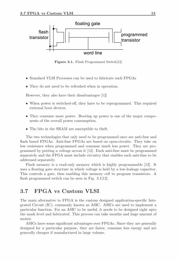
Figure 3.1. Flash Programmed Switch[12]
• Standard VLSI Processes can be used to fabricate such FPGAs
• They do not need to be refreshed when in operation.
However, they also have their disadvantages [12]
• When power is switched-off, they have to be reprogrammed. This requiredexternal boot devices.
• They consume more power. Booting up power is one of the major compo-nents of the overall power consumption.
• The bits in the SRAM are susceptible to theft.
The two technologies that only need to be programmed once are anti-fuse andflash based FPGAs. Anti-fuse FPGAs are based on open-circuits. They take onlow resistance when programmed and consume much less power. They are pro-grammed by putting a voltage across it [12]. Each anti-fuse must be programmedseparately and the FPGA must include circuitry that enables each anti-fuse to beaddressed separately.
Flash memory is a read-only memory which is highly programmable [12]. Ituses a floating gate structure in which voltage is held by a low-leakage capacitor.This controls a gate, thus enabling this memory cell to program transistors. Aflash programmed switch can be seen in Fig. 3.1[12].
3.7 FPGA vs Custom VLSI
The main alternative to FPGA is the custom designed application-specific Inte-grated Circuit (IC), commonly known as ASIC. ASICs are used to implement aparticular function. For an ASIC to be useful, it needs to be designed right uptothe mask level and fabricated. This process can take months and huge amount ofmoney.
ASICs have some significant advantages over FPGAs. Since they are generallydesigned for a particular purpose, they are faster, consume less energy and aregenerally cheaper if manufactured in large volume.

16 FPGA
Figure 3.2. FPGA Structure[11]
However, there are dis-advantages too. They are expensive, require more timeto be fabricated affecting time-to-market. In an increasingly competitive market,this is a critical issue. Furthermore, with recent advancement and tremendousgrowth in FPGAs along with the inherent programmability, they are expected totake a larger share of the IC market for high-density chips.
3.8 Architecture of FPGAs
Generally [12] FPGA has three main types of elements
• Combinational Logic
• Interconnect
• I/O pins
In Fig. 3.2, the basic structure of an FPGA that shows all the elements. Thecombinational logic is normally divided into relatively small units called LogicElements (LEs) or Configurable Logic Blocks (CLBs). With the advancement intechnology, these blocks can now also support sequential circuits. This can beachieved with a built-in flip flop. The interconnections are programmable whichare organized into channels and are used to route signals between CLBs and I/Oblocks. There are different types of interconnects depending on the distance be-tween the CLBs to be connected; clocks are provided with dedicated interconnec-tion networks for fast routing of the clock with minimum skew. Also, there is aclock circuitry for driving the clock signals to each flip-flop in each logic block.

3.8 Architecture of FPGAs 17
Figure 3.3. Look-Up Table[12]
3.8.1 Configurable Logic Block
The CLBs are generally composed of Look-Up Tables (LUTs). They are sometimesreferred to as “Logic Elements” or “LEs”. A block diagram of a basic LUT isshown in Fig. 3.3. In SRAM based FPGAs, a LUT is used to implement a truthtable. Each address in the SRAM represents a combination of inputs to the logicelement. The value stored at that address represents the value of the function forthat input combination. An n-input function requires an SRAM with 2n locations.As a result, the n-input LE can represent 22n functions. A typical logic elementhas four inputs. The delay through the LUT is independent of the bits stored inthe SRAM, so the delay through the logic element is the same for all functions.This means that, for example, a LUT based LE will exhibit the same delay for a 4-input XOR and a 4-input NAND. In contrast, the same XOR function built usingstatic Complementary Metal Oxide Semiconductor (CMOS) Logic is significantlyslower than the NAND function. Although, the static CMOS implementation isgenerally faster than the LE.
LEs generally has registers; flip-flops and latches, as well as combinationallogic. A flip-flop or latch is small compared to the combinational logic element.A LUT with a memory element is shown in Fig. 3.4. Here it is shown that boththe unregistered and registered output is connected to the main output through amultiplexer. More complex logic blocks are also possible. For example, many logicelements also contain special circuitry for addition. Many FPGAs also incorporatespecialized adder logic in the logic element. The critical component of an adderis the carry chain, which can be implemented much more efficiently in specializedlogic than it can using standard lookup table techniques.
A more advanced block diagram of a CLB is shown in Fig. 3.5[11]. In thisfigure, inputs C1 through C4 allow outputs from other CLBs to be input to thisparticular CLB so that CLBs can be cascaded for advanced functions. Few exam-ples from [12] of advance and complex CLBs are given below
18 FPGA
Figure 3.4. Look-Up Table with storage element[2]
Figure 3.5. Advanced Block Diagram of a CLB[12]

3.8 Architecture of FPGAs 19
Figure 3.6. Xilinx Spartan-II CLB[12]
Xilinx Spartan-II
The Spartan-II combinational block [14] consists of two identical slices, with eachslice containing a LUT, some carry logic, and register. One slice is shown in 3.6.
There are two logic cells in one slice. A pair of 4-bit LUTs form the foundationof a logic cell. Each LUT can also be used as a 16-bit synchronous RAM or as a16-bit shift register. It also contains carry logic for each LUT so that additionscan be performed. The multiplexer is used to combine the results of the twofunction generators in a slice. Another multiplexer combines the outputs of themultiplexers in the two slices, generating a result for the entire CLB.
Each CLB also contains two three-state drivers (known as BUFTs) that canbe used to drive on-chip busses.
20 FPGA
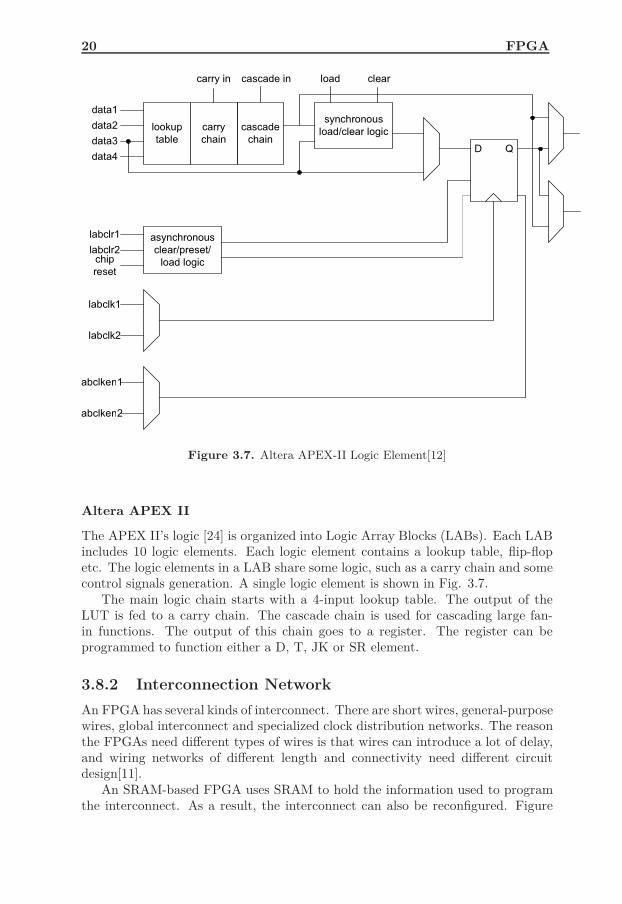
Figure 3.7. Altera APEX-II Logic Element[12]
Altera APEX II
The APEX II’s logic [24] is organized into Logic Array Blocks (LABs). Each LABincludes 10 logic elements. Each logic element contains a lookup table, flip-flopetc. The logic elements in a LAB share some logic, such as a carry chain and somecontrol signals generation. A single logic element is shown in Fig. 3.7.
The main logic chain starts with a 4-input lookup table. The output of theLUT is fed to a carry chain. The cascade chain is used for cascading large fan-in functions. The output of this chain goes to a register. The register can beprogrammed to function either a D, T, JK or SR element.
3.8.2 Interconnection Network
An FPGA has several kinds of interconnect. There are short wires, general-purposewires, global interconnect and specialized clock distribution networks. The reasonthe FPGAs need different types of wires is that wires can introduce a lot of delay,and wiring networks of different length and connectivity need different circuitdesign[11].
An SRAM-based FPGA uses SRAM to hold the information used to programthe interconnect. As a result, the interconnect can also be reconfigured. Figure

3.8 Architecture of FPGAs 21
Figure 3.8. SRAM Connection Box[12]
3.8 shows a simple version of an interconnection point, often known as a connec-tion box. A programmable connection between two wires is make by a CMOStransistor (Pass Transistor). The pass transistor’s gate is controlled by a staticmemory program bit (D Register in this figure). This transistor also conductsbidirectionally, however it is relatively slow, particularly on a signal path thatincludes several interconnection points in a row[12].
Performance
In comparison to custom chips, FPGA wiring with programmable interconnect isslower. There are two reasons
• Pass Transistor
• Wire Lengths
The pass transistor is not a perfect on-switch, so a programmable interconnec-tion point is slower than wires connected by vias. Furthermore, FPGA wires arelonger than would be necessary because they are designed to connect a variety oflogic elements and other FPGA resources. This would introduce extra capacitanceand resistance that slows the signals on the net. On the other hand, in customchips, wires can be made only as long as needed[12].
Types
As indicated earlier, there are different types of interconnects in an FPGA, essen-tially to take advantage of the logic in the LEs. Wiring is often organized intodifferent categories depending on its structure and intended use[12].
• Short Wires: They connect only local Logic Elements. They do not takeup much space and only introduce short delays. Example: Carry Chainsthrough the LEs.
22 FPGA
• Global Wires: Designed for long distance communication. they have fewerconnection points as compared to local connections which reduces theirimpedance.
• Special Wires: Dedicated to either distribute clocks or other register controlsignals.
The next examples are taken from [12] and describe the interconnect systemsin the two FPGAs discussed in 3.8.1.
Xilinx Spartan-II
The Spartan-II includes several types of interconnect. They are listed below
• Local
• General Purpose
• Input/Output
• Global
• Clock
The local interconnect system provides the several kinds of connections. Itconnects the
• Look-Up Tables
• Flip-Flops
• General Purpose Interconnect
It also provides internal CLB feedback. Furthermore, it also includes some di-rect paths for high-speed connections between horizontally adjacent CLBs. Thesepaths can be used for arithmetic, shift registers or other functions that need struc-tured layout and short connections.
The general-purpose routing network provides the bulk of the routing resources.This includes the following types of interconnect:
• A General Routing Matrix (GRM). This is a switch matrix which is usedto connect horizontal and vertical routing channels along with connectionsbetween the CLBs and the routing channels.
• Twenty Four single-length lines to connect each GRM to the ’4’ nearest andadjacent.
• Hex lines route these GRM signals to the GRMs six block away. Theselines provide longer interconnect. The hex lines include buffers to drive thelonger wires. There are a total of 96 hex lines among which one-third arebidirectional and the rest unidirectional.
3.9 FPGA Configuration 23
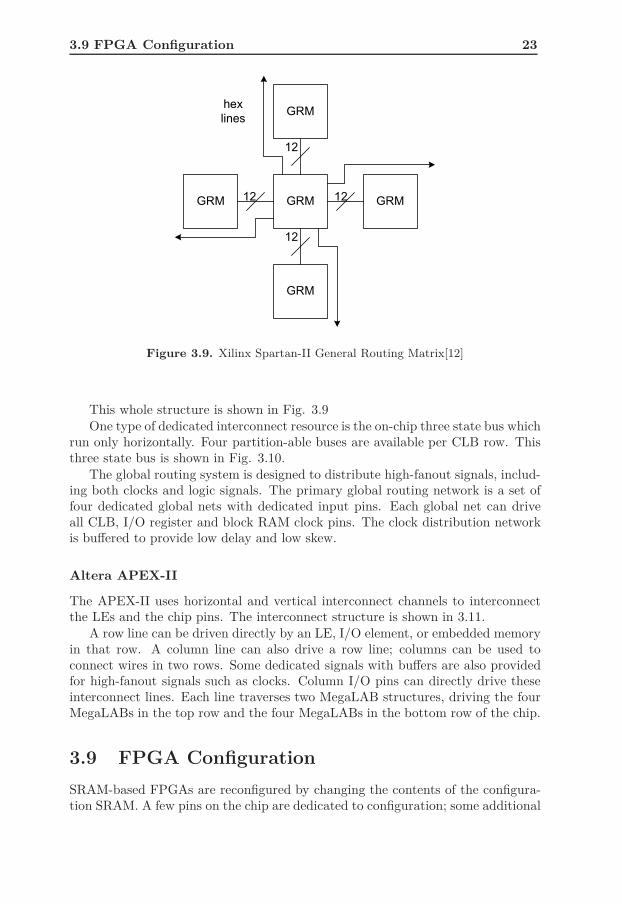
Figure 3.9. Xilinx Spartan-II General Routing Matrix[12]
This whole structure is shown in Fig. 3.9One type of dedicated interconnect resource is the on-chip three state bus which
run only horizontally. Four partition-able buses are available per CLB row. Thisthree state bus is shown in Fig. 3.10.
The global routing system is designed to distribute high-fanout signals, includ-ing both clocks and logic signals. The primary global routing network is a set offour dedicated global nets with dedicated input pins. Each global net can driveall CLB, I/O register and block RAM clock pins. The clock distribution networkis buffered to provide low delay and low skew.
Altera APEX-II
The APEX-II uses horizontal and vertical interconnect channels to interconnectthe LEs and the chip pins. The interconnect structure is shown in 3.11.
A row line can be driven directly by an LE, I/O element, or embedded memoryin that row. A column line can also drive a row line; columns can be used toconnect wires in two rows. Some dedicated signals with buffers are also providedfor high-fanout signals such as clocks. Column I/O pins can directly drive theseinterconnect lines. Each line traverses two MegaLAB structures, driving the fourMegaLABs in the top row and the four MegaLABs in the bottom row of the chip.
3.9 FPGA Configuration
SRAM-based FPGAs are reconfigured by changing the contents of the configura-tion SRAM. A few pins on the chip are dedicated to configuration; some additional
24 FPGA
Figure 3.10. Xilinx Spartan-II On-Chip Three State Bus[12]
pins may be used for configuration and later released for use as general-purposeI/O pins. Mostly configuration lines are usually bit-serial, however, several bitscan be sent in parallel to decrease configuration time[12].
During prototyping and debugging, the configuration is generally changed usinga download cable and a Personal Computer (PC). However, once the FPGA is inproduction or when it is to be finally made part of the complete system, specializedProgrammable Read Only Memorys (PROMs) are used to store the configurationwhich are also installed on the same Printed Circuit Board (PCB) as the FPGA.Upon power-up, the FPGA runs through a protocol on its configuration pins andis loaded with the configuration.
3.10 Xilinx
Xilinx is one of the leading companies working in this domain. According to [3], itis the world’s largest supplier of programmable logic devices, the inventor of theFPGA and the first semiconductor company with a fabless manufacturing model.It was founded in 1984 in Silicon Valley and its headquarters are in San Jose,California, USA.
Xilinx has produced a large number of different FPGAs. Among the mostfamous of its platforms are:
• Spartan-3 and its variants
• Spartan-3
3.10 Xilinx 25
Figure 3.11. Altera APEX-II Interconnect Structure[12]

26 FPGA
• Virtex
• Virtex-II and its variants
• Virtex-4 and its variants
• Virtex-5 and its variants
• Virtex-6
The Spartan series primarily targets those applications which have a low-powerfootprint, extreme cost sensitivity and high-volume, for example, display, set-topboxes, wireless routers and other applications. The latest series in the Spartanfamily is Spartan-6 which has been built on the latest 45-nm technology.
On the other hand, the Virtex family targets complex and specialized appli-cations such as wired and wireless equipment, advanced medical equipment anddefense systems. It also includes embedded fixed function hardware such as mul-tipliers, memories, serial transceivers and microprocessor cores.
The Virtex-II Pro family was the first to include the PowerPC processor. Italso had built-in serial transceivers. The Virtex-4 was introduced in 2004 andmanufactured on a 1.2V, 90-nm, triple-oxide process technology. It consists ofthree families, LX - focused on logic design, FX - focused on embedded processingand connectivity and SX - focused on digital signal processing[3].
The Virtex-5 series was introduced in 2006 and is the focus of this Thesis. Init, Xilinx introduced the 6-input LUTs and was fabricated using a 65-nm, 1.0V,triple-oxide process technology. Virtex-5 also had different families focusing ondifferent types of design. The latest in the Virtex family is the Virtex-6. It is builton 40-nm process for highly computing intensive electronic systems[3].
In this thesis, the focus was the mapping of time-multiplexed FIR filters onFPGAs and special focus was on the utilization of DSP and Block RAM resources.A maximum FIR filter order 128 was generated. The LXT-family has enough DSPand Block RAM resources to support all the test filters. Thus, the Virtex-5 LXfamily was chosen for design implementation.
3.10.1 Virtex 5
The Xilinx Virtex-5 famly is one of the newest and most powerful FPGA in themarket today. It uses the second generation Advanced Silicon Modular Block(ASMBLTM ) column based architecture.[15]. It has 5 distinct sub-families eachtargeted towards specific applications. A brief outline of each sub-family and itsintended use is given below[16].
• LX - Optimized for high-performance logic.
• LXT - Optimized for high-performance logic with low-power serial connec-tivity.
• SXT - Optimized for DSP and memory-intensive applications, with low-power serial connectivity.

3.10 Xilinx 27
• FXT - Optimized for embedded processing and memory-intensive applica-tions, with highest-speed serial connectivity
• TXT - Optimized for ultra high-bandwidth applications, such as bridging,switching and aggregation in wired telecommunications and data communi-cations systems.
Each sub-family has a number of different features. The following gives a briefoutline of these[15][16]
• 550 MHz clocking technology
• 65-nm process
• 1.0 V Core voltage
• 6-input LUT
• PowerPC 440 processor blocks
• 1.25 Gbps LVDS I/O
• 580 GMACS performance from DSP48E slices
• 190 GFLOPS of single-precision and 65 GFLOPS of double-precision floating-point DSP Performance
• 1,100 DMIPS per PowerPC 440 processor block with high-bandwidth, lowlatency interfaces.
• RocektIOTM GTP transceivers in the LXT and SXT platforms.
• RocektIO GTX transceivers in the FXT platform.
• PCI Express endpoint blocks and Tri-mode Ethernet MACs
• 12 DCMs
• 6 PLLs
• 256-bit Distributed memory per CLB. 64 bits per LUT
• 550 MHz, 36Kbit Block RAM
• 550 MHz DSP48E Slice
Although in [15] and [16], Xilinx states that the LX sub-family does not containDSP48E slices, tabular data available in these state the contrary.

28 FPGA
Virtex-5 LX20T and Virtex-5 LX50T
This section would give a brief overview of the two FPGAs on which the FIR filterwas implemented (synthesized and placed-routed). The majority of filters (filterorder 15 to 108) were implemented on LX20T and Filter orders 127 and 128 withdifferent time multiplexing order have been implemented on 50T. Reasons aboutthis change from 20T to 50T would be explained in Chapter 5.
Virtex-5 LX20T
The LX20T is the smallest FPGA of the LXT sub-family of Virtex-5. LXT, asstated earlier, is targeted towards High-performance logic with advanced serialconnectivity. There are 8 FPGAs in this sub-family. A list of features of 20TAND 50T is given in [16] and reproduced in Tables 3.1 and 3.2
DeviceConfigurable Logic Blocks(CLBs)
Array (Row x Col) Virtex-5 Slicesa Max Distributed RAM (Kb)XC5VLX20T 60 x 26 3,120 210XC5VLX50T 120 x 30 7,200 480
aEach Virtex-5 FPGA Slice contains four LUTs and four flip-flops
Table 3.1. Virtex-5 LX20T and LX50T Features
Device DSP48 Slicesa Block RAM BlocksCMTsb
18 Kb c 36 Kb Max(Kb)XC5VLX20T 24 52 26 936 1XC5VLX50T 48 120 60 2,160 6
aEach DSP48E Slice contains a 25 x 18 multiplier, an adder and an accumulatorbIt contains 2 Digital Clock Managers (DCMs) and 1 Phase-Locked Loop (PLL)cBlock RAMs are mainly 36-Kb in size, but they can also be used as ’2’ 18-Kb blocks
Table 3.2. Virtex-5 LX20T and LX50T Features
The three main resources used in our design has been the Virtex-5 Slice, BlockRAM and DSP48E Slice. The logic slices have been used to implement the controllogic and coefficient Read Only Memorys (ROMs). Block RAM has been used asData RAMs while DSP48E Slice has been used to implement multiplier, multiply-accumulate and multiply-add. Simple ’add’ has been implemented in logic slices,because it was felt a waste of DSP resources to implement the adder in it as well.
The following paragraphs explain these resources in details
Virte-5 Logic Slice
As briefly outlined in the previous section, each Slice contains four LUTs. ’2’Slices are combined in one CLB. Each CLB is connected to a switch matrix so

3.10 Xilinx 29
Figure 3.12. Virtex-5 Configurable Logic Block[17]
that the general routing matrix can be accessed. This is shown in Fig. 3.12. Alsoshown are the pair of slices. These slices are arranged as columns with no directconnection between them and each having independent carry chain.
As mentioned in the previous section, each slice contains 4 LUTs and 4 flip-flops. Also contained is are multiplexers and carry logic. These provide logic,arithmetic and ROM functions. Some slices also support some additional func-tionality. Those are distributed RAMs and 32-bit shift registers. Those sliceswhich support these functions are called SLICEM; those which do not are referredas SLICEL[17]. SLICEM is shown in Fig. 3.13 and SLICEL is shown in Fig.3.14[17].
As evident in these images, SLICEM has a much advanced LUT that enablesit to support those ’2’ extra functionality. Table 3.3 summarizes logic resourcesavailable in one CLB and Table 3.4 summarizes the logic resources in the selectedFPGA[17].
Slices 2LUTs 8
Flip-Flips 8Arithmetic and Carry Chains 2
Distributed RAM 256 bitsShift Registers 128 bits
Table 3.3. Logic Resources in One CLB

30 FPGA
Figure 3.13. Virte-5 Slice Type : SLICEM[17]
3.10 Xilinx 31
Figure 3.14. Virte-5 Slice Type : SLICEL[17]

32 FPGA
Device XC5VLX20T XC5VLX50TCLB Array Row x Col 60 x 26 120 x 30
Number of 6-input LUTs 12,480 28,800Max Distributed RAM(Kb) 210 480
Shift Register(Kb) 105 240Number of Flip-Flops 12,480 28,800
Table 3.4. Logic Resources in Selected FPGAs
Figure 3.15. Basic Architecture of 6-input LUT[17]
Look-up Table
In Virtex-5 Xilinx replaced the 4-input LUT with 6-input LUT. This increasedthe truth table to 64 different combinations from 16 different combinations, thusallowing a much larger logic to be implemented in one LUT. These LUTs are alsoreferred to as function generators; they generate a function based on its contents
These function generators have ’6’ independent inputs and ’2’ independentoutputs. The inputs are labeled from A1 to A6 and outputs O5 and O6. Theycan implement any six-input Boolean function. They can also implement two 5-input boolean function provided that they must share common inputs. O5 andO6 outputs are used for each of the 5-input function. For six-input function, onlyO6 is used.
Irrespective of the type of function implement, the propagation delay througha LUT is same. It is also independent of whether a LUT is used as a single 6-inputfunction generator or two 5-input function generators[19].
The fundamental architecture of a 6-input LUT is given in Fig. 3.15. ThisLUT also has associated carry logic, Multiplexers and a flip-flop. It can also beused as a 64-bit distributed RAM or as a 32-bit shift register.
3.10 Xilinx 33
Figure 3.16. Dual 5-input LUT using 6-input LUT[26]
Figure 3.16 shows how a 6-input LUT can be used to generate two 5-inputLUTs[26]
Multiplexers
Slices, in addition to LUTs, also contain three multiplexers. They are labeled asF7AMUX, F7BMUX AND F8MUX. They are used to combine up to the four LUTsto provide any function of seven or eight inputs in a slice. F7AMUX and F7BMUXare used to generate seven input functions from LUTs A/B or C/D. F8MUX isused to generate eight input functions by combining all the LUTs. For functionsgreater than 8 inputs, they are implemented using multiple slices. However, notethat there are no direct connections between slices within a CLB[17].
The following types of multiplexers can be implemented
• 4 :1 multiplexers using one LUT
• 8 :1 multiplexers using two LUTs
• 16:1 multiplexers using four LUTs
All these multiplexers are implemented in one level i.e. one slice, or even oneLUT using the above mentioned multiplexers. In one slice, one can implementfour 4:1 MUXes. For 8:1 MUXes, F7AMUX and F7BMUX combine the outputof two LUTs. Two ’8:1’ MUXes can be implemented in one slice. The F8MUX isused to combine the output of the F7AMUX and F7BMUX so that the 16:1 Muxcan be implement. One slice can only accommodate one 16:1 Mux.
Storage Elements
As mentioned earlier, a slice also contains flip-flops/latches. They can be con-figured either as edge-triggered D-type flip-flops or level-sensitive latches. The D
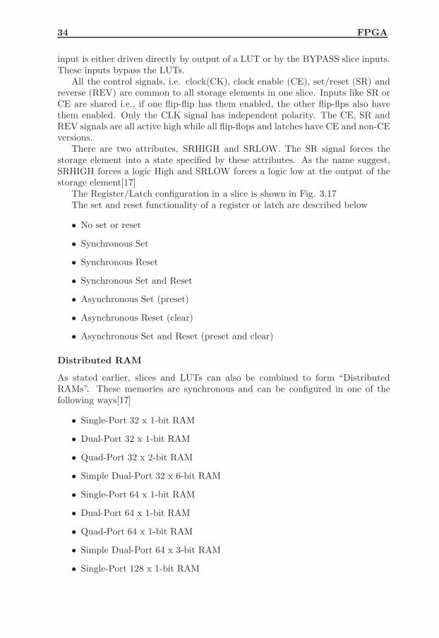
34 FPGA
input is either driven directly by output of a LUT or by the BYPASS slice inputs.These inputs bypass the LUTs.
All the control signals, i.e. clock(CK), clock enable (CE), set/reset (SR) andreverse (REV) are common to all storage elements in one slice. Inputs like SR orCE are shared i.e., if one flip-flip has them enabled, the other flip-flps also havethem enabled. Only the CLK signal has independent polarity. The CE, SR andREV signals are all active high while all flip-flops and latches have CE and non-CEversions.
There are two attributes, SRHIGH and SRLOW. The SR signal forces thestorage element into a state specified by these attributes. As the name suggest,SRHIGH forces a logic High and SRLOW forces a logic low at the output of thestorage element[17]
The Register/Latch configuration in a slice is shown in Fig. 3.17The set and reset functionality of a register or latch are described below
• No set or reset
• Synchronous Set
• Synchronous Reset
• Synchronous Set and Reset
• Asynchronous Set (preset)
• Asynchronous Reset (clear)
• Asynchronous Set and Reset (preset and clear)
Distributed RAM
As stated earlier, slices and LUTs can also be combined to form “DistributedRAMs”. These memories are synchronous and can be configured in one of thefollowing ways[17]
• Single-Port 32 x 1-bit RAM
• Dual-Port 32 x 1-bit RAM
• Quad-Port 32 x 2-bit RAM
• Simple Dual-Port 32 x 6-bit RAM
• Single-Port 64 x 1-bit RAM
• Dual-Port 64 x 1-bit RAM
• Quad-Port 64 x 1-bit RAM
• Simple Dual-Port 64 x 3-bit RAM
• Single-Port 128 x 1-bit RAM

3.10 Xilinx 35
Figure 3.17. Register/Latch configuration in a Slice[17]

36 FPGA
• Dual-Port 128 x 1-bit RAM
• Single-Port 256 x 1-bit RAM
These memories are synchronous write. A synchronous read can also be im-plemented by using the flip-flop in the same slice. This decreases the delay intothe clock-to-out value of the flip but introduces one extra cycle of latency.
The resource utilization of LUTs by each distributed RAM configuration isgiven below[17]
RAM Number of LUTs32 x 1Sa 132 x 1Db 232 x 2Qc 4
32 x 6SDPd 464 x 1S 164 x 1D 264 x 1Q 4
64 x 3SDP 4128 x 1S 2128 x 1D 4256 x 1S 4
aSingle PortbDual PortcQuad PortdSimple Dual Port
Table 3.5. Type of Distributed RAMs
The RAM has a common address port for synchronous writes and asynchronousreads. In case of dual-port configurations, the memory has one port for syn-chronous writes and asynchronous reads and another one for asynchronous reads.For quad-port, there is one port for synchronous writes and reads and three addi-tional port for asynchronous reads[17].
Interested readers are referred to [17] for further details on Distributed RAMs.
Read Only Memory
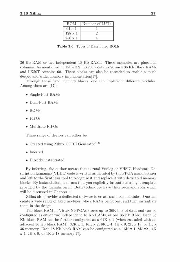
Both SLICEM and SLICEL can implement Read Only Memory. Table 3.6 showsthe types of ROMs and their corresponding resource utilization[17].
Virtex-5 Block RAMs
The Xilinx Virtex-5, in addition to distributed RAMs, has a large number of fixedmemory blocks called block RAMs. Each block RAM can store up to 36K bitsof data and thus referred to as 36 Kb RAM. They can either be utilized as ’1’
3.10 Xilinx 37
ROM Number of LUTs64 x 1 1128 x 1 2256 x 1 4
Table 3.6. Types of Distributed ROMs
36 Kb RAM or two independent 18 Kb RAMs. These memories are placed incolumns. As mentioned in Table 3.2, LX20T contains 26 such 36 Kb Block RAMsand LX50T contains 60. These blocks can also be cascaded to enable a muchdeeper and wider memory implementation[17].
Through these fixed memory blocks, one can implement different modules.Among them are [17]:
• Single-Port RAMs
• Dual-Port RAMs
• ROMs
• FIFOs
• Multirate FIFOs
These range of devices can either be
• Created using Xilinx CORE GeneratorTM
• Inferred
• Directly instantiated
By inferring, the author means that normal Verilog or VHSIC Hardware De-scription Language (VHDL) code is written as dictated by the FPGA manufacturerand left to the Synthesis tool to recognize it and replace it with dedicated memoryblocks. By instantiation, it means that you explicitly instantiate using a templateprovided by the manufacturer. Both techniques have their pros and cons whichwill be discussed in Chapter 4.
Xilinx also provides a dedicated software to create such fixed modules. One cancreate a wide range of fixed modules, block RAMs being one, and then instantiatethem in the design.
The block RAM in Virtex-5 FPGAs stores up to 36K bits of data and can beconfigured as either two independent 18 Kb RAMs, or one 36 Kb RAM. Each 36Kb block RAM can be further configured as a 64K x 1 (when cascaded with anadjacent 36 Kb block RAM), 32K x 1, 16K x 2, 8K x 4, 4K x 9, 2K x 18, or 1K x36 memory. Each 18 Kb block RAM can be configured as a 16K x 1, 8K x2 , 4Kx 4, 2K x 9, or 1K x 18 memory[17].
38 FPGA
The Write and Read are synchronous operations; although the two ports sharethe store data, they are symmetrical and totally independent. Each port can beconfigured in one of the available widths, independent of the other port. Fur-thermore, the read port width can be different from the write port width for eachport. The memory can also be initialized or cleared by the configuration bitstream.During a write operation the memory can be set to have the data output eitherremain unchanged, reflect the new data being written or the previous data nowbeing overwritten[17].
Additional Virtex-5 FPGA block RAM enhancements include[17]:
• Each 36K block RAM can be set to simple dual-port mode, doubling datawidth of the block RAM to 72 bits. The 18K block RAM can also be setto simple dual-port mode, doubling data width to 36 bits. Simple dual-portmode is defined as having one read-only port and one write-only port withindependent clocks.
• One 64-bit Error Correction Coding block is provided per 36 Kb block RAMor 36 Kb First In First Out (FIFO). Separate encode/decode functionalityis available.
• Synchronous Set/Reset of the outputs to an initial value is available for boththe latch and register modes of the block RAM output.
• An attribute to configure the block RAM as a synchronous FIFO to eliminateflag latency uncertainty.
• The Virtex-5 FIFO does not have FULL flag assertion latency.
True Dual Port RAM
The Xilinx Block RAMs are true Dual-Port RAMs. The 36 Kb block RAM hasa 36 Kb storage area. The two ports are completely independent. Same is thecase with the 18 Kb counterpart. The structure is fully symmetrical. Figure 3.18shows the true dual-port block diagram and Table 3.7 list the port definitions[17].
Regarding read and write operation, data can be read/written from either oneor both ports. Both operations are synchronous and require a clock edge. Asevident, each port has its own address, data in, data out, clock, clock enable andwrite enable ports.
Information about different writing modes, timing diagrams and other addi-tional details, please refer to [17].
Virtex-5 Simple Dual Port RAM
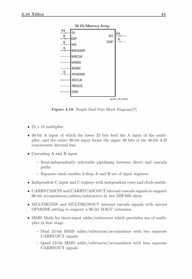
Apart from True Dual Port RAM, the Block RAMs can also be configured asSimple Dual-Port RAMs. The difference is that one port can not be used for bothreading and writing. One port is designated for reading and one for writing thusallowing independent Read and Write operations to happen simultaneously. Figure3.19 shows the simple dual-port data flow[17] and port definitions are available inTable 3.8.

3.10 Xilinx 39
Figure 3.18. True Dual Port[17]
Virtex-5 DSP48E Slice
The DSP48E slice in Virtex-5 is an extension to the DSP48 slice available inVirtex-4 FPGA. These special slices allow special functions to be implemented init without using the FPGA fabric. Many DSP algorithms are supported resultingin low power, high performance and efficient device utilization.
This special slice is a new element in the Xilinx development model referredearlier to as Application Specific Modular Blocks (ASMBLTM ). The purpose ofthis model is to deliver off-the-shelf programmable devices with the best mix oflogic, memory, I/O, processors, clock management and digital signal processing.ASMBL is an efficient FPGA development model for delivering off-the-shelf, flex-ible solutions ideally suited to different application domains[20].
Each DSP tile in Virtex-5 contains two DSP48E Slices and a local interconnectfor connection to other devices and general FPGA fabric[21].
The DSP48E slice support many independent functions like
• Multiplier

40 FPGA
Port Name DescriptionDI[A|B] Data Input BusDIP[A|B] Data Input Parity Bus, can be used for
additional data inputsADDR[A|B] Address BusWE[A|B] Byte-wide Write EnableEN[A|B] When inactive no data is written to the
block RAM and the output bus remainsin its previous state
SSR[A|B] Synchronous Set/Reset for either latchor register modes
CLK[A|B] Clock InputDO[A|B] Data Output BusDOP[A|B] Data Output Parity Bus, can be used
for additional data outputsREGCE[A|B] Output Register EnableCASCADEINLAT[A|B] Cascade input pin for 64K x 1 mode
when optional output registers are notenabled
Table 3.7. True Dual Port Definitions
• Multiply-Accumulate
• Multiply-Add
• Three Input Adder
• Barrel Shifter
• etc
The architecture also supports connection with multiple DSP48E slices toform wide math function, DSP filters and complex arithmetic without involvingthe general-purpose FPGA fabric. In this thesis, the Multiply-Accumulate andMultiply-Add features of the DSP48E slice has bene utilized.
The Virtex-5 DSP48E slice is shown in Fig. 3.20The DSP48E slice has a 25 x 18 multiplier and an add/subtract as its funda-
mental component. This add/subtract function has been extended to also functionas a logic unit. This logic unit performs a number of bitwise logical operationswhen the multiplier is not is use. It also includes a pattern detector and a patternbar detector that can be used for convergent rounding, overflow/underflow de-tection for saturation arithmetic and auto-resetting counters/accumulators. TheSingle Instruction Multiple Data (SIMD) mode of the adder/subtracter/logic unitis also available[21].
The complete list of DSP48E features is available in [21] and reproduced below
3.10 Xilinx 41
Figure 3.19. Simple Dual Port Block Diagram[17]
• 25 x 18 multiplier
• 30-bit A input of which the lower 25 bits feed the A input of the multi-plier, and the entire 30-bit input forms the upper 30 bits of the 48-bit A:Bconcatenate internal bus.
• Cascading A and B input
– Semi-independently selectable pipelining between direct and cascadepaths
– Separate clock enables 2-deep A and B set of input registers
• Independent C input and C register with independent reset and clock enable.
• CARRYCASCIN and CARRYCASCOUT internal cascade signals to support96-bit accumulators/adders/subtracters in two DSP48E slices
• MULTSIGNIN and MULTSIGNOUT internal cascade signals with specialOPMODE setting to support a 96-bit MACC extension
• SIMD Mode for three-input adder/subtracter which precludes use of multi-plier in first stage
– Dual 24-bit SIMD adder/subtracter/accumulator with two separateCARRYOUT signals
– Quad 12-bit SIMD adder/subtracter/accumulator with four separateCARRYOUT signals

42 FPGA
Figure 3.20. DSP48E Slice[17]
3.10 Xilinx 43
Port Name DescriptionDO Data Output BusDOP Data Output Parity BusDI Data Input BusDIP Data Input Parity BusRDADDR Read Data Address BusRDCLK Read Data ClockRDEN Read Port EnableREGCE Output Register Clock EnableSSR Synchronous Set/ResetWE Byte-wide Write EnableWRADDR Write Data Address BusWRCLK Write Data ClockWREN Write Port Enable
Table 3.8. Simple Dual Port Definitions
• 48-bit logic unit
– Bit-wise logic operations - two-input AND, OR, NOT, NAND, NOR,XOR, and XNOR
– Logic unit mode dynamically selectable via ALUMODE
• Pattern detector
– Overflow/underflow support
– Convergent rounding support
– Terminal count detection support and auto resetting
• Cascading 48-bit P bus supports internal low-power adder cascade
– The 48-bit P bus allows for 12-bit/QUAD or 24-bit/DUAL SIMD addercascade support
• Optional 17-bit right shift to enable wider multiplier implementation
• Dynamic user-controlled operating modes
– 7-bit OPMODE control bus provides X, Y, and Z multiplexer selectsignals
• Carry in for the second stage adder
– Support for rounding
– Support for wider add/subtracts
– 3-bit CARRYINSEL multiplexer
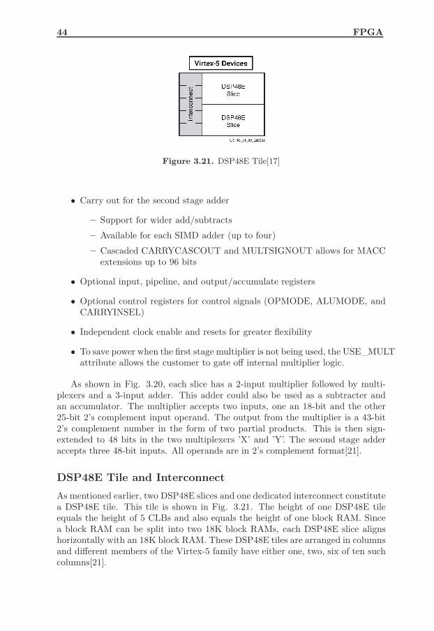
44 FPGA
Figure 3.21. DSP48E Tile[17]
• Carry out for the second stage adder
– Support for wider add/subtracts
– Available for each SIMD adder (up to four)
– Cascaded CARRYCASCOUT and MULTSIGNOUT allows for MACCextensions up to 96 bits
• Optional input, pipeline, and output/accumulate registers
• Optional control registers for control signals (OPMODE, ALUMODE, andCARRYINSEL)
• Independent clock enable and resets for greater flexibility
• To save power when the first stage multiplier is not being used, the USE_MULTattribute allows the customer to gate off internal multiplier logic.
As shown in Fig. 3.20, each slice has a 2-input multiplier followed by multi-plexers and a 3-input adder. This adder could also be used as a subtracter andan accumulator. The multiplier accepts two inputs, one an 18-bit and the other25-bit 2’s complement input operand. The output from the multiplier is a 43-bit2’s complement number in the form of two partial products. This is then sign-extended to 48 bits in the two multiplexers ’X’ and ’Y’. The second stage adderaccepts three 48-bit inputs. All operands are in 2’s complement format[21].
DSP48E Tile and Interconnect
As mentioned earlier, two DSP48E slices and one dedicated interconnect constitutea DSP48E tile. This tile is shown in Fig. 3.21. The height of one DSP48E tileequals the height of 5 CLBs and also equals the height of one block RAM. Sincea block RAM can be split into two 18K block RAMs, each DSP48E slice alignshorizontally with an 18K block RAM. These DSP48E tiles are arranged in columnsand different members of the Virtex-5 family have either one, two, six of ten suchcolumns[21].
3.10 Xilinx 45
DSP48E Slice for FIR Filters
The basic operation in FIR filters is that of multiply and add. Depending upon thetype of implementation, this multiply-add could either be multiply-accumulate oronly multiply-add. The Virtex-5 DSP48E slice contains all the elements requiredfor all these implementations. As evident in earlier text, this slice contains amultiplier followed by an adder. There are also delay or pipeline registers. Theseregisters can be used to have a completely pipelined DSP operation with registersat the input and output of the multiplier and also at the output of the adder.

Chapter 4
Architecture
This chapter describes the two architectures implemented for time-multiplexedFIR filters. As mentioned earlier, time-multiplexing means that the frequency ofinput data is less than the clock frequency. This allows the resources to be re-used.But this also means, that the data within the filter needs to be retained for thenumber of cycles between successive input data.
In a normal, direct-form FIR filter, there are three main components as shownin Fig. 2.4: multiplier, adder and delay line. For non-time-multiplexed FIR filters,these delay line can be either implemented by a shift register or simple delaysbetween multiplications. But since in time-multiplexed FIR filters data need to beretained, memories could be utilized both as Delay Line as well as data retentionunits.
The two architectures explored in this thesis are based on symmetric/anti-symmetric and non-symmetric FIR filters. Although, most of the FIR filters arelinear and thus have symmetric coefficients, it was important to study structuresfor non-symmetric filters. Also important to study was whether implementingsymmetric filters using such architectures which do not exploit symmetry will giveany benefit or not.
The two architectures will be referred with the following names
• Fully Parallel Symmetric FIR Filter
• Semi Parallel Non-Symmetric FIR Filter
For each architecture, ’2’ designs have been implemented. In one, the coef-ficients are of 18 bits. In the other, the coefficients were scaled using the safescaling. This enabled to observe if there was any advantage in scaling the coeffi-cients in terms of resource usage, frequency and power dissipation. Thus, in total,’4’ designs were generated. But before describing each architecture in detail, theDesign Flow employed in this thesis is first presented.
47
48 Architecture
4.1 Design Flow
The Design Flow of the implementation is described in Fig. 4.1. Each step isdescribed below
4.1.1 VHDL - The Chosen HDL
The HDL chosen to implement the whole filter is VHDL. HDL are used to describeelectronic circuits, specially digital logic. It describes circuit’s operation, design,connectivity and also provides structures for efficient verification of the design.There are different programming languages. Programming Languages are usedto program the hardware, where they describe the hardware to be implementedin real sense. Hardware units like adders, registers, flip-flops etc can be directlydescribed in such languages.
VHDL, if compared to its competitor Verilog HDL, is a much more verboseand strongly-typed language. A lot of things have to be written in order to havea workable design. However, there are a lot of advantages. VHDL gives a lotmore control over implementation aspects and provides a lot more constructs forefficient behavioral as well as structural design.
However, VHDL is not directly written in this thesis. The focus of this thesishas been generated of VHDL design using Matlab which is described in the nextsection.
4.1.2 Matlab
As mentioned in the previous section, the design methodology of this thesis hasbeen generation of VHDL design files using Matlab. Matlab is a very powerful tooland is used in many different fields, digital signal processing being one of them.
Generating code using Matlab allows greater flexibility in generating designs fordifferent filter order, time-multiplexing (memory folder factor), data and coefficientword length. Multiple Matlab scripts are used to generate all the design files.These scripts are not very advance Matlab files, mostly they contain a lot of printstatements that are used to generate VHDL code. However, this print statementsare controlled by for loops and if-else statements based on the supplied inputparameters. One Matlab script is used for one design file. Then all the scriptsare combined in one main script which basically acts as the interface to the user.The scripts will be described in detail when each design is explained. However,the interface of these main scripts for all the ’4’ designs is same and requires thefollowing inputs from the user.
• Filter Order
• Time-Multiplexing Factor (referred to as Memory Folding Factor)
• Data Width
• Coefficient Width
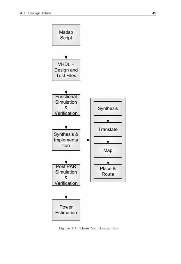
4.1 Design Flow 49
Figure 4.1. Thesis Main Design Flow
50 Architecture
• Number of Test Vectors (for Random Testing)
• Testing Methodology, whether testing is to be ’Random’ or ’Exhaustive’
Most of the inputs are self-explanatory. The final ’2’ inputs are related todesign verification. There are two ways in which the design could be verified, bothat functional level (Register Transfer Level (RTL) Simulation) and Gate Level(Post Place And Route (PAR) Simulation). If the testing methodology is random,then the previous inputs informs the scripts the number of random test vectors tobe generated. If it is exhaustive, then the previous input holds no meaning.
4.1.3 Functional Simulation and Verification
After the Matlab script has generated all the files, the next step is to verify thefunctionality of the RTL design. The Matlab script also generates the test benchand the required .do file. These ’do’ files are ModelSim scripts in Tcl. The ’do’ fileused in this design removes the work directory, compiles all the individual modulesincluding the test-bench and simulates the design.
The test-bench generates data and sends it to both ’Design Under Test (DUT)’and a behavioral model and compares the output of both. A successful simulationmeans that all output data from the main design match that of the model.
4.1.4 Synthesis and Implementation
The next step, after verifying the functionality of the design, was synthesis andimplementation. Synthesis means translating the design from RTL to gate leveland beyond. Since Xilinx FPGAs are the focus of this thesis, synthesis flowas provided by Xilinx is followed. Its graphical tool called Integrated SystemEnvironment (ISE) is used to implement the design on the FPGA. It consists ofthe following steps
• Synthesis
• Translate
• Mapping
• Place and Route
Each step is briefly described below
Synthesis
Synthesis, often referred as logic synthesis or RTL synthesis, is a step where thebehavioral description of the design in a HDL is translated to logic gates. Inthe Xilinx design flow, this step is called Xilinx Synthesis Technology (XST). Ittranslates the HDL code to create Xilinx-specific netlist files called NGC Files.This netlist contains both logical design data and constraints[22].
4.1 Design Flow 51
Translate
The Translate step is commonly known as Native Generic Database (NGD)Build in the Xilinx synthesis and implementation design flow. It reads the NGCfile created by XST and creates the Xilinx NGD file. This file contains the logicaldescription of the design in terms of logic elements like Logic Gates, Decoders,Flip-Flops, RAMs etc. The output of NGD file can be directly mapped to thedesire device family[23].
Mapping
The Mapping (MAP) is a step where the design is mapped to different components,like logic cells, I/O cells etc, in the target Xilinx FPGA. Map first performs a logicalDesign Rule Check (DRC) on the NGD file and then performs this mapping. Theoutput from this step is a Native Circuit Description (NCD) file[23]. This file isused in the next step PAR
Place and Route
The PAR step accepts the NCD file generated by the MAP and places and routesthat design on the target FPGA. The file it produces is also an NCD file andis used by the bitstream generator (BitGen). There are two considerations inPAR[23]
1. Timing Driven - PAR is performed based upon timing constraints
2. Non-Timing Drive - PAR is performed using various cost tables that assignweighted values to relevant factors such as constraints and available routingresources. Such PAR is performed when there are no timing constraints.
The PAR tool places the components into areas based on constraints, lengthof connections and the available routing resources. After this, the router routesthe design to completion so that the timing constraints are met. Once the designis fully routed, PAR writes an NCD file which can be analyzed for timing.
4.1.5 Post PAR Simulation and Verification
It was important to verify the functionality of the filter after the design has beencompletely mapped, placed and routed on the target FPGA. This purpose is servedby performing Post Place and Route Simulation. Xilinx provides an applicationcalled NetGen which reads design files as input and produces netlists that can bethen simulated using appropriate simulators.
For this design, this application reads the NCD file from PAR and producesSIMPRIM-based netlist along with a full timing sdf file. Simulation of this filerequire SIMPRIM library, a library having definitions for the placed and routedcomponents. The whole design is contained in one file and only this file needs tobe simulated. This file was simulated using a test bench generated by Matlab. Theprocedure was same as highlighted in Section 4.1.3. This simulation was also used

52 Architecture
to generate a file called VCD file which was generated by the ModelSim simulator.This file is used by the Xilinx power estimation tool.
4.1.6 Power Estimation
The last step in the design cycle adopted in thesis was power estimation. Lowpower is the mantra of today. The need for electronic products to be smaller, fasterand having a long battery life, has put a lot of strain on the power consumption ofsuch devices. So it is imperative that power consumption of devices being designedcan be estimated accurately early in the design phase.
Xilinx provides a tool, called Xpower which provides power and thermal esti-mates for FPGA after PAR. It does the following[23]
• Estimates how much power the design will consume
• Identifies how much power each net or logic element in the design is consum-ing
• Verifies that junction temperature limits are not exceeded
Xpower uses three files to provide the power estimates[23]:
• NCD file generated by PAR. Details about this file available in Section 4.1.4.
• Physical Constrant File (PCF) which contains timing constraints.
• Value Change Dump (VCD) file. This file was generated by ModelSim duringpost place and route simulation. It uses this file to set frequencies andactivity rates of internal signals.
Starting from the next section, each design is explained in detail.
4.2 Architecture - 1 : Fully Parallel SymmetricFIR Filter
4.2.1 Basic Idea
It has been repeatedly mentioned earlier in this chapter, that the designs exploredin this thesis contains a memory which is used both to hold the data betweensuccessive data arrivals and also to model the delay line we find in direct-form FIRfilter structures. Thus, the basic idea revolves around the memory and movementof data.
Figure 4.2 shows how data is arranged in memories. Each memory is arrangedas a Circular Buffer. This means that the new data arriving is always stored inthe first memory while the last data in each memory is then moved to the nextmemory. This movement of data across memories model one part of the delayline. The other part of delay line is data movement within a memory. This is
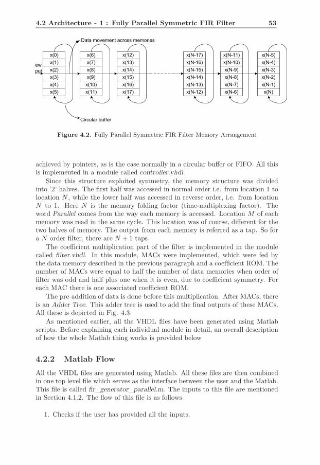
4.2 Architecture - 1 : Fully Parallel Symmetric FIR Filter 53
Figure 4.2. Fully Parallel Symmetric FIR Filter Memory Arrangement
achieved by pointers, as is the case normally in a circular buffer or FIFO. All thisis implemented in a module called controller.vhdl.
Since this structure exploited symmetry, the memory structure was dividedinto ’2’ halves. The first half was accessed in normal order i.e. from location 1 tolocation N , while the lower half was accessed in reverse order, i.e. from locationN to 1. Here N is the memory folding factor (time-multiplexing factor). Theword Parallel comes from the way each memory is accessed. Location M of eachmemory was read in the same cycle. This location was of course, different for thetwo halves of memory. The output from each memory is referred as a tap. So fora N order filter, there are N + 1 taps.
The coefficient multiplication part of the filter is implemented in the modulecalled filter.vhdl. In this module, MACs were implemented, which were fed bythe data memory described in the previous paragraph and a coefficient ROM. Thenumber of MACs were equal to half the number of data memories when order offilter was odd and half plus one when it is even, due to coefficient symmetry. Foreach MAC there is one associated coefficient ROM.
The pre-addition of data is done before this multiplication. After MACs, thereis an Adder Tree. This adder tree is used to add the final outputs of these MACs.All these is depicted in Fig. 4.3
As mentioned earlier, all the VHDL files have been generated using Matlabscripts. Before explaining each individual module in detail, an overall descriptionof how the whole Matlab thing works is provided below
4.2.2 Matlab Flow
All the VHDL files are generated using Matlab. All these files are then combinedin one top level file which serves as the interface between the user and the Matlab.This file is called fir_generator_parallel.m. The inputs to this file are mentionedin Section 4.1.2. The flow of this file is as follows
1. Checks if the user has provided all the inputs.

54 Architecture
Figure 4.3. Fully Parallel Symmetric FIR Filter Block Diagram
4.2 Architecture - 1 : Fully Parallel Symmetric FIR Filter 55
2. Checks if the user has provided the correct values for the filter order andmemory folding factor. There are two criteria for correct values.
(a) The Filter order and memory folding factor should result in Even num-ber of memories. This is done so that symmetry can be exploited.
(b) In case of filter order being ’even’, the filter order should be integermultiple of the memory folding factor.
In both the cases, if the input is not correct, the Matlab scripts prints amessage and execution of the script is aborted. Both of these conditions arealso checked in each individual module.
3. Based on the filter order, coefficients are generated.
4. If coefficients are to be scaled, they are passed on to a script called scaling.m
5. If coefficients are to be scaled, internal data widths are determined.
6. All coefficients, that were calculated as integers, are converted to 2’s com-plement binary numbers, so that they can be used to generate coefficientROMs.
7. Coefficient ROMs Addresses were calculated
8. COE files are generated that is used for the FIR Compiler generated byCoregen of Xilinx.
9. All the individual VHDL files are generated using individual scripts
10. Also created are simulation files both for functional simulation and post PARsimulation
11. Test benches for function simulation and post PAR simulation of design andpost PAR simulation of FIR compiler are also generated
12. Coefficients ROMs are generated with their respective contents.
13. In each individual script, the header is generated i.e. the IEEE librariesrequired by VHDL code.
All the individual modules implemented and scripts generating them are ex-plained next. The pictorial view of these modules and their connections are shownin Fig. 4.4
4.2.3 FIR Top
This is the top level module named fir_parallel_top.vhdl. It is generated by theMatlab file write_fir_top.m. Two modules are instantiated in this module.
• Controller

56 Architecture
Figure 4.4. Fully Parallel Symmetric FIR Filter Module Connections
4.2 Architecture - 1 : Fully Parallel Symmetric FIR Filter 57
• Filter
There is no computation in this module. In the Matlab script, the importantthing in correctly generating the interface of the two modules. The important partof these interfaces are the outputs of the data memory and coefficient memory. Fora filter order N and memory folding factor M , there are K data memory outputsand K/2 coefficient memory outputs where
K = ⌈N/M⌉ (4.1)
The data memory outputs are named as tapsn and coefficient memory outputsare named as coefm, n and m being having the range 0 to K− 1 and 0 to K/2− 1respectively.
The two instantiated modules are explained next.
4.2.4 Main Controller
The VHDL file for this module is named controller.vhdl, generated from the filewrite_controller.m. This module is responsible for storing the new data in thedata memory and reading the correct data and coefficient from the data memoriesand coefficient memories respectively.
The Matlab Script
The inputs to this script are
• Filter Order
• Memory Folding Factor
• Data Width
• In case of scaling, width of coefficients at each node, else coefficient width
By each node, it is meant each coefficient memory. When scaling is imple-mented, the width of all coefficients within one coefficient ROM is same. Whenthere is no scaling, width of all coefficients is same i.e. 18-bits. Thus, node coeffi-cient width means the width of coefficients in one particular memory.
The script, after its initial procedures of checking validity of inputs, calculatesa few important variables. These variables control the number of data memories,the depth of each memory, number of taps and address width of each memory.
The formulation of these variables in given in Equation 4.2 for even order filtersand in Equation 4.3 for odd order filters
MemoryCount(MC) = N/MTapCount(TC) = N/M + 1MemoryDepth(MD) =MAddressWidth(AW ) = ⌈log2(mem_ff)⌉
(4.2)

58 Architecture
MemoryCount(MC) = (N + 1)/MTapCount(TC) = (N + 1)/MMemoryDepth(MD) =MAddressWidth(AW ) = ⌈log2(mem_ff)⌉
(4.3)
where N is the filter order and M is the memory folding factor.Based on the inputs and these variables, the VHDL code is generated including
port definition, control logic and instantiation of the data and coefficient memories.
The Design
The controller implements the control logic of the filter. The control logic revolvesaround data and coefficient movement. The control cycle starts when new dataarrives and ends when all the data in the memories have been read.
To exploit the symmetry, the data memory is split in two halves. This isbecause, due to symmetry, first half of data i.e. from x(n) to x(n − ⌈N/2⌉ − 1)share the same coefficient with the next half i.e. from x(n−⌊N/2⌋+1) to x(n−N)where N is the filter order. Thus they are added before being multiplied. Thisreduces the number of multiplications by half. Thus it is necessary that these setsof ’2’ data are read at the same time.
Since there are ⌈N/M⌉ memories as shown in Equations 4.2 and 4.3, the firsthalf of data is stored in the first MD/2 memories and next half is stored in thenext MD/2 memories. In the case of filter order being even, there is one extratap, the middle one, that does not share coefficient with any other tap. For this,a small flop is implemented, which sits in between the two halves of memories.Based on the inputs, the script automatically generates this flip-flop.
Both of these arrangements are shown in Figs. 4.5 and 4.6. As shown in bothfigures, new data is always written in the first memory. True-Dual Port memoriesare required as the data movement requires reading and writing at the same time.Port A is used for reading and Port B is used for writing. However, reading andwriting could be done using any port as both ports are readable and writable.Thus, the write enables of Port ’A’ of all memories is grounded.
The writing of this data and movement of data, both within one memory andacross memories, is controlled by the following main things
• ’2’ read pointers
• ’2’ read counters
• ’1’ read address enable
• ’1’ write pointer
• ’1’ write address enable
• ’1’ coefficient address counter
• ’1’ coefficient address enable
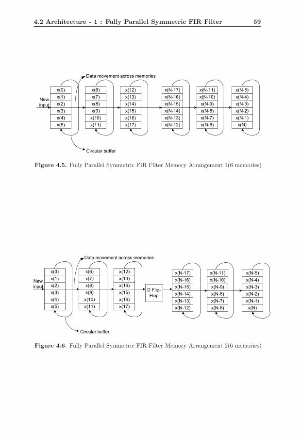
4.2 Architecture - 1 : Fully Parallel Symmetric FIR Filter 59
Figure 4.5. Fully Parallel Symmetric FIR Filter Memory Arrangement 1(6 memories)
Figure 4.6. Fully Parallel Symmetric FIR Filter Memory Arrangement 2(6 memories)

60 Architecture
• ’1’ tap enable
Each of the read pointers and counters are used for each half. This is becausereading pattern of the two halves is different. First half is read in reverse order andsecond half read in straight order. Only one read enable is required because bothmemories need to be read for the same number of clock cycles. Data is writtenfirst to location 0 and then the write pointer is incremented by 1. Thus order ofwriting is from 0 to MD. Furthermore, data is always written to the place whichholds the oldest data in that memory. In the first half of memory, latest datawritten is read first and then the next latest data is read. This means that, say forfilter order 15 and memory folding factor 4, the first data is written on location 0replacing the oldest data and the next to oldest data is present in location 1 andnext to latest data is in location 1. Thus the reading order is 0, 3, 2, 1. This is thereading order of the first half. To exploit symmetry, the first data is to be addedto the last data. Thus in the second half, last data in each memory needs to beread to accomplish this. This would mean that for the given example, the readingorder for the second half is 1, 2, 3, 0. This is how data movement is controlledwithin a memory. Data does not move, only pointer update takes place.
This pointer update happens in the following way. When data has been written,say to location 0, the write pointer increments to point to location 1 to indicate thenew position of writing. For reading the data in the correct order, it is necessaryto indicate the location from where reading should start. As mentioned in theprevious paragraph, the first reading order for the upper half is 0, 3, 2, 1. Nowwhen the next data arrives, the oldest data is in location 1, so the new readingorder is 1, 0, 3, 2. So the read pointer increments on every new data arrival and theread counter, for every new read cycle, takes this value and then is decrementedon every clock cycle. Same happens for the second half of memory. After the readcycle of 1, 2, 3, 0, the next read cycle is 2, 3, 0, 1. These read cycles continue as longas new data keeps on arriving.
For data movement across memories, the oldest data in any memory needsto be moved to the next memory. The oldest data in the last memory is thendiscarded. This achieves the emulation of a delay line where the last data isalways discarded. This is done by using the write pointer and the write port ofport B of the memories. Although port B is not used for reading, its output portwould always show the contents of the location the current address is pointing to.So when writing to a particular address, the output port contains the old data inthat location. Since writing is synchronous, the internal contents of the memory isnot updated immediately in that cycle. Furthermore, the data being overwritten isthe oldest data, this data needs to be moved to the next memory. This movementis simply obtained by connecting the output of port B to the input of port B ofthe next memory. Thus, when new data arrives, the old data of all the memoriesare available at the output and all data movement happens in once cycle.
It is quite clear from the above description that for every new input, writingtakes only one cycle for all memories. No further data movement takes place.Only pointer update is required to read all the new data, minimizing the switchingactivity considerably.

4.2 Architecture - 1 : Fully Parallel Symmetric FIR Filter 61
There is just one exception to the flow described above when the filter order iseven. For even order filter, the number of taps is odd. So there is one extra tap thatonly needs to be multiplied by just one coefficient, the central tap. This centraltap is saved in a flip-flop which resides in between the two halves of memories.This extra flip-flop is shown in Fig. 4.6. When the oldest data is being read fromthe last memory of the first half, it is written to this flop and the old data in thisflop is written to the first memory of the second half. Thus this flip-flop acts asa small, single location memory. This flip-flop also acts as the middle output tap.This arrangement helps in keeping the architecture symmetric, still the design hadtwo separate halves of memories and access pattern remains same.
Coefficient reading from ROMs is a straight forward affair. It only needs tobe read in one direction, always starting from location 0 and going until the lastlocation. The division of coefficients in the ROM maps to the data division. Thememory count variable in Equations 4.2 and 4.3 applies to both memories. Whennew data arrives, all the coefficients in the ROM are read, one from each ROM inone cycle. Coefficient address enable is used to enable this counter.
To qualify the output from data memory, a tap valid signal is generated. Sincereading from memory takes one cycle, the read enable signal, the signal whichenables both the read counters, is used to generate this signal.
4.2.5 Data Memory
The Data Memory is implemented in the module named datamem.vhdl. This file isgenerated by the Matlab file writedatamem.m. This module implements the datamemory. It instantiates all the individual block RAMs used as data memories.
The Matlab Script
The script is simple. It takes filter order, memory folding factor and data widthas the input. The two variables that control the generating of VHDL code is theaddress width of all memories and memory count. These variables are same as inEquations 4.2 and 4.3. The instantiations are done using a for-loop.
The Design
The design is pretty straight forward. Only instantiations, no computations. Thereis only one component of a RAM which is instantiated multiple times. As indi-cated in Section 4.2.4, dual port memories are used. The ram component is alsogenerated using Matlab script.
Block RAM
The basic RAM component Matlab script takes in the filter order, memory foldingfactor and data width as its inputs. The address width is determined by the filterorder and memory folding factor as shown in Equations 4.2 and 4.3. As wasmentioned in Section 3.10.1 in the subsection of block RAMs, there are three waysof designing these blocks rams. Among the three mentioned, memory inference was
62 Architecture
selected as the method of implementation. Generating memory core using Xilinxcore generator was out of option as every VHDL file had to be generated usingMatlab script. Instantiation a block RAM using the primitive provided by Xilinxrequired a lot of code to be written. Also, the primitive requires a 14-bit addresswhile the required address width changed with filter order and memory foldingfactor. Memory inference means writing code using always blocks as directed by[23].
For true dual port rams, ’2’ always blocks are used, one for each port. Bothports have their own port for clock, so while instantiating each RAM, same clockis provided to both ports. In case, same memory location is accessed for readingand writing in the same port, old data is read out from the output port. In casesame memory location is accessed for reading in one port and writing in the otherport, Xilinx says that old data would be read out. However it was found, whileimplementing the second architecture, that this is not always true. Thus it is bestto avoid such a collision. The behavior is uncertain when the same location isbeing written using different ports.
4.2.6 Coefficient Memory
The module name for this is coef_mem.vhdl and the name of Matlab script iswrite_coef_mem.m. The coefficient memory consists of a number of differentROMs equal to the memory count described in Equations 4.2 and 4.3. EachROM is a separate component because the contents of each one is different. Sim-ple, single port, distributed memories are utilized to create these ROMs. Theindividual ROMs are also generated by Matlab script, where the parent scriptfir_generator_parallel.m supplies the right coefficients in the correct order whencalling the Matlab script creating these ROMs. This module only has instantia-tions and no computations.
The Matlab Script
It is nearly the same as in Section 4.2.5. It takes in filter order, memory foldingfactor and the data width of the coefficients to be stored in one ROM. This width issame for all coefficients in the unscaled version while each memory has a differentwidth in the scaled one. The script calculates the same address width and memorycount as before. First it generates code for component declaration and then codefor component instantiation.
There is just a slight difference between even and odd filters. For even orderfilters, the extra tap needs to be multiplied with only ’1’ coefficient. This ’1’ extracoefficient is stored in a single flop which is named mid_coef_flop. It can beconsidered as a ’1’ location ROM generated by its own script.
The Design
The design is not complex. It only instantiates the required ROMs. The ROMsare implemented as distributed.

4.2 Architecture - 1 : Fully Parallel Symmetric FIR Filter 63
Distributed ROM
The coefficient memory consists of ROMs. These ROMs, unlike block RAMs indata memory, are distributed memories. By distributed, one means that thesememories are implemented using general FPGA fabric i.e. slices and LUTs. Thereason is that these memories are simple, single port memories which can be easilyimplemented using the general logic while leaving Block RAMs is left for datamemories and other memories if this filter is part of a larger system. The scriptgenerating these ROMs takes in the addresses for each rom which are named asinputs, the coefficients named as outputs and the name of the ROM which is astring. This module is taken from the supervisor and changed slightly so that onecan have synchronous memories. The name attribute is important as, based onthe variable memory count, a number of coefficient ROMs need to be implementedwith different contents and thus different names as well. Individual ROMs areinstantiated in the module coef_mem.vhdl with their correct names. Each ROM isimplemented using select statements and, as stated earlier, synchronous in nature.
Scaling
Scaling involves shortening the width of the coefficients to discard those bits whichare just sign-extension bits. This scaling of width would then also reduce theoutput width of the multipliers and would help in determining whether scalingeffects resource utilization, power dissipation and operating frequency.
Safe scaling criteria was used. Scaling was done using Matlab script named scal-ing.m. It was provided a set of coefficients. Each set means coefficients belonging toone coefficient memory. The script was also provided the coefficient width of the co-efficient set. As in safe scaling, absolute sum of the coefficients was calculated andconverted to 2’s complement binary number. The closest number to this calculatedvalue, which is also larger and is a power of ’2’, is found which dictates the pointfrom where coefficient bits need to be selected. For example, consider 8 coefficients(−0.2837,−0.2903, 0.3012, 0.3166,−0.3368,−0.3619, 0.3921, 0.427)× 10−3, the ab-solute sum of which is 0.0027. Binary value, in 18 bits, is 000000000101100011.Thus the coefficients in this node should be at least 10 bits. Thus the initial 8 bitswere discarded as they were only sign extensions. Coefficients for all memorieswere scaled in the same manner.
4.2.7 Main Filter
This is the module where the main filter operation, i.e., pre-addition, multiply-accumulate and final addition is performed. The general structure of the filter isshown in Fig. 4.7. The file name is filter.vhdl and the script generating is namedwrite_fir_filter.m.
The Matlab Script
The Matlab script takes in the following inputs‘
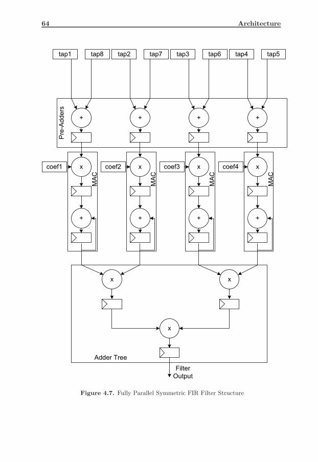
64 Architecture
Figure 4.7. Fully Parallel Symmetric FIR Filter Structure
4.2 Architecture - 1 : Fully Parallel Symmetric FIR Filter 65
• Filter order
• Memory Folding Factor
• Data Width
• Coefficient Width or an array with different coefficient widths for each nodein case of scaled coefficients
• Output data width of MAC
• Data width of the Pre-Adder outputs
• Data width at different nodes of the adder tree
• Final output width
The pre-adder width is 1-bit more than the data width. This is done to ensureno overlow/underflow occurs when large positive or negative numbers are added.In case of unscaled version, MAC output width is coefficient width plus pre-adderwidth and output width is the MAC output width plus the levels of adder treedata has to pass. This will be explained in detail in Section 4.2.10. The finaloutput width is the width of the last level of this adder tree.
Three variables, tap_count, mac_count, mem_count help in different ways tocorrectly generate the VHDL code for different filter orders and memory foldingfactors. These variables are shown in Equations 4.4 and 4.5 for even and odd orderfilters respectively
tap_count = order/mem_ff + 1mac_count = ⌈tap_count/2⌉mem_count = order/mem_ff
(4.4)
tap_count = (order + 1)/mem_ffmac_count = tap_count/2mem_count = (order + 1)/mem_ff
(4.5)
As expected, the number of taps equal the number of memories when filterorder is odd and greater by 1 when it is even. The variable tap_count helps inhelps in generating code related to the taps(data outputs of memories) that aregenerated by controller. Variable mac_count controls code related to declaration,instantiation and signals of MACs and mem_count controls a lot of things likepre-addition, assigning the right coefficient width to the right wire etc.
The Design
This module contains the pre-adders, macs and the adder tree. Pre-adders addthose data which are to be multiplied with the same coefficient, MACs performthe convolution function and the adder tree adds the output of the MACs. Flowis as follows:
• Pre-Adders add the taps together due to symmetry
66 Architecture
• Coefficients are delayed by one cycle to accommodate the cycle cost of thepre-adders
• If filter order is even, there is one extra tap that is not to be added. It isdelayed by one cycle to accommodate the pre-adder cycle cost of 1
• Tap Valids acts as qualifying signals for the taps and used to identify whenvalid data is available for addition
• MAC enables are generated from pre-adder enables
• Data is passed to MACs
• Output of all the MACs is passed to the adder tree. The MACs producetheir own output valids which is then used by the adder tree to qualify theinputs.
4.2.8 Pre-Adder
The pre-adder adds pairs of data that are to be multiplied with the same coefficientas dictated by coefficient symmetry. It is a simple, synchronous adder taking onecycle to add data. The output of the pre-adder is 1 bit more than the inputs toavoid overflow/underflow. The inputs are sign extended to perform this addition.The Matlab script is simple and does not need any variable for any manipulation.It only take the input width and output width as inputs. Design name is add.vhdland script name is write_add.m.
4.2.9 Multiply-Accumulate (MAC)
Multiply-Accumulate is the most important component of an FIR filter design. Itis this that implements the convolution operation of the filter. The design namemac.vhdl and script name is write_mac.vhdl.
The Matlab Script
The Matlab script takes in the filter order, memory folding factor, input datawidth, input coefficient width and output width as its inputs. The filter order andmemory folding factor are required to calculate the number of cycles for whichMACs need to accumulate data and the point where the accumulator needs tobe cleared. For memory folding factor M , the MAC needs to keep on accumulat-ing the multiplication output for M cycles. This requires a counter of ⌈log2M⌉bits. The Matlab script generates code for this counter, multiply, accumulate andaccumulator enable and output valid.
The Design
There are a total of ’5’ synchronous processes. One is counter, one for multiplier,one for accumulator, one for accumulator enable and one for output valid. ’1’MAC operation takes ’2’ cycles. Both the mutiply and accumulate operation are

4.2 Architecture - 1 : Fully Parallel Symmetric FIR Filter 67
registered. The Multiply operation is performed when the input enable is set. Forthe first output of the multiplier, the accumulator does not add up anything. Thisis indicated when the counter is at its initial position. After this, the accumulatorkeeps on accumulating until, as indicated before, counter counts M cycles. Theoutput enable is produced when we the counter has finished counting. On this thecounter is reset and this process is repeated again.
4.2.10 Adder Tree
This is the final stage of the filter. This adder tree is used to add the outputof the MACs. This was one of the most complex designs due to a large numberof possibilities. Initially the aim was to come up with some sort of a formula todetermine the number of stages in the adder tree, the number of add operations ineach node etc. However, formula for only the number of stages was derived. Otherthings were not based on formulas, rather computations. The design is simple, anadder tree with a finite number of stages with finite number of adds in each stage.The adder tree keeps on adding until all inputs are not consumed. However, thescript is quite complex.
The Matlab Script
This was the most complex generation encountered in the whole design. The addertree required determining the number of MAC outputs (an easy task), generationof the correct number of adders per stage based on the number of MAC outputsconsumed (for first stage) and number of consumed outputs of the previous stageof adder tree (for adders in the following stages), data widths at each stage fordifferent adders, number of new data produced, number of old data not consumedand getting them to next stage (the difficult part).
The script calculates the same variable as defined in Equations 4.4 and 4.5.The number of stages is determined as shown in Equation 4.6
No of stages = ⌈log2mac_count⌉ (4.6)
Two arrays are initialized. One indicating the number of adders in each stagewhile one indicating the number of nodes in each stage. Nodes are the outputsof each adder. The calculation of total number of adders in each stage has thefollowing flow
• Nodes per stage is initialized to the number of macs
• Some variables are also initialized which will indicate the number of nodesconsumed, produced and left
• The loop repeatedly checks if the number of nodes is even or not
• If it is even, all produces nodes will be consumed, if not, then ’1’ node willbe left

68 Architecture
• The number of nodes available for each stage is saved in the correspondingarray
• Produced nodes will always be half to that of consumed, each adder is a ’2’input adder
• Nodes per stage is updated. The new nodes for the next stage is the numberof nodes produced plus if any left
• The total number of produced nodes indicate the number of adders
After this, the adders are initialized. Those nodes that will not be consumedin one stage are delayed to account for the cycle cost of that stage. All adders aresynchronous i.e. each stage takes one cycle. For the first stage adders, input validsare used as qualifying signals. However, for other stages, valids are also generated.Since it is known that each stage would take one cycle, it is easy to do so. For thenon-scaled coefficients, the data width increases by ’1’ for each stage. However,in the scaled version, care needs to be taken the output width of each adder. Ifthe input width of the two inputs to any adder are same, the output width is signextended by ’1’, but if they are different, there is no need to increase the width.Output width is the maximum of the two.
There is a special case when there are no adders in the adder tree. That casearises when the filter order is odd and there are only two memories. This happenswhen the time-multiplexing factor (memory folding factor) is half of the filterorder. For such a case, there is only one MAC and thus no need for any addertree. In this case, the adder tree just passes the inputs to the outputs and thescript does not generate any adders.
Adders
The adders in this adder tree are simple, single cycle adders. In the non-scaledversion, the output of the adder is 1 bit more than the inputs. In the scaledversion, however, the output width is either 1 bit more in case of identical wordlength of the inputs or maximum of the two input word lengths. Therefore, in thenon-scaled version the same adder that was used for pre-adders was used. Butfor the scaled version, a different script is used to generate the adders which canproperly control the word lengths as described above. The new adder is namedadd_nodeJK, where J represents the stage within the adder tree andK representsthe adder in that stage. The Matlab script generating is called write_add_node.m.
4.2.11 Functional Simulation
The whole filter was thoroughly tested for a number filter orders and memoryfolding factors. A simple behavioral model was also generated for the same filterorder. This behavioral model was a simple direct form filter consisting of mul-tiplications and registers. The test bench was also automatically generated by aMatlab script. The test bench instantiated both the models and the main filter.The flow of the test bench is as follows
4.2 Architecture - 1 : Fully Parallel Symmetric FIR Filter 69
• All the memories are cleared by passing zeros. The number of zeros equalthe filter order
• If the test is an exhaustive test, a total of 2datawordlength inputs are generated.For random testing, the user provides input for total numbers of test vectorsto be generated
• After all inputs have been generated, zeros are injected to shift out all thedata from the memory
• The output of the model is saved in an array of vector.
• The test bench waits till the filter starts producing proper outputs, as ini-tially only zeros are produced to zero input vectors
• When proper outputs are produced, they are immediately compared to theoutput of the model, the test bench s immediately stopped
• If no mismatch occurs, the test bench displays a message indicating so
One problem with VHDL is that there is no clean way of stopping the simula-tion and ModelSim. Verilog HDL provides a very clean way in $stop and $finish.In VHDL, one needs to force an assertion failure if simulation needs to be stopped.This is exatly what has been implemented. After all outputs have been matched,an assertions is forced to fail, with the error severity level of failure and a messagedisplayed. Only a failure severity level can stop the simulation.
The .do script (Tcl), required by ModelSim to automatically run the simulationwas also generated using Matlab. It removed the simulation directory, created anew one, compiled all the files and ran the simulation. The command for compilingthe VHDL files is vcom -93 -novopt mydesign.vhdl and the command for runningthe simulation is vsim -novopt -do work.topleveldesign wave.do. Top Level isnormally the test bench, wave file is a file which contains all the input/output andinternal signals of the design. The .do script was executed by running vsim -dosim.do.
4.2.12 Synthesis and Implementation
The design was then synthesized and implemented using Xilinx ISE software. Allthe details are available in Section 4.1.4.
4.2.13 Post PAR Simulation
Post PAR simulation model was generated using ISE. That simulation model wasinstantiated in a test bench and the results of this simulation model was againcompared to the same behavioral model as described in Section 4.2.11. However,the test bench was different to the one described in Section 4.2.11, because theRTL contained generics, but the simulation model does not contain them. So aseparate, albeit similar, test bench was generated using Matlab. Also, a separate,.do script was also generated. For more details, refer to Section 4.1.5.

70 Architecture
4.2.14 Power Estimation
In the post PAR simulation, the VCD file generated by ModelSim was used toestimate power. For more details, refer to Section 4.1.6.
4.2.15 Xilinx FIR Compiler
Xilinx provides a complete, time-multiplexed FIR generator called FIR Compler.It is part of Xilinx Core Generator. The compiler provides a a .vhd file for simu-lation and an .ngc file for implementation. This NGC file is a synthesized netlist,which goes throught the same process as highlighted in Section 4.1.4.
The compiler needs the following inputs from the user to generate the core
1. A coefficient file (.coe)
2. Single Rate or Multi-Rate filter
3. Input Sampling Frequency
4. Clock Frequency
5. Coefficient Structure (Symmetric/Non Symmetric)
6. Coefficient Type (Signed/Un-signed)
7. Coefficient Width
8. Input Data Type (Signed/Un-signed)
9. Input Data Width
10. Output Rounding Mode
11. Optimization Goal (Area/Speed)
12. Control Options
13. Data Buffer(Memory) Type (Block/Distributed/Automatic)
14. Coefficient Buffer(Memory) Type (Block/Distributed/Automatic)
15. Input Buffer Type (Block/Distributed/Automatic)
16. Output Buffer Type (Block/Distributed/Automatic)
17. Preference for other storage (Block/Distributed/Automatic)
Default settings were selected for options number 10, 15, 16, 17. The radix ofthe coefficients in the coefficient file is defined as binary and binary coefficientsare provided. The format of the file is given in Fig. 4.8. This coefficient filewas also generated by a Matlab script. Obviously, this filter was supposed to be aSingle Rate Filter. The input sampling frequency and clock frequency was changedfor different test cases and reflected the time-multiplexing factor. The coefficient
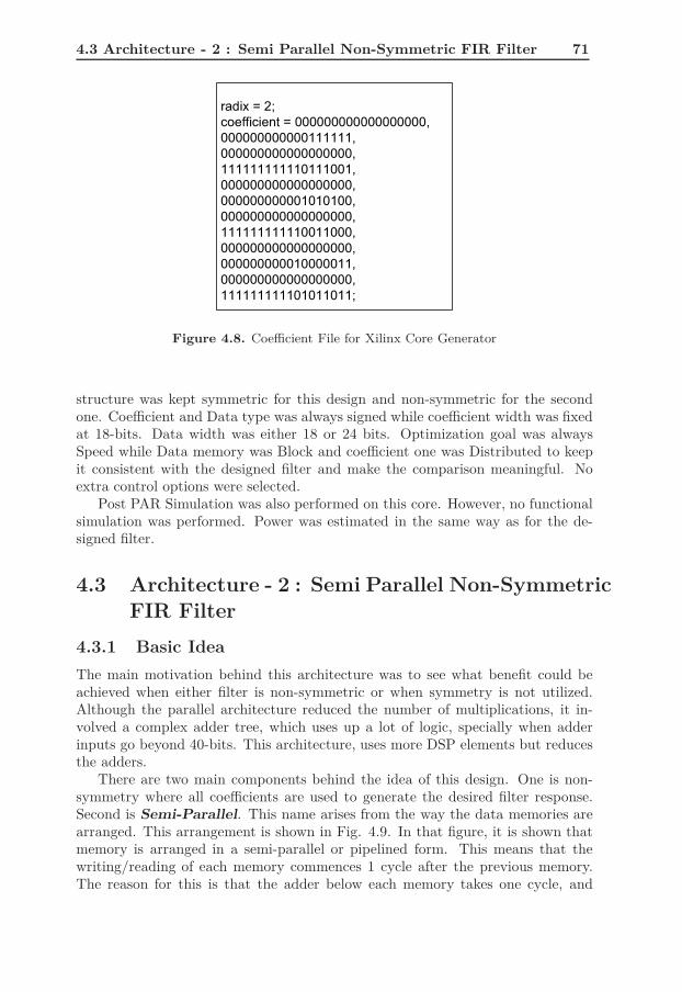
4.3 Architecture - 2 : Semi Parallel Non-Symmetric FIR Filter 71
Figure 4.8. Coefficient File for Xilinx Core Generator
structure was kept symmetric for this design and non-symmetric for the secondone. Coefficient and Data type was always signed while coefficient width was fixedat 18-bits. Data width was either 18 or 24 bits. Optimization goal was alwaysSpeed while Data memory was Block and coefficient one was Distributed to keepit consistent with the designed filter and make the comparison meaningful. Noextra control options were selected.
Post PAR Simulation was also performed on this core. However, no functionalsimulation was performed. Power was estimated in the same way as for the de-signed filter.
4.3 Architecture - 2 : Semi Parallel Non-SymmetricFIR Filter
4.3.1 Basic Idea
The main motivation behind this architecture was to see what benefit could beachieved when either filter is non-symmetric or when symmetry is not utilized.Although the parallel architecture reduced the number of multiplications, it in-volved a complex adder tree, which uses up a lot of logic, specially when adderinputs go beyond 40-bits. This architecture, uses more DSP elements but reducesthe adders.
There are two main components behind the idea of this design. One is non-symmetry where all coefficients are used to generate the desired filter response.Second is Semi-Parallel. This name arises from the way the data memories arearranged. This arrangement is shown in Fig. 4.9. In that figure, it is shown thatmemory is arranged in a semi-parallel or pipelined form. This means that thewriting/reading of each memory commences 1 cycle after the previous memory.The reason for this is that the adder below each memory takes one cycle, and
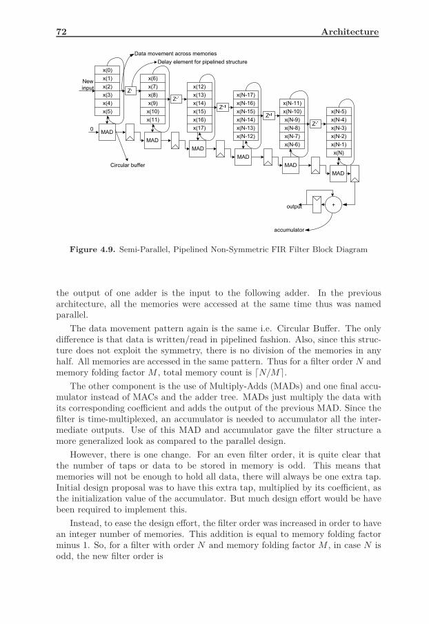
72 Architecture
Figure 4.9. Semi-Parallel, Pipelined Non-Symmetric FIR Filter Block Diagram
the output of one adder is the input to the following adder. In the previousarchitecture, all the memories were accessed at the same time thus was namedparallel.
The data movement pattern again is the same i.e. Circular Buffer. The onlydifference is that data is written/read in pipelined fashion. Also, since this struc-ture does not exploit the symmetry, there is no division of the memories in anyhalf. All memories are accessed in the same pattern. Thus for a filter order N andmemory folding factor M , total memory count is ⌈N/M⌉.
The other component is the use of Multiply-Adds (MADs) and one final accu-mulator instead of MACs and the adder tree. MADs just multiply the data withits corresponding coefficient and adds the output of the previous MAD. Since thefilter is time-multiplexed, an accumulator is needed to accumulator all the inter-mediate outputs. Use of this MAD and accumulator gave the filter structure amore generalized look as compared to the parallel design.
However, there is one change. For an even filter order, it is quite clear thatthe number of taps or data to be stored in memory is odd. This means thatmemories will not be enough to hold all data, there will always be one extra tap.Initial design proposal was to have this extra tap, multiplied by its coefficient, asthe initialization value of the accumulator. But much design effort would be havebeen required to implement this.
Instead, to ease the design effort, the filter order was increased in order to havean integer number of memories. This addition is equal to memory folding factorminus 1. So, for a filter with order N and memory folding factor M , in case N isodd, the new filter order is
4.3 Architecture - 2 : Semi Parallel Non-Symmetric FIR Filter 73
NewFilterOrder(NO) = N +M − 1, if filter order is evenNewFilterOrder(NO) = N, if filter order is odd
(4.7)
The extra coefficients were all zeros. This modification did not change thefilter behavior i.e. the passband, stop band edges and the passband and stop bandripples. However, more hardware will now be needed to implement this filter.
4.3.2 Matlab Flow
The Matlab flow is same as described in Section 4.2.2. One of the differencesis that filter order is increased if it is odd. The other difference is the way tocalculate the data width at different points. Since there are no pre-adders here,the data width is not increase before multiplication. The real issue here is tocontrol the input and output width of the multiply-add (referred from now on asMAD). In the non-scaled version, not much is needed. However, in the scaledversion, proper word lengths need to be determined for each such operation. Andof course, different files needed for this design are generated. Finally, there is checkin the Matlab script to ensure that the number of memories generated should beeven. It is suffice to check that an integer number of memories are generated. Thepictorial view of all the modules and their connections are shown in Fig. 4.10.
4.3.3 FIR Top
This is the top level file, named fir_semi_parallel_top.vhdl generated by Matlabscript write_fir_top.m. This module simply instantiates the following two module
• Controller
• Filter
For the script, no computations are done, only print statements to correctlydefine the interface of the two modules. Since the effecting filter order (Equation4.7) is always even tap_count/mem_count always remain same and is given by
tap_count = (NO + 1)/M (4.8)
where NO is the new effective filter order and M is the memory folding factor.The data memory outputs, which are the outputs of the controller as well, arenamed tapn and coefm, where the rane of n and n is 0 to tap_count− 1.
The two modules are explained next.
4.3.4 Main Controller
This module is named controller.vhdl and the Matlab script generating it is namedwrite_controller.m. This module is responsible writing new data into memory andreading the correct data and coefficient from the data and coefficient memoriesrespectively i.e. correctly modelling the filter delay line.
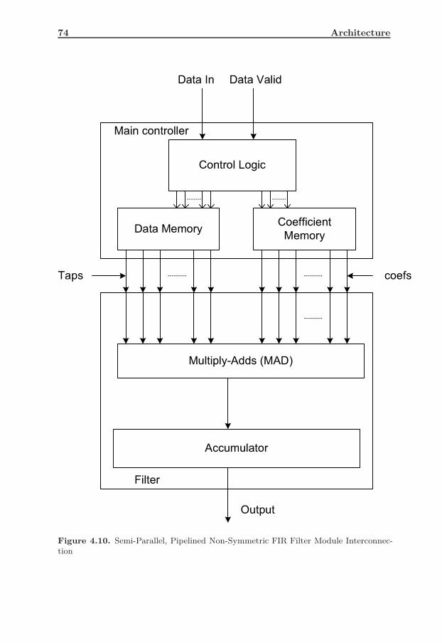
74 Architecture
Figure 4.10. Semi-Parallel, Pipelined Non-Symmetric FIR Filter Module Interconnec-tion
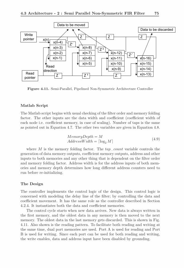
4.3 Architecture - 2 : Semi Parallel Non-Symmetric FIR Filter 75
Figure 4.11. Semi-Parallel, Pipelined Non-Symmetric Architecture Controller
Matlab Script
The Matlab script begins with usual checking of the filter order and memory foldingfactor. The other inputs are the data width and coefficient (coefficient width ofeach node i.e. coefficient memory, in case of scaling). Number of taps is the sameas pointed out in Equation 4.7. The other two variables are given in Equation 4.8.
MemoryDepth =MAddressWidth = ⌈log2M⌉
(4.9)
where M is the memory folding factor. The tap_count variable controls thegeneration of data memory outputs, coefficient memory outputs, address and otherinputs to both memories and any other thing that is dependent on the filter orderand memory folding factor. Address width is for the address inputs of both mem-ories and memory depth determines how long different address counters need torun before re-initializing.
The Design
The controller implements the control logic of the design. This control logic isconcerned with modeling the delay line of the filter; by controlling the data andcoefficient movement. It has the same role as the controller described in Section4.2.4. It instantiates both the data and coefficient memories.
The control cycle starts when new data arrives. New data is always written inthe first memory, and the oldest data in any memory is then moved to the nextmemory. The oldest data in the last memory gets discarded. This is shown in Fig.4.11. Also shown is the reading pattern. To facilitate both reading and writing atthe same time, dual port memories are used. Port A is used for reading and PortB is used for writing. Since each port can be used for both reading and writing,the write enables, data and address input have been disabled by grounding.
76 Architecture
The movement of data within each memory is modeled by pointers. Actual datamovement does not happen. Only when data is to be moved from one memoryto the next, actual data movement takes place. To implement the reading andwriting, the controller uses the following things
• ’1’ read pointer
• ’1’ read address counter
• ’1’ read address enable
• ’1’ write pointer/address counter
• ’1’ coefficient address counter
• ’1’ coefficient address enable
• ’1’ tap enable
The read pointer points to the location from where the memory should be read.The read counter provides the address while read enable enables this read counter.The write pointer, counter and enable also have similar role and so is the role ofcoefficient counter and enable. Tap enable is used to produce output valid.
Since there are no two halves, as was the case in the parallel design, readingpattern is same for all memories. In the reading pattern for this design, the next tooldest data (oldest data is moved to the next memory) is read first and the newlywritten data is read last. This means that each memory is read in the reverseorder. The reason for choosing reverse order instead of the straight order was thatwhen memory was read in straight order, there was always one cycle, where thesame address was accessed, from two different ports, for reading and writing. Thishappened when the new data was being written at a particular address, the datain that location, being the oldest one in that memory, was being read. Although,according to Xilinx, this should result in the old data being read out, which wasalso the desired functionality, but it was found out that this was not happeningfor the last memory. Instead of the old data getting read out, the data beingwritten was being produced on the output port. This was because of the orderin which the two processes for the two ports were being activated. For the allthe memories except the last one, this activation order was such that the correctdata was being read out. However, for the last memory, the process for port Bwas executed before the process for port A. This meant that the new value waswritten first then the old data being read. This meant that the old data was lostand new data was read out.
Based on this observance, it was decided that instead of going into the depthsof the problem, a solution should be reached where such collision is avoided. Thesolution was reading in reverse order. Thus, when writing to a location, say 0,the reading sequence is 1, 2, 3, 4, 5, 0 which is generated by the read counter. Thisindication that reading needs to be started at location 1 is pointed by the readpointer. After this read cycle, the new data is written to the next location i.e.1 and the reading sequence is 2, 3, 4, 5, 0, 1. The write pointer is used to indicate

4.3 Architecture - 2 : Semi Parallel Non-Symmetric FIR Filter 77
this new position where data is to be written. For modeling the data shift acrossmemories, the oldest data in each memory is copied to the next memory. Thisdata resides in the location which will be written with either the new data (incase of first memory) or data from the previous memory. This is done in the sameway as in the parallel architecture. When writing to a new location, the writepointer is immediately incremented pointing to the next location where the nextdata is to be written. This location also contains the oldest data. Thus, this datais available on the output of port B of that memory. The write port (port B) ofthe next memory is permanently connected to the output of port B of the previousmemory. Thus when next data writing takes place, the data from one memory iswritten to the next. Since data writing is synchronous, the new data is writtenimmediately and the old data remains available in that cycle and is written to thenext memory.
In the parallel design, the read pointer is directly connnected to the addressinputs of the read port of all memories. In the same way, the write pointer isconnected to the address inputs of the write port of all memories. The data outputof port B is connected directly to the data input of port B of the next memory.However, in this design, the read pointer is directly connected to only the addressinput of read port of the first memory. The address inputs of all the other memoriesis connected, through a flip-flop, to the address input of the previous memory. Inthe same way, the write pointer is also only connected to the address input of thewrite port of the first memory and for the the other memories, the address inputis connected through a flip-flop to the previous memory’s address input. The datain ports are also connected in the same way as are the write enables. In this way,the pipelined nature is achieved. The data outputs from the memory, thus, arealso pipelined in the form of semi-parallel and so are the tap valids. This is shownin Fig. 4.12.
Since, in a read cycle, it is the oldest data that is read first, the coefficientsalso need to be read in a reverse order. Thus the coefficient counter starts fromthe last address and ends up at location 0. Again, the coefficients are also read inthe same pipelined fashion as described previously.
4.3.5 Data Memory
The data memory serves two purposes
1. Holds Data
2. Models the Delay Line
The same script and file is used as the one in the other design. Refer to Section4.2.5 for details
4.3.6 Coefficient Memory
This module instantiates the individual ROMs which holds the coefficients. It isexactly the same as described in Section 4.2.6. However, there is one difference.

78 Architecture
Figure 4.12. Semi-Parallel, Pipelined Non-Symmetric Architecture Data Out Pattern
4.3 Architecture - 2 : Semi Parallel Non-Symmetric FIR Filter 79
Since this design does not exploit the symmetry of coefficients, the number ofROMs is more than before. Now, for a filter order NO and memory folding factorM the number of ROMs is given by
NumberofROMs = NO/M (4.10)
For further details, refer to Section 4.2.6.
Coefficient Scaling
The same script, scaling.m, is used here as well. Refer to Section 4.2.6 for details.
4.3.7 Main Filter
This module implements the convolution part of the filter. It is named filter.vhdland the script write_fir_filter.m. It performs the multiplication, addition andaccumulation. The general structure of the filter is shown in Fig. 4.9.
The Matlab Script
The Matlab script starts by checking the validity of the inputs. Only one variableis required i.e. tap count and is given in Equation 4.8. This variable controls thegeneration of the module interface, declaration and instantiation of the MAD ele-ments and generating the required signals. This module instantiates the followingtwo modules
1. Multiply-Add
2. Accumulator
The inputs to this script are
• Filter order
• Memory Folding Factor
• Data width
• Coefficient Width (coefficient width for each coefficient ROM in case of scal-ing)
• Multiplier width
• MAD data width
• Final output width

80 Architecture
In the non-scaled version, the output width is 1 more than the MAD outputwidth. The MAD width is simply the sum of data width and coefficient width.For the scaled version, the output width of MAD is determined in a different way.This is because the coefficient width of each node is different.
The output width of the first MAD element is the sum of the data width andthe word length of the input coefficients. Next, the output width of each MAD iseither the sum of its input data width and coefficient widths or the output wordlength of the previous MAD, which ever is larger. The output width is simply thefinal MAD output width plus ’1’.
For the non-scaled version, there is only 1 MAD module, instantiated multipletimes. However, for the scaled version, since each MAD can be of different widthsand code had to be generated that can correctly handle different widths, sepa-rate MAD modules were generated for each node and then properly instantiated.Multiply-Add and Accumulator is explained next.
4.3.8 Multiply-Add
MAD module multiplies the coefficient with the data and adds the output of theprevious MAD stage as indicated in Fig. 4.9. From the figure, it is also evidentthat the second input of the first MAD is 0. It is different from a MAC, becauseit does not add its own output.
The module is named mad.vhdl and the script is write_mad.m. In the scaledversion, however, since each MAD element has different word lengths, each MAD isa different module named madk.vhdl where k has a range from 0 to tapcount− 1.
The Matlab Script
The Matlab script for the non-scaled MAD is simple. It just generates a multiplierand an adder. The multiplier output forms one of the inputs of the adder, thesecond input is the output of the previous MAD element.
However, in the scaled design, the script needs to take into account the outputwidth of the previous stage MAD to properly set word lengths for the adder.The multiplier is again same and the word length is just the addition of the dataand coefficient word lengths. The adder takes the word length of either its ownmultiplier or the previous MAD element, which ever is larger.
The Design
Multiply-Add is a simple module performing two operation in two cycles. First isthe multiplication and second is the addition. The most basic operation in an FIRis convolution. It involves multiplication and addition. Either this could be inthe form of multiply-accumulate, as is the case when only one multiplier/adder isused, or multiply-add, as is in the case of direct form structures as shown in Figs.2.4 and 2.5. However, for time-multiplexed structures, either MACs are needed oran Accumulator is needed after all these MAD-operations.
Each of the two operations takes one cycle as shown in Fig. 4.13. One of theinputs of the multiplier is the incoming tap from the data memory while other

4.3 Architecture - 2 : Semi Parallel Non-Symmetric FIR Filter 81
Figure 4.13. Multiply-Add (MAD)
is the filter coefficient from the coefficient memory. The output of this multiplierforms one input of the adder and the other input is the previous MAD’s output.For the first element, no adder is needed. So, the second input of the adder is 0.
4.3.9 Accumulator (ACC)
The accumulator accumulates the output of the final MAD element. The needfor accumulator arose because of the time-multiplexed nature of input where theintermediate outputs of MAD need to be accumulated to produce the final result.As explained before, either a MAC based architecture is needed, as was done in theparallel design, or an accumulator is needed for multiply-add based design. Theaccumulator here is named acc.vhdl and the Matlab script is named write_acc.m.
For the accumulator to start and stop the accumulation at the right time, acounter is used that counts for clock cycles equal to the memory folding factor.The script is used to calculate the total number of cycles for which accumulationhas to be performed and thus the width of the counter. Both these variables aregiven in Equation 4.11.
CycleCount =MCounterWidth = ⌈log2M⌉ (4.11)
where M is the memory folding factor. When the accumulation of one filteroutput is finished, an output valid is generated which acts as the output valid ofthe whole filter.
4.3.10 Functional Simulation
After the completion of design, the next step was functional simulation. Theprocedure was same as highlighted in Section 4.2.11. The test bench, simulationscript and behavioral model were all generated using Matlab script. They werethe same as used in the parallel design. For details, refer to Section 4.2.11.
82 Architecture
4.3.11 Synthesis and Implementation
After functional simulation, the next step was synthesis and implementation onthe targeet FPGA. The same steps were followed as highlighted for the paralleldesign. Refer to Section 4.1.4 for details.
4.3.12 Post PAR Simulation
Post PAR simulation is the second-last step in the design cycle. It involves testingthe placed and routed design. Successful completion of this step ensures that theimplemented is working correctly. This step was again the same as in paralleldesign. Refer to Sections 4.2.13 and 4.1.5 for complete details
4.3.13 Power Estimation
Power estimation was also done in the same way using Xilinx application calledxpower. Refer to Section 4.1.6 for complete details.
4.3.14 Xilinx FIR Compiler
Xilinx FIR Compiler was again used to compare frequency, resource utilizationand power dissipation. All of the details are available in Section 4.2.15. Amongthe inputs mentioned in Section 4.2.15, only the coefficient structure is changedwith respect to the parallel design. Since symmetry was not to be exploited, thecoefficient structure was selected as Non-Symmetric. All other inputs were keptthe same. For more details, kindly refer to Section 4.2.15.
Chapter 5
Results
This chapter deals with all the results of the implemented designs, their comparisonwith each other and with that of the Xilinx FIR compiler. There are ’3’ maindimensions to the results
• Resource utilization of the FPGA
– Slice Count (SC)
– Block Random Access Memory (BRAM) Count (BC)
– DSP48E Slice Count (DSPC)
• Clock Frequency (CF)
• Power Dissipation (PD)
As mentioned in Section 4.1.6, power dissipation requires a VCD file to obtainfrequency and activity rates of internal signals. This file is created during postPAR simulation. This simulation was run at a clock frequency of 100MHz for allthe architectures as well as the FIR core generated by Xilinx core generator.
The comparison will be made between the following
• Scaled and Non-Scaled - All Filter orders and memory folding factors
– Parallel vs Semi-Parallel (Pipelined) - Slice Count
– Parallel vs Semi-Parallel (Pipelined) - BRAM Count
– Parallel vs Semi-Parallel (Pipelined) - DSP48E Slice Count
– Parallel vs Semi-Parallel (Pipelined) - Clock Frequency
– Parallel vs Semi-Parallel (Pipelined) - Power Dissipation
• Scaled and Non-Scaled
– Parallel (Order N) vs Parallel (Order N + 1) - Slice Count
– Parallel (Order N) vs Parallel (Order N + 1) - BRAM Count
83
84 Results
– Parallel (Order N) vs Parallel (Order N + 1) - DSP48E Slice Count
– Parallel (Order N) vs Parallel (Order N + 1) - Clock Frequency
– Parallel (Order N) vs Parallel (Order N + 1) - Power Dissipation
• Scaled and Non-Scaled
– Semi-Parallel (Order N) vs Semi-Parallel (Order N + 1) - Slice Count
– Semi-Parallel (Order N) vs Semi-Parallel (Order N+1) - BRAM Count
– Semi-Parallel (Order N) vs Semi-Parallel (Order N+1) - DSP48E SliceCount
– Semi-Parallel (OrderN) vs Semi-Parallel (OrderN+1) - Clock Frequency
– Semi-Parallel (OrderN) vs Semi-Parallel (OrderN+1) - Power Dissipation
• Parallel and Semi-Parallel (Pipelined) - All filter orders and memory foldingfactors
– Scaled vs Non-Scaled - Slice Count
– Scaled vs Non-Scaled - BRAM Count
– Scaled vs Non-Scaled - DSP48E Slice Count
– Scaled vs Non-Scaled - Clock Frequency
– Scaled vs Non-Scaled - Power Dissipation
• Parallel, Non-Scaled, same Filter Order - Effect of change in memory foldingfactor
• Parallel, Scaled, same Filter Order - Effect of change in memory foldingfactor
• Semi-Parallel (Pipelined), Non-Scaled, same Filter Order - Effect of changein memory folding factor
• Semi-Parallel (Pipelined), Scaled, same Filter Order - Effect of change inmemory folding factor
• Parallel, Non-Scaled, same Filter Order - Effect of change in data width
• Parallel, Scaled, same Filter Order - Effect of change in data width
• Semi-Parallel, Non-Scaled, same Filter Order - Effect of change in data width
• Semi-Parallel, Scaled, same Filter Order - Effect of change in data width
• Implemented Design vs Xilinx FIR Compiler - Parallel (Scaled and Non-Scaled), Semi-Parallel (Scaled and Non-Scaled) - All filter orders and memoryfolding factors
5.1 Xilinx Resource Facts 85
The resource utilization (Slice Count, BRAM Count, DSP48E Slice Count)and Clock Frequency were obtained using Xilinx ISE Software. All numbers areobtained after complete place and route. The Power Dissipation is provided byrunning xpower utility of Xilinx on the post PAR simulation data. Coefficientword length is always 18-bits while data word length is either 18-bits or 24-bits.Each architecture has ’2’ version, scaled and non-scaled. Two FPGAs are used.LX20T and LX50T. LX50T is used for filter order 127 and higher, because thenumber of BRAMs available in 20T was not enough to fit in the design, especiallyfor 24-bit word lengths. Details about these two FPGAs are available in 3.10.1
The synthesis and implementation was performed using standard settings.Data memories were forced to be implemented as BRAMs and coefficient memo-ries as Distributed ROMs. Inferrence DSP48E slice was left at Auto. This meantthat any multiplications, MACs or MADs will be implemented as DSP48E slicewhile normal adders will be implemented in the FPGA fabric.
Each of the results will be explained next. Along with the explanation, ac-tual numerical values, tables and/or graphs will also be presented as appropriate.However, before presenting the comparisons, few facts about Xilinx resources arepresented as well as some of Altera’s results that were revealed early on.
5.1 Xilinx Resource Facts
The Xilinx resources, BRAM and DSP48E elements, require a specific way ofwriting code. If not followed, results acheived would not be optimum
• DSP Elements
– Supports ’Add’ operation in DSP but inference has to be forced
– Supports ’MAC’, infers it automatically
– Doesn’t support asynchronous reset, so all registers with asynchronousreset were implemented in logic
– Supports synchronous reset and all registers were absorbed in the DSPblock.
• Block RAMs
– Requires a shared variable (shared variable RAM: ram_type;) to inferRAM.
– For dual port memories, two separate processes are needed. Each pro-cess is trigerred on a rising clock edge with synchronous reset.
– Reading and writing the same address from different ports producesuncertain behaviour. This is in contrast to what Xilinx claims, whereold data is always read out.

86 Results
5.2 Altera Resource Facts
• DSP Elements
– Doesn’t support ’Add’ operation in DSP as the Adder block in theDSP block cannot be used independently of the multiplier. Adders arealways implemented in logic slices.
– With Synchronous Reset, some part of logic is implemented in LUTswhile some in DSP although no explicit MAC was inferred
– With Asynchronous Reset, everything was implemented in DSP andMAC operation was also recognized.
• Memory
– It requires specifically to write code so that when same memory locationis addressed from different ports, one for read and one for write, olddata is read.
– It required the address ports to be of type natural instead of std_logic_vector
– Although the memory model for altera was coded according to theguidelines [27], the data was not being written to the memory.
Due to this problem, mapping of FIR filters on Altera’s FPGA was droppedand all focus put on Xilinx.
5.3 Comparison-1, Non-Scaled Filter, Parallel vs
Semi-Parallel: Slice Count
Here the two architectures implemented, with no scaling, will be compared withrespecte to the Slice Count. The design uses the slices to implement control logicand distributed ROMs. Table 5.1 shows the result in tabular form while Fig. 5.1represents the graph for 18-bit data word length.
Here, O is the filter order, FF is the memory folding factor, NO is the new in-creased order for even-ordered filters implemented using the pipelined architectureand 50T indicates that LX50T FPGA is used.
Figure 5.1 shows it in grapical format. For small filters, the difference is notmuch because the number of adders in both architectures is similar. However,as the filter order increases, the disparity increases and the pipelined architectureshows a major reduction. Furthermore, increasing the filter order by ’1’ does notincur a very high penalty.
5.4 Comparison-2, Non-Scaled, Parallel vs Semi-Parallel: BRAM Count
Block RAMs (BRAMs) are used to implement the data memory. Here the com-parison will be based on 18-K BRAM. As mentioned in 3.10.1, BRAMs can either

5.5 Comparison-3, Non-Scaled, Parallel vs Semi-Parallel: DSP48E SliceCount 87
Parallel Semi-Parallel NoteO = 15 , FF = 4 45 67O = 16 , FF = 4 73 61 NO = 19O = 19 , FF = 10 35 58O = 20 , FF = 10 61 59 NO = 29O = 23 , FF = 4 80 79O = 24 , FF = 4 74 75 NO = 27O = 59 , FF = 10 95 70O = 60 , FF = 10 104 77 NO = 69O = 99 , FF = 10 130 99O = 100, FF = 10 141 101 NO = 109O = 108, FF = 6 216 159 NO = 113O = 127, FF = 4 315 234 50TO = 128, FF = 4 341 207 NO = 131, 50T
Table 5.1. Slice Comparison
be used as 1 36K BRAM or 2 18K BRAMs.
For odd-order filters, there was no difference between the two architecturesfor same filter order and memory folding factor. Both used the same amount ofBRAMs. However, since in the semi-parallel (pipelined) design, the even orderfilters were changed to odd order filters to avoid the one extra central tap, BRAMusage increased. This increase, for 18-bit data word length, was always 1 18-KBRAM while for 24-bit data word length, it was 2. The difference between 18-bitand 24-bit will be explained later.
5.5 Comparison-3, Non-Scaled, Parallel vs Semi-Parallel: DSP48E Slice Count
DSP48E Slices are used to implement the MACs in the parallel architecture andMADs in the semi-parallel(pipelined) architecture. Table 5.2 shows DSP48E sliceutilization against different filter orders and memory folding factors for the twoarchitectures with 18-bit data word length.
Here, O is the filter order, FF is the memory folding factor, NO is the newincreased order for even-ordered filters implemented using the pipelined architec-ture and 50T indicates that LX50T FPGA is used. For other filters, LX20T isused.
As expected, the number of DSP48E elements used by the pipelined designis twice as it does not utilize the symmetery of coefficients. Also, a penalty of1 DSP48E element is incurred when filter order is increased by 1 to make it aneven order filter. This is because, in the parallel architecture, the extra tap needs1 more MAC unit. In the other architecture, this increase is due to the extramemory required for the increased filter order. Figure 5.2 plots these results.

88 Results
50
100
150
200
250
300
350
Filter Order, Memory Folding Factor
Logi
c S
lice
Cou
nt
15,4 16,4 19,10 20,10 23,4 24,4 59,10 60,10 99,10 100,10 108,6 127,4 128,4
ParallelSemi−Parallel
Figure 5.1. Slice Comparison
5.6 Comparison-4, Non-Scaled, Parallel vs Semi-Parallel: Clock Frequency
Clock frequency indicates how fast can the filter be operated. It is the inverse ofthe critical path timing. Table 5.3 shows clock frequencies achieved for differentcases.
The graph is given in 5.3. It is quite clear from these results that the pipelinedarchitecture achieves higher frequency. This is due to the pipelined nature of thearchitecture. Furthermore, increasing the filter order by 1 actually, in most cases,increases the frequency.
5.7 Comparison-5, Non-Scaled, Parallel vs Semi-
Parallel: Power Dissipation
The power dissipation was calculated using Xilinx application called xpower. Thisapplication uses simulation data generated by the post PAR simulation. Resultsare described in Table 5.4 and Fig. 5.4.
It is evident that the pipelined architecture consumes more power as comparedto the parallel architecture. More DSP48E elements usage contributes directly tothis higher power dissipation. Also, extra pipeline registers between the memoriesalso contribute.
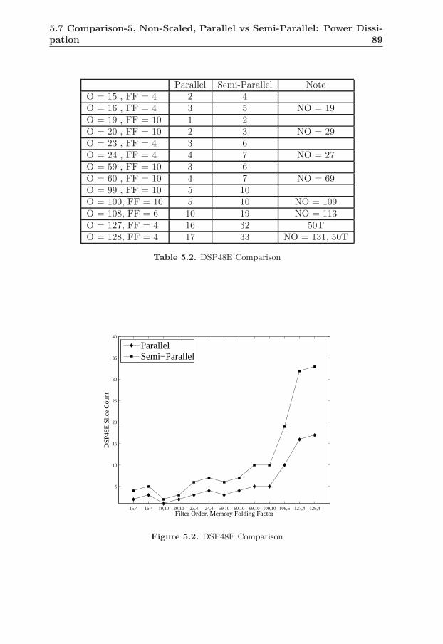
5.7 Comparison-5, Non-Scaled, Parallel vs Semi-Parallel: Power Dissi-pation 89
Parallel Semi-Parallel NoteO = 15 , FF = 4 2 4O = 16 , FF = 4 3 5 NO = 19O = 19 , FF = 10 1 2O = 20 , FF = 10 2 3 NO = 29O = 23 , FF = 4 3 6O = 24 , FF = 4 4 7 NO = 27O = 59 , FF = 10 3 6O = 60 , FF = 10 4 7 NO = 69O = 99 , FF = 10 5 10O = 100, FF = 10 5 10 NO = 109O = 108, FF = 6 10 19 NO = 113O = 127, FF = 4 16 32 50TO = 128, FF = 4 17 33 NO = 131, 50T
Table 5.2. DSP48E Comparison
5
10
15
20
25
30
35
40
Filter Order, Memory Folding Factor
DS
P48
E S
lice
Cou
nt
15,4 16,4 19,10 20,10 23,4 24,4 59,10 60,10 99,10 100,10 108,6 127,4 128,4
ParallelSemi−Parallel
Figure 5.2. DSP48E Comparison
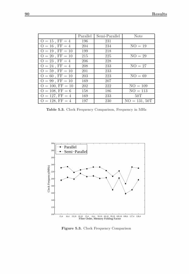
90 Results
Parallel Semi-Parallel NoteO = 15 , FF = 4 196 231O = 16 , FF = 4 204 234 NO = 19O = 19 , FF = 10 199 218O = 20 , FF = 10 215 225 NO = 29O = 23 , FF = 4 206 228O = 24 , FF = 4 208 233 NO = 27O = 59 , FF = 10 201 233O = 60 , FF = 10 203 223 NO = 69O = 99 , FF = 10 169 207O = 100, FF = 10 202 222 NO = 109O = 108, FF = 6 158 186 NO = 113O = 127, FF = 4 169 233 50TO = 128, FF = 4 197 230 NO = 131, 50T
Table 5.3. Clock Frequency Comparison, Frequency in MHz
100
120
140
160
180
200
220
240
260
280
300
Filter Order, Memory Folding Factor
Clo
ck F
requ
ency
(MH
z)
15,4 16,4 19,10 20,10 23,4 24,4 59,10 60,10 99,10 100,10 108,6 127,4 128,4
ParallelSemi−Parallel
Figure 5.3. Clock Frequency Comparison
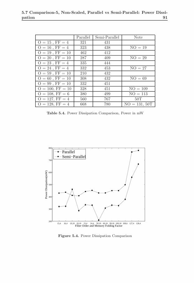
5.7 Comparison-5, Non-Scaled, Parallel vs Semi-Parallel: Power Dissi-pation 91
Parallel Semi-Parallel NoteO = 15 , FF = 4 321 431O = 16 , FF = 4 323 438 NO = 19O = 19 , FF = 10 462 412O = 20 , FF = 10 287 409 NO = 29O = 23 , FF = 4 335 444O = 24 , FF = 4 332 453 NO = 27O = 59 , FF = 10 210 432O = 60 , FF = 10 308 432 NO = 69O = 99 , FF = 10 332 451O = 100, FF = 10 328 451 NO = 109O = 108, FF = 6 380 499 NO = 113O = 127, FF = 4 560 767 50TO = 128, FF = 4 668 780 NO = 131, 50T
Table 5.4. Power Dissipation Comparison, Power in mW
200
300
400
500
600
700
800
Filter Order and Memory Folding Factor
Pow
er D
issi
patio
n(m
W)
15,4 16,4 19,10 20,10 23,4 24,4 59,10 60,10 99,10 100,10 108,6 127,4 128,4
ParallelSemi−Parallel
Figure 5.4. Power Dissipation Comparison
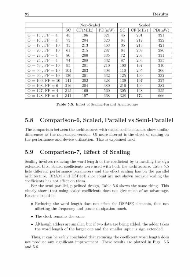
92 Results
Non-Scaled ScaledSC CF(MHz) PD(mW) SC CF(MHz) PD(mW)
O = 15 , FF = 4 45 196 321 45 201 321O = 16 , FF = 4 73 204 323 84 212 322O = 19 , FF = 10 35 213 463 35 213 421O = 20 , FF = 10 61 215 287 64 209 286O = 23 , FF = 4 80 206 335 72 203 331O = 24 , FF = 4 74 208 332 87 203 335O = 59 , FF = 10 95 201 210 100 197 310O = 60 , FF = 10 104 203 308 110 205 306O = 99 , FF = 10 130 201 332 125 199 332O = 100, FF = 10 141 202 328 139 197 327O = 108, FF = 6 216 204 380 216 199 382O = 127, FF = 4 315 169 560 305 168 555O = 128, FF = 4 341 197 668 328 172 666
Table 5.5. Effect of Scaling-Parallel Architecture
5.8 Comparison-6, Scaled, Parallel vs Semi-Parallel
The comparison between the architectures with scaled coefficients also show similardifferences as the non-scaled version. Of more interest is the effect of scaling onthe performance and device utilization. This is explained next.
5.9 Comparison-7, Effect of Scaling
Scaling involves reducing the word length of the coefficient by truncating the signextended bits. Scaled coefficients were used with both the architecture. Table 5.5lists different performance parameters and the effect scaling has on the parallelarchitecture. BRAM and DSP48E slice count are not shown becasue scaling thecoefficients has not effect on them.
For the semi-parallel, pipelined design, Table 5.6 shows the same thing. Thisclearly shows that using scaled coefficients does not give much of an advantage.Reasons could be
• Reducing the word length does not effect the DSP48E elements, thus notaffecting the frequency and power dissipation much.
• The clock remains the same.
• Although adders are smaller, but if two data are being added, the adder takesthe word length of the larger one and the smaller input is sign extended.
Thus, it can be safely concluded that reducing the coefficient word length doesnot produce any significant improvement. These results are plotted in Figs. 5.5and 5.6.

5.9 Comparison-7, Effect of Scaling 93
Non-Scaled ScaledSC CF(MHz) PD(mW) SC CF(MHz) PD(mW)
O = 15 , FF = 4 67 231 431 67 231 432O = 16 , FF = 4 61 234 438 61 234 438O = 19 , FF = 10 58 231 412 58 232 411O = 20 , FF = 10 59 225 409 54 231 365O = 23 , FF = 4 79 228 444 79 228 444O = 24 , FF = 4 75 233 453 74 234 414O = 59 , FF = 10 70 233 432 70 234 432O = 60 , FF = 10 77 223 432 72 223 385O = 99 , FF = 10 99 232 451 99 232 451O = 100, FF = 10 101 222 451 102 222 406O = 108, FF = 6 159 232 499 154 232 462O = 127, FF = 4 234 233 767 233 233 767O = 128, FF = 4 207 230 780 207 232 737
Table 5.6. Effect of Scaling-Pipelined Architecture
100
200
300
400
Filter Order, Memory Folding Factor
Slic
e C
ount
15,4 16,4 19,10 20,10 23,4 24,4 59,10 60,10 99,10 100,10 108,6 127,4 128,4
Non−ScaledScaled
100
200
300
400
Filter Order, Memory Folding FactorClo
ck F
requ
ency
(MH
z)
15,4 16,4 19,10 20,10 23,4 24,4 59,10 60,10 99,10 100,10 108,6 127,4 128,4
Non−ScaledScaled
200
300
400
500
600
700
Filter Order, Memory Folding FactorPow
er D
issi
patio
n(m
W)
15,4 16,4 19,10 20,10 23,4 24,4 59,10 60,10 99,10 100,10 108,6 127,4 128,4
Non−ScaledScaled
Figure 5.5. Effect of Scaling on Parallel Architecture

94 Results
50
100
150
200
250
300
Filter Order, Memory Folding Factor
Slic
e C
ount
15,4 16,4 19,10 20,10 23,4 24,4 59,10 60,10 99,10 100,10 108,6 127,4 128,4
Non−ScaledScaled
150
200
250
300
350
400
Filter Order, Memory Folding FactorClo
ck F
requ
ency
(MH
z)
15,4 16,4 19,10 20,10 23,4 24,4 59,10 60,10 99,10 100,10 108,6 127,4 128,4
Non−ScaledScaled
400
600
800
1000
Filter Order, Memory Folding FactorPow
er D
issi
patio
n(m
W)
15,4 16,4 19,10 20,10 23,4 24,4 59,10 60,10 99,10 100,10 108,6 127,4 128,4
Non−ScaledScaled
Figure 5.6. Effect of Scaling on Semi-Parallel, Pipelined Architecture
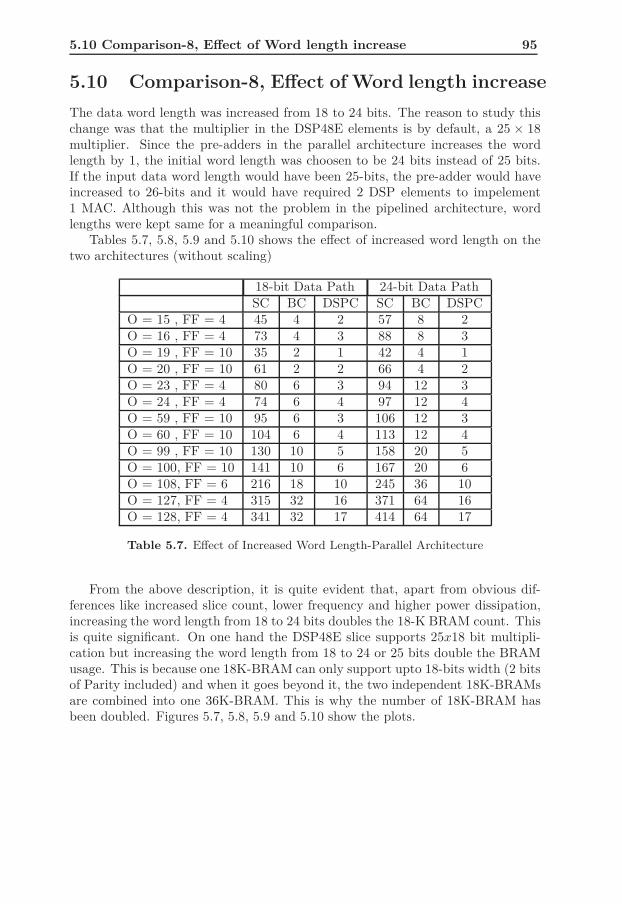
5.10 Comparison-8, Effect of Word length increase 95
5.10 Comparison-8, Effect of Word length increase
The data word length was increased from 18 to 24 bits. The reason to study thischange was that the multiplier in the DSP48E elements is by default, a 25 × 18multiplier. Since the pre-adders in the parallel architecture increases the wordlength by 1, the initial word length was choosen to be 24 bits instead of 25 bits.If the input data word length would have been 25-bits, the pre-adder would haveincreased to 26-bits and it would have required 2 DSP elements to impelement1 MAC. Although this was not the problem in the pipelined architecture, wordlengths were kept same for a meaningful comparison.
Tables 5.7, 5.8, 5.9 and 5.10 shows the effect of increased word length on thetwo architectures (without scaling)
18-bit Data Path 24-bit Data PathSC BC DSPC SC BC DSPC
O = 15 , FF = 4 45 4 2 57 8 2O = 16 , FF = 4 73 4 3 88 8 3O = 19 , FF = 10 35 2 1 42 4 1O = 20 , FF = 10 61 2 2 66 4 2O = 23 , FF = 4 80 6 3 94 12 3O = 24 , FF = 4 74 6 4 97 12 4O = 59 , FF = 10 95 6 3 106 12 3O = 60 , FF = 10 104 6 4 113 12 4O = 99 , FF = 10 130 10 5 158 20 5O = 100, FF = 10 141 10 6 167 20 6O = 108, FF = 6 216 18 10 245 36 10O = 127, FF = 4 315 32 16 371 64 16O = 128, FF = 4 341 32 17 414 64 17
Table 5.7. Effect of Increased Word Length-Parallel Architecture
From the above description, it is quite evident that, apart from obvious dif-ferences like increased slice count, lower frequency and higher power dissipation,increasing the word length from 18 to 24 bits doubles the 18-K BRAM count. Thisis quite significant. On one hand the DSP48E slice supports 25x18 bit multipli-cation but increasing the word length from 18 to 24 or 25 bits double the BRAMusage. This is because one 18K-BRAM can only support upto 18-bits width (2 bitsof Parity included) and when it goes beyond it, the two independent 18K-BRAMsare combined into one 36K-BRAM. This is why the number of 18K-BRAM hasbeen doubled. Figures 5.7, 5.8, 5.9 and 5.10 show the plots.

96 Results
18-bit Data Path 24-bit Data PathCF(MHz) PD(mW) CF(MHz) PD(mW)
O = 15 , FF = 4 196 321 197 340O = 16 , FF = 4 204 323 199 341O = 19 , FF = 10 213 463 203 454O = 20 , FF = 10 215 287 201 296O = 23 , FF = 4 206 335 193 357O = 24 , FF = 4 208 332 196 357O = 59 , FF = 10 201 210 199 328O = 60 , FF = 10 203 308 201 326O = 99 , FF = 10 201 332 169 391O = 100, FF = 10 202 328 197 358O = 108, FF = 6 204 380 160 440O = 127, FF = 4 169 560 163 748O = 128, FF = 4 197 668 164 744
Table 5.8. Effect of Increased Word Length-Parallel Architecture
18-bit Data Path 24-bit Data PathSC BC DSPC SC BC DSPC
O = 15 , FF = 4 67 4 4 51 8 4O = 16 , FF = 4 61 5 5 57 10 5O = 19 , FF = 10 58 2 2 45 4 2O = 20 , FF = 10 59 3 3 49 6 3O = 23 , FF = 4 79 6 6 70 12 6O = 24 , FF = 4 75 7 7 76 14 7O = 59 , FF = 10 70 6 6 78 12 6O = 60 , FF = 10 77 7 7 76 14 7O = 99 , FF = 10 99 10 10 99 20 10O = 100, FF = 10 101 11 11 103 22 11O = 108, FF = 6 159 19 19 158 38 19O = 127, FF = 4 234 32 32 235 64 32O = 128, FF = 4 207 33 33 189 66 33
Table 5.9. Effect of Increased Word Length-Pipelined Architecture
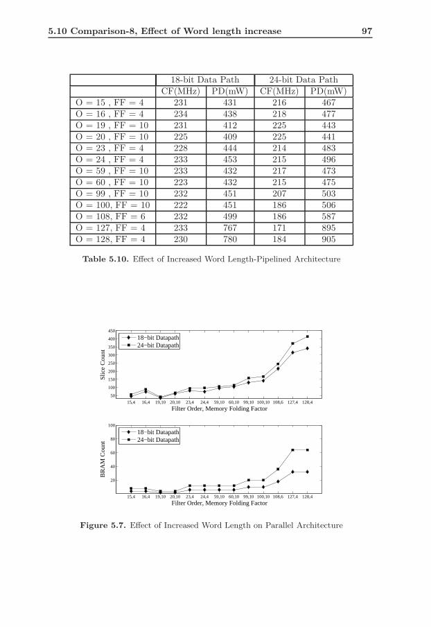
5.10 Comparison-8, Effect of Word length increase 97
18-bit Data Path 24-bit Data PathCF(MHz) PD(mW) CF(MHz) PD(mW)
O = 15 , FF = 4 231 431 216 467O = 16 , FF = 4 234 438 218 477O = 19 , FF = 10 231 412 225 443O = 20 , FF = 10 225 409 225 441O = 23 , FF = 4 228 444 214 483O = 24 , FF = 4 233 453 215 496O = 59 , FF = 10 233 432 217 473O = 60 , FF = 10 223 432 215 475O = 99 , FF = 10 232 451 207 503O = 100, FF = 10 222 451 186 506O = 108, FF = 6 232 499 186 587O = 127, FF = 4 233 767 171 895O = 128, FF = 4 230 780 184 905
Table 5.10. Effect of Increased Word Length-Pipelined Architecture
50
100
150
200
250
300
350
400
450
Filter Order, Memory Folding Factor
Slic
e C
ount
15,4 16,4 19,10 20,10 23,4 24,4 59,10 60,10 99,10 100,10 108,6 127,4 128,4
18−bit Datapath24−bit Datapath
20
40
60
80
100
Filter Order, Memory Folding Factor
BR
AM
Cou
nt
15,4 16,4 19,10 20,10 23,4 24,4 59,10 60,10 99,10 100,10 108,6 127,4 128,4
18−bit Datapath24−bit Datapath
Figure 5.7. Effect of Increased Word Length on Parallel Architecture
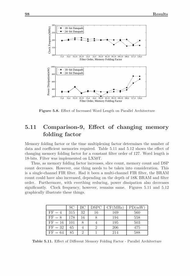
98 Results
100
150
200
250
300
Filter Order, Memory Folding Factor
Clo
ck F
requ
ency
(MH
z)
15,4 16,4 19,10 20,10 23,4 24,4 59,10 60,10 99,10 100,10 108,6 127,4 128,4
18−bit Datapath24−bit Datapath
200
400
600
800
1000
Filter Order, Memory Folding Factor
Pow
er D
issi
patio
n(m
W)
15,4 16,4 19,10 20,10 23,4 24,4 59,10 60,10 99,10 100,10 108,6 127,4 128,4
18−bit Datapath24−bit Datapath
Figure 5.8. Effect of Increased Word Length on Parallel Architecture
5.11 Comparison-9, Effect of changing memoryfolding factor
Memory folding factor or the time multiplexing factor determines the number ofdata and coefficient memories required. Table 5.11 and 5.12 shows the effect ofchanging memory folding factor for a constant filter order of 127. Word length is18-bits. Filter was implemented on LX50T.
Thus, as memory folding factor increases, slice count, memory count and DSPcount decreases. However, one thing needs to be taken into consideration. Thisis a single-channel FIR filter. Had it been a multi-channel FIR filter, the BRAMcount could have also increased, depending on the depth of 18K BRAM and filterorder. Furthermore, with everthing reducing, power dissipation also decreasessignificantly. Clock frequency, however, remains same. Figures 5.11 and 5.12graphically illustrate these things.
SC BC DSPC CF(MHz) PD(mW)FF = 4 315 32 16 169 560FF = 8 178 16 8 194 558FF = 16 101 8 4 195 503FF = 32 65 4 2 206 475FF = 64 85 2 1 214 588
Table 5.11. Effect of Different Memory Folding Factor - Parallel Architecture

5.11 Comparison-9, Effect of changing memory folding factor 99
SC BC DSPC CF(MHz) PD(mW)FF = 4 234 32 32 233 767FF = 8 136 16 16 233 674FF = 16 87 8 8 230 624FF = 32 79 4 4 233 596FF = 64 51 2 2 233 576
Table 5.12. Effect of Different Memory Folding Factor - Pipelined Architecture
50
100
150
200
250
300
350
400
450
Filter Order, Memory Folding Factor
Slic
e C
ount
15,4 16,4 19,10 20,10 23,4 24,4 59,10 60,10 99,10 100,10 108,6 127,4 128,4
18−bit Datapath24−bit Datapath
20
40
60
80
100
Filter Order, Memory Folding Factor
BR
AM
Cou
nt
15,4 16,4 19,10 20,10 23,4 24,4 59,10 60,10 99,10 100,10 108,6 127,4 128,4
18−bit Datapath24−bit Datapath
Figure 5.9. Effect of Increased Word Length on Semi-Parallel, Pipelined Architecture
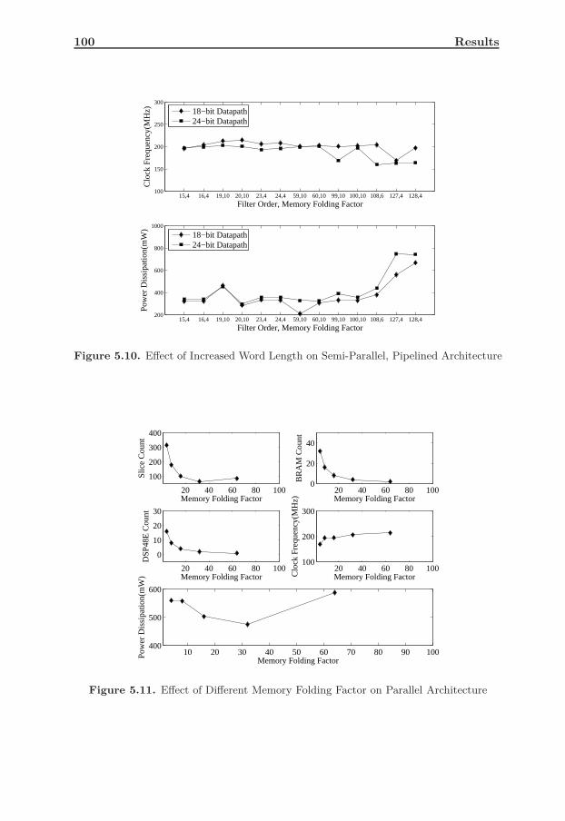
100 Results
100
150
200
250
300
Filter Order, Memory Folding Factor
Clo
ck F
requ
ency
(MH
z)
15,4 16,4 19,10 20,10 23,4 24,4 59,10 60,10 99,10 100,10 108,6 127,4 128,4
18−bit Datapath24−bit Datapath
200
400
600
800
1000
Filter Order, Memory Folding Factor
Pow
er D
issi
patio
n(m
W)
15,4 16,4 19,10 20,10 23,4 24,4 59,10 60,10 99,10 100,10 108,6 127,4 128,4
18−bit Datapath24−bit Datapath
Figure 5.10. Effect of Increased Word Length on Semi-Parallel, Pipelined Architecture
20 40 60 80 100
100
200
300
400
Memory Folding Factor
Slic
e C
ount
20 40 60 80 1000
20
40
Memory Folding Factor
BR
AM
Cou
nt
20 40 60 80 100
0
10
20
30
Memory Folding Factor
DS
P48
E C
ount
20 40 60 80 100100
200
300
Memory Folding FactorClo
ck F
requ
ency
(MH
z)
10 20 30 40 50 60 70 80 90 100400
500
600
Memory Folding Factor
Pow
er D
issi
patio
n(m
W)
Figure 5.11. Effect of Different Memory Folding Factor on Parallel Architecture

5.11 Comparison-9, Effect of changing memory folding factor 101
20 40 60 80 100
100
200
300
Memory Folding Factor
Slic
e C
ount
20 40 60 80 1000
20
40
Memory Folding Factor
BR
AM
Cou
nt
20 40 60 80 1000
20
40
Memory Folding Factor
DS
P48
E C
ount
20 40 60 80 100100
200
300
Memory Folding FactorClo
ck F
requ
ency
(MH
z)
10 20 30 40 50 60 70 80 90 100500
600
700
800
Memory Folding Factor
Pow
er D
issi
patio
n(m
W)
Figure 5.12. Effect of Different Memory Folding Factor on Semi-Parallel, PipelinedArchitecture

102 Results
5.12 Comparison-10 Implemented Design vs Xil-
inx FIR Compiler
In this section, the performance and resource utilization of the implemented designis compared with that of Xilinx FIR Core genereated using Core Generator. TheFIR core was generated for all cases i.e. Symmetric and Non-Symmetric, 18 and 24bits data path so that a complete performance is possible. In the next sub-sections,each case will be examined.
5.12.1 Parallel Architecture (Symmetric), 18-bit Data Path
Tables 5.13 and 5.14 and Figs. 5.13 and 5.14 compare the Parallel Architecturewith Xilinx FIR Core using coefficient symmetry for 18-bit data path
5.12.2 Parallel Architecture (Symmetric), 24-bit Data Path
Tables 5.15 and 5.16 and Figs. 5.15 and 5.16 compare the Parallel Architecturewith Xilinx FIR Core using coefficient symmetry for 24-bit data path
5.12.3 Semi-Parallel Architecture (Non-Symmetric), 18-bitData Path
Tables 5.17 and 5.18 and Figs. 5.17 and 5.18 compare the Semi-Parallel Architec-ture with Xilinx FIR Core non using coefficient symmetry for 18-bit data path
5.12.4 Semi-Parallel Architecture (Non-Symmetric), 24-bitData Path
Tables 5.19 and 5.20 and Fig. 5.19 and 5.20 compare the Semi-Parallel Architec-ture with Xilinx FIR Core not using coefficient symmetry for 24-bit data path

5.12 Comparison-10 Implemented Design vs Xilinx FIR Compiler 103
Parallel Architecture Symmetric Xilinx FIR CoreSC BC DSPC SC BC DSPC
O = 15 , FF = 4 45 4 2 102 2 3O = 16 , FF = 4 73 4 3 130 3 4O = 19 , FF = 10 35 2 1 80 1 1O = 20 , FF = 10 61 2 2 100 2 3O = 23 , FF = 4 80 6 3 132 3 4O = 24 , FF = 4 74 6 4 160 4 5O = 59 , FF = 10 95 6 3 140 3 4O = 60 , FF = 10 104 6 4 171 4 5O = 99 , FF = 10 130 10 5 218 5 6O = 100, FF = 10 141 10 6 246 6 7O = 108, FF = 6 216 18 10 376 10 11O = 127, FF = 4 315 32 16 553 16 17O = 128, FF = 4 341 32 17 754 17 18
Table 5.13. Parallel Architecture vs Symmmetric FIR Core - 18 bit data path
Parallel Architecture Symmetric Xilinx FIR CoreCF(MHz) PD(mW) CF(MHz) PD(mW)
O = 15 , FF = 4 196 321 527 606O = 16 , FF = 4 204 323 490 619O = 19 , FF = 10 213 463 554 315O = 20 , FF = 10 215 287 545 319O = 23 , FF = 4 206 335 501 636O = 24 , FF = 4 208 332 519 650O = 59 , FF = 10 201 210 478 344O = 60 , FF = 10 203 308 495 347O = 99 , FF = 10 201 332 510 365O = 100, FF = 10 202 328 485 370O = 108, FF = 6 204 380 474 559O = 127, FF = 4 169 560 461 1133O = 128, FF = 4 197 668 351 1224
Table 5.14. Parallel Architecture vs Symmmetric FIR Core - 18 bit data path
104 Results
200
400
600
800
Filter Order, Memory Folding Factor
Slic
e C
ount
15,4 16,4 19,10 20,10 23,4 24,4 59,10 60,10 99,10 100,10 108,6 127,4 128,4
Implemented DesignFIR Core
0
10
20
30
40
50
Filter Order, Memory Folding Factor
BR
AM
Cou
nt
15,4 16,4 19,10 20,10 23,4 24,4 59,10 60,10 99,10 100,10 108,6 127,4 128,4
Implemented DesignFIR Core
0
10
20
30
Filter Order, Memory Folding Factor
DS
P48
E C
ount
15,4 16,4 19,10 20,10 23,4 24,4 59,10 60,10 99,10 100,10 108,6 127,4 128,4
Implemented DesignFIR Core
Figure 5.13. Parallel Architecture vs Symmmetric FIR Core - 18 bit data path
200
400
600
800
1000
Filter Order, Memory Folding Factor
Clo
ck F
requ
ency
(MH
z)
15,4 16,4 19,10 20,10 23,4 24,4 59,10 60,10 99,10 100,10 108,6 127,4 128,4
Implemented DesignFIR Core
200
400
600
800
1000
1200
1400
Filter Order, Memory Folding Factor
Pow
er D
issi
patio
n(m
W)
15,4 16,4 19,10 20,10 23,4 24,4 59,10 60,10 99,10 100,10 108,6 127,4 128,4
Implemented DesignFIR Core
Figure 5.14. Parallel Architecture vs Symmmetric FIR Core - 18 bit data path

5.12 Comparison-10 Implemented Design vs Xilinx FIR Compiler 105
Parallel Architecture Symmetric Xilinx FIR CoreSC BC DSPC SC BC DSPC
O = 15 , FF = 4 57 8 2 130 4 3O = 16 , FF = 4 88 8 3 166 6 4O = 19 , FF = 10 42 4 1 83 2 1O = 20 , FF = 10 66 4 2 122 4 3O = 23 , FF = 4 94 12 3 178 6 4O = 24 , FF = 4 97 12 4 193 8 5O = 59 , FF = 10 106 12 3 188 6 4O = 60 , FF = 10 113 12 4 215 8 5O = 99 , FF = 10 158 20 5 256 10 6O = 100, FF = 10 167 20 6 303 12 7O = 108, FF = 6 245 36 10 518 20 11O = 127, FF = 4 371 64 16 754 32 17O = 128, FF = 4 414 64 17 765 34 18
Table 5.15. Parallel Architecture vs Symmmetric FIR Core - 24 bit data path
Parallel Architecture Symmetric Xilinx FIR CoreCF(MHz) PD(mW) CF(MHz) PD(mW)
O = 15 , FF = 4 197 340 485 511O = 16 , FF = 4 199 341 477 646O = 19 , FF = 10 203 454 534 320O = 20 , FF = 10 201 296 485 327O = 23 , FF = 4 193 357 408 669O = 24 , FF = 4 196 357 495 684O = 59 , FF = 10 199 328 468 353O = 60 , FF = 10 201 326 480 357O = 99 , FF = 10 169 391 477 374O = 100, FF = 10 197 358 446 381O = 108, FF = 6 160 440 347 604O = 127, FF = 4 163 748 351 1224O = 128, FF = 4 164 744 338 1248
Table 5.16. Parallel Architecture vs Symmmetric FIR Core - 24 bit data path

106 Results
200
400
600
800
Filter Order, Memory Folding Factor
Slic
e C
ount
15,4 16,4 19,10 20,10 23,4 24,4 59,10 60,10 99,10 100,10 108,6 127,4 128,4
Implemented DesignFIR Core
0
50
100
Filter Order, Memory Folding Factor
BR
AM
Cou
nt
15,4 16,4 19,10 20,10 23,4 24,4 59,10 60,10 99,10 100,10 108,6 127,4 128,4
Implemented DesignFIR Core
0
10
20
30
Filter Order, Memory Folding Factor
DS
P48
E C
ount
15,4 16,4 19,10 20,10 23,4 24,4 59,10 60,10 99,10 100,10 108,6 127,4 128,4
Implemented DesignFIR Core
Figure 5.15. Parallel Architecture vs Symmmetric FIR Core - 24 bit data path
200
400
600
800
1000
Filter Order, Memory Folding Factor
Clo
ck F
requ
ency
(MH
z)
15,4 16,4 19,10 20,10 23,4 24,4 59,10 60,10 99,10 100,10 108,6 127,4 128,4
Implemented DesignFIR Core
200
400
600
800
1000
1200
1400
Filter Order, Memory Folding Factor
Pow
er D
issi
patio
n(m
W)
15,4 16,4 19,10 20,10 23,4 24,4 59,10 60,10 99,10 100,10 108,6 127,4 128,4
Implemented DesignFIR Core
Figure 5.16. Parallel Architecture vs Symmmetric FIR Core - 24 bit data path
5.12 Comparison-10 Implemented Design vs Xilinx FIR Compiler 107
Semi-Parallel Architecture Non-Symmetric Xilinx FIR CoreSC BC DSPC SC BC DSPC
O = 15 , FF = 4 67 4 4 41 4 5O = 16 , FF = 4 61 5 5 50 5 6O = 19 , FF = 10 58 2 2 42 2 3O = 20 , FF = 10 59 3 3 46 3 4O = 23 , FF = 4 79 6 6 48 6 7O = 24 , FF = 4 75 7 7 48 7 8O = 59 , FF = 10 70 6 6 61 6 7O = 60 , FF = 10 77 7 7 56 7 8O = 99 , FF = 10 99 10 10 70 10 11O = 100, FF = 10 101 11 11 78 11 12O = 108, FF = 6 159 19 19 89 19 20O = 127, FF = 4 234 32 32 215 32 33O = 128, FF = 4 207 33 33 203 33 34
Table 5.17. Semi-Parallel Architecture vs Non-Symmmetric FIR Core - 18 bit datapath
Semi-Parallel Architecture Non-Symmetric Xilinx FIR CoreCF(MHz) PD(mW) CF(MHz) PD(mW)
O = 15 , FF = 4 231 431 501 608O = 16 , FF = 4 234 438 505 612O = 19 , FF = 10 231 412 501 320O = 20 , FF = 10 225 409 463 325O = 23 , FF = 4 228 444 501 640O = 24 , FF = 4 233 453 463 644O = 59 , FF = 10 233 432 474 346O = 60 , FF = 10 223 432 489 350O = 99 , FF = 10 232 451 477 368O = 100, FF = 10 222 451 499 373O = 108, FF = 6 232 499 472 572O = 127, FF = 4 233 767 346 1232O = 128, FF = 4 230 780 350 1230
Table 5.18. Semi-Parallel Architecture vs Non-Symmmetric FIR Core - 18 bit datapath
108 Results
50
100
150
200
250
300
Filter Order, Memory Folding Factor
Slic
e C
ount
15,4 16,4 19,10 20,10 23,4 24,4 59,10 60,10 99,10 100,10 108,6 127,4 128,4
Implemented DesignFIR Core
0
10
20
30
40
50
Filter Order, Memory Folding Factor
BR
AM
Cou
nt
15,4 16,4 19,10 20,10 23,4 24,4 59,10 60,10 99,10 100,10 108,6 127,4 128,4
Implemented DesignFIR Core
0
10
20
30
40
50
Filter Order, Memory Folding Factor
DS
P48
E C
ount
15,4 16,4 19,10 20,10 23,4 24,4 59,10 60,10 99,10 100,10 108,6 127,4 128,4
Implemented DesignFIR Core
Figure 5.17. Semi-Parallel Architecture vs Non-Symmmetric FIR Core - 18 bit datapath
200
400
600
800
1000
Filter Order, Memory Folding Factor
Clo
ck F
requ
ency
(MH
z)
15,4 16,4 19,10 20,10 23,4 24,4 59,10 60,10 99,10 100,10 108,6 127,4 128,4
Implemented DesignFIR Core
400
600
800
1000
1200
1400
Filter Order, Memory Folding Factor
Pow
er D
issi
patio
n(m
W)
15,4 16,4 19,10 20,10 23,4 24,4 59,10 60,10 99,10 100,10 108,6 127,4 128,4
Implemented DesignFIR Core
Figure 5.18. Semi-Parallel Architecture vs Non-Symmmetric FIR Core - 18 bit datapath

5.12 Comparison-10 Implemented Design vs Xilinx FIR Compiler 109
Semi-Parallel Architecture Non-Symmetric Xilinx FIR CoreSC BC DSPC SC BC DSPC
O = 15 , FF = 4 51 8 4 50 8 5O = 16 , FF = 4 57 10 5 53 10 6O = 19 , FF = 10 45 4 2 48 4 3O = 20 , FF = 10 49 6 3 54 6 4O = 23 , FF = 4 70 12 6 54 12 7O = 24 , FF = 4 76 14 7 60 14 8O = 59 , FF = 10 78 12 6 62 12 7O = 60 , FF = 10 76 14 7 63 14 8O = 99 , FF = 10 99 20 10 83 20 11O = 100, FF = 10 103 22 11 92 22 12O = 108, FF = 6 158 38 19 100 38 20O = 127, FF = 4 235 64 32 250 64 33O = 128, FF = 4 189 66 33 227 66 34
Table 5.19. Semi-Parallel Architecture vs Non-Symmmetric FIR Core - 24 bit datapath
Semi-Parallel Architecture Non-Symmetric Xilinx FIR CoreCF(MHz) PD(mW) CF(MHz) PD(mW)
O = 15 , FF = 4 216 467 441 635O = 16 , FF = 4 218 477 426 646O = 19 , FF = 10 225 443 487 325O = 20 , FF = 10 225 441 462 329O = 23 , FF = 4 214 483 431 670O = 24 , FF = 4 215 496 405 686O = 59 , FF = 10 217 473 465 351O = 60 , FF = 10 215 475 432 357O = 99 , FF = 10 207 503 310 385O = 100, FF = 10 186 506 303 389O = 108, FF = 6 186 587 289 628O = 127, FF = 4 171 895 270 1379O = 128, FF = 4 184 905 281 1393
Table 5.20. Semi-Parallel Architecture vs Non-Symmmetric FIR Core - 24 bit datapath

110 Results
50
100
150
200
250
300
Filter Order, Memory Folding Factor
Slic
e C
ount
15,4 16,4 19,10 20,10 23,4 24,4 59,10 60,10 99,10 100,10 108,6 127,4 128,4
Implemented DesignFIR Core
0
20
40
60
80
Filter Order, Memory Folding Factor
BR
AM
Cou
nt
15,4 16,4 19,10 20,10 23,4 24,4 59,10 60,10 99,10 100,10 108,6 127,4 128,4
Implemented DesignFIR Core
0
10
20
30
40
50
Filter Order, Memory Folding Factor
DS
P48
E C
ount
15,4 16,4 19,10 20,10 23,4 24,4 59,10 60,10 99,10 100,10 108,6 127,4 128,4
Implemented DesignFIR Core
Figure 5.19. Semi-Parallel Architecture vs Non-Symmmetric FIR Core - 24 bit datapath
200
400
600
800
1000
Filter Order, Memory Folding Factor
Clo
ck F
requ
ency
(MH
z)
15,4 16,4 19,10 20,10 23,4 24,4 59,10 60,10 99,10 100,10 108,6 127,4 128,4
Implemented DesignFIR Core
400
600
800
1000
1200
1400
Filter Order, Memory Folding Factor
Pow
er D
issi
patio
n(m
W)
15,4 16,4 19,10 20,10 23,4 24,4 59,10 60,10 99,10 100,10 108,6 127,4 128,4
Implemented DesignFIR Core
Figure 5.20. Semi-Parallel Architecture vs Non-Symmmetric FIR Core - 24 bit datapath
5.12 Comparison-10 Implemented Design vs Xilinx FIR Compiler 111
All these tables and figures reinforces the conclusion that increasing the wordlength from 18 to 24 bits doubles the BRAM count, even in the generated FIRcore. Considering the differences between the implemented design and generatedFIR core, following conclusions can be drawn
• The parallel architecture achieves lower logic slice and DSP48E slice countwhile giving a major reduction in power dissipation.
• The reduction in power dissipation is much more significant when time-multiplexing factor is low.
• FIR core achieves significant frequency increase as compared to the imple-mented design.
• BRAM count of the Symmetric FIR core is nearly half of that achieved inthe implemented design
• The semi-parallel architecture achieves the same BRAM count, almost thesame logic slice count and slightly smaller DSP48E slice count.
• The frequency achieved by the non-symmetric FIR core is again significantlyhigher.
• Power dissipation of the implemented semi-parallel (pipelined) design is lowerwhen the time multiplexing factor is low.


Chapter 6
Conclusions and FutureWork
This chapter focuses on the conclusions that can be drawn from the results pre-sented in the previous chapter and how, in the future, better results could beachieved and what different design techniques could be employed to implementFIR filters on FPGAs.
6.1 Conclusions
Based on the results obtained, following conclusions can be drawn
• FPGAs are excellent devices to implement signal processing algorithms.
• They provide fast, dedicated multipliers and dedicated memory blocks.
• Architectures exploiting coefficient symmetry reduces the number of multi-plications, but suffer from lower frequency and higher logic slice count.
• Based on the available FPGAs, architectures not exploiting coefficient sym-metry can be a better choice.
• Scaling the coefficients does not produce much benefit.
• Time-multiplexing factor has a major influence on memory count, slice count,DSP count and clock frequency. Power dissipation, however, remains moreor less same.
• Xilinx provides its own FIR Core which can be generated easily using Core-gen, a software provided by Xilinx.
• These cores provide high clock frequency but suffer from very high powerdissipation, specially when time-multiplexing factor is low.
113
114 Conclusions and Future Work
• They also suffer from high logic slice count when coefficient symmetry isused. However, when this is not used, logic slice count is lower.
• DSP48E slice count is only 1 more in the FIR core which is not very signifi-cant.
6.2 Future Work
This section highlights how this research work can be extended in future. Some ofthe ideas are mentioned below
6.2.1 Single Port RAMs
It was observed during the implementation that port ’B’, the write port, was beingused only for 1 cycle. Reading for the taps was only being done through port ’A’.It means, that if 1 cycle more is available between two successive inputs, only 1port can be enough to implement the memories. In this work, the memory foldingfactor was assumed to be equal to the time-multiplexing factor and both termswere used interchangeably. With a memory folding factor of 1 less than the time-multiplexing factor, this behaviour can be achieved. These single port memoriescan then even be implemented in general FPGA fabric, removing block RAMscompletely from the picture. This could be a major improvement, specially whenother sub-systems in a larger system need the block RAMs. Also interesting wouldbe to note how synthesis tools respond, if these single port RAMs are targetedtowards BRAMs.
6.2.2 Bit-Serial and Digit-Serial Arithmetic
In this work, the FIR filter was implemented using general, bit-parallel arithmetic.Bit-Serial and Digit-Serial are the other alternatives. They could be helpful in elim-inating usage of BRAM and DSP48E sources, either completely or partially. Fur-thermore, it can also be explored whether such architectures allow a higher workingfrequency and/or lower power dissipation, allowing for more time-multiplexing.
6.2.3 Other Number Representations
This work only looked at the standard, 2’s complement number system. However,2’s complement number system suffer from high switching activity, specially whentransitioning between positive and negative numbers. Other number systems likethe redundant number systems (SDC, CSDC) and redidue number systems couldbe explored.
Bibliography
[1] C. Schalick, “Debugging FPGA designs may be harder than you expect”,www.edn.com/article/CA6702270.html, Oct. 2009
[2] Wikipedia, “Finite Impuluse Response”. Available athttp://en.wikipedia.org/wiki/Finite_impulse_response
[3] Wikipedia, “Xilinx”. Available at http://en.wikipedia.org/wiki/Xilinx
[4] P. Clarke, “Xilinx, ASIC Vendors Talk Licensing”, Jun. 2001
[5] Funding Universe, “Xilinx Inc“, Jan. 2009
[6] C. Maxfield, “Xilinx unveil revolutionary 65nm FPGA architecture: theVirtex-5 family”, Programmable Logic Design Line, May 2006
[7] Press Release, “Xilinx Co-Founder Ross Freeman Honored as 2009 NationalInventors Hall of Fame Inductee for Invention of FPGA”
[8] Google Patent Search, “Re-programmable PLA”, Feb. 2009
[9] Google Patent Search, “Dynamic data re-programmable PLA”, Feb. 2009.
[10] C. Maxfield, “The Design Warrior’s Guide to FPGAs”, Elsevier, 2004, Feb.2009
[11] X. Zhang, “Hardware-Based Text-to-Braille Translation”, Masters Thesis, De-partment of Electrical Technology, Curtin University of Technology, July 2007
[12] W. Wolf, “FPGA-Based System Design”, Prentice Hall
[13] L. Wanhammar and H. Johansson, “Digital Filters”, Department of ElectricalEngineering, Linkoping University, 2007
[14] Xilinx, “Spartan-II 2.5V FPGA Family: Functional Description,” DS001-2(v2.1), March 5, 2002. Available at http://www.xilinx.com.
[15] Xilinx, “Virtex-5 Family Brochure, ”. Available athttp://www.xilinx.com/publications/prod_mktg/Virtex_family_brochure.pdf
[16] Xilinx, “Virtex-5 Family Overview, ”. Available athttp://www.xilinx.com/support/documentation/data_sheets/ds100.pdf
115
116 Bibliography
[17] Xilinx, “Virtex-5 FPGA User Guide, ”. Available athttp://www.xilinx.com/support/documentation/user_guides/ug190.pdf
[18] Xilinx, “Virtex-5 FPGA XtremeDSP Design Considerations,”. Available athttp://www.xilinx.com/support/documentation/user_guides/ug193.pdf
[19] Xilinx, “Advantages of the Virtex-5 FPGA 6-input LUT Architecture, ”. Avail-able at http://www.xilinx.com
[20] Xilinx, “XtremeDSP for Virtex-4 FPGAs, ”. Available athttp://www.xilinx.com
[21] Xilinx, “Virtex-5 FPGA XtremeDSP Design Considerations, ”. Available athttp://www.xilinx.com
[22] Xilinx, “XST User Guide,”. Available at http://www.xilinx.com
[23] Xilinx, “Development System Reference Guide,”. Available athttp://www.xilinx.com
[24] Altera, “APEX-II Programmable Logic Device Family,” version 2.0, May2002. Available at http://www.altera.com
[25] C. Holland, EE Times., "Xilinx completes Virtex-5 line-up, adds-in PowerPC440 processors." April 1, 2008. Retrieved January 20, 2008.
[26] National Instruments, “Advantages of the Xilinx Virtex-5 FPGA,”. Availableat http://zone.ni.com
[27] Altera, “Recommended HDL Coding Styles,”. Available athttp://www.alera.com