MOSIS Submission Tutorial for ON Semiconductor 0.5u C5F CMOS Version 6.0

Vendor-independent, scalable rules (MOSIS SCMOS Rules)
Design Rules
MOSIS Scalable CMOS (SCMOS) (Revision 8.00)
Updated: May 11, 2009
1. Introduction
This document defines the official MOSIS scalable CMOS (SCMOS) layout rules. It supersedes all previous revisions. MOSIS Scalable CMOS (SCMOS) is a set of logical layers together with their design rules, which provide a nearly process- and metric-independent interface to many CMOS fabrication processes available through MOSIS. The designer works in the abstract SCMOS layers and metric unit ("lambda"). He then specifies which process and feature size he wants the design to be fabricated in. MOSIS maps the SCMOS design onto that process, generating the true logical layers and absolute dimensions required by the process vendor. The designer can often submit exactly the same design, but to a different fabrication process or feature size. MOSIS alone handles the new mapping. By contrast, using a specific vendor's layers and design rules ("vendor rules") will yield a design which is less likely to be directly portable to any other process or feature size. Vendor rules usually need more logical layers than the SCMOS rules, even though both fabricate onto exactly the same process. More layers means more design rules, a higher learning curve for that one process, more interactions to worry about, more complex design support required, and longer layout development times. Porting the design to a new process will be burdensome. SCMOS designers access process-specific features by using MOSIS-provided abstract layers which implement those features. For example, a designer wishing to use second-poly would use the MOSIS-provided second-poly abstract layer, but must then submit to a process providing for two polysilicon layers. In the same way, designers may access multiple metals, or different types of analog structures such as capacitors and resistors, without having to learn any new set of design rules for the more standard layers such as metal-1. SCMOS is there for portability and simplicity. It is NOT there for fine-tuned layout. Vendor rules may be more appropriate when seeking maximal use of silicon area, more direct control over analog circuit parameters, or for very large production runs, where the

added investment in development time and loss of design portability is clearly justified. However the advantages of using SCMOS rules may far outweigh such concerns, and should be considered.
1.1 SCMOS Design Rules
In the SCMOS rules, circuit geometries are specified in the Mead and Conway's lambda based methodology [1]. The unit of measurement, lambda, can easily be scaled to different fabrication processes as semiconductor technology advances. Each design has a technology-code associated with the layout file. Each technology-code may have one or more associated options added for the purpose of specifying either (a) special features for the target process or (b) the presence of novel devices in the design. At the time of this revision, MOSIS is offering CMOS processes with feature sizes from 1.5 micron to 0.18 micron.
2. Standard SCMOS
The standard CMOS technology accessed by MOSIS is a single polysilicon, double metal, bulk CMOS process with enhancement-mode n-MOSFET and p-MOSFET devices [3].
2.1. Well Type
The Scalable CMOS (SC) rules support both n-well and p-well processes. MOSIS recognizes three base technology codes that let the designer specify the well type of the process selected. SCN specifies an n-well process, SCP specifies a p-well process, and SCE indicates that the designer is willing to utilize a process of either n-well or p-well.
An SCE design must provide both a drawn n-well and a drawn p-well; MOSIS will use the well that corresponds to the selected process and ignore the other well. As a convenience, SCN and SCP designs may also include the other well (p-well in an SCN design or n-well in an SCP design), but it will always be ignored.
MOSIS currently offers only n-well processes or foundry-designated twin-well processes that from the design and process flow standpoints are equivalent to n-well processes. These twin-well processes may have options (deep n-well) that provide independently isolated p-wells. For all of these processes at this time use the technology code SCN. SCP is currently not supported, and SCE is treated exactly as SCN.

2.2. SCMOS Options
SCMOS options are used to designate projects that use additional layers beyond the standard single-poly, double metal CMOS. Each option is called out with a designator that is appended to the basic technology-code. Please note that not all possible combinations are available. The current list is shown in Table 1.
MOSIS has not issued SCMOS design rules for some vendor-supported options. For example, any designer using the SCMOS rules who wants the TSMC Thick_Top_Metal must draw the top metal to comply with the TSMC rules for that layer. Questions about other non-SCMOS layers should be directed to [email protected].
Table 1: SCMOS Technology Options
Designation Long Form Description
E Electrode Adds a second polysilicon layer (poly2) that can serve either as the upper electrode of a poly capacitor or (1.5 micron only) as a gate for transistors
A Analog Adds electrode (as in E option), plus layers for vertical NPN transistor pbase
3M 3 Metal Adds second via (via2) and third metal (metal3) layers
4M 4 Metal Adds 3M plus third via (via3) and fourth metal (metal4) layers
5M 5 Metal Adds 4M plus fourth via (via4) and fifth metal (metal5) layers
6M 6 Metal Adds 5M plus fifth via (via5) and sixth metal (metal6) layers
LC Linear Capacitor
Adds a cap_well layer for linear capacitors
PC Poly Cap Adds poly_cap, a different layer for linear capacitors
SUBM Sub-Micron Uses revised layout rules for better fit to sub-micron processes (see section 2.4)
DEEP Deep Uses revised layout rules for better fit to deep sub-micron processes (see section 2.4)
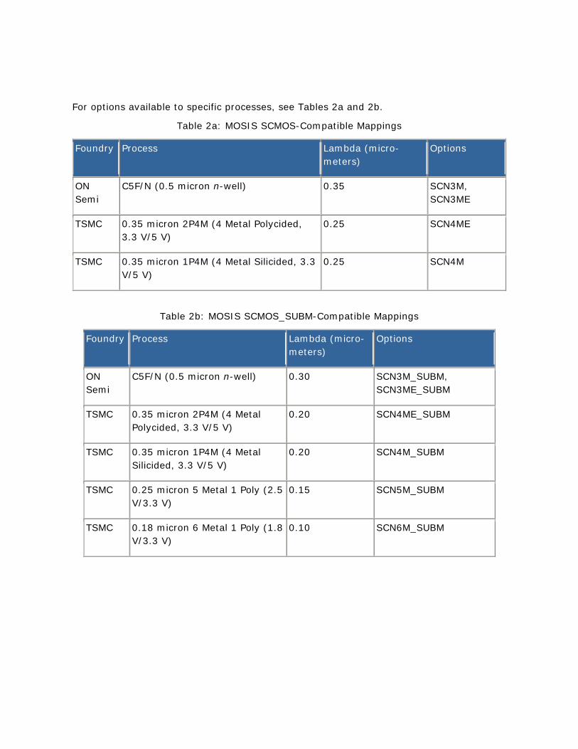
For options available to specific processes, see Tables 2a and 2b.
Table 2a: MOSIS SCMOS-Compatible Mappings
Foundry Process Lambda (micro- meters)
Options
ON Semi
C5F/N (0.5 micron n-well) 0.35 SCN3M, SCN3ME
TSMC 0.35 micron 2P4M (4 Metal Polycided, 3.3 V/5 V)
0.25 SCN4ME
TSMC 0.35 micron 1P4M (4 Metal Silicided, 3.3 V/5 V)
0.25 SCN4M
Table 2b: MOSIS SCMOS_SUBM-Compatible Mappings
Foundry Process Lambda (micro- meters)
Options
ON Semi
C5F/N (0.5 micron n-well) 0.30 SCN3M_SUBM, SCN3ME_SUBM
TSMC 0.35 micron 2P4M (4 Metal Polycided, 3.3 V/5 V)
0.20 SCN4ME_SUBM
TSMC 0.35 micron 1P4M (4 Metal Silicided, 3.3 V/5 V)
0.20 SCN4M_SUBM
TSMC 0.25 micron 5 Metal 1 Poly (2.5 V/3.3 V)
0.15 SCN5M_SUBM
TSMC 0.18 micron 6 Metal 1 Poly (1.8 V/3.3 V)
0.10 SCN6M_SUBM

Table 2c: MOSIS SCMOS_DEEP-Compatible Mappings
Foundry Process Lambda (micro- meters)
Options
TSMC 0.25 micron 5 Metal 1 Poly (2.5 V/3.3 V)
0.12 SCN5M_DEEP
TSMC 0.18 micron 6 Metal 1 Poly (1.8 V/3.3 V)
0.09 SCN6M_DEEP
2.3. SCMOS-Compatible Processes
MOSIS currently offers the fabrication processes shown above in Tables 2a, 2b, and 2c. For each process the list of appropriate SCMOS technology-codes is shown.
2.4. SCMOS_SUBM and SCMOS_DEEP Rules
The SCMOS layout rules were historically developed for 1.0 to 3.0 micron processes. To take full advantage of sub-micron processes, the SCMOS rules were revised to create SCMOS_SUBM. By increasing the lambda size for some rules (those that didn't shrink as fast in practice as did the overall scheme of things), the sub-micron rules allow for use of a smaller value of lambda, and better fit to these small feature size processes. The SCMOS_SUBM rules were revised again at the 0.25 micron regime to better fit the typical deep submicron processes, creating the SCMOS_DEEP variant. Table 3a lists the differences between SCMOS and SCMOS sub-micron. Table 3b lists the differences between SCMOS sub-micron and SCMOS deep.
Table 3a: SCMOS and SCMOS Sub-micron Differences Differences
Rule
Description
SCMOS
SCMOS sub-micron
1.1, 17.1 Well width 10 12
1.2, 17.2 Well space (different potential)
9 18
2.3 Well overlap 5 6

(space) to transistor
3.2 Poly space 2 3
5.3, 6.3 Contact space 2 3
5.5b Contact to Poly space to Poly
4 5
7.2 Metal1 space 2 3
7.4 Minimum space (when metal line is wider than 10 lambda)
4 6
8.5 Via on flat 2 Unrestricted
11.1 Poly2 width 3 7
11.3 Poly2 overlap 2 5
11.5 Space to Poly2 contact 3 6
13.2 Poly2 contact space 2 3
15.1 Metal3 width (3 metal process only)
6 5
15.2 Metal3 space (3 metal process only)
4 3
15.4 Minimum space (when metal line is wider than 10 lambda) (3 metal process only)
8 6
17.3 Minimum spacing to external Active 5 6
17.4 Minimum overlap of Active 5 6
Table 3b: SCMOS Sub-micron and SCMOS Deep Differences
Rule Description SCMOS sub-micron
SCMOS DEEP
3.2 Poly space over field
3 3

3.2.a Poly space over Active
4
3.3 Minimum gate extension of Active
2 2.5
3.4 Active extension beyond Poly
3 4
4.3 Select overlap of Contact
1 1.5
4.4 Select width and space (p+ to p+ or n+ to n+)
2 4
5.3, 6.3 Contact spacing 3 4
8.1 Via width 2 3
9.2 Metal2 space 3 4
9.4 Minimum space (when metal line is wider than 10 lambda)
6 8
14.1 Via2 width 2 3
15.2 Metal3 space 3 4
15.4 Minimum space (when metal line is wider than 10 lambda) (for 4+ metal processes)
6 8
21.1 Via3 width 2 3
22.2 Metal4 space (for 5+ metal processes)
3 4
22.4 Minimum space (when metal line is wider than 10 lambda)
6 8
25.1 Exact size 2 x 2 3 x 3
26.2 Metal5 space 3 4
26.3 Minimum overlap of Via4 1 2

(for 5 metal process only)
26.4 Via4 overlap 6 8
29.1 Exact size 3 x 3 4 x 4
30.3 Minimum overlap of Via5 1 2
3. CIF and GDS Layer Specification
A user design submitted to MOSIS using the SCMOS rules can be in either Calma GDSII format [2] or Caltech Intermediate Form (CIF version 2.0) [1]. The two are completely interchangable. Note that all submitted CIF and GDS files have already been scaled before submission, and are always in absolute metric units -- never in lambda units. GDSII is a binary format, while CIF is a plain ASCII text. For detailed syntax and semantic specifications of GDS and CIF, refer to [2] and [1] respectively. In GDS format, a design layer is specified as a number between 0 and 255. MOSIS SCMOS now reserves layer numbers 21 through 62, inclusive, for drawn layout. Layers 0 through 20 plus layers 63 and above can be used by designers for their own purposes and will be ignored by MOSIS. Users should be aware that there is only one contact mask layer, although several separate layers were defined and are retained for backward compatibility. A complete list of SCMOS layers is shown in Table 4, along with a list by technology code in Table 5.
Table 4: SCMOS Layer Map
Layer GDS CIF CIF Synonym
Rule Section
Notes
N_WELL 42 CWN 1
P_WELL 41 CWP 1 SCPxx
CAP_WELL 59 CWC 17, 18 SCN3MLC
ACTIVE 43 CAA 2
THICK_ ACTIVE
60 CTA 24 SCN4M (TSMC only), SCN4ME, SCN5M, SCN6M

PBASE 58 CBA 16 SCNA
POLY_CAP1 28 CPC 23 SCNPC
POLY 46 CPG 3
SILICIDE_ BLOCK
29 CSB 20 SCN3M, SCN4M (TSMC only), SCN5M, SCN6M
N_PLUS_ SELECT
45 CSN 4
P_PLUS_ SELECT
44 CSP 4
POLY2 56 CEL 11, 12, 13
SCNE, SCNA, SCN3ME, SCN4ME
HI_RES_ IMPLANT
34 CHR 27 SCN3ME
CONTACT 25 CCC CCG 5, 6, 13
POLY_ CONTACT
47 CCP 5 Can be replaced by CONTACT
ACTIVE_ CONTACT
48 CCA 6 Can be replaced by CONTACT
POLY2_ CONTACT
55 CCE 13 SCNE, SCNA, SCN3ME, SCN4ME Can be replaced by CONTACT.
METAL1 49 CM1 CMF 7
VIA 50 CV1 CVA 8
METAL2 51 CM2 CMS 9
VIA2 61 CV2 CVS 14 SCN3M, SCN3ME, SCN3MLC, SCN4M, SCN4ME, SCN5M, SCN6M
METAL3 62 CM3 CMT 15 SCN3M, SCN3ME, SCN3MLC, SCN4M, SCN4ME, SCN5M, SCN6M

VIA3 30 CV3 CVT 21 SCN4M, SCN4ME, SCN5M, SCN6M
METAL4 31 CM4 CMQ 22 SCN4M, SCN4ME, SCN5M, SCN6M
CAP_TOP_ METAL
35 CTM 28 SCN5M. SCN6M
VIA4 32 CV4 CVQ 25 SCN5M, SCN6M
METAL5 33 CM5 CMP 26 SCN5M, SCN6M
VIA5 36 CV5 29 SCN6M
METAL6 37 CM6 30 SCN6M
DEEP_ N_WELL
38 CDNW 31 SCN5M, SCN6M
GLASS 52 COG 10
PADS 26 XP Optional non-fab layer used solely to highlight the bonding pads.
Comments -- CX Comments
Table 5: Technology-code Map
Technology code with link to layer map
Layers
SCNE N_well, Active, N_select, P_select, Poly, Poly2, Contact, Metal1, Via, Metal2, Glass
SCNA N_well, Active, N_select, P_select, Poly, Poly2, Contact, Pbase, Metal1, Via, Metal2, Glass
SCNPC N_well, Active, N_select, P_select, Poly_cap, Poly, Contact, Metal1, Via, Metal2, Glass
SCN3M N_well, Active, N_select, P_select, Poly, Hi_Res_Implant, Contact,

Metal1, Via, Metal2, Via2, Metal3, Glass
SCN3ME N_well, Active, N_select, P_select, Poly, Poly2, Hi_Res_Implant, Contact, Metal1, Via, Metal2, Via2, Metal3, Glass
SCN3MLC N_well, Cap_well, Active, N_select, P_select, Poly, Silicide block, Contact, Metal1, Via, Metal2, Via2, Metal3, Glass
SCN4M N_well, Active, Thick_Active (TSMC only), N_select, P_select, Poly, Contact, Metal1, Via, Metal2, Via2, Metal3, Via3, Metal4, Glass
SCN4ME N_well, Active, Thick_Active, N_select, P_select, Poly, Poly2, Contact, Metal1, Via, Metal2, Via2, Metal3, Via3, Metal4, Glass
SCN5M N_well, Active, Thick_Active, N_select, P_select, Poly, Silicide block, Contact, Metal1, Via, Metal2, Via2, Metal3, Via3, Metal4, Cap_Top_Metal, Via4, Metal5, Deep_N_Well, Glass
SCN6M N_well, Active, Thick_Active, N_select, P_select, Poly, Silicide block, Contact, Metal1, Via, Metal2, Via2, Metal3, Via3, Metal4, Via4, Metal5, Cap_Top_Metal, Via5, Metal6, Deep_N_Well, Glass
4. Minimum Density Rule
Many fine-featured processes utilize CMP (Chemical-Mechanical Polishing) to achieve planarity. Currently, for MOSIS, the ON Semi 0.50 micron and all the 0.35 micron (and smaller) processes are in this category. Effective CMP requires that the variations in feature density on layer be restricted. See the following for more details.
5. Process-Induced Damage Rules (otherwise known as "Antenna Rules"): General Requirements
The "Antenna Rules" deal with process induced gate oxide damage caused when exposed polysilicon and metal structures, connected to a thin oxide transistor, collect charge from the processing environment (e.g., reactive ion etch) and develop potentials sufficiently large to cause Fowler Nordheim current to flow through the thin oxide. Given the known process charge fluence, a figure of exposed conductor area to transistor gate area ratio is determined which guarantees Time Dependent Dielectric Breakdown (TDDB) reliability requirements for the fabricator. Failure to consider antenna rules in a design may lead to either reduced performance in transistors exposed to process induced damage, or may
lead to total failure if the antenna rules are seriously violated.
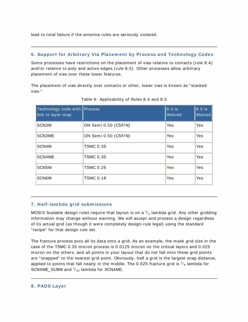
6. Support for Arbitrary Via Placement by Process and Technology Codes
Some processes have restrictions on the placement of vias relative to contacts (rule 8.4) and/or relative to poly and active edges (rule 8.5). Other processes allow arbitrary placement of vias over these lower features. The placement of vias directly over contacts or other, lower vias is known as "stacked vias."
Table 6: Applicability of Rules 8.4 and 8.5
Technology code with link to layer map
Process 8.4 is Waived
8.5 is Waived
SCN3M ON Semi 0.50 (C5F/N) Yes Yes
SCN3ME ON Semi 0.50 (C5F/N) Yes Yes
SCN4M TSMC 0.35 Yes Yes
SCN4ME TSMC 0.35 Yes Yes
SCN5M TSMC 0.25 Yes Yes
SCN6M TSMC 0.18 Yes Yes
7. Half-lambda grid submissions
MOSIS Scalable design rules require that layout is on a 1⁄2 lambda grid. Any other gridding information may change without warning. We will accept and process a design regardless of its actual grid (as though it were completely design-rule legal) using the standard "recipe" for that design rule set. The fracture process puts all its data onto a grid. As an example, the mask grid size in the case of the TSMC 0.35 micron process is 0.0125 micron on the critical layers and 0.025 micron on the others, and all points in your layout that do not fall onto these grid points are "snapped" to the nearest grid point. Obviously, half a grid is the largest snap distance, applied to points that fall neatly in the middle. The 0.025 fracture grid is 1⁄8 lambda for SCN4ME_SUBM and 1⁄10 lambda for SCN4ME.
8. PADS Layer

MOSIS has defined an optional PADS layer to help users tell MOSIS which glass openings are to be bonded and which are not. This optional layer lets you call out only those glass cuts that you want MOSIS to use in generating an automated bonding for your project. When used, PADS should match the glass cuts (or the larger metal pads underneath) for just the selected glass cuts. Geometry on the PADS layer has absolutely no influence on chip fabrication. When the PADS layer is not present, MOSIS will analyze the glass cuts to determine which appear to be bonding pads and which do not. For the vast majority of layouts, the PADS layer is unnecessary.
References
[1] C. Mead and L. Conway, Introduction to VLSI Systems, Addison-Wesley, 1980 [2] Cadence Design Systems, Inc./Calma. GDSII Stream Format Manual, Feb. 1987, Release 6.0, Documentation No. B97E060 [3] N. H. E. Weste and K. Eshraghian, Principles of CMOS VLSI Design: A System Perspective, Addison-Wesley, 2nd edition, 1993

SCMOS Layout Rules - DEEP_N_WELL for SCMOS_DEEP (and SUBM)
The DEEP_N_WELL layer provides access to the DNW layer in the TSMC 0.18 and 0.25 processes. This provides a layering sometimes called "triple-well" in which an n-well sits in the p-substrate, and then a p-well sits fully inside of the n-well; it is then possible to construct NMOS devices inside of that isolated p-well. The isolated p-well is surrounded by a fence of standard N_WELL (around its periphery), and by DEEP_N_WELL underneath. The N_WELL fence makes direct electrical contact with the DEEP_N_WELL plate beneath it. DEEP_N_WELL is available in technology codes SCN5M_SUBM, SCN5M_DEEP, SCN6M_SUBM and SCN6M_DEEP but only where these are to be fabricated on TSMC foundry runs. To gain a better understanding of this layer, the TSMC vendor-rule design rule documentation should be studied.
Rule Description Lambda
SCMOS SUBM DEEP
31.1 Minimum Width, Deep_N_Well n/a 30 34
31.2 Minimum Spacing, Deep_N_Well to Deep_N_Well n/a 50 56
31.3 Minimum extension, N_Well beyond Deep_N_Well edge n/a 15 17
31.4 Minimum overlap, N_Well over Deep_N_Well edge n/a 20 23
31.5 Minimum spacing, Deep_N_Well to unrelated N_Well n/a 35 39
31.6 Minimum spacing, N+Active in isolated P-well, to N_Well n/a 5 6
31.7 Minimum spacing, external N+Active to Deep_N_Well n/a 30 34
31.8 Minimum spacing, P+Active in N_Well to its Deep_N_Well
n/a 10 13


SCMOS Layout Rules - Well
Rule Description Lambda
SCMOS SUBM DEEP
1.1 Minimum width 10 12 12
1.2 Minimum spacing between wells at different potential 9 18 18
1.3 Minimum spacing between wells at same potential 6 6 6
1.4 Minimum spacing between wells of different type (if both are drawn)
0 0 0

SCMOS Layout Rules - Capacitor Well
The capacitor well described in this and the next rule only apply to SCN3MLC and SCN3MLC_SUBM technology codes manufactured on an Agilent/HP AMOS14TB run.
Rule Description Lambda
SCMOS SUBM DEEP
17.1 Minimum width 10 12 n/a
17.2 Minimum spacing 9 18 n/a
17.3 Minimum spacing to external active 5 6 n/a
17.4 Minimum overlap of active 5 6 n/a

SCMOS Layout Rules - Linear Capacitor (Linear Capacitor Option)
These rules illustrate the construction of a linear capacitor in a capacitor well. The capacitor itself is the region of overlapped poly and active. The active area is electrically connected to the cap well
Rule Description Lambda
SCMOS SUBM DEEP
18.1 Minimum width 3 3 n/a
18.2 Minimum poly extension of active 2 2 n/a
18.3 Minimum active overlap of poly 3 3 n/a
18.4 Minimum poly contact to active 2 2 n/a
18.5 Minimum active contact to poly 6 6 n/a

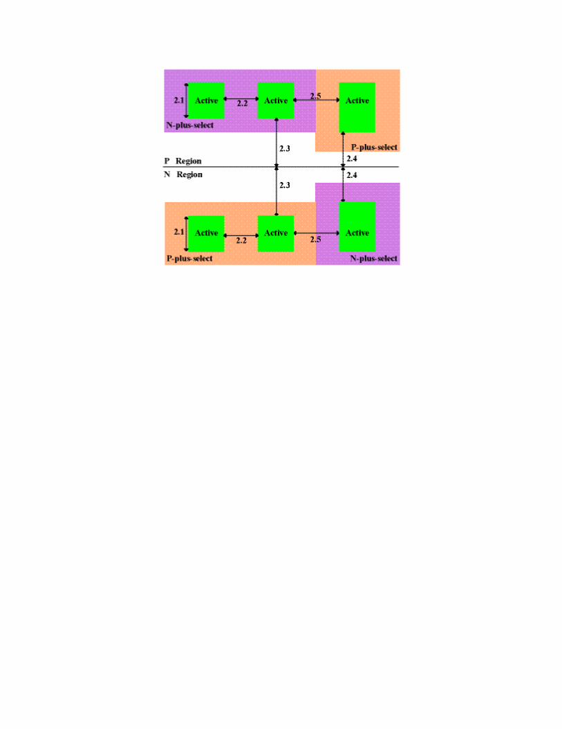
SCMOS Layout Rules - Active
Rule Description Lambda
SCMOS SUBM DEEP
2.1 Minimum width 3 * 3 * 3
2.2 Minimum spacing 3 3 3
2.3 Source/drain active to well edge 5 6 6
2.4 Substrate/well contact active to well edge 3 3 3
2.5 Minimum spacing between non-abutting active of different implant. Abutting active ("split-active") is illustrated under Select Layout Rules.
4 4 4
* Note: For analog and critical digital designs, MOSIS recommends the following minimum MOS channel widths (active under poly) for ON Semiconductor designs. Narrower devices, down to design rule minimum, will be functional, but their electrical characteristics will not scale, and their performance is not predictable from MOSIS SPICE parameters.
Process Design Technology Design Lambda (micrometers)
Minimum Width (lambda)
AMI_C5F/N SCN3M, SCN3ME 0.35 9
AMI_C5F/N SCN3M_SUBM, SCN3ME_SUBM
0.30 10

SCMOS Layout Rules - Thick Active
THICK_ACTIVE is a layer used for those processes offering two different thicknesses of gate oxide (typically for the layout of transistors that operate at two different voltage levels). The ACTIVE layer is used to delineate all the active areas, regardless of gate oxide thickness. THICK_ACTIVE is used to mark those ACTIVE areas that will have the thicker gate oxide; ACTIVE areas outside THICK_ACTIVE will have the thinner gate oxide. THICK_ACTIVE by itself (not covering any ACTIVE polygon) is meaningless.
Rule Description Lambda
SCMOS SUBM DEEP
24.1 Minimum width 4 4 4
24.2 Minimum spacing 4 4 4
24.3 Minimum ACTIVE overlap 4 4 4
24.4 Minimum space to external ACTIVE 4 4 4
24.5 Minimum poly width in a THICK_ACTIVE gate 3 3 3
24.6 Every ACTIVE region is either entirely inside THICK_ACTIVE or entirely outside THICK_ACTIVE
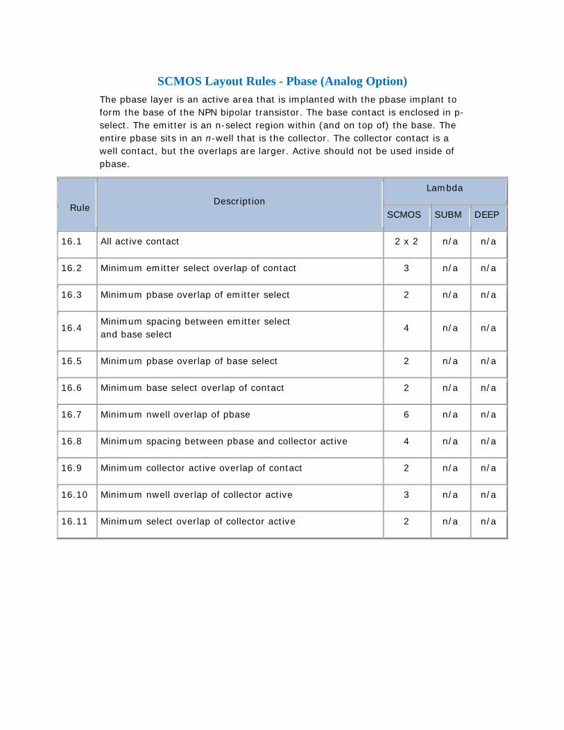
SCMOS Layout Rules - Pbase (Analog Option) The pbase layer is an active area that is implanted with the pbase implant to form the base of the NPN bipolar transistor. The base contact is enclosed in p-select. The emitter is an n-select region within (and on top of) the base. The entire pbase sits in an n-well that is the collector. The collector contact is a well contact, but the overlaps are larger. Active should not be used inside of pbase.
Rule
Description Lambda
SCMOS SUBM DEEP
16.1 All active contact 2 x 2 n/a n/a
16.2 Minimum emitter select overlap of contact 3 n/a n/a
16.3 Minimum pbase overlap of emitter select 2 n/a n/a
16.4 Minimum spacing between emitter select and base select
4 n/a n/a
16.5 Minimum pbase overlap of base select 2 n/a n/a
16.6 Minimum base select overlap of contact 2 n/a n/a
16.7 Minimum nwell overlap of pbase 6 n/a n/a
16.8 Minimum spacing between pbase and collector active 4 n/a n/a
16.9 Minimum collector active overlap of contact 2 n/a n/a
16.10 Minimum nwell overlap of collector active 3 n/a n/a
16.11 Minimum select overlap of collector active 2 n/a n/a


SCMOS Layout Rules - SCNPC with POLY_CAP
The two plates of an SCNPC capacitor are POLY and POLY_CAP1. The POLY_CAP1 must surround the POLY everywhere; the area of the capacitor is the area of the POLY. POLY is physically on top of POLY_CAP1, so that contact to the POLY_CAP1 must be made in the region where it extends beyond the POLY. The capacitor may be in the well or the substrate, but may not straddle a well boundary. The only metal that may cross over a capacitor is the connecting METAL1 wires.
Rule Description Lambda
SCMOS SUBM DEEP
23.1 Minimum POLY_CAP1 width. This is lithographic; the minimum to build a real capacitor is greater than 12 lambda
8 n/a n/a
23.2 Minimum spacing, POLY_CAP1 to POLY_CAP1 (neighboring capacitor)
4 n/a n/a
23.3 Minimum spacing, POLY_CAP1 to ACTIVE (all capacitors must be over field)
8 n/a n/a
23.4 Minimum overlap, POLY_CAP1 over POLY 3 n/a n/a
23.5 Minimum overlap, POLY_CAP1 over CONTACT 2 n/a n/a
23.6 Minimum overlap, POLY over CONTACT (in a capacitor only; still 1 lambda elsewhere)
2 n/a n/a
23.7 Minimum spacing, POLY to CONTACT-to-POLY_CAP1 2 n/a n/a
23.8 Minimum spacing, unrelated METAL1 to POLY_CAP1 4 n/a n/a
23.9 Minimum spacing, METAL2 to POLY_CAP1 2 n/a n/a


SCMOS Layout Rules - Poly
Rule Description Lambda
SCMOS SUBM DEEP
3.1 Minimum width 2 2 2
3.2 Minimum spacing over field 2 3 3
3.2.a Minimum spacing over active 2 3 4
3.3 Minimum gate extension of active 2 2 2.5
3.4 Minimum active extension of poly 3 3 4
3.5 Minimum field poly to active 1 1 1

SCMOS Layout Rules - Silicide Block
Rule Description Lambda
SCMOS SUBM DEEP
20.1 Minimum SB width 4 4 4
20.2 Minimum SB spacing 4 4 4
20.3 Minimum spacing, SB to contact (no contacts allowed inside SB)
2 2 2
20.4 Minimum spacing, SB to external active 2 2 2
20.5 Minimum spacing, SB to external poly 2 2 2
20.6 Resistor is poly inside SB; poly ends stick out for contacts the entire resistor must be outside well and over field
20.7 Minimum poly width in resistor 5 5 5
20.8 Minimum spacing of poly resistors (in a single SB region)
7 7 7
20.9 Minimum SB overlap of poly or active 2 2 2
20.10 Minimum poly or active overlap of SB 3 3 3
20.11 Minimum spacing, SB to poly (in a single active region)
3 5 5
NOTE: Some processes do not support both silicide block over active and silicide block over poly. Refer to the individual process description pages.


SCMOS Layout Rules - Select
Rule Description Lambda
SCMOS SUBM DEEP
4.1 Minimum select spacing to channel of transistor to ensure adequate source/drain width
3 3 3
4.2 Minimum select overlap of active 2 2 2
4.3 Minimum select overlap of contact 1 1 1.5
4.4 Minimum select width and spacing (Note: P-select and N-select may be coincident, but must not overlap) (not illustrated)
2 2 4
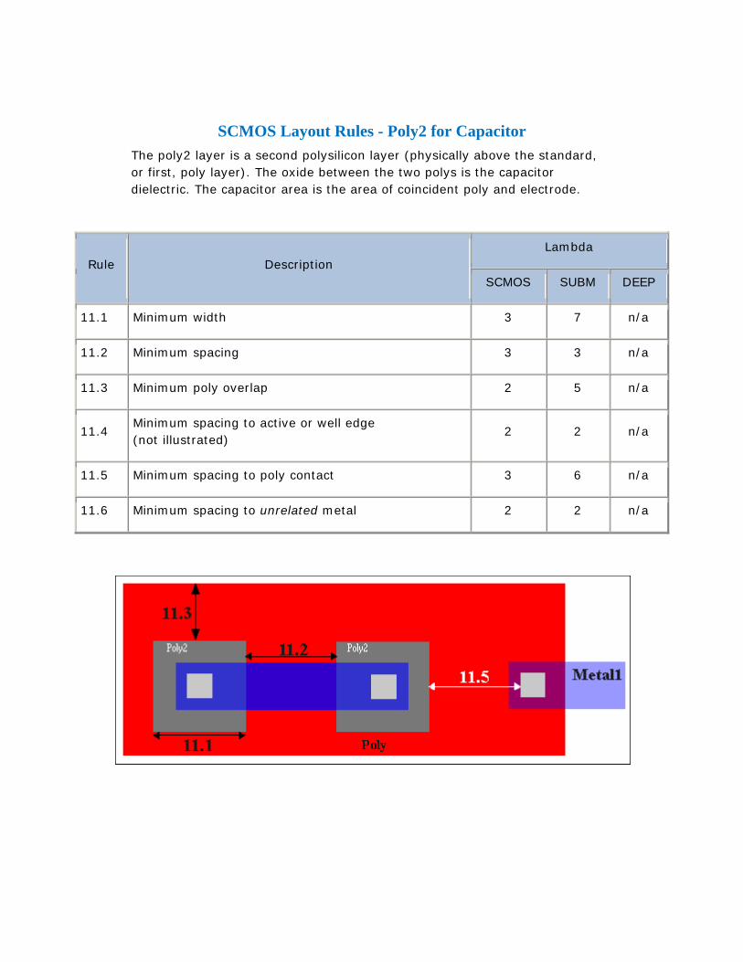
SCMOS Layout Rules - Poly2 for Capacitor
The poly2 layer is a second polysilicon layer (physically above the standard, or first, poly layer). The oxide between the two polys is the capacitor dielectric. The capacitor area is the area of coincident poly and electrode.
Rule Description Lambda
SCMOS SUBM DEEP
11.1 Minimum width 3 7 n/a
11.2 Minimum spacing 3 3 n/a
11.3 Minimum poly overlap 2 5 n/a
11.4 Minimum spacing to active or well edge (not illustrated)
2 2 n/a
11.5 Minimum spacing to poly contact 3 6 n/a
11.6 Minimum spacing to unrelated metal 2 2 n/a

SCMOS Layout Rules - Poly2 for Transistor Same poly2 layer as for caps
Rule Description Lambda
SCMOS SUBM DEEP
12.1 Minimum width 2 2 n/a
12.2 Minimum spacing 3 3 n/a
12.3 Minimum electrode gate overlap of active 2 2 n/a
12.4 Minimum spacing to active 1 1 n/a
12.5 Minimum spacing or overlap of poly 2 2 n/a
12.6 Minimum spacing to poly or active contact 3 3 n/a

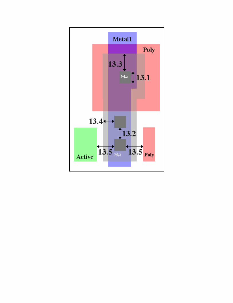
SCMOS Layout Rules - Poly2 Contact
The poly2 is contacted through the standard contact layer, similar to the first poly. The overlap numbers are larger, however. Contacts must be drawn orthogonal to the grid of the layout. Non-Manhattan contacts are not allowed.
Rule Description Lambda
SCMOS SUBM DEEP
13.1 Exact contact size 2 x 2 2 x 2 n/a
13.2 Minimum contact spacing 2 3 n/a
13.3 Minimum electrode overlap (on capacitor) 3 3 n/a
13.4 Minimum electrode overlap (not on capacitor) 2 2 n/a
13.5 Minimum spacing to poly or active 3 3 n/a

SCMOS Layout Rules - High Res
Rule Description Lambda
SCMOS SUBM DEEP
27.1 Minimum HR width 4 4 n/a
27.2 Minimum HR spacing 4 4 n/a
27.3 Minimum spacing, HR to contact (no contacts allowed inside HR)
2 2 n/a
27.4 Minimum spacing, HR to external active 2 2 n/a
27.5 Minimum spacing, HR to external poly2 2 2 n/a
27.6 Resistor is poly2 inside HR; poly2 ends stick out for contacts, the entire resistor must be outside well and over field
27.7 Minimum poly2 width in resistor 5 5 n/a
27.8 Minimum spacing of poly2 resistors (in a single HR region)
7 7 n/a
27.9 Minimum HR overlap of poly2 2 2 n/a

SCMOS Layout Rules - Contact to Poly
On 0.50 micron process (and all finer feature size processes), it is required that all features on the insulator layers (CONTACT, VIA, VIA2) must be of the single standard size; there are no exceptions for pads (or logos, or anything else); large openings must be replaced by an array of standard sized openings. Contacts must be drawn orthogonal to the grid of the layout. Non-Manhattan contacts are not allowed. If your design cannot tolerate 1.5 lambda contact overlap in 5.2, use the alternative rules which reduce the overlap but increase the spacing to surrounding features. Rules 5.1, 5.3, and 5.4, still apply and are unchanged.
Simple Contact to Poly
Alternative Contact to Poly
Rule Description Lambda
SCMOS SUBM DEEP
5.1 Exact contact size
2x2 2x2 2x2
5.2 Minimum poly overlap
1.5 1.5 1.5
5.3 Minimum contact spacing
2 3 4
5.4 Minimum spacing to gate of transistor
2 2 2
Rule Description Lambda
SCMOS SUBM DEEP
5.2.b Minimum poly overlap
1 1 1
5.5.b Minimum spacing to other poly
4 5 5
5.6.b
Minimum spacing to active (one contact)
2 2 2
5.7.b
Minimum spacing to active (many contacts)
3 3 3

Simple Poly to Contact Alternative Contact to Poly

SCMOS Layout Rules - Contact to Active
If your design cannot handle the 1.5 lambda contact overlap in 6.2, use the alternative rules which reduce the overlap but increase the spacing to surrounding features. Rules 6.1, 6.3, and 6.4, still apply and are unchanged. Contacts must be drawn orthogonal to the grid of the layout. Non-Manhattan contacts are not allowed.
Simple Contact to Active
Alternative Contact to Active
Rule Description Lambda
SCMOS SUBM DEEP
6.1 Exact contact size
2x2 2x2 2x2
6.2 Minimum active overlap
1.5 1.5 1.5
6.3 Minimum contact spacing
2 3 4
6.4 Minimum spacing to gate of transistor
2 2 2
Rule Description Lambda
SCMOS SUBM DEEP
6.2.b Minimum active overlap
1 1 1
6.5.b Minimum spacing to diffusion active
5 5 5
6.6.b
Minimum spacing to field poly (one contact)
2 2 2
6.7.b
Minimum spacing to field poly (many contacts)
3 3 3
6.8.b Minimum spacing to poly contact
4 4 4
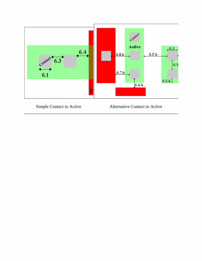
Simple Contact to Active Alternative Contact to Active
SCMOS Layout Rules - Metal1
Rule Description Lambda
SCMOS SUBM DEEP
7.1 Minimum width 3 3 3
7.2 Minimum spacing 2 3 3
7.3 Minimum overlap of any contact 1 1 1
7.4 Minimum spacing when either metal line is wider than 10 lambda
4 6 6

SCMOS Layout Rules - Via
Vias must be drawn orthogonal to the grid of the layout. Non-Manhattan vias are not allowed.
Rule Description
Lambda
2 Metal Process 3+ Metal Process
SCMOS SUBM DEEP SCMOS SUBM DEEP
8.1 Exact size 2 x 2 n/a n/a 2 x 2 2 x 2 3 x 3
8.2 Minimum via1 spacing 3 n/a n/a 3 3 3
8.3 Minimum overlap by metal1 1 n/a n/a 1 1 1
8.4 Minimum spacing to contact for technology codes mapped to processes that do not allow stacked vias (SCNA, SCNE, SCN3M, SCN3MLC)
2 n/a n/a 2 2 n/a
8.5
Minimum spacing to poly or active edge for technology codes mapped to processes that do not allow stacked vias (NOTE: list is not same as for 8.4)
2 n/a n/a 2 2 n/a

SCMOS Layout Rules - Metal2
Rule Description
Lambda
2 Metal Process 3+ Metal Process
SCMOS SUBM DEEP SCMOS SUBM DEEP
9.1 Minimum width 3 n/a n/a 3 3 3
9.2 Minimum spacing 3 n/a n/a 3 3 4
9.3 Minimum overlap of via1 1 n/a n/a 1 1 1
9.4 Minimum spacing when either metal line is wider than 10 lambda
6 n/a n/a 6 6 8

SCMOS Layout Rules - Via2
Vias must be drawn orthogonal to the grid of the layout. Non-Manhattan vias are not allowed.
Rule Description
Lambda
3 Metal Process 4+ Metal Process
SCMOS SUBM DEEP SCMOS SUBM DEEP
14.1 Exact size 2x2 2x2 n/a 2x2 2x2 3x3
14.2 Minimum spacing 3 3 n/a 3 3 3
14.3 Minimum overlap by metal2 1 1 n/a 1 1 1
14.4 Via2 may be placed over via1
14.5 Via2 may be placed over contact
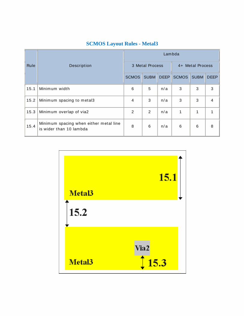
SCMOS Layout Rules - Metal3
Rule Description
Lambda
3 Metal Process 4+ Metal Process
SCMOS SUBM DEEP SCMOS SUBM DEEP
15.1 Minimum width 6 5 n/a 3 3 3
15.2 Minimum spacing to metal3 4 3 n/a 3 3 4
15.3 Minimum overlap of via2 2 2 n/a 1 1 1
15.4 Minimum spacing when either metal line is wider than 10 lambda
8 6 n/a 6 6 8

SCMOS Layout Rules - Via3
Vias must be drawn orthogonal to the grid of the layout. Non-Manhattan vias are not allowed.
Rule Description
Lambda
4 metal Process 5+ Metal Process
SCMOS SUBM DEEP SCMOS SUBM DEEP
21.1 Exact size 2x2 2x2 n/a n/a 2x2 3x3
21.2 Minimum spacing 3 3 * n/a n/a 3 3
21.3 Minimum overlap by Metal3 1 1 n/a n/a 1 1
* Exception: Use lambda=4 for rule 21.2 only when using SCN4M_SUBM for Agilent/HP GMOS10QA 0.35 micron process

SCMOS Layout Rules - Metal4
Rule Description
Lambda
4 Metal Process 5+ Metal Process
SCMOS SUBM DEEP SCMOS SUBM DEEP
22.1 METAL4 width 6 6 n/a n/a 3 3
22.2 METAL4 space 6 6 n/a n/a 3 4
22.3 METAL4 overlap of VIA3 2 2 n/a n/a 1 1
22.4 Minimum spacing when either metal line is wider than 10 lambda
12 12 n/a n/a 6 8

SCMOS Layout Rules - CAP_TOP_METAL for SCMOS_DEEP (and SUBM)
The CAP_TOP_METAL layer is used exclusively for the construction of metal-to-metal capacitors. The bottom plate of the capacitor is one of the regular metal layers, as specified below. CAP_TOP_METAL is the upper plate of the capacitor; it is sandwiched physically between the bottom plate metal and the next metal layer above, with a thin dielectric between the bottom plate and the upper (CAP_TOP_METAL) plate. The CAP_TOP_METAL can only be contacted from the metal above; the bottom plate metal can be contacted from below or above (subject, in either case, to rule 28.5), and/or by bottom metal extending outside of the capacitor region (rule 28.7). Use of all (legal) upward vias within that region should be maximized. CAP_TOP_METAL must always be contained entirely within the bottom plate metal.
Process Bottom Plate Top Plate Top Plate Contact
TSMC_025 METAL4 CAP_TOP_METAL VIA4 and METAL5
TSMC_018 METAL5 CAP_TOP_METAL VIA5 and METAL6
Rule Description Lambda
SCMOS SUBM DEEP
28.1 Minimum Width, Capacitor n/a 40 45
28.2 Minimum Spacing (2 capacitors sharing a single bottom plate)
n/a 12 14
28.3 Minimum bottom metal overlap (including dummy shapes)
n/a 4 5
28.4 Minimum overlap of via n/a 3 3
28.5 Minimum spacing to bottom metal via n/a 4 5
28.6 Minimum bottom metal overlap of its via n/a 2 2

28.7 Rule applicability region extends beyond bottom plate
n/a 25 25
28.8 Minimum width, dummy shapes (having no vias) n/a 4 5
28.9 Minimum bottom plate to other bottom plate metal
n/a 8 9
28.10 Minimum via separation, on CAP_TOP_METAL n/a 20 23
28.11 Minimum (upward) via separation on bottom metal
n/a 40 45
28.12 Maximum CAP_TOP_METAL width and length n/a 30 um
28.13 Maximum bottom metal plate width and length n/a 35 um
28.14 No vias from bottom plate downward, directly under top plate CAP_TOP_METAL; dummy metal shapes under capacitor region, discouraged.
28.15 No active or passive circuitry under capacitor region


SCMOS Layout Rules - Via4 (SUBM and DEEP)
Vias must be drawn orthogonal to the grid of the layout. Non-Manhattan vias are not allowed.
Rule Description
Lambda
5 Metal Process 6+ Metal Process
SCMOS SUBM DEEP SCMOS SUBM DEEP
25.1 Exact size n/a 2x2 3x3 n/a 2x2 3x3
25.2 Minimum spacing n/a 3 3 n/a 3 3
25.3 Minimum overlap by Metal4 n/a 1 1 n/a 1 1

SCMOS Layout Rules - Metal5 (SUBM and DEEP)
Any designer using the SCMOS rules who wants the TSMC Thick_Top_Metal must draw the top metal to comply with the TSMC rules for that layer.
Rule Description
Lambda
5 Metal Process 6+ Metal Process
SCMOS SUBM DEEP SCMOS SUBM DEEP
26.1 Minimum width n/a 4 4 n/a 3 3
26.2 Minimum spacing to Metal5 n/a 4 4 n/a 3 4
26.3 Minimum overlap of Via4 n/a 1 2 n/a 1 1
26.4 Minimum spacing when either metal line is wider than 10 lambda
n/a 8 8 n/a 6 8

SCMOS Layout Rules - Via5 (SUBM and DEEP)
Vias must be drawn orthogonal to the grid of the layout. Non-Manhattan vias are not allowed.
Rule Description
Lambda
6 Metal Process
SCMOS SUBM DEEP
29.1 Exact size n/a 3 x 3 4 x 4
29.2 Minimum spacing n/a 4 4
29.3 Minimum overlap by Metal5 n/a 1 1

SCMOS Layout Rules - Metal6 (SUBM and DEEP)
Any designer using the SCMOS rules who wants the TSMC Thick_Top_Metal must draw the top metal to comply with the TSMC rules for that layer.
Rule Description
Lambda
6 Metal Process
SCMOS SUBM DEEP
30.1 Minimum width n/a 5 5
30.2 Minimum spacing to Metal6 n/a 5 5
30.3 Minimum overlap of Via5 n/a 1 2
30.4 Minimum spacing when either metal line is wider than 10 lambda
n/a 10 10

SCMOS Layout Rules - Overglass
Note that rules in this section are in units of microns, not lambda. They are not "true" design rules, but they do make good practice rules. Unfortunately, there are no really good generic pad design rules since pads are process-specific.
Rule Description Microns
(not lambda)
10.1 Minimum bonding passivation opening 60
10.2 Minimum probe passivation opening 20
10.3 Pad metal overlap of passivation 6
10.4 Minimum pad spacing to unrelated metal 30
10.5 Minimum pad spacing to active, poly or poly2 15